WO2009104652A1 - 白色発光装置及びこれを用いた車両用灯具 - Google Patents
白色発光装置及びこれを用いた車両用灯具 Download PDFInfo
- Publication number
- WO2009104652A1 WO2009104652A1 PCT/JP2009/052819 JP2009052819W WO2009104652A1 WO 2009104652 A1 WO2009104652 A1 WO 2009104652A1 JP 2009052819 W JP2009052819 W JP 2009052819W WO 2009104652 A1 WO2009104652 A1 WO 2009104652A1
- Authority
- WO
- WIPO (PCT)
- Prior art keywords
- phosphor
- light emitting
- emitting device
- white light
- range
- Prior art date
- Legal status (The legal status is an assumption and is not a legal conclusion. Google has not performed a legal analysis and makes no representation as to the accuracy of the status listed.)
- Ceased
Links
Images






Classifications
-
- C—CHEMISTRY; METALLURGY
- C09—DYES; PAINTS; POLISHES; NATURAL RESINS; ADHESIVES; COMPOSITIONS NOT OTHERWISE PROVIDED FOR; APPLICATIONS OF MATERIALS NOT OTHERWISE PROVIDED FOR
- C09K—MATERIALS FOR MISCELLANEOUS APPLICATIONS, NOT PROVIDED FOR ELSEWHERE
- C09K11/00—Luminescent materials, e.g. electroluminescent or chemiluminescent
- C09K11/08—Luminescent materials, e.g. electroluminescent or chemiluminescent containing inorganic luminescent materials
- C09K11/0883—Arsenides; Nitrides; Phosphides
-
- C—CHEMISTRY; METALLURGY
- C09—DYES; PAINTS; POLISHES; NATURAL RESINS; ADHESIVES; COMPOSITIONS NOT OTHERWISE PROVIDED FOR; APPLICATIONS OF MATERIALS NOT OTHERWISE PROVIDED FOR
- C09K—MATERIALS FOR MISCELLANEOUS APPLICATIONS, NOT PROVIDED FOR ELSEWHERE
- C09K11/00—Luminescent materials, e.g. electroluminescent or chemiluminescent
- C09K11/08—Luminescent materials, e.g. electroluminescent or chemiluminescent containing inorganic luminescent materials
- C09K11/77—Luminescent materials, e.g. electroluminescent or chemiluminescent containing inorganic luminescent materials containing rare earth metals
- C09K11/7728—Luminescent materials, e.g. electroluminescent or chemiluminescent containing inorganic luminescent materials containing rare earth metals containing europium
- C09K11/77342—Silicates
-
- C—CHEMISTRY; METALLURGY
- C09—DYES; PAINTS; POLISHES; NATURAL RESINS; ADHESIVES; COMPOSITIONS NOT OTHERWISE PROVIDED FOR; APPLICATIONS OF MATERIALS NOT OTHERWISE PROVIDED FOR
- C09K—MATERIALS FOR MISCELLANEOUS APPLICATIONS, NOT PROVIDED FOR ELSEWHERE
- C09K11/00—Luminescent materials, e.g. electroluminescent or chemiluminescent
- C09K11/08—Luminescent materials, e.g. electroluminescent or chemiluminescent containing inorganic luminescent materials
- C09K11/77—Luminescent materials, e.g. electroluminescent or chemiluminescent containing inorganic luminescent materials containing rare earth metals
- C09K11/7728—Luminescent materials, e.g. electroluminescent or chemiluminescent containing inorganic luminescent materials containing rare earth metals containing europium
- C09K11/77347—Silicon Nitrides or Silicon Oxynitrides
-
- H—ELECTRICITY
- H10—SEMICONDUCTOR DEVICES; ELECTRIC SOLID-STATE DEVICES NOT OTHERWISE PROVIDED FOR
- H10H—INORGANIC LIGHT-EMITTING SEMICONDUCTOR DEVICES HAVING POTENTIAL BARRIERS
- H10H20/00—Individual inorganic light-emitting semiconductor devices having potential barriers, e.g. light-emitting diodes [LED]
- H10H20/80—Constructional details
- H10H20/85—Packages
- H10H20/851—Wavelength conversion means
- H10H20/8511—Wavelength conversion means characterised by their material, e.g. binder
- H10H20/8512—Wavelength conversion materials
-
- H—ELECTRICITY
- H10—SEMICONDUCTOR DEVICES; ELECTRIC SOLID-STATE DEVICES NOT OTHERWISE PROVIDED FOR
- H10H—INORGANIC LIGHT-EMITTING SEMICONDUCTOR DEVICES HAVING POTENTIAL BARRIERS
- H10H20/00—Individual inorganic light-emitting semiconductor devices having potential barriers, e.g. light-emitting diodes [LED]
- H10H20/80—Constructional details
- H10H20/85—Packages
- H10H20/851—Wavelength conversion means
- H10H20/8511—Wavelength conversion means characterised by their material, e.g. binder
- H10H20/8512—Wavelength conversion materials
- H10H20/8513—Wavelength conversion materials having two or more wavelength conversion materials
-
- H—ELECTRICITY
- H10—SEMICONDUCTOR DEVICES; ELECTRIC SOLID-STATE DEVICES NOT OTHERWISE PROVIDED FOR
- H10W—GENERIC PACKAGES, INTERCONNECTIONS, CONNECTORS OR OTHER CONSTRUCTIONAL DETAILS OF DEVICES COVERED BY CLASS H10
- H10W72/00—Interconnections or connectors in packages
- H10W72/851—Dispositions of multiple connectors or interconnections
- H10W72/874—On different surfaces
- H10W72/884—Die-attach connectors and bond wires
-
- Y—GENERAL TAGGING OF NEW TECHNOLOGICAL DEVELOPMENTS; GENERAL TAGGING OF CROSS-SECTIONAL TECHNOLOGIES SPANNING OVER SEVERAL SECTIONS OF THE IPC; TECHNICAL SUBJECTS COVERED BY FORMER USPC CROSS-REFERENCE ART COLLECTIONS [XRACs] AND DIGESTS
- Y02—TECHNOLOGIES OR APPLICATIONS FOR MITIGATION OR ADAPTATION AGAINST CLIMATE CHANGE
- Y02B—CLIMATE CHANGE MITIGATION TECHNOLOGIES RELATED TO BUILDINGS, e.g. HOUSING, HOUSE APPLIANCES OR RELATED END-USER APPLICATIONS
- Y02B20/00—Energy efficient lighting technologies, e.g. halogen lamps or gas discharge lamps
Definitions
- the present invention relates to a white light emitting device used for a vehicular lamp and a vehicular lamp using the same. More specifically, white light having high visibility within a chromaticity stipulated range of a white light source used for a vehicular lamp using a semiconductor light emitting element and a phosphor that is efficiently excited and emitted by light from the semiconductor light emitting element.
- the present invention relates to a white light emitting device capable of emitting light with high light emission intensity and high color rendering properties, and a vehicle lamp using the same.
- a white light emitting device with long life and low power consumption a semiconductor light emitting diode (LED) or a laser diode (LD) emitting blue light and a phosphor using these as an excitation light source are combined.
- LED semiconductor light emitting diode
- LD laser diode
- White light-emitting devices configured to obtain white light as a combined spectrum obtained by additive color mixing of light emission obtained from the above are attracting attention, and the use thereof is used as a white light source for vehicle lamps, particularly vehicle headlamps. Is expected.
- the white light source of the vehicular lamp is required to have an emission spectrum within a predetermined chromaticity coordinate (cx, cy) range according to chromaticity regulations.
- JIS: D5500 It is required to be within the area A shown in the chromaticity diagram of 1.
- the region A is represented by the following formula. ⁇ Chromaticity regulation of white light source for vehicle headlamps (JIS: D5500)> Yellow direction cx ⁇ 0.50 Blue direction cx ⁇ 0.31 Green direction cy ⁇ 0.44 and cy ⁇ 0.15 + 0.64cx Purple direction cy ⁇ 0.05 + 0.75 cx and cy ⁇ 0.382
- an InGaN-based semiconductor light emitting element having an emission peak wavelength in a blue wavelength range (420 to 490 nm), 510 2.
- a white light emitting device that realizes white light emission by combining a cerium-activated yttrium aluminum garnet (YAG) yellow phosphor having an emission peak wavelength between ⁇ 600 nm is known. (See Patent Document 2) Japanese Patent Application Publication No. 2004-095480 Japanese Patent No. 3503139
- the chromaticity range that can be reproduced by a white light emitting device combining a semiconductor light emitting element that emits blue light and a yellow phosphor is the chromaticity coordinates of blue light emitted from the semiconductor light emitting element and the yellow light emitted from the phosphor.
- the visual sensitivity with which the human eye perceives brightness is about 20 times higher for yellow light than for blue light. Therefore, in the case of white light that is a mixture of blue light and yellow light, the luminous intensity is the same. However, white light with a lot of yellow light component feels brighter to human eyes. This means that the light of each chromaticity coordinate on the straight line L is felt brighter to the human eye when it has the same emission intensity, closer to the yellow phosphor side. Further, the chromaticity coordinate having the highest visibility within the range of the region A (the chromaticity regulation of the white light source of the vehicular lamp) is the intersection X between the yellow phosphor side boundary line of the region A and the straight line L.
- the coordinates of the intersection X are on the yellow phosphor side (X ′ side in FIG. 1). It is necessary to select the light emission color of the semiconductor light emitting element and the light emission color of the phosphor so as to be close to. Specifically, when the emission peak wavelength of the semiconductor light emitting device is around 450 nm, the coordinates of the intersection X are in the range where the visibility is high, the dominant wavelength of the yellow phosphor is in the range of 575 nm to 590 nm. .
- a YAG phosphor that has a high emission intensity within the dominant wavelength range of 575 nm to 590 nm is known. Therefore, it has been difficult to realize a white light emitting device capable of emitting white light with high luminous intensity with high emission intensity.
- YAG-based phosphor represented by the general formula Y 3 Al 5 O 12 : Ce that does not contain gadolinium (manufactured by Phosphor Technology (UK): QUM58 / F-U1, hereinafter Gd-free) Phosphor) and a phosphor represented by the general formula (Y, Gd) 3 Al 5 O 12 : Ce mixed with gadolinium in this YAG-based phosphor (manufactured by Kasei Optonics: P46-Y3, hereinafter Gd-containing fluorescence)
- Y, Gd 3 Al 5 O 12 Ce mixed with gadolinium in this YAG-based phosphor
- Table 1 shows the chromaticity coordinates (cx, cy), peak wavelength (nm), and dominant wavelength (nm) of each phosphor under 450 nm excitation.
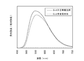
- FIG. 2 shows the emission spectrum (solid line) of the Gd-free phosphor and the emission spectrum (dotted line) of the Gd-containing phosphor.
- the Gd-containing phosphor has a longer peak wavelength and dominant wavelength than the Gd-free phosphor.
- the chromaticity diagram of FIG. 1 shows the chromaticity coordinates of the phosphor not containing Gd as P and the chromaticity coordinates of the phosphor containing Gd as P ′.
- the reproducible chromaticity range when combined with a blue semiconductor light emitting element having an emission peak wavelength of 450 nm is from a straight line L to a dotted line L ′. It can be seen that the intersection with the region A is shifted from X to X ′. From this, in the region A, it is expected that the Gd-containing phosphor can realize a white light emitting device having higher visibility than the Gd-free phosphor.
- the Gd-containing phosphor has lower emission characteristics at high temperatures than the Gd-free phosphor phosphor.
- the measurement results will be described in detail.
- FIG. 3 is a schematic view showing an apparatus for measuring a change in the light emission characteristic of the phosphor due to a change in temperature condition (hereinafter, temperature characteristic).
- a sample setting opening 11 a is formed on the upper surface of the aluminum substrate 11.
- a thermocouple 12 and a planar heater 13 located immediately below the opening 11 a are embedded in the aluminum substrate 11.
- the thermocouple 12 and the planar heater 13 are connected to a temperature controller.
- a condensing lens 14 that emits excitation light and a light receiving quartz fiber 17 that receives light emitted from a phosphor are installed above the opening 11a.
- a xenon lamp as an excitation light source is connected to the condenser lens 14 via a quartz fiber 15 and a spectroscope 16a.
- a photomultiplier as a measuring instrument is connected to the light receiving quartz fiber 17 via a spectroscope 16b.
- each phosphor 18 to be a sample was filled in the opening 11a, and the filling surface was smoothed with a squeegee or the like.
- the output of the planar heater 13 is adjusted by the temperature controller, and the temperature of the aluminum substrate 11 that changes in accordance with the output is fed back to the temperature controller via the thermocouple 12, and the temperature of the aluminum substrate is set to a predetermined temperature. Maintained.
- the temperature of the aluminum substrate is regarded as the temperature of the phosphor 18, and after 10 minutes have passed since the temperature of the aluminum substrate reaches each temperature condition, the light of the xenon lamp (USHIO Inc .: UXL-150D-O) is used as the spectroscope.
- 16a Horiba: H-20UV
- the quartz fiber 17 for light reception and the spectrometer 16b (Horiba Seisakusho: H-20VIS) was measured with Photomaru (Hamamatsu Photonics: R955-07).
- FIG. 4 shows temperature characteristics of the Gd-containing phosphor and the Gd-free phosphor under 450 nm excitation.
- the vertical axis of the graph in FIG. 4 shows the integrated emission intensity under each temperature condition for each phosphor as a ratio with the integrated emission intensity under 30 ° C. as 100%.
- the Gd-containing phosphor and the Gd-free phosphor both have lower integrated emission intensity as the temperature conditions become higher, but the Gd-containing phosphor is less than the Gd-free phosphor.
- the retention rate is low.
- the Gd-free phosphor has a maintenance rate of about 80%, whereas the Gd-containing phosphor has a maintenance rate of about 50%, which is about 1.6 times. The above difference in emission intensity occurs.
- the Gd-containing phosphor is not suitable for use in a high-output white light emitting device with a large calorific value because it requires a large current.
- the present invention has been made in view of the above circumstances, and an object thereof is a white light emitting device using a semiconductor light emitting element and a phosphor that is efficiently excited by the light of the semiconductor light emitting element to emit light.
- a white light emitting device capable of emitting white light within a chromaticity stipulated range of a white light source used for a vehicular lamp at a high emission intensity and having good temperature characteristics that do not deteriorate the light emission characteristics even at high temperatures; And it aims at providing the vehicular lamp using this.
- the present inventors have made extensive research to solve the above problems, the general formula Sr x Ba y Si 2 O 2 N 2: phosphor represented by Eu 2+, the efficiency in the wavelength range of 370 ⁇ 480 nm It has been newly found that it is well excited and emits visible light containing a large amount of yellow component at a high emission intensity, and has good temperature characteristics that do not deteriorate the light emission characteristics even at high temperatures. Furthermore, the present inventors combine the phosphors represented by the above general formula, and two or more types of phosphors in the range where the ratio x / y of x to y in the general formula is different. Furthermore, the inventors have newly found that visible light having a high color rendering property can be obtained, and have completed the present invention by constituting a white light emitting device using these two or more phosphors.
- the white light-emitting device is a white light-emitting device used for a vehicle lamp, a semiconductor light-emitting element having an emission spectrum peak in a wavelength range of 370 to 480 nm, and the semiconductor light-emitting device.
- is excited by light emitted from the device comprises at least two or more phosphors to emit visible light, as the phosphor, the general formula Sr x Ba y Si 2 O 2 N 2: a phosphor represented by Eu 2+
- the ratio value x / y is in the range of 100/0 to 60/40, and the ratio value x / y is in the range of 45/55 to 5/95.
- a second phosphor is used for a vehicle lamp, a semiconductor light-emitting element having an emission spectrum peak in a wavelength range of 370 to 480 nm, and the semiconductor light-emitting device.
- is excited by light emitted from the device comprises at least two or more phosphors to emit visible light, as
- the first phosphor preferably has a ratio x / y of x to y in the general formula in the range of 100/0 to 70/30, and the second phosphor is More preferably, the ratio value x / y is in the range of 40/60 to 5/95.
- x in the general formula is in the range of 0.60 ⁇ x ⁇ 0.97
- y is in the range of 0 ⁇ y ⁇ 0.35
- x + y is in the range of x + y ⁇ 0.97
- x is in the range of 0.03 ⁇ x ⁇ 0.40
- y is in the range of 0.40 ⁇ y ⁇ 0.90
- x + y is in the range of x + y ⁇ 0.97.
- the first phosphor has an emission spectrum dominant wavelength in a wavelength range of 550 to 565 nm
- the second phosphor has an emission spectrum dominant wavelength in a wavelength range of 578 to 600 nm. Is more preferable.
- the first phosphor preferably has an emission spectrum peak wavelength in the wavelength range of 535 to 570 nm, and the second phosphor has an emission spectrum peak wavelength of 575 to 570 nm. More preferably, it is in the wavelength region of 610 nm.
- the dominant wavelength and half width of the combined spectrum of the first phosphor and the second phosphor are in the wavelength range of 565 to 580 nm in terms of the color rendering property of the white light emitting device, and the half width is 100 nm. The above is preferable.
- the first phosphor and the second phosphor are europium-activated orthosilicates prepared by first firing a mixture of SrCO 3 , BaCO 3 , SiO 2 and Eu 2 O 3 in a reducing atmosphere. It is preferable to produce the precursor by subjecting a mixture of the precursor, Si 3 N 4 and NH 4 Cl to secondary firing in a reducing atmosphere.
- the first phosphor and the second phosphor manufactured as described above can exhibit good green to orange light emission.
- the semiconductor light emitting device is not particularly limited as long as it has an emission spectrum peak in the wavelength range of 370 to 480 nm. From the viewpoint of the excitation wavelength range of the phosphor, the emission spectrum peak is from 430 nm to 430 nm. It is preferable to be in the wavelength region of 470 nm. Specifically, for example, an InGaN-based LED having good light emission characteristics in a wavelength region near 450 nm is preferably used for the semiconductor light emitting element.
- the vehicular lamp according to the second embodiment of the present invention is characterized by using the white light emitting device as a light source.
- the white light emitting device of the present invention can emit white light with high luminous intensity and high color rendering properties within a chromaticity regulation range of a white light source used for a vehicle lamp.
- the same effect can be obtained in a vehicular lamp using such a white light emitting device as a light source.
- FIG. 4 is a chromaticity diagram showing chromaticity coordinates of a Gd-free phosphor and a Gd-containing phosphor, and a reproducible chromaticity range of a white light emitting device using these phosphors. It is drawing which shows the emission spectrum (solid line) of Gd non-containing fluorescent substance, and the emission spectrum (dotted line) of Gd containing fluorescent substance. It is the schematic which shows the apparatus which measures the temperature characteristic of fluorescent substance. It is drawing which shows the temperature characteristic of Gd containing fluorescent substance and Gd non-containing fluorescent substance. It is a schematic sectional drawing of the white light-emitting device 20 which is embodiment of this invention. It is a figure which shows the excitation spectrum of the fluorescent substance 1.
- the emission spectrum (solid line) of an Example and the emission spectrum (dotted line) of the comparative example 1 are shown. It is a schematic sectional drawing which shows the light-emitting device at the time of measuring a temperature characteristic. It is a figure which shows the emission spectrum of an Example. It is a figure which shows the emission spectrum of a comparative example.
- FIG. 5 is a schematic sectional view of the white light emitting device 20 according to the embodiment of the present invention.
- a pair of electrodes 22 a (anode) and 22 b (cathode) are formed on a substrate 21.
- a semiconductor light emitting element 23 is fixed on the electrode 22 a by a mount member 24.
- the semiconductor light emitting element 23 and the electrode 22 a are energized by the mount member 24, and the semiconductor light emitting element 23 and the electrode 22 b are energized by the wire 25.
- a fluorescent layer 26 is formed on the semiconductor light emitting element 23.
- the substrate 21 is preferably formed of a material having no electrical conductivity but high thermal conductivity.
- a ceramic substrate aluminum nitride substrate, alumina substrate, mullite substrate, glass ceramic substrate, a glass epoxy substrate, or the like is used. be able to.
- the electrodes 22a and 22b are conductive layers formed of a metal material such as gold or copper.
- the semiconductor light-emitting element 23 is an example of a light-emitting element used in the white light-emitting device 20, and for example, an LED or LD that emits ultraviolet light or short-wavelength visible light can be used.
- Specific examples include InGaN-based compound semiconductors.
- the emission wavelength range of the InGaN-based compound semiconductor varies depending on the In content. When the In content is large, the emission wavelength becomes a long wavelength, and when it is small, the wavelength tends to be a short wavelength.
- the mounting member 24 is, for example, a conductive adhesive such as silver paste or gold-tin eutectic solder, and the lower surface of the semiconductor light emitting element 23 is fixed to the electrode 22a.
- the electrode 22a is electrically connected.
- the wire 25 is a conductive member such as a gold wire, and is joined to the upper surface side electrode of the semiconductor light emitting element 23 and the electrode 22b by, for example, ultrasonic thermocompression bonding, and electrically connects both.
- the phosphor layer 26 is prepared by preparing a phosphor paste in which a phosphor is mixed in a liquid or gel binder member, and then applying the phosphor paste on the upper surface of the semiconductor light emitting element 23. It can be formed by curing the binder member of the phosphor paste.
- a silicone resin or a fluorine resin can be used as the binder member.
- the first phosphor and the second phosphor used in the white light emitting device 20 of this embodiment, Sr x Ba y Si 2 O 2 N 2: is a phosphor represented by the general formula Eu 2+.
- the first phosphor and the second phosphor are prepared by calcining a mixed powder of SrCO 3 , BaCO 3 , SiO 2 , Eu 2 O 3 in a reducing atmosphere to produce europium-activated orthosilicate as a precursor. To make. This precursor can be pulverized, added with Si 3 N 4 and NH 4 Cl, and fired in a reducing atmosphere.
- the fluorescent layer 26 in addition to the first phosphor and the second phosphor, one or more kinds of phosphors having emission characteristics different from these can be mixed.
- the chromaticity of white light obtained from the white light emitting device can be adjusted by changing the blending amount of these phosphors.
- the phosphor layer 26 can be mixed with substances other than phosphors having various physical properties.
- the refractive index of the fluorescent layer 26 can be increased by mixing the fluorescent layer 26 with a material having a higher refractive index than that of a binder member such as a metal oxide, a fluorine compound, or a sulfide.
- a binder member such as a metal oxide, a fluorine compound, or a sulfide.
- the refractive index can be increased without reducing the transparency of the fluorescent layer 26 by making the particle size of the mixed substance nano-sized.
- white powder having an average particle size of about 0.3 to 2 ⁇ m, such as alumina, zirconia, or titanium oxide, can be mixed in the fluorescent layer 26 as a light scattering agent. Thereby, unevenness in luminance and chromaticity of the light emitting surface can be prevented.
- the semiconductor light emitting element 23 when a driving current is applied to the electrodes 22 a and 22 b, the semiconductor light emitting element 23 is energized, and the semiconductor light emitting element 23 emits light in a specific wavelength region including blue light toward the fluorescent layer 26. To do. A part of this light is used to excite the phosphor in the fluorescent layer 26, and the remaining light passes through the fluorescent layer 26 and is directly irradiated to the outside. The phosphor is excited by light from the semiconductor light emitting element 23 and emits light in a specific wavelength range.
- White light can be obtained by additively mixing the light from the semiconductor light emitting element 23 that has passed through the fluorescent layer 26 and the light emitted from the phosphor.
- the above-described white light emitting device 20 will be described in more detail below using examples of the light emitting device.
- description of the raw material of the following light-emitting device, a manufacturing method, the chemical composition of fluorescent substance, etc. does not limit this invention at all.
- ⁇ Phosphor 1> A phosphor represented by Sr 0.93 Si 2 O 2 N 2 : Eu 2+ 0.07 .
- Phosphor 1 is an example of the first phosphor, Sr x Ba y Si 2 O 2 N 2: represented by the general formula Eu 2+, the ratio of x with respect to y in the general formula values x / y Is a phosphor with 100/0.
- ⁇ Phosphor 2> A phosphor represented by Sr 0.05 Ba 0.75 Si 2 O 2 N 2 : Eu 2+ 0.2 .
- Phosphor 2 is an example of the second phosphor, Sr x Ba y Si 2 O 2 N 2: represented by the general formula Eu 2+, the ratio of x with respect to y in the general formula values x / y Is a phosphor with 5/75.
- the phosphor 2 was manufactured by first weighing 0.114 g of SrCO 3 , 2.277 g of BaCO 3 , 0.541 g of Eu 2 O 3, and 0.462 g of SiO 2 , and putting each raw material in an alumina mortar. The mixture was pulverized for about 20 minutes, and this mixture was put in an alumina crucible, covered, and calcined in a reducing atmosphere H 2 / N 2 (5/95) in an electric furnace at 1100 ° C. for 3 hours, and the precursor Sr 0.1 Ba 1 .5 SiO 4 : Eu 2+ 0.4 was obtained.
- the phosphor for reference is manufactured by first weighing 1.321 g of SrCO 3 , 1.766 g of BaCO 3 , 0.556 g of Eu 2 O 3 and 0.632 g of SiO 2, and putting each raw material in an alumina mortar. The mixture was pulverized for about 20 minutes, and this mixture was put in an alumina crucible, covered, and fired in a reducing atmosphere H 2 / N 2 (5/95), 1100 ° C. for 3 hours in an electric furnace, and the precursor Sr 0.85 Ba 0.85 SiO 4 : Eu 2+ 0.30 was obtained.
- a mixed phosphor was prepared by mixing the phosphor 1 and the phosphor 2 so that the weight ratio of the phosphor 1 and the phosphor 2 was 5: 6.
- FIG. 6 shows the excitation spectrum of phosphor 1
- FIG. 7 shows the excitation spectrum of phosphor 2
- FIG. 8 shows the excitation spectrum of the reference phosphor.
- the excitation spectrum peak broadly exists at 400 to 470 nm in any of the phosphors. From this, it can be seen that these phosphors are efficiently excited by the light of the semiconductor light emitting element having the emission spectrum peak in the wavelength range of 370 to 480 nm and can emit light.
- Table 2 shows the x / y values for phosphor 1, phosphor 2, and reference phosphor, and the chromaticity coordinates (cx, cy) and dominant wavelength (nm) of the emission spectrum of each phosphor under 450 nm excitation. Show. Note that the value of x / y, Sr x Ba y Si 2 O 2 N 2: the value of the ratio of x for y in each phosphor represented by the general formula Eu 2+, strontium in each phosphor It is the content ratio (molar ratio) of barium.
- the phosphor 1, phosphor 2, and the reference fluorescent substance, both Sr x Ba y Si 2 O 2 N 2: is a phosphor represented by the general formula Eu 2+, barium to strontium It can be seen that the content ratio increases in the order of phosphor 1, reference phosphor, and phosphor 2, and the peak wavelength of the emission spectrum accordingly becomes longer.
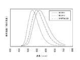
- FIG. 10 shows an emission spectrum (solid line) of phosphor 1 under excitation of 450 nm, an emission spectrum (dotted line) of phosphor 2, and an emission spectrum (dotted line) of the reference phosphor.
- shaft of the graph in FIG. 10 shows the relative light emission intensity
- the peak wavelength of the emission spectrum of each phosphor is in the wavelength range of 535 to 555 nm for phosphor 1, 560 to 580 nm for reference phosphor, and 575 to 595 nm for phosphor 2.
- the peak wavelength of the emission spectrum tends to shift to the longer wavelength side.
- the emission spectrum of each phosphor has no noticeable difference in waveform, and the half-value width is 80 to 110 for all.
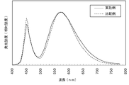
- FIG. 11 shows the emission spectrum (solid line) of the mixed phosphor 1 under 450 nm excitation and the emission spectrum (one-dot chain line) of the reference phosphor.
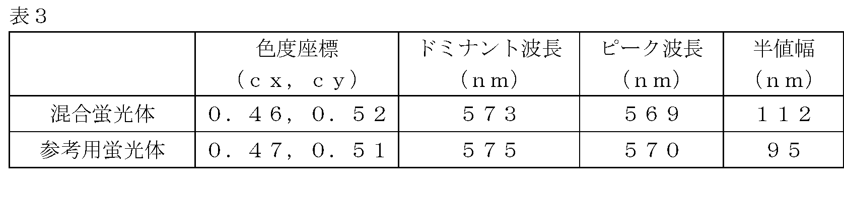
- Table 3 shows the chromaticity coordinates (cx, cy), the dominant wavelength (nm), the peak wavelength (nm), and the inverse width (nm) of the emission spectrum of each phosphor under 450 nm excitation.
- the emission spectra of the mixed phosphor and the reference phosphor are almost equal in terms of chromaticity coordinates, dominant wavelength, and peak wavelength, but the mixed phosphor is more in comparison with the reference phosphor. It can be seen that the emission spectrum has a broad half-value width and a broad emission spectrum containing a large amount of light in the wavelength range between the blue and yellow and in the red range.
- the chromaticity range that can be reproduced by additive mixing of a semiconductor light emitting device having an emission spectrum peak wavelength of 450 nm and each phosphor is the chromaticity coordinate point of the semiconductor light emitting device in the chromaticity diagram shown in FIG. It can be approximately represented by straight lines L1 to L4 connecting B and chromaticity coordinate points Y1 to Y4 of each phosphor.
- the straight lines L2 (reference phosphor), L3 (phosphor 2), and L4 (mixed phosphor) pass through the range of the region A, the chromaticity specification is satisfied by the combination with the blue light emitting semiconductor light emitting element. It is expected that white light can be emitted.
- the straight lines L2 and L4 pass almost in the middle of the region A, and the areas around the points X2 and X4 that are the intersections of the straight lines L2 and L4 and the yellow phosphor side boundary line of the region A are regions with high visibility. I understand that.
- the reference phosphor or the mixed phosphor can emit white light with high visibility in the region A by being combined with the blue light emitting semiconductor light emitting element.
- the mixed phosphor has a wider half-value width than the reference phosphor, and has more light in the wavelength region between the blue and yellow or in the red region. Since it has a broad emission spectrum including it, it is expected that the mixed phosphor can emit white light with higher visual sensitivity than the reference phosphor.
- the structure of the light-emitting device of an Example is explained in full detail.
- the structure of the following light-emitting device is a structure common to an Example and a comparative example except the kind of used fluorescent substance.
- the light emitting device of this example uses the following specific configuration in the above embodiment.
- an aluminum nitride substrate was used as the substrate 21, and an electrode 22a (anode) and an electrode 22b (cathode) were formed using gold on the surface.
- the semiconductor light emitting element 23 a 1 mm square LED having a light emission peak at 450 nm (SemiLEDs: MvpLED TM SL-V-B40AC) was used, and a silver paste dropped using a dispenser on the electrode 22a (anode). The lower surface of the LED was adhered onto (available from Able Stick: 84-1LMISR4), and the silver paste was cured at 175 ° C. for 1 hour.
- a ⁇ 45 ⁇ m gold wire was used as the wire 25, and this gold wire was bonded to the upper electrode of the LED and the electrode 22b (cathode) by ultrasonic thermocompression bonding.
- a silicone resin manufactured by Toray Dow Corning Silicone Co., Ltd .: JCR6140
- JCR6140 a 30 vol% phosphor paste in which various phosphors are mixed is prepared, and the phosphor paste is applied to the upper surface of the semiconductor light emitting device 23. did.
- the coating amount was applied while adjusting the film thickness so as to obtain a desired chromaticity.
- the phosphor layer 26 was formed by fixing the applied phosphor paste by step curing for 40 minutes in an 80 ° C. environment and then for 60 minutes in a 150 ° C. environment.
- Example> a phosphor paste was prepared using the mixed phosphor, and a light-emitting device was prepared using the phosphor paste, the coating amount being adjusted to approach point X4 in the chromaticity diagram of FIG.
- a phosphor paste was prepared using the reference phosphor, and a light emitting device was prepared by using the phosphor paste and adjusting the coating amount so as to approach point X2 in the chromaticity diagram of FIG. did.
- a phosphor paste was prepared using the Gd-containing phosphor (general formula (Y, Gd) 3 Al 5 O 12 : phosphor represented by Ce: manufactured by Kasei Optonics: P46-Y3).
- a light emitting device was manufactured and adjusted using the phosphor paste so that the coating amount was close to the point X ′ in the chromaticity diagram of FIG.
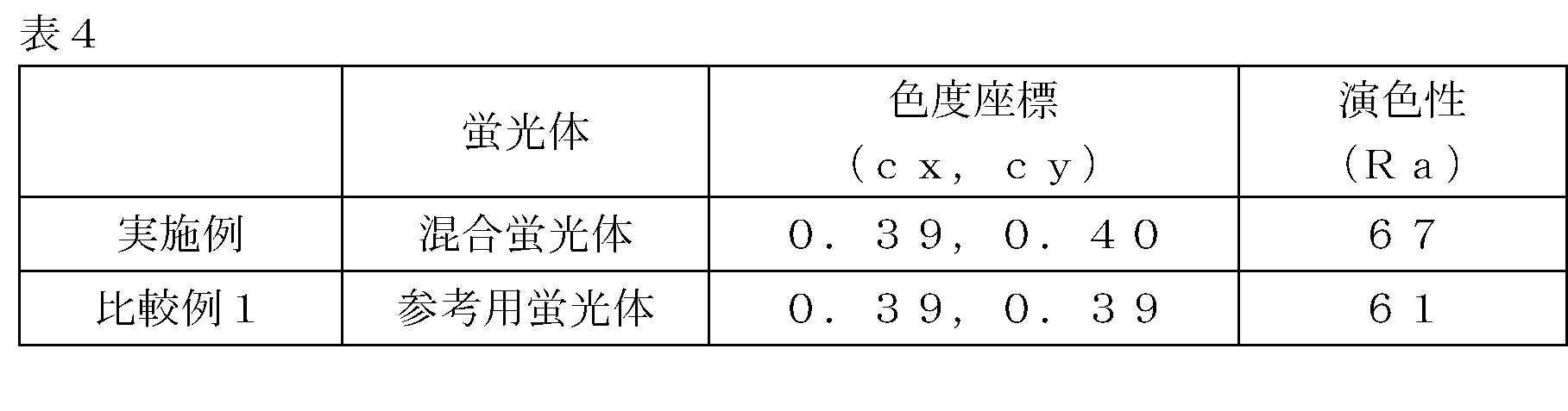
- Table 4 shows the integrated emission intensity ratio, chromaticity coordinates (cx, cy), and color rendering coefficient (Ra) when a driving current of 350 mA is applied to the example and the comparative example 1.
- FIG. 12 shows the emission spectrum (solid line) of the example and the emission spectrum (dotted line) of comparative example 1 when a driving current of 350 mA is applied to the example and comparative example 1.
- the chromaticity coordinates of any light-emitting device are in the region close to the phosphor side in the region A in the chromaticity diagram of FIG. It turns out that it is high white light. Furthermore, it can be seen from the values of color rendering properties in Table 4 and FIG. 12 that the example has a color rendering property higher than that of Comparative Example 1 and has a broad emission spectrum.
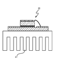
- the light emitting devices 20 of the example and the comparative example 2 are installed on the aluminum heat sink 27, and a driving current of 700 mA is applied to these light emitting devices. After being applied and allowed to stand in a thermostatic chamber at each ambient temperature for 15 minutes, the light emission intensity was measured with an instantaneous multi-photometry system (manufactured by Otsuka Electronics Co., Ltd .: MCPD-1000). The measurement results are shown below.
- Table 5 shows that the integrated luminescence intensity measured at ambient temperature is divided into the entire emission wavelength region (380 to 780 nm) of the light emitting device and the emission wavelength region (500 to 780 nm) of the phosphor. It is shown as a ratio where the integrated emission intensity under the condition of 100 ° C. is 100%.
- Example shows a higher maintenance rate than Comparative Example 2 for both the total emission wavelength region of the light emitting device and the emission wavelength region of the phosphor, and the Example has good temperature characteristics. I understand that.
- FIG. 14 shows an emission spectrum (solid line) under a 30 ° C. condition and a light emission spectrum (dotted line) under an 80 ° C. condition at a driving current of 700 mA for the light emitting device of the example.
- FIG. 15 shows an emission spectrum (solid line) under a 30 ° C. condition and a light emission spectrum (dotted line) under an 80 ° C. condition at a driving current of 700 mA for the light emitting device of Comparative Example 2.
- the emission intensity of the emission spectrum of each light-emitting device is reduced by the temperature increase from 30 ° C. to 80 ° C., but the example has a higher fluorescence region than Comparative Example 2. It can be seen that it is maintained.
- the phosphor of the present invention has been described according to the embodiments. However, it is needless to say that the present invention is not limited to these embodiments, and various modifications, improvements, combinations, usage forms, and the like can be considered.
- the white light emitting device of the present invention can be used for a vehicular lamp having a white light source having a functional color, such as a head lamp, a fog lamp, a cornering lamp, a license plate lamp, a backup lamp, and a room lamp. Further, the white light emitting device of the present invention is a vehicular lamp that is a combination of a white light source and a color filter, and can be used for a functional color other than a white system, for example, a tail lamp, a stop lamp, a turn signal lamp, or the like. .
Landscapes
- Chemical & Material Sciences (AREA)
- Inorganic Chemistry (AREA)
- Engineering & Computer Science (AREA)
- Materials Engineering (AREA)
- Organic Chemistry (AREA)
- Luminescent Compositions (AREA)
- Led Device Packages (AREA)
Abstract
発光素子とこの半導体発光素子の光で効率よく励起され発光する蛍光体を用いた白色発光装置であって、車両用灯具に用いられる白色光源の色度規定の範囲内にある視感度の高い白色光を高い発光強度且つ高い演色性で発光可能な白色発光装置、及びこれを用いた車両用灯具を提供することを目的としている。 車両用灯具に用いられる白色発光装置、及びこれを用いた車両用灯具であって、前記白色発光装置は、370~480nmの波長域に発光スペクトルのピークを持つ半導体発光素子と、前記半導体発光素子の発する光により励起され可視光を発光する少なくとも2種以上の蛍光体を備え、前記蛍光体は、SrxBaySi2O2N2:Eu2+の一般式で表され、前記一般式におけるyに対するxの比の値x/yが100/0~60/40の範囲内にある第一の蛍光体と、前記比の値x/yが45/55~5/95の範囲内にある第二の蛍光体とを備えることを特徴とする。
Description
本発明は、車両用灯具に用いられる白色発光装置、及びこれを用いた車両用灯具に関する。より詳しくは、半導体発光素子とこの半導体発光素子の光で効率よく励起され発光する蛍光体を用いて、車両用灯具に用いられる白色光源の色度規定の範囲内にある視感度の高い白色光を高い発光強度及び高い演色性で発光可能な白色発光装置、及びこれを用いた車両用灯具に関する。
近年、長寿命且つ消費電力が少ない白色発光装置として、青色光を発光する発光ダイオード(LED)やレーザダイオード(LD)等の半導体発光素子と、これらを励起光源とする蛍光体とを組み合わせ、両者から得られる発光の加色混合による合成スペクトルとして白色光を得るように構成された白色発光装置が注目されており、その用途として、車両用灯具、特に車両用前照灯の白色光源としての利用が期待されている。(特許文献1参照)
ここで、車両用灯具の白色光源は、色度規定により発光スペクトルが所定の色度座標(cx,cy)の範囲内にあることが要求されており、例えば、JIS:D5500によれば、図1の色度図に示す領域Aの範囲内にあることが要求される。
尚、領域Aは下記式によって表される。
<車両用前照灯の白色光源の色度規定(JIS:D5500)>
黄色方向 cx≦0.50
青色方向 cx≧0.31
緑色方向 cy≦0.44 及び cy≦0.15+0.64cx
紫色方向 cy≧0.05+0.75cx 及び cy≧0.382
ここで、車両用灯具の白色光源は、色度規定により発光スペクトルが所定の色度座標(cx,cy)の範囲内にあることが要求されており、例えば、JIS:D5500によれば、図1の色度図に示す領域Aの範囲内にあることが要求される。
尚、領域Aは下記式によって表される。
<車両用前照灯の白色光源の色度規定(JIS:D5500)>
黄色方向 cx≦0.50
青色方向 cx≧0.31
緑色方向 cy≦0.44 及び cy≦0.15+0.64cx
紫色方向 cy≧0.05+0.75cx 及び cy≧0.382
このような色度規定に合致した白色光を高い発光強度で発光可能とした白色発光装置の例として、青色波長域(420~490nm)に発光ピーク波長を持つInGaN系の半導体発光素子と、510~600nmの間に発光ピーク波長を持つセリウム付活のイットリウム・アルミニウム・ガーネット(YAG)系の黄色蛍光体とを組み合わせて白色発光を実現する白色発光装置が知られている。(特許文献2参照)
日本国特許出願公開2004-095480号公報
日本国特許第3503139号公報
ところで、青色光を発光する半導体発光素子と黄色蛍光体とを組み合わせた白色発光装置が再現可能な色度範囲は、半導体発光素子が発光する青色光の色度座標と蛍光体の発光する黄色光の色度座標とを結んだ直線により近似的に表すことができ、両者の発光強度を調整することで当該直線上における任意の色度座標の光を得ることができる。
図1の色度図に示す直線Lは、このような直線の一例であり、発光ピーク波長が450nmの青色半導体発光素子と色度座標がP(cx=0.43,cy=0.54)である黄色蛍光体とを組み合わせた白色発光装置によって再現可能な色度範囲を示す直線である。
図1の色度図に示す直線Lは、このような直線の一例であり、発光ピーク波長が450nmの青色半導体発光素子と色度座標がP(cx=0.43,cy=0.54)である黄色蛍光体とを組み合わせた白色発光装置によって再現可能な色度範囲を示す直線である。
ここで、人の目が明るさを感じる視感度は、青色光に比べ黄色光は約20倍高いことから、青色光と黄色光を加色混合した白色光の場合、同じ発光強度であっても黄色光成分が多い白色光のほうが人の目には明るく感じられる。このことは、前記直線L上の各色度座標の光は、同じ発光強度であれば黄色蛍光体側に近い方が人の目に明るく感じられることを示す。また、前記領域A(車両用灯具の白色光源の色度規定)の範囲内において最も視感度が高い色度座標は領域Aの黄色蛍光体側境界線と前記直線Lの交差点Xとなる。
従って、前記領域A(車両用灯具の白色光源の色度規定)の範囲内において白色光の視感度の高さを追求すると、交差点Xの座標がより黄色蛍光体側(図1中のX’側)へと近くなるように半導体発光素子の発光色と蛍光体の発光色を選択する必要がある。
具体的には、半導体発光素子の発光ピーク波長を450nm前後とした場合に、前記交差点Xの座標が視感度の高い範囲となるのは、黄色蛍光体のドミナント波長が575nm~590nmの範囲である。
具体的には、半導体発光素子の発光ピーク波長を450nm前後とした場合に、前記交差点Xの座標が視感度の高い範囲となるのは、黄色蛍光体のドミナント波長が575nm~590nmの範囲である。
しかし、従来知られた青色光を発光する半導体発光素子とYAG系蛍光体を組み合わせた白色発光装置においては、ドミナント波長が575nm~590nmの範囲内において高い発光強度が得られるYAG系蛍光体が知られていないため、視感度の高い白色光を高い発光強度で発光可能な白色発光装置の実現が困難であった。
尚、前記YAG系の黄色蛍光体においては、ガドリニウムを混合することにより発光スペクトルのドミナント波長が長波長側へシフトすることが知られている。
そこで、発明者らは、ガドリニウムを含有していない一般式Y3Al5O12:Ceで表されるYAG系蛍光体(Phosphor Technology社(英)製:QUM58/F-U1、以下Gd非含有蛍光体)と、このYAG系蛍光体にガドリニウムを混入した一般式(Y,Gd)3Al5O12:Ceで表される蛍光体(化成オプトニクス社製: P46-Y3、以下Gd含有蛍光体)について、これらの蛍光体の発光特性を測定したところ、下記の結果が得られた。
そこで、発明者らは、ガドリニウムを含有していない一般式Y3Al5O12:Ceで表されるYAG系蛍光体(Phosphor Technology社(英)製:QUM58/F-U1、以下Gd非含有蛍光体)と、このYAG系蛍光体にガドリニウムを混入した一般式(Y,Gd)3Al5O12:Ceで表される蛍光体(化成オプトニクス社製: P46-Y3、以下Gd含有蛍光体)について、これらの蛍光体の発光特性を測定したところ、下記の結果が得られた。
表1に、450nm励起下における各蛍光体の色度座標(cx,cy)、ピーク波長(nm)、及びドミナント波長(nm)を示す。

また、図2は、Gd非含有蛍光体の発光スペクトル(実線)、及びGd含有蛍光体の発光スペクトル(点線)を示す。
表1及び図2に示すように、Gd含有蛍光体は、Gd非含有蛍光体に対して、ピーク波長とドミナント波長がいずれも長波長である。
図1の色度図は、Gd非含有蛍光体の色度座標をPとして、Gd含有蛍光体の色度座標をP´として示したものである。
この図1の色度座標から、色度座標がPからP´へシフトすると、発光ピーク波長が450nmの青色半導体発光素子と組み合わせた場合に再現可能な色度範囲は直線Lから点線L´へ、前記領域Aとの交差点はXからX´へとそれぞれシフトすることが分かる。
このことから、前記領域A内において、Gd含有蛍光体はGd非含有蛍光体よりも視感度の高い白色発光装置を実現可能であることが予想される。
この図1の色度座標から、色度座標がPからP´へシフトすると、発光ピーク波長が450nmの青色半導体発光素子と組み合わせた場合に再現可能な色度範囲は直線Lから点線L´へ、前記領域Aとの交差点はXからX´へとそれぞれシフトすることが分かる。
このことから、前記領域A内において、Gd含有蛍光体はGd非含有蛍光体よりも視感度の高い白色発光装置を実現可能であることが予想される。
しかし、本発明者らの測定結果によれば、前記Gd含有蛍光体は、前記Gd非含有蛍光体蛍光体に比べて、高温下における発光特性が低いことが分かった。
以下、その測定結果を詳述する。
以下、その測定結果を詳述する。
図3は、温度条件の変化による蛍光体の発光特性の変化(以下、温度特性)を測定する装置を示す概略図である。
図3に示す測定装置10において、アルミ基板11の上面にはサンプルセット用の開口部11aが形成されている。また、アルミ基板11の内部には開口部11aの直下に位置する熱電対12及び面状ヒーター13が埋設されている。また、これらの熱電対12及び面状ヒーター13は温度コントローラーに接続されている。
図3に示す測定装置10において、アルミ基板11の上面にはサンプルセット用の開口部11aが形成されている。また、アルミ基板11の内部には開口部11aの直下に位置する熱電対12及び面状ヒーター13が埋設されている。また、これらの熱電対12及び面状ヒーター13は温度コントローラーに接続されている。
開口部11aの上方には励起光を出射する集光レンズ14と、蛍光体の発光を受光する受光用石英ファイバー17が設置されている。集光レンズ14には、励起光源としてのキセノンランプが石英ファイバー15及び分光器16aを介して接続されている。受光用石英ファイバー17には、計測器としてのフォトマルが分光器16bを介して接続されている。
上記のように構成された測定装置10において、各蛍光体の温度特性を下記の通り測定した。まず、サンプルとなる各蛍光体18を開口部11aに充填し、充填表面をスキージ等で平滑面とした。次に、温度コントローラーにより面状ヒーター13の出力を調整し、その出力に応じて変化するアルミ基板11の温度を熱電対12を介して温度コントローラーにフィードバックし、アルミ基板の温度を所定の温度で維持した。
このアルミ基板の温度を蛍光体18の温度と見なし、アルミ基板の温度が各温度条件に達してから10分経過した後に、キセノンランプ(ウシオ電機製:UXL-150D-O)の光を分光器16a(堀場製作所製:H-20UV)を介して450nmに分光した光を集光レンズ14より励起光として蛍光体18に照射し、発光した蛍光体の光を受光用石英ファイバー17及び分光器16b(堀場製作所:H-20VIS)を介してフォトマル(浜松ホトニクス製:R955-07)で測定した。
図4は、450nm励起下における前記Gd含有蛍光体及び前記Gd非含有蛍光体の温度特性を示す。図4におけるグラフの縦軸は、それぞれの蛍光体について、各温度条件下における積分発光強度を、30℃条件下における積分発光強度を100%とする比率として示したものである。
図4に示すように、前記Gd含有蛍光体及び前記Gd非含有蛍光体は、いずれも温度条件が高温になるに従って積分発光強度が低下するが、Gd含有蛍光体はGd非含有蛍光体に比べてその維持率が低く、200℃条件下においては、Gd非含有蛍光体が80%程度の維持率であるのに対しGd含有蛍光体は50%程度の維持率であり、約1.6倍以上の発光強度の差が生じている。
以上より、Gd含有蛍光体はガドリニウムの影響により発光スペクトルのドミナント波長が長波長側へシフトするが、高温下における発光特性は低下する。したがって、Gd含有蛍光体は、大電流を必要とするため発熱量が大きい高出力の白色発光装置での利用には向いていなかった。
また、従来知られた青色光を発光する半導体発光素子とYAG系蛍光体を組み合わせた白色発光装置においては、青色と黄色の中間の波長領域の光、及び蛍光体から得られる赤色領域の光が少ないことから、演色性が低いという問題があった。
本発明は、上記のような事情を鑑みてなされたものであり、その目的は、半導体発光素子とこの半導体発光素子の光で効率よく励起され発光する蛍光体を用いた白色発光装置であって、車両用灯具に用いられる白色光源の色度規定の範囲内にある白色光を高い発光強度で発光可能であり、且つ高温下においても発光特性が低下しない良好な温度特性を有する白色発光装置、及びこれを用いた車両用灯具を提供することを目的としている。
本発明者らは、上記課題を解決すべく研究を重ねた結果、一般式がSrxBaySi2O2N2:Eu2+で表される蛍光体は、370~480nmの波長域で効率良く励起され、黄色成分を多く含む可視光を高い発光強度で発光すること、及び高温下においても発光特性が低下しない良好な温度特性を有することを新たに見出した。
さらに、本発明者らは、前記一般式で表される蛍光体であって、前記一般式におけるyに対するxの比の値x/yが異なる範囲にある2種類以上の蛍光体を組み合わせることにより、さらに演色性が高い可視光を得られることを新たに見出し、これら2種以上の蛍光体を用いて白色発光装置を構成することで本発明を完成するに至った。
さらに、本発明者らは、前記一般式で表される蛍光体であって、前記一般式におけるyに対するxの比の値x/yが異なる範囲にある2種類以上の蛍光体を組み合わせることにより、さらに演色性が高い可視光を得られることを新たに見出し、これら2種以上の蛍光体を用いて白色発光装置を構成することで本発明を完成するに至った。
すなわち、本発明の第1の形態である白色発光装置は、車両用灯具に用いられる白色発光装置であって、370~480nmの波長域に発光スペクトルのピークを持つ半導体発光素子と、前記半導体発光素子の発する光により励起され可視光を発光する少なくとも2種以上の蛍光体を備え、前記蛍光体として、一般式SrxBaySi2O2N2:Eu2+で表される蛍光体であって、前記比の値x/yが100/0~60/40の範囲内にある第一の蛍光体と、前記比の値x/yが45/55~5/95の範囲内にある第二の蛍光体とを備えることを特徴とする。
また、前記第一の蛍光体は、前記一般式におけるyに対するxの比の値x/yが100/0~70/30の範囲内にあることがより好ましく、前記第二の蛍光体は、前記比の値x/yが40/60~5/95の範囲内にあることがより好ましい。このような第一の蛍光体及び第二の蛍光体を用いることにより、さらに良好な演色性を確保することができる。
また、前記第一の蛍光体は、前記一般式のxが0.60<x<0.97、yが0≦y<0.35、x+yはx+y<0.97の範囲であることがより好ましく、前記第二の蛍光体は、xが0.03<x<0.40、yが0.40<y<0.90、x+yはx+y<0.97の範囲であることがより好ましい。このような第一の蛍光体及び第二の蛍光体を用いることにより、発光効率をさらに向上させることができる。
前記第一の蛍光体は、発光スペクトルのドミナント波長が550~565nmの波長域にあることがより好ましく、前記第二の蛍光体は、発光スペクトルのドミナント波長が578~600nmの波長域にあることがより好ましい。このような第一の蛍光体及び第二の蛍光体を用いることにより、視感度が高く、色温度3000K~4000Kの暖色系の白色光を発光する白色発光装置を得ることができる。
また、同様の理由により、前記第一の蛍光体は、発光スペクトルのピーク波長が535~570nmの波長域にあることがより好ましく、前記第二の蛍光体は、発光スペクトルのピーク波長が575~610nmの波長域にあることがより好ましい。
前記第一の蛍光体及び前記第二の蛍光体の合成スペクトルのドミナント波長及び半値幅は、白色発光装置の演色性の観点から、ドミナント波長が565~580nmの波長域にあり、半値幅が100nm以上であることが好ましい。
前記第一の蛍光体及び前記第二の蛍光体は、SrCO3、BaCO3、SiO2及びEu2O3の混合物を還元雰囲気中で1次焼成して作製したユーロピウム付活のオルソ珪酸塩を前駆体とし、この前駆体とSi3N4及びNH4Clの混合物を還元雰囲気中で2次焼成することにより製造されることが好ましい。このように製造された前記第一の蛍光体及び前記第二の蛍光体は、良好な緑~橙色の発光を示すことができる。
上記半導体発光素子は、370~480nmの波長域に発光スペクトルのピークを持つものであれば特に限定されるものではないが、前記蛍光体の励起波長域の観点から、発光スペクトルのピークが430nm~470nmの波長域にあることが好ましい。具体的には、上記半導体発光素子には、例えば、450nm付近の波長域の発光特性が良好であるInGaN系LEDが好ましく用いられる。
本発明の第2の形態である車両用灯具は、上記の白色発光装置を光源として用いることを特徴とする。
本発明の白色発光装置は、車両用灯具に用いられる白色光源の色度規定の範囲内にある視感度の高い白色光を高い発光強度且つ高い演色性で発光することができる。また、このような白色発光装置を光源として用いた車両用灯具においても、同様の効果を奏する。
10:測定装置
11:アルミ基板
11a:開口部
12:熱電対
13:面状ヒーター
14:集光レンズ
15:石英ファイバー
16a、16b:分光器
17:受光用石英ファイバー
18:蛍光体
20:白色発光装置
21:基板
22a:電極(陽極)
22b:電極(陰極)
23:半導体発光素子
24:マウント部材
25:ワイヤー
26:蛍光層
27:ヒートシンク
11:アルミ基板
11a:開口部
12:熱電対
13:面状ヒーター
14:集光レンズ
15:石英ファイバー
16a、16b:分光器
17:受光用石英ファイバー
18:蛍光体
20:白色発光装置
21:基板
22a:電極(陽極)
22b:電極(陰極)
23:半導体発光素子
24:マウント部材
25:ワイヤー
26:蛍光層
27:ヒートシンク
以下、本発明の実施の形態について図面を参照して説明する。なお、本発明は、以下の説明における例示などによって何ら限定されるものではない。
図5は、本発明の実施形態である白色発光装置20の概略断面図である。図5に示すように、白色発光装置20は、基板21上に一対の電極22a(陽極)及び22b(陰極)が形成されている。電極22a上には半導体発光素子23がマウント部材24により固定されている。半導体発光素子23と電極22aは前記マウント部材24により通電されており、半導体発光素子23と電極22bはワイヤー25により通電されている。半導体発光素子23の上には蛍光層26が形成されている。
基板21は、導電性を有しないが熱伝導性は高い材料によって形成されることが好ましく、例えば、セラミック基板(窒化アルミニウム基板、アルミナ基板、ムライト基板、ガラスセラミック基板)やガラスエポキシ基板等を用いることができる。
電極22a及び22bは、金や銅等の金属材料によって形成された導電層である。
半導体発光素子23は、白色発光装置20に用いられる発光素子の一例であり、例えば、紫外線又は短波長可視光を発光するLEDやLD等を用いることができる。具体例として、InGaN系の化合物半導体を挙げることができる。InGaN系の化合物半導体は、Inの含有量によって発光波長域が変化する。Inの含有量が多いと発光波長が長波長となり、少ない場合は短波長となる傾向を示す。
マウント部材24は、例えば銀ペースト等の導電性接着材または金錫共晶はんだ等であり、半導体発光素子23の下面を電極22aに固定し、半導体発光素子23の下面側電極と基板21上の電極22aを電気的に接続する。
ワイヤー25は、金ワイヤー等の導電部材であり、例えば超音波熱圧着等により半導体発光素子23の上面側電極及び電極22bに接合され、両者を電気的に接続する。
蛍光層26には、後述する蛍光体がバインダー部材によって半導体発光素子23の上面を覆う膜状に封止されている。このような蛍光層26は、例えば、液状又はゲル状のバインダー部材に蛍光体を混入した蛍光体ペーストを作製した後、当該蛍光体ペーストを半導体発光素子23の上面に塗布し、その後に塗布した蛍光体ペーストのバインダー部材を硬化することにより形成することができる。バインダー部材としては、例えば、シリコーン樹脂やフッ素樹脂等を用いることができる。
本実施形態の白色発光装置20に用いられる第一の蛍光体及び第二の蛍光体は、SrxBaySi2O2N2:Eu2+の一般式で表される蛍光体である。この第一の蛍光体及び第二の蛍光体は、例えば、SrCO3、BaCO3、SiO2、Eu2O3の混合粉末を還元雰囲気中で焼成し、ユーロピウム付活のオルソ珪酸塩を前駆体として作製する。この前駆体を粉砕し、Si3N4とNH4Clを加え、還元雰囲気中で焼成することで得ることができる。
蛍光層26には、上記第一の蛍光体及び第二の蛍光体に加え、これらとは異なる発光特性を有する1種又は複数種類の蛍光体を混入することができる。これらの蛍光体の配合量を変化させることにより白色発光装置から得られる白色光の色度を調整することができる。
また、蛍光層26には、種々の物性を有する蛍光体以外の物質を混入することもできる。例えば、金属酸化物、フッ素化合物、硫化物等のバインダー部材よりも屈折率の高い物質を蛍光層26に混入することにより、蛍光層26の屈折率を高めることができる。これにより、半導体発光素子4から発生する光が蛍光層26入射する際に生ずる全反射を低減させ、蛍光層26への励起光の取り込み効率を向上させるという効果が得られる。更に、混入する物質の粒子径をナノサイズにすることで、蛍光層26の透明度を低下させることなく屈折率を高めることができる。
また、アルミナ、ジルコニア、酸化チタン等の平均粒径0.3~2μm程度の白色粉末を光散乱剤として蛍光層26に混入することもできる。これにより、発光面の輝度、色度むらを防止することができる。
また、アルミナ、ジルコニア、酸化チタン等の平均粒径0.3~2μm程度の白色粉末を光散乱剤として蛍光層26に混入することもできる。これにより、発光面の輝度、色度むらを防止することができる。
上記白色発光装置20において、電極22a、22bに対し駆動電流を印加すると、半導体発光素子23が通電され、半導体発光素子23は蛍光層26へ向けて青色光を含む固有の波長域の光を照射する。この光の一部は蛍光層26内の蛍光体の励起に用いられ、残りの光は蛍光層26を透過してそのまま外部へと照射される。蛍光体は半導体発光素子23からの光により励起され固有の波長域の光を照射する。蛍光層26を透過した半導体発光素子23からの光と蛍光体が発する光を加色混合することにより白色光を得ることができる。
上記の白色発光装置20について、以下において、発光装置の実施例を用いて更に具体的に説明する。なお、下記の発光装置の原料、製造方法、蛍光体の化学組成等の記載は本発明を何ら限定するものではない。
まず、本実施例の発光装置において用いた蛍光体について詳述する。
<蛍光体1>
Sr0.93Si2O2N2:Eu2+ 0.07で表される蛍光体。
Sr0.93Si2O2N2:Eu2+ 0.07で表される蛍光体。
本蛍光体1は前記第一の蛍光体の一例であり、SrxBaySi2O2N2:Eu2+の一般式で表され、当該一般式におけるyに対するxの比の値x/yを100/0とした蛍光体である。
本蛍光体1の製造は、まず、SrCO3を3.051g、Eu2O3を0.0274g、SiO2を0.668gそれぞれ秤量し、各原料をアルミナ乳鉢に入れ約20分混合粉砕し、この混合物をアルミナ坩堝に入れ蓋をし、還元雰囲気H2/N2(5/95)、1100℃の電気炉で3時間焼成し、前駆体Sr1.86SiO4:Eu2+
0.14を得た。
次に、上記前駆体を2.763g、Si3N4を1.403g、NH4Clをフラックスとして0.04gそれぞれ秤量し、各原料をアルミナ乳鉢に入れ約20分混合粉砕し、この混合物をアルミナ坩堝に入れ蓋をし、還元雰囲気H2/N2(5/95)、1200~1400℃で6時間焼成し、蛍光体1を得た。
<蛍光体2>
Sr0.05Ba0.75Si2O2N2:Eu2+ 0.2で表される蛍光体。
Sr0.05Ba0.75Si2O2N2:Eu2+ 0.2で表される蛍光体。
本蛍光体2は前記第二の蛍光体の一例であり、SrxBaySi2O2N2:Eu2+の一般式で表され、当該一般式におけるyに対するxの比の値x/yを5/75とした蛍光体である。
本蛍光体2の製造は、まず、SrCO3を0.114g、BaCO3を2.277g、Eu2O3を0.541g、SiO2を0.462gそれぞれ秤量し、各原料をアルミナ乳鉢に入れ約20分混合粉砕し、この混合物をアルミナ坩堝に入れ蓋をし、還元雰囲気H2/N2(5/95)、1100℃の電気炉で3時間焼成し、前駆体Sr0.1Ba1.5SiO4:Eu2+
0.4を得た。
次に、上記前駆体を2.451g、Si3N4を0.935g、NH4Clをフラックスとして0.034gそれぞれ秤量し、各原料をアルミナ乳鉢に入れ約20分混合粉砕し、この混合物をアルミナ坩堝に入れ蓋をし、還元雰囲気H2/N2(5/95)、1200~1400℃で6時間焼成し、蛍光体2を得た。
<参考用蛍光体>
参考用蛍光体として、Sr0.425Ba0.425Si2O2N2:Eu2+ 0.15で表される蛍光体を作製した。
参考用蛍光体として、Sr0.425Ba0.425Si2O2N2:Eu2+ 0.15で表される蛍光体を作製した。
この参考用蛍光体は、SrxBaySi2O2N2:Eu2+の一般式で表され、当該一般式におけるyに対するxの比の値x/yを50/50とした蛍光体である。
この参考用蛍光体の製造は、まず、SrCO3を1.321g、BaCO3を1.766g、Eu2O3を0.556g、SiO2を0.632gそれぞれ秤量し、各原料をアルミナ乳鉢に入れ約20分混合粉砕し、この混合物をアルミナ坩堝に入れ蓋をし、還元雰囲気H2/N2(5/95)、1100℃の電気炉で3時間焼成し、前駆体Sr0.85Ba0.85SiO4:Eu2+
0.30を得た。
次に、上記前駆体を3.289g、Si3N4を1.403g、NH4Clをフラックスとして0.047gそれぞれ秤量し、各原料をアルミナ乳鉢に入れ約20分混合粉砕し、この混合物をアルミナ坩堝に入れ蓋をし、還元雰囲気H2/N2(5/95)、1200~1400℃で6時間焼成し、参考用蛍光体を得た。
<混合蛍光体>
前記蛍光体1及び前記蛍光体2を、これらの重量比が蛍光体1:蛍光体2=5:6となるように混合した混合蛍光体を作製した。
前記蛍光体1及び前記蛍光体2を、これらの重量比が蛍光体1:蛍光体2=5:6となるように混合した混合蛍光体を作製した。
<蛍光体の発光特性の評価結果>
以下、蛍光体1、蛍光体2、参考用蛍光体、及び混合蛍光体について測定した450nm励起下における各種の発光特性を詳述する。
以下、蛍光体1、蛍光体2、参考用蛍光体、及び混合蛍光体について測定した450nm励起下における各種の発光特性を詳述する。
図6に蛍光体1の励起スペクトルを、図7に蛍光体2の励起スペクトルを、図8に参考用蛍光体の励起スペクトルをそれぞれ示す。
図6~8から、いずれの蛍光体も励起スペクトルのピークが400~470nmにブロードに存在することが分かる。
このことから、これらの蛍光体は、370~480nmの波長域に発光スペクトルのピークを持つ半導体発光素子の光により効率良く励起され、発光可能であることが分かる。
このことから、これらの蛍光体は、370~480nmの波長域に発光スペクトルのピークを持つ半導体発光素子の光により効率良く励起され、発光可能であることが分かる。
表2に、蛍光体1、蛍光体2、参考用蛍光体に関するx/yの値、並びに各蛍光体の450nm励起下における発光スペクトルの色度座標(cx,cy)及びドミナント波長(nm)を示す。
尚、x/yの値とは、SrxBaySi2O2N2:Eu2+の一般式で表される各蛍光体におけるyに対するxの比の値であり、各蛍光体におけるストロンチウムとバリウムの含有比率(モル比)である。

尚、x/yの値とは、SrxBaySi2O2N2:Eu2+の一般式で表される各蛍光体におけるyに対するxの比の値であり、各蛍光体におけるストロンチウムとバリウムの含有比率(モル比)である。
この表2から、蛍光体1、蛍光体2、及び参考用蛍光体は、いずれもSrxBaySi2O2N2:Eu2+の一般式で示される蛍光体であるが、ストロンチウムに対するバリウムの含有比率は、蛍光体1、参考用蛍光体、蛍光体2の順序で大きくなり、それに応じて発光スペクトルのピーク波長が長波長となることが分かる。
図9の色度図に、各蛍光体の色度座標Y1~Y3と発光スペクトルのピークが450nmである半導体発光素子の色度座標B(cx=0.152、cy=0.025)を示す。
この図9の色度図から、Y1~Y3は仮想の直線である点線D上にほぼ並んで位置していることがわかる。
このことから、SrxBaySi2O2N2:Eu2+の一般式で示される蛍光体の色度座標は、前記点線D上において前記一般式におけるyに対するxの比の値x/yの値に応じたいずれかの地点に位置し、前記比の値x/yの値が100/0~60/40の範囲内にある前記第一の蛍光体はY2よりもY1側に位置し、前記比の値x/yの値が45/55~5/95の範囲内にある前記第二の蛍光体はY2よりもY3側に位置することが予想される。
このことから、SrxBaySi2O2N2:Eu2+の一般式で示される蛍光体の色度座標は、前記点線D上において前記一般式におけるyに対するxの比の値x/yの値に応じたいずれかの地点に位置し、前記比の値x/yの値が100/0~60/40の範囲内にある前記第一の蛍光体はY2よりもY1側に位置し、前記比の値x/yの値が45/55~5/95の範囲内にある前記第二の蛍光体はY2よりもY3側に位置することが予想される。
図10は、450nm励起下における蛍光体1の発光スペクトル(実線)、蛍光体2の発光スペクトル(点線)、及び参考用蛍光体の発光スペクトル(一点鎖線)を示す。
尚、図10におけるグラフの縦軸は各蛍光体の相対的な発光強度を示すものである。
尚、図10におけるグラフの縦軸は各蛍光体の相対的な発光強度を示すものである。
図10に示すように、各蛍光体の発光スペクトルのピーク波長は、蛍光体1が535~555nm、参考用蛍光体が560~580nm、蛍光体2が575~595nmの波長域にあり、ストロンチウムに対するバリウム含有比率(モル比)が大きい蛍光体ほど、発光スペクトルのピーク波長が長波長側へシフトする傾向がある。また、図10に示すように、各蛍光体の発光スペクトルは、波形においては目立った違いが無く、いずれも半値幅は80~110である。
図11は、450nm励起下における混合蛍光体1の発光スペクトル(実線)及び参考用蛍光体の発光スペクトル(一点鎖線)を示す。
また、表3は、450nm励起下における各蛍光体の発光スペクトルの色度座標(cx,cy)、ドミナント波長(nm)、ピーク波長(nm)、及び反値幅(nm)を示す。
また、表3は、450nm励起下における各蛍光体の発光スペクトルの色度座標(cx,cy)、ドミナント波長(nm)、ピーク波長(nm)、及び反値幅(nm)を示す。
図11及び表3に示すように、混合蛍光体と参考用蛍光体の発光スペクトルは、色度座標、ドミナント波長及びピーク波長についてはほぼ等しいが、混合蛍光体の方が参考用蛍光体に比べて半値幅が広く、青色と黄色の中間の波長領域や赤色領域の光を多く含むブロードな発光スペクトルをしていることが分かる。
<加色混合による白色光化の検討>
前述の通り、発光スペクトルのピーク波長が450nmである半導体発光素子と各蛍光体の加色混合によって再現可能な色度範囲は、図9に示す色度図における当該半導体発光素子の色度座標ポイントBと各蛍光体の色度座標ポイントY1~Y4とを結んだ直線L1~L4により近似的に表すことができる。
前述の通り、発光スペクトルのピーク波長が450nmである半導体発光素子と各蛍光体の加色混合によって再現可能な色度範囲は、図9に示す色度図における当該半導体発光素子の色度座標ポイントBと各蛍光体の色度座標ポイントY1~Y4とを結んだ直線L1~L4により近似的に表すことができる。
図9に示す色度図より、直線L1(蛍光体1)は車両用前照灯の白色光源の色度規定(JIS:D5500)の範囲を示す領域Aの範囲を通過しないため、蛍光体1を単独で青色発光の半導体発光素子と組み合わせた場合には、当該色度規定を満たす白色光の発光は不可能であることが予想される。
一方、直線L2(参考用蛍光体)、L3(蛍光体2)及びL4(混合蛍光体)は領域Aの範囲を通過するため、青色発光の半導体発光素子との組み合わせにより前記色度規定を満たす白色光の発光が可能であることが予想される。
特に、直線L2及びL4は領域Aのほぼ真中を通過しており、直線L2及びL4と領域Aの黄色蛍光体側境界線との交差点であるポイントX2及びX4の周辺は視感度の高い領域であることが分かる。
特に、直線L2及びL4は領域Aのほぼ真中を通過しており、直線L2及びL4と領域Aの黄色蛍光体側境界線との交差点であるポイントX2及びX4の周辺は視感度の高い領域であることが分かる。
このことから、参考用蛍光体又は混合蛍光体は、青色発光の半導体発光素子との組み合わせることにより、領域Aの範囲において視感度の高い白色光の発光が可能であることが予想される。
ここで、参考用蛍光体と混合蛍光体を比較した場合、上述の通り、混合蛍光体は参考用蛍光体よりも半値幅が広く、青色と黄色の中間の波長領域や赤色領域の光を多く含むブロードな発光スペクトルをしていることから、混合蛍光体は参考用蛍光体よりもさらに視感度の高い白色光の発光が可能であることが予想される。
ここで、参考用蛍光体と混合蛍光体を比較した場合、上述の通り、混合蛍光体は参考用蛍光体よりも半値幅が広く、青色と黄色の中間の波長領域や赤色領域の光を多く含むブロードな発光スペクトルをしていることから、混合蛍光体は参考用蛍光体よりもさらに視感度の高い白色光の発光が可能であることが予想される。
次に、実施例の発光装置の構成について詳述する。
尚、下記発光装置の構成は、用いた蛍光体の種類を除き、実施例及び比較例について共通の構成である。
尚、下記発光装置の構成は、用いた蛍光体の種類を除き、実施例及び比較例について共通の構成である。
<発光装置の構成>
本実施例の発光装置は、上記の実施形態において下記の具体的な構成を用いたものである。
本実施例の発光装置は、上記の実施形態において下記の具体的な構成を用いたものである。
まず、基板21として窒化アルミニウム基板を用い、その表面に金を用いて電極22a(陽極)及び電極22b(陰極)を形成した。
また、半導体発光素子23として、450nmに発光ピークを持つ1mm四方のLED(SemiLEDs社製:MvpLEDTMSL-V-B40AC)を用い、前記電極22a(陽極)上にディスペンサーを用いて滴下した銀ペースト(エイブルスティック社製:84-1LMISR4)の上に当該LEDの下面を接着させ、当該銀ペーストを175℃環境下で1時間硬化させた。
また、半導体発光素子23として、450nmに発光ピークを持つ1mm四方のLED(SemiLEDs社製:MvpLEDTMSL-V-B40AC)を用い、前記電極22a(陽極)上にディスペンサーを用いて滴下した銀ペースト(エイブルスティック社製:84-1LMISR4)の上に当該LEDの下面を接着させ、当該銀ペーストを175℃環境下で1時間硬化させた。
また、ワイヤー25としてΦ45μmの金ワイヤーを用い、この金ワイヤーを超音波熱圧着にてLEDの上面側電極及び電極22b(陰極)に接合した。
また、バインダー部材としてシリコーン樹脂(東レダウコーニングシリコーン社製:JCR6140)を用い、これに各種蛍光体を混入した30vol%蛍光体ペーストを作製し、当該蛍光体ペーストを半導体発光素子23の上面に塗布した。塗布量は所望の色度が得られるように膜厚を調整しながら塗布した。
塗布した蛍光体ペーストを80℃環境下で40分、その後に150℃環境下で60分のステップ硬化にて固定化することで蛍光層26を形成した。
また、バインダー部材としてシリコーン樹脂(東レダウコーニングシリコーン社製:JCR6140)を用い、これに各種蛍光体を混入した30vol%蛍光体ペーストを作製し、当該蛍光体ペーストを半導体発光素子23の上面に塗布した。塗布量は所望の色度が得られるように膜厚を調整しながら塗布した。
塗布した蛍光体ペーストを80℃環境下で40分、その後に150℃環境下で60分のステップ硬化にて固定化することで蛍光層26を形成した。
以上の蛍光体及び発光装置の構成に基づいて下記実施例及び比較例の発光装置を作製した。
<実施例>
本実施例は、前記混合蛍光体を用いて蛍光体ペーストを作製し、当該蛍光体ペーストを用いて塗布量を図9の色度図におけるポイントX4に近づけるように調整した発光装置を作製した。
<実施例>
本実施例は、前記混合蛍光体を用いて蛍光体ペーストを作製し、当該蛍光体ペーストを用いて塗布量を図9の色度図におけるポイントX4に近づけるように調整した発光装置を作製した。
<比較例1>
本比較例1は、前記参考用蛍光体を用いて蛍光体ペーストを作製し、当該蛍光体ペーストを用いて塗布量を図9の色度図におけるポイントX2に近づけるように調整した発光装置を作製した。
本比較例1は、前記参考用蛍光体を用いて蛍光体ペーストを作製し、当該蛍光体ペーストを用いて塗布量を図9の色度図におけるポイントX2に近づけるように調整した発光装置を作製した。
<比較例2>
本比較例2は、前記Gd含有蛍光体(一般式(Y,Gd)3Al5O12:Ceで表される蛍光体:化成オプトニクス社製:P46-Y3)を用いて蛍光体ペーストを作製し、当該蛍光体ペーストを用いて塗布量を図1の色度図におけるポイントX’に近づけるように調整した発光装置を作製した。
本比較例2は、前記Gd含有蛍光体(一般式(Y,Gd)3Al5O12:Ceで表される蛍光体:化成オプトニクス社製:P46-Y3)を用いて蛍光体ペーストを作製し、当該蛍光体ペーストを用いて塗布量を図1の色度図におけるポイントX’に近づけるように調整した発光装置を作製した。
<実施例の評価>
以下、実施例及び比較例1~2について行った各種発光特性の測定結果を示す。
まず、積分球内で実施例及び比較例1に電流を投入し発光させ、分光器(Instrument System社製 CAS140B-152)で発光出力及び分光スペクトルを測定した。その測定結果を以下詳述する。
以下、実施例及び比較例1~2について行った各種発光特性の測定結果を示す。
まず、積分球内で実施例及び比較例1に電流を投入し発光させ、分光器(Instrument System社製 CAS140B-152)で発光出力及び分光スペクトルを測定した。その測定結果を以下詳述する。
表4に、実施例及び比較例1に350mAの駆動電流を印加したときの積分発光強度比、色度座標(cx,cy)、及び演色係数(Ra)を示す。
また、図12に、実施例及び比較例1に350mAの駆動電流を印加した場合の実施例の発光スペクトル(実線)及び比較例1の発光スペクトル(点線)を示す。
この表4より、いずれの発光装置の色度座標も図9の色度図における領域Aの範囲において蛍光体側に近い領域にあり、車両用灯具の白色光源の色度規定に合致した視感度の高い白色光であることがわかる。
さらに、表4の演色性の値と図12から、実施例は比較例1よりも演色性が高く且つブロードな発光スペクトルを持つことがわかる。
さらに、表4の演色性の値と図12から、実施例は比較例1よりも演色性が高く且つブロードな発光スペクトルを持つことがわかる。
次に、実施例の温度特性を評価するため、図13に示すように、実施例及び比較例2の発光装置20をアルミ製ヒートシンク27上に設置し、これらの発光装置に700mAの駆動電流を印加して恒温槽内において各雰囲気温度下で15分間放置した後、発光強度を瞬間マルチ測光システム(大塚電子社製:MCPD-1000)で測定した。その測定結果を以下に示す。
表5は、雰囲気温度下で測定した積分発光強度を、発光装置の全発光波長域(380~780nm)と、蛍光体の発光波長域(500~780nm)とに分け、それぞれの発光装置について30℃条件下における積分発光強度を100%とする比率として示したものである。
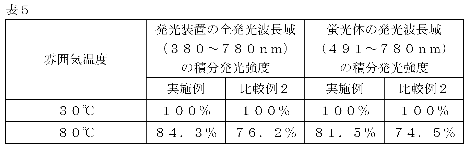
この表5から、発光装置の全発光波長域、及び蛍光体の発光波長域のいずれについても、実施例は比較例2よりも高い維持率を示しており、実施例は良好な温度特性を有することが分かる。
図14に、実施例の発光装置について、700mAの駆動電流における30℃条件下の発光スペクトル(実線)と80℃条件下の発光スペクトル(点線)を示す。
図15に、比較例2の発光装置について、700mAの駆動電流における30℃条件下の発光スペクトル(実線)と80℃条件下の発光スペクトル(点線)を示す。
図14及び図15から、30℃条件下から80℃条件下への温度上昇により、いずれの発光装置も発光スペクトルの発光強度が低下するが、実施例は比較例2に比べて蛍光領域が高く維持されていることが分かる。
以上、本発明の蛍光体を実施例に沿って説明したが、本発明はこれらの実施例に限られるものではなく、種々の変更、改良、組み合わせ、利用形態等が考えられることは言うまでもない。
本出願は、2008年2月18日出願の日本特許出願(特願2008-035461)に基づくものであり、その内容はここに参照として取り込まれる。
本発明の白色発光装置は、車両用灯具であって光源の機能色が白色系のもの、例えばヘッドランプ、フォグランプ、コーナーリングランプ、ライセンスプレートランプ、バックアップランプ、ルームランプ等に利用することができる。
また、本発明の白色発光装置は、白色光源とカラーフィルター等を組み合わせた車両用灯具であって機能色が白色系以外のもの、例えばテールランプ、ストップランプ、ターンシグナルランプ等に利用することもできる。
また、本発明の白色発光装置は、白色光源とカラーフィルター等を組み合わせた車両用灯具であって機能色が白色系以外のもの、例えばテールランプ、ストップランプ、ターンシグナルランプ等に利用することもできる。
Claims (9)
- 車両用灯具に用いられる白色発光装置であって、
370~480nmの波長域に発光スペクトルのピークを持つ半導体発光素子と、前記半導体発光素子の発する光により励起され可視光を発光する少なくとも2種以上の蛍光体を備え、
前記蛍光体は、SrxBaySi2O2N2:Eu2+の一般式で表され、前記一般式におけるyに対するxの比の値x/yが100/0~60/40の範囲内にある第一の蛍光体と、前記比の値x/yが45/55~5/95の範囲内にある第二の蛍光体とを備えることを特徴とする白色発光装置。 - 前記比の値x/yが100/0~70/30の範囲内にある第一の蛍光体と、前記比の値x/yが40/60~5/95の範囲内にある第二の蛍光体とを備えることを特徴とする請求項1~2のいずれかに記載の白色発光装置。
- 前記一般式のxが0.60<x<0.97、yが0≦y<0.35、x+yがx+y<0.97の範囲にある第一の蛍光体と、前記一般式のxが0.03<x<0.40、yが0.40<y<0.90、x+yがx+y<0.97の範囲にある第二の蛍光体とを備えることを特徴とする請求項1~2のいずれかに記載の白色発光装置。
- 前記第一の蛍光体の発光スペクトルのドミナント波長が550~565nmの波長域にあり、前記第二の蛍光体の発光スペクトルのドミナント波長が578~600nmの波長域にあることを特徴とする請求項1~3のいずれかに記載の白色発光装置。
- 前記第一の蛍光体の発光スペクトルのピーク波長が535~570nmの波長域にあり、前記第二の蛍光体の発光スペクトルのピーク波長が575~610nmの波長域にあることを特徴とする1~4のいずれかに記載の白色発光装置。
- 前記第一の蛍光体及び前記第二の蛍光体の合成スペクトルのドミナント波長が565~580nmの波長域にあり、半値幅が100nm以上であることを特徴とする請求項1~5のいずれかに記載の白色発光装置。
- 前記第一の蛍光体及び前記第二の蛍光体は、SrCO3、BaCO3、SiO2及びEu2O3の混合物を還元雰囲気中で1次焼成して作製したユーロピウム付活のオルソ珪酸塩を前駆体とし、この前駆体とSi3N4及びNH4Clの混合物を還元雰囲気中で2次焼成することで得られることを特徴とする請求項1~6のいずれかに記載の白色発光装置。
- 前記半導体発光素子のピーク波長が430nm~470nmの波長域にあるInGaN系LEDであることを特徴とする請求項1~7のいずれかに記載の白色発光装置。
- 請求項1~8のいずれかに記載の白色発光装置を光源とした車両用灯具。
Priority Applications (1)
| Application Number | Priority Date | Filing Date | Title |
|---|---|---|---|
| JP2009554353A JPWO2009104652A1 (ja) | 2008-02-18 | 2009-02-18 | 白色発光装置及びこれを用いた車両用灯具 |
Applications Claiming Priority (2)
| Application Number | Priority Date | Filing Date | Title |
|---|---|---|---|
| JP2008-035461 | 2008-02-18 | ||
| JP2008035461 | 2008-02-18 |
Publications (1)
| Publication Number | Publication Date |
|---|---|
| WO2009104652A1 true WO2009104652A1 (ja) | 2009-08-27 |
Family
ID=40985530
Family Applications (1)
| Application Number | Title | Priority Date | Filing Date |
|---|---|---|---|
| PCT/JP2009/052819 Ceased WO2009104652A1 (ja) | 2008-02-18 | 2009-02-18 | 白色発光装置及びこれを用いた車両用灯具 |
Country Status (2)
| Country | Link |
|---|---|
| JP (1) | JPWO2009104652A1 (ja) |
| WO (1) | WO2009104652A1 (ja) |
Cited By (3)
| Publication number | Priority date | Publication date | Assignee | Title |
|---|---|---|---|---|
| KR101264309B1 (ko) * | 2011-03-11 | 2013-05-22 | 한국세라믹기술원 | 산질화물 형광체 및 그 제조방법 |
| US8513872B2 (en) | 2010-08-05 | 2013-08-20 | Sharp Kabushiki Kaisha | Light emitting apparatus and method for manufacturing thereof |
| CN110970542A (zh) * | 2018-09-28 | 2020-04-07 | 日亚化学工业株式会社 | 发光装置和具备其的灯具 |
Citations (2)
| Publication number | Priority date | Publication date | Assignee | Title |
|---|---|---|---|---|
| JP2005281700A (ja) * | 2002-10-16 | 2005-10-13 | Nichia Chem Ind Ltd | オキシ窒化物蛍光体を用いた発光装置 |
| JP2007242717A (ja) * | 2006-03-06 | 2007-09-20 | Koito Mfg Co Ltd | 車両用灯具 |
-
2009
- 2009-02-18 WO PCT/JP2009/052819 patent/WO2009104652A1/ja not_active Ceased
- 2009-02-18 JP JP2009554353A patent/JPWO2009104652A1/ja active Pending
Patent Citations (2)
| Publication number | Priority date | Publication date | Assignee | Title |
|---|---|---|---|---|
| JP2005281700A (ja) * | 2002-10-16 | 2005-10-13 | Nichia Chem Ind Ltd | オキシ窒化物蛍光体を用いた発光装置 |
| JP2007242717A (ja) * | 2006-03-06 | 2007-09-20 | Koito Mfg Co Ltd | 車両用灯具 |
Non-Patent Citations (2)
| Title |
|---|
| "Extended Abstracts, 67th Autumn Meeting, The Japan Society of Applied Physics", 2006, article KAICHO MIYAMOTO ET AL.: "Sanchikkabutsu Aoiro Keikotai (Sr, Ba)Si2O2N2:Eu2+ no Hakko Tokusei", pages: 1305 * |
| BONG-GOO YUN ET AL.: "Luminescence Properties of (Sr1-uBau)Si2O2N2:Eu2+, Yellow or Orange Phosphors for White LEDs, Synthesized with (Sr1-uBau) SiO4: Eu2+ as a Precursor", JOURNAL OF THE ELECTROCHEMICAL SOCIETY, vol. 154, no. 10, 15 August 2007 (2007-08-15), pages J320 - J325 * |
Cited By (3)
| Publication number | Priority date | Publication date | Assignee | Title |
|---|---|---|---|---|
| US8513872B2 (en) | 2010-08-05 | 2013-08-20 | Sharp Kabushiki Kaisha | Light emitting apparatus and method for manufacturing thereof |
| KR101264309B1 (ko) * | 2011-03-11 | 2013-05-22 | 한국세라믹기술원 | 산질화물 형광체 및 그 제조방법 |
| CN110970542A (zh) * | 2018-09-28 | 2020-04-07 | 日亚化学工业株式会社 | 发光装置和具备其的灯具 |
Also Published As
| Publication number | Publication date |
|---|---|
| JPWO2009104652A1 (ja) | 2011-06-23 |
Similar Documents
| Publication | Publication Date | Title |
|---|---|---|
| CN101031630B (zh) | 荧光体和使用该荧光体的发光装置、以及图像显示装置和照明装置 | |
| US8754432B2 (en) | Light emitting device | |
| US20070090381A1 (en) | Semiconductor light emitting device | |
| WO2009104653A1 (ja) | 白色発光装置及びこれを用いた車両用灯具 | |
| KR20100097097A (ko) | 발광 장치, 그것을 이용한 차량용 등구, 및 헤드 램프 | |
| JP2003273409A (ja) | 赤色不足補償蛍光発光素子 | |
| JP5635268B2 (ja) | 白色発光装置及びこれを用いた車両用灯具 | |
| JP2009040918A (ja) | 蛍光体及びその製造方法、蛍光体含有組成物、発光装置、並びに画像表示装置及び照明装置 | |
| JP7454785B2 (ja) | 蛍光体およびそれを使用した発光装置 | |
| JP2009040944A (ja) | 蛍光体、蛍光体含有組成物、発光装置、照明装置、及び、画像表示装置 | |
| CN105793391B (zh) | 发光材料混合物、具有发光材料混合物的发光半导体器件和具有发光材料混合物的路灯 | |
| EP3916073B1 (en) | Light emitting device | |
| WO2009104652A1 (ja) | 白色発光装置及びこれを用いた車両用灯具 | |
| JP6083048B2 (ja) | 蛍光体及び発光装置 | |
| JP2013089769A (ja) | 発光モジュール | |
| WO2013118334A1 (ja) | 蛍光体及び発光装置 | |
| JP5919014B2 (ja) | 蛍光体及び発光装置 | |
| JP2013227527A (ja) | 蛍光体及びこれを用いた発光装置 | |
| JP7361314B2 (ja) | 蛍光体およびそれを使用した発光装置 | |
| JP7345141B2 (ja) | 蛍光体およびそれを使用した発光装置 | |
| JP2006332202A (ja) | 発光装置、発光装置の製造方法、及びそれを用いた照明装置、画像表示装置用バックライト並びに画像表示装置 | |
| JP5919015B2 (ja) | 蛍光体及び発光装置 | |
| WO2023145774A1 (ja) | 蛍光体、その製造方法、および、発光デバイス | |
| JP5901987B2 (ja) | 蛍光体及び発光装置 | |
| JP2012144685A (ja) | 蛍光体及び発光装置 |
Legal Events
| Date | Code | Title | Description |
|---|---|---|---|
| 121 | Ep: the epo has been informed by wipo that ep was designated in this application |
Ref document number: 09711531 Country of ref document: EP Kind code of ref document: A1 |
|
| WWE | Wipo information: entry into national phase |
Ref document number: 2009554353 Country of ref document: JP |
|
| NENP | Non-entry into the national phase |
Ref country code: DE |
|
| 122 | Ep: pct application non-entry in european phase |
Ref document number: 09711531 Country of ref document: EP Kind code of ref document: A1 |