WO2008015533A2 - Porous dielectric layers obtained from pore -forming precursors - Google Patents
Porous dielectric layers obtained from pore -forming precursors Download PDFInfo
- Publication number
- WO2008015533A2 WO2008015533A2 PCT/IB2007/002184 IB2007002184W WO2008015533A2 WO 2008015533 A2 WO2008015533 A2 WO 2008015533A2 IB 2007002184 W IB2007002184 W IB 2007002184W WO 2008015533 A2 WO2008015533 A2 WO 2008015533A2
- Authority
- WO
- WIPO (PCT)
- Prior art keywords
- volumes
- precursor
- matrix
- myrtenol
- jasmone
- Prior art date
- Legal status (The legal status is an assumption and is not a legal conclusion. Google has not performed a legal analysis and makes no representation as to the accuracy of the status listed.)
- Ceased
Links
- AUHZEENZYGFFBQ-UHFFFAOYSA-N Cc1cc(C)cc(C)c1 Chemical compound Cc1cc(C)cc(C)c1 AUHZEENZYGFFBQ-UHFFFAOYSA-N 0.000 description 1
Classifications
-
- C—CHEMISTRY; METALLURGY
- C23—COATING METALLIC MATERIAL; COATING MATERIAL WITH METALLIC MATERIAL; CHEMICAL SURFACE TREATMENT; DIFFUSION TREATMENT OF METALLIC MATERIAL; COATING BY VACUUM EVAPORATION, BY SPUTTERING, BY ION IMPLANTATION OR BY CHEMICAL VAPOUR DEPOSITION, IN GENERAL; INHIBITING CORROSION OF METALLIC MATERIAL OR INCRUSTATION IN GENERAL
- C23C—COATING METALLIC MATERIAL; COATING MATERIAL WITH METALLIC MATERIAL; SURFACE TREATMENT OF METALLIC MATERIAL BY DIFFUSION INTO THE SURFACE, BY CHEMICAL CONVERSION OR SUBSTITUTION; COATING BY VACUUM EVAPORATION, BY SPUTTERING, BY ION IMPLANTATION OR BY CHEMICAL VAPOUR DEPOSITION, IN GENERAL
- C23C16/00—Chemical coating by decomposition of gaseous compounds, without leaving reaction products of surface material in the coating, i.e. chemical vapour deposition [CVD] processes
- C23C16/22—Chemical coating by decomposition of gaseous compounds, without leaving reaction products of surface material in the coating, i.e. chemical vapour deposition [CVD] processes characterised by the deposition of inorganic material, other than metallic material
- C23C16/30—Deposition of compounds, mixtures or solid solutions, e.g. borides, carbides, nitrides
- C23C16/40—Oxides
- C23C16/401—Oxides containing silicon
-
- H—ELECTRICITY
- H10—SEMICONDUCTOR DEVICES; ELECTRIC SOLID-STATE DEVICES NOT OTHERWISE PROVIDED FOR
- H10P—GENERIC PROCESSES OR APPARATUS FOR THE MANUFACTURE OR TREATMENT OF DEVICES COVERED BY CLASS H10
- H10P14/00—Formation of materials, e.g. in the shape of layers or pillars
- H10P14/60—Formation of materials, e.g. in the shape of layers or pillars of insulating materials
- H10P14/63—Formation of materials, e.g. in the shape of layers or pillars of insulating materials characterised by the formation processes
- H10P14/6326—Deposition processes
- H10P14/6328—Deposition from the gas or vapour phase
- H10P14/6334—Deposition from the gas or vapour phase using decomposition or reaction of gaseous or vapour phase compounds, i.e. chemical vapour deposition
- H10P14/6336—Deposition from the gas or vapour phase using decomposition or reaction of gaseous or vapour phase compounds, i.e. chemical vapour deposition in the presence of a plasma [PECVD]
-
- H—ELECTRICITY
- H10—SEMICONDUCTOR DEVICES; ELECTRIC SOLID-STATE DEVICES NOT OTHERWISE PROVIDED FOR
- H10P—GENERIC PROCESSES OR APPARATUS FOR THE MANUFACTURE OR TREATMENT OF DEVICES COVERED BY CLASS H10
- H10P14/00—Formation of materials, e.g. in the shape of layers or pillars
- H10P14/60—Formation of materials, e.g. in the shape of layers or pillars of insulating materials
- H10P14/68—Organic materials, e.g. photoresists
- H10P14/683—Organic materials, e.g. photoresists carbon-based polymeric organic materials, e.g. polyimides, poly cyclobutene or PVC
-
- H—ELECTRICITY
- H10—SEMICONDUCTOR DEVICES; ELECTRIC SOLID-STATE DEVICES NOT OTHERWISE PROVIDED FOR
- H10P—GENERIC PROCESSES OR APPARATUS FOR THE MANUFACTURE OR TREATMENT OF DEVICES COVERED BY CLASS H10
- H10P14/00—Formation of materials, e.g. in the shape of layers or pillars
- H10P14/60—Formation of materials, e.g. in the shape of layers or pillars of insulating materials
- H10P14/66—Formation of materials, e.g. in the shape of layers or pillars of insulating materials characterised by the type of materials
- H10P14/665—Porous materials
-
- H—ELECTRICITY
- H10—SEMICONDUCTOR DEVICES; ELECTRIC SOLID-STATE DEVICES NOT OTHERWISE PROVIDED FOR
- H10P—GENERIC PROCESSES OR APPARATUS FOR THE MANUFACTURE OR TREATMENT OF DEVICES COVERED BY CLASS H10
- H10P14/00—Formation of materials, e.g. in the shape of layers or pillars
- H10P14/60—Formation of materials, e.g. in the shape of layers or pillars of insulating materials
- H10P14/69—Inorganic materials
- H10P14/692—Inorganic materials composed of oxides, glassy oxides or oxide-based glasses
- H10P14/6921—Inorganic materials composed of oxides, glassy oxides or oxide-based glasses containing silicon
- H10P14/6922—Inorganic materials composed of oxides, glassy oxides or oxide-based glasses containing silicon the material containing Si, O and at least one of H, N, C, F or other non-metal elements, e.g. SiOC, SiOC:H or SiONC
-
- Y—GENERAL TAGGING OF NEW TECHNOLOGICAL DEVELOPMENTS; GENERAL TAGGING OF CROSS-SECTIONAL TECHNOLOGIES SPANNING OVER SEVERAL SECTIONS OF THE IPC; TECHNICAL SUBJECTS COVERED BY FORMER USPC CROSS-REFERENCE ART COLLECTIONS [XRACs] AND DIGESTS
- Y10—TECHNICAL SUBJECTS COVERED BY FORMER USPC
- Y10T—TECHNICAL SUBJECTS COVERED BY FORMER US CLASSIFICATION
- Y10T428/00—Stock material or miscellaneous articles
- Y10T428/249921—Web or sheet containing structurally defined element or component
- Y10T428/249953—Composite having voids in a component [e.g., porous, cellular, etc.]
-
- Y—GENERAL TAGGING OF NEW TECHNOLOGICAL DEVELOPMENTS; GENERAL TAGGING OF CROSS-SECTIONAL TECHNOLOGIES SPANNING OVER SEVERAL SECTIONS OF THE IPC; TECHNICAL SUBJECTS COVERED BY FORMER USPC CROSS-REFERENCE ART COLLECTIONS [XRACs] AND DIGESTS
- Y10—TECHNICAL SUBJECTS COVERED BY FORMER USPC
- Y10T—TECHNICAL SUBJECTS COVERED BY FORMER US CLASSIFICATION
- Y10T428/00—Stock material or miscellaneous articles
- Y10T428/249921—Web or sheet containing structurally defined element or component
- Y10T428/249953—Composite having voids in a component [e.g., porous, cellular, etc.]
- Y10T428/249967—Inorganic matrix in void-containing component
- Y10T428/249969—Of silicon-containing material [e.g., glass, etc.]
Definitions
- the present invention relates to pore-forming precursors capable of generating volumes free of matter in a dielectric and also to the porous dielectric layers thus formed.
- interlayer dielectrics The insulating dielectric layers (known as "interlayer dielectrics") used to separate the metal interconnects between the various electrical circuits of an integrated circuit have to have increasingly low dielectric constants.
- ULK or ultra-low dielectric constant or ultra-low k porous materials.
- a particular treatment heating, exposure to ultraviolet radiation, electron bombardment
- the organic molecules and/or their thermal decomposition products which creates cavities free of solid matter in the "matrix” dielectric film (for example, an SiOCH film).
- the so-called “matrix” dielectric is described in detail in the patents or patent applications referenced above: it is generally formed from a material deposited using precursor molecules containing silicon, carbon, oxygen and hydrogen atoms, more particularly siloxanes such as TMCTS (1 ,3,5,7- tetramethylcyclotetrasiloxane) or OMCTS (octamethylcyclotetrasiloxane) or certain silane derivatives such as diethoxymethylsilane).
- siloxanes such as TMCTS (1 ,3,5,7- tetramethylcyclotetrasiloxane) or OMCTS (octamethylcyclotetrasiloxane) or certain silane derivatives such as diethoxymethylsilane).
- This step during which this porosity is created in the "matrix", conditions the final success of the production of these films and the mechanical quality of the layers mainly depends on the choice of the matrix molecule and pore-forming molecule combination.
- the hybrid material should preferably be both capable of releasing matter under the effect of a treatment, while keeping a stable framework during this release step, but also during the subsequent steps of manufacturing the semiconductor, especially during the steps of polishing the dielectric layers.
- the invention proposes to solve the problem posed by the selection of suitable pore-forming organic precursor molecules which, in combination with the "matrix" molecules, will make it possible to generate, on a substrate, a matrix precursor and organic precursor film that has a very low dielectric constant, while enabling the film to have good mechanical strength.
- the organic precursors according to the invention make it possible to solve the problem thus posed.
- each R possibly being independently chosen from H or linear or branched C 1 -C 5 alkyls.
- the porous layer of dielectric having a low dielectric constant k obtained from at least one matrix precursor and at least one organic precursor, is characterized in that it is composed of a plurality of first volumes comprising solid matter made of matrix precursor and/or matter derived, especially following a heat treatment, from a plurality of second volumes that do not comprise solid matter and of a plurality of third volumes, generally positioned between at least one first volume and at least one second volume and representing less than 1% of the total volume of the porous layer, these third volumes being formed from at least one fraction of organic precursor and/or of derived matter, which may or may not be linked to the matrix precursor, said organic precursor comprising at least one molecule chosen from the following molecules:
- each R possibly being independently chosen from H or linear or branched Ci-C 5 alkyls, the dielectric constant of said porous layer being less than or equal to 2.5;
- derived products is also understood to mean the products derived from these organic precursors and which, following the treatment undergone by the layer (heat treatment, ion bombardment, etc.) are converted alone, or in contact with the matrix molecules, to generate non-gaseous products that are not capable of being removed by diffusion through the layer as the gaseous products derived from the decomposition of the organic precursors generally do).
- This layer may be obtained by deposition on a substrate of the 300 mm wafer type in a "PECVD" type reactor by injection of the two precursors using a carrier gas such as He, for example, then heat treatment at a temperature of around 400 0 C.
- a carrier gas such as He
- the molecules mentioned above are commercially available and relatively inexpensive, have a moderate toxicity, good volatility, several reactive chemical functional groups (for example, unsaturation, ring, carbonyl functional group), sufficient chemical stability so that the packaging, transport and/or storage and also the use do not affect the molecule, and do not require the addition of a stabilizer.
- reactive chemical functional groups for example, unsaturation, ring, carbonyl functional group
- the assembly was then subjected, in a manner known per se, to a heat treatment step, at a temperature of the order of around 35O 0 C to 450 0 C, for a duration generally of a few tens of minutes, which may or may not be followed by an ion bombardment step, then optionally by a treatment in a moist atmosphere and then drying, as described, for example, in US-A-2005/ 0227502.
- the organic precursor is decomposed under the effect of the heat, giving rise to cavities 4 that are free of matter, with however some volumes 5 in which it is possible to identify residual organic matter that has not been completely decomposed, these volumes 5 being located between the volume 3 of matrix precursor and the volumes 4 free of matter.
- the matrix precursor volume 3 (also called the first volume in the present application) is generally formed from a single volume having continuity (giving the layer the desired mechanical strength) in which a plurality of second and third volumes 4 and 5 are located.
- These porous layers having a low dielectric constant that is usually less than 2.5 can be used in manufacturing integrated circuits, flat screens, memory (especially so-called "random access memory") and any similar applications in which a dielectric layer with low dielectric constant is used to insulate two electrical components (dielectric interconnect layers).
- BEOL back end of the line
Landscapes
- Chemical & Material Sciences (AREA)
- Inorganic Chemistry (AREA)
- General Chemical & Material Sciences (AREA)
- Chemical Kinetics & Catalysis (AREA)
- Engineering & Computer Science (AREA)
- Materials Engineering (AREA)
- Mechanical Engineering (AREA)
- Metallurgy (AREA)
- Organic Chemistry (AREA)
- Internal Circuitry In Semiconductor Integrated Circuit Devices (AREA)
- Formation Of Insulating Films (AREA)
- Manufacture Of Porous Articles, And Recovery And Treatment Of Waste Products (AREA)
Abstract
The invention relates to porous dielectric layers obtained from pore -forming precursors and from matrix precursors. According to the invention, the pore- forming precursors used are chosen from molecules of myrtenol, ethyl chrysanthemumate, jasmone, trimethylbenzene, their positional isomers and their substituted or hydrogenated derivatives. The dielectric constant of the layer obtained is less than or equal to 2.5, starting from matrix precursors having a dielectric constant of less than or equal 4.
Description
NOVEL PORE-FORMING PRECURSORS AND POROUS DIELECTRIC LAYERS OBTAINED THEREFROM
The present invention relates to pore-forming precursors capable of generating volumes free of matter in a dielectric and also to the porous dielectric layers thus formed.
The insulating dielectric layers (known as "interlayer dielectrics") used to separate the metal interconnects between the various electrical circuits of an integrated circuit have to have increasingly low dielectric constants.
For this, it is possible to create porosity in the dielectric itself (that is to say create microcavities free of solid matter) and thus to take advantage of the dielectric constant of air, which is equal to 1.
These are then referred to as ULK (or ultra-low dielectric constant or ultra-low k) porous materials.
To produce such porous layers, conventional low dielectric constant precursors, also known as "matrix" precurors are combined, during the deposition, with organic precursors that are known as pore-forming organic molecules and which have the property of enabling the creation of pores in the "matrix" precursor.
The hybrid film that is obtained, for example by "PECVD" type deposition on a semiconductor substrate, then undergoes a particular treatment (heating, exposure to ultraviolet radiation, electron bombardment) which results in the release of a certain number of chemical molecules from the film (the organic molecules and/or their thermal decomposition products), which creates cavities free of solid matter in the "matrix" dielectric film (for example, an SiOCH film). For further details on the formation of these films reference may be made, for example, to Patent Application WO 2005/112095, or to Patent Application US-A-2002/037442 or to Patent US-A-6312793.
The objective of such films is to create porosity in the "matrix" dielectric, without the structure of the film collapsing, that is to say to obtain a film that still has sufficient mechanical properties;
(the so-called "matrix" dielectric is described in detail in the patents or patent applications referenced above: it is generally formed from a material deposited using precursor molecules containing silicon, carbon, oxygen and hydrogen atoms, more particularly siloxanes such as TMCTS (1 ,3,5,7- tetramethylcyclotetrasiloxane) or OMCTS (octamethylcyclotetrasiloxane) or certain silane derivatives such as diethoxymethylsilane).
This step, during which this porosity is created in the "matrix", conditions the final success of the production of these films and the mechanical quality of the layers mainly depends on the choice of the matrix molecule and pore-forming molecule combination.
The hybrid material should preferably be both capable of releasing matter under the effect of a treatment, while keeping a stable framework during this release step, but also during the subsequent steps of manufacturing the semiconductor, especially during the steps of polishing the dielectric layers.
The invention proposes to solve the problem posed by the selection of suitable pore-forming organic precursor molecules which, in combination with the "matrix" molecules, will make it possible to generate, on a substrate, a matrix precursor and organic precursor film that has a very low dielectric constant, while enabling the film to have good mechanical strength.
The organic precursors according to the invention make it possible to solve the problem thus posed.
They are characterized in that they comprise at least one molecule chosen from the following molecules:
2,2-dimethyl-3-(2-methylpropenyl)cyclopropanecarboxylic acid ethyl ester, (better known under the name ethyl chrysanthemumate), of formula:

Ethyl Chrysanthemumate
3-methyl-2-(2-pentenyl)-2-cyclopenten-1-one, or jasmone, of formula:

Jasmone
6,6-dimethyl-2-(hydroxymethyl)bicyclo[3.1.1]hept-2-ene, or myrtenol, of formula:

Myrtenol
1 , 3, 5-tri methyl benzene, or mesytilene, of formula:

and also their positional isomers and/or their derivatives in which at least one of the terminal methyls and/or hydrogens is replaced by an R group, each R
possibly being independently chosen from H or linear or branched C1-C5 alkyls.
According to another aspect of the invention, the porous layer of dielectric having a low dielectric constant k, obtained from at least one matrix precursor and at least one organic precursor, is characterized in that it is composed of a plurality of first volumes comprising solid matter made of matrix precursor and/or matter derived, especially following a heat treatment, from a plurality of second volumes that do not comprise solid matter and of a plurality of third volumes, generally positioned between at least one first volume and at least one second volume and representing less than 1% of the total volume of the porous layer, these third volumes being formed from at least one fraction of organic precursor and/or of derived matter, which may or may not be linked to the matrix precursor, said organic precursor comprising at least one molecule chosen from the following molecules:
2,2-dimethyl-3-(2-methylpropenyl)cyclopropanecarboxylic acid ethyl ester, (better known under the name ethyl chrysanthemumate);

Ethyl Chrysanthemumate
3-methyl-2-(2-pentenyl)-2-cyclopenten-1 -one, or jasmone;
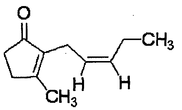
Jasmone
6,6-dimethyl-2-(hydroxymethyl)bicyclo[3.1.1]hept-2-ene, or myrtenol;

Myrtenol
1 ,3,5-trimethylbenzene, or mesytilene;

and also their positional isomers and/or their derivatives in which at least one of the terminal methyls and/or hydrogens is replaced by an R group, each R possibly being independently chosen from H or linear or branched Ci-C5 alkyls, the dielectric constant of said porous layer being less than or equal to 2.5;
(the term "derived products" is also understood to mean the products derived from these organic precursors and which, following the treatment undergone by the layer (heat treatment, ion bombardment, etc.) are converted alone, or in contact with the matrix molecules, to generate non-gaseous products that are not capable of being removed by diffusion through the layer as the gaseous products derived from the decomposition of the organic precursors generally do).
This layer may be obtained by deposition on a substrate of the 300 mm wafer type in a "PECVD" type reactor by injection of the two precursors using a carrier gas such as He, for example, then heat treatment at a temperature of around 4000C.
The advantages of the pore-forming precursors according to the invention are the following:
The molecules mentioned above are commercially available and relatively inexpensive, have a moderate toxicity, good volatility, several reactive chemical functional groups (for example, unsaturation, ring, carbonyl functional group), sufficient chemical stability so that the packaging, transport and/or storage and also the use do not affect the molecule, and do not require the addition of a stabilizer.
The single figure schematically shows the porous layer obtained according to the invention:
Deposited by the so-called PECVD process, on a substrate 1 , was a layer 2 initially consisting of a mixture of a "matrix" precursor 3 and an organic precursor, deposited from their gaseous phases (as, for example, described in the aforementioned patent and patent applications).
The assembly was then subjected, in a manner known per se, to a heat treatment step, at a temperature of the order of around 35O0C to 4500C, for a duration generally of a few tens of minutes, which may or may not be followed by an ion bombardment step, then optionally by a treatment in a moist atmosphere and then drying, as described, for example, in US-A-2005/ 0227502.
During the heat treatment, the organic precursor is decomposed under the effect of the heat, giving rise to cavities 4 that are free of matter, with however some volumes 5 in which it is possible to identify residual organic matter that has not been completely decomposed, these volumes 5 being located between the volume 3 of matrix precursor and the volumes 4 free of matter.
These volumes 5 will preferably always represent less than 1 vol% of the layer after heat (or other) treatment, more preferably less than a few hundred ppm. The matrix precursor volume 3 (also called the first volume in the present application) is generally formed from a single volume having continuity (giving the layer the desired mechanical strength) in which a plurality of second and third volumes 4 and 5 are located.
These porous layers having a low dielectric constant that is usually less than 2.5, can be used in manufacturing integrated circuits, flat screens, memory (especially so-called "random access memory") and any similar applications in which a dielectric layer with low dielectric constant is used to insulate two electrical components (dielectric interconnect layers).
They will be more particularly used in the interconnect circuits of the various components of an integrated circuit, called BEOL ("back end of the line") components.
Claims
1. Porous layer of dielectric having a low dielectric constant k obtained from at least one matrix precursor and at least one organic precursor, characterized in that it is composed of a plurality of first volumes (3) comprising solid matter made of matrix precursor and/or matter derived, especially following a heat treatment, from a plurality of second volumes (4) that do not comprise solid matter and of a plurality of third volumes (5), generally positioned between at least one first volume (3) and at least one second volume (4) and representing less than 1% of the total volume of the porous layer (2), these third volumes being formed from at least one fraction of organic precursor and/or of derived matter, which may or may not be linked to the matrix precursor, said organic precursor comprising at least one molecule chosen from the following molecules:
2,2-dimethyl-3-(2-methylpropenyl)cyclopropanecarboxylic acid ethyl ester, (better known under the name ethyl chrysanthemumate);

Ethyl Chrysanthemumate
3-methyl-2-(2-pentenyl)-2-cyclopenten-1 -one, or jasmone;

Jasmone
6,6-dimethyl-2-(hydroxymethyl)bicyclo[3.1.1]hept-2-ene, or myrtenol; 
Myrtenol
1 ,3,5-trimethylbenzene, or mesytilene;

1 ,3,5-Trimethylbenzene
and also their positional isomers and/or their derivatives in which at least one of the terminal methyls and/or hydrogens is replaced by an R group, each R possibly being independently chosen from H or linear or branched CrC5 alkyls, the dielectric constant of said porous layer (2) being less than or equal to 2.5.
2. Use of pore-forming precursors capable of generating volumes free of solid matter in a dielectric of the "matrix" precursor type, characterized in that it comprises at least one molecule chosen from the following molecules:
2,2-dimethyl-3-(2-methylpropenyl)cyclopropanecarboxylic acid ethyl ester, (better known under the name ethyl chrysanthemumate);

Ethyl Chrysanthemumate 3-methyl-2-(2-pentenyl)-2-cyclopenten-1 -one, or jasmone;

Jasmone
6,6-dimethyl-2-(hydroxymethyl)bicyclo[3.1.1]hept-2-ene, or myrtenol;

Myrtenol
1 ,3,5-trimethylbenzene, or mesytilene;

1 ,3,5-Trimethylbenzene
and also their positional isomers and/or their derivatives in which at least one of the terminal methyls and/or hydrogens is replaced by an R group, each R possibly being independently chosen from H or linear or branched CrC5 alkyls,
for producing electrically insulating layers, especially in integrated circuits, more particularly for producing dielectric interconnect layers.
Priority Applications (1)
| Application Number | Priority Date | Filing Date | Title |
|---|---|---|---|
| US12/375,207 US8398885B2 (en) | 2006-08-01 | 2007-07-30 | Pore-forming precursors and porous dielectric layers obtained therefrom |
Applications Claiming Priority (2)
| Application Number | Priority Date | Filing Date | Title |
|---|---|---|---|
| FR0653228A FR2904728B1 (en) | 2006-08-01 | 2006-08-01 | NOVEL POROGENOUS PRECURSORS AND POROUS DIELECTRIC LAYERS OBTAINED THEREFROM |
| FR0653228 | 2006-08-01 |
Publications (2)
| Publication Number | Publication Date |
|---|---|
| WO2008015533A2 true WO2008015533A2 (en) | 2008-02-07 |
| WO2008015533A3 WO2008015533A3 (en) | 2008-07-03 |
Family
ID=37951586
Family Applications (1)
| Application Number | Title | Priority Date | Filing Date |
|---|---|---|---|
| PCT/IB2007/002184 Ceased WO2008015533A2 (en) | 2006-08-01 | 2007-07-30 | Porous dielectric layers obtained from pore -forming precursors |
Country Status (3)
| Country | Link |
|---|---|
| US (1) | US8398885B2 (en) |
| FR (1) | FR2904728B1 (en) |
| WO (1) | WO2008015533A2 (en) |
Cited By (1)
| Publication number | Priority date | Publication date | Assignee | Title |
|---|---|---|---|---|
| EP2339049A1 (en) | 2009-12-23 | 2011-06-29 | Air Products and Chemicals, Inc. | Precursors for providing materials with low dielectric constant and superior integration attributes |
Family Cites Families (4)
| Publication number | Priority date | Publication date | Assignee | Title |
|---|---|---|---|---|
| FR2267296A1 (en) | 1974-04-12 | 1975-11-07 | Anvar | Myrtenol synthesis - by isomerisation of beta-pinene epoxide |
| US6312793B1 (en) * | 1999-05-26 | 2001-11-06 | International Business Machines Corporation | Multiphase low dielectric constant material |
| US7049247B2 (en) | 2004-05-03 | 2006-05-23 | International Business Machines Corporation | Method for fabricating an ultralow dielectric constant material as an intralevel or interlevel dielectric in a semiconductor device and electronic device made |
| US7332445B2 (en) * | 2004-09-28 | 2008-02-19 | Air Products And Chemicals, Inc. | Porous low dielectric constant compositions and methods for making and using same |
-
2006
- 2006-08-01 FR FR0653228A patent/FR2904728B1/en not_active Expired - Fee Related
-
2007
- 2007-07-30 US US12/375,207 patent/US8398885B2/en not_active Expired - Fee Related
- 2007-07-30 WO PCT/IB2007/002184 patent/WO2008015533A2/en not_active Ceased
Cited By (3)
| Publication number | Priority date | Publication date | Assignee | Title |
|---|---|---|---|---|
| EP2339049A1 (en) | 2009-12-23 | 2011-06-29 | Air Products and Chemicals, Inc. | Precursors for providing materials with low dielectric constant and superior integration attributes |
| US8753986B2 (en) | 2009-12-23 | 2014-06-17 | Air Products And Chemicals, Inc. | Low k precursors providing superior integration attributes |
| US9018107B2 (en) | 2009-12-23 | 2015-04-28 | Air Products And Chemicals, Inc. | Low K precursors providing superior integration attributes |
Also Published As
| Publication number | Publication date |
|---|---|
| FR2904728A1 (en) | 2008-02-08 |
| US8398885B2 (en) | 2013-03-19 |
| FR2904728B1 (en) | 2008-11-21 |
| WO2008015533A3 (en) | 2008-07-03 |
| US20090321679A1 (en) | 2009-12-31 |
Similar Documents
| Publication | Publication Date | Title |
|---|---|---|
| US9293361B2 (en) | Materials and methods of forming controlled void | |
| JP3930840B2 (en) | Low-κ dielectric inorganic / organic hybrid film | |
| JP4874614B2 (en) | Porous low dielectric constant compositions and methods for making and using the same | |
| TWI613724B (en) | Method for forming SiOCH film by annealing with organic amine decane | |
| CN105177524B (en) | Alkyl-alkoxy silicon heterocyclic compound and method of depositing thin film using same | |
| JP2007531325A (en) | Multi-step curing of low dielectric constant nanoporous membranes | |
| TW201142945A (en) | Ultra low dielectric materials using hybrid precursors containing silicon with organic functional groups by plasma-enhanced chemical vapor deposition | |
| TWI676632B (en) | Alkoxysilacyclic or acyloxysilacyclic compounds and methods for depositing films using same | |
| JP4960439B2 (en) | Novel pore-forming precursor composition and porous dielectric layer obtained therefrom | |
| JP2010153824A (en) | Method of manufacturing porous insulating film, method of manufacturing semiconductor device, and semiconductor device | |
| US8398885B2 (en) | Pore-forming precursors and porous dielectric layers obtained therefrom | |
| US9449810B2 (en) | Advanced ultra low k SiCOH dielectrics prepared by built-in engineered pore size and bonding structured with cyclic organosilicon precursors | |
| KR101367141B1 (en) | Organometallic Precursor, Method of Forming a Thin Film using the Organometallic Precursor and Method of Manufacturing a Metal Wiring | |
| KR20190014617A (en) | Method of forming an ultra-low-k layer and the layer | |
| JPWO2005124846A1 (en) | Organic siloxane film, semiconductor device using the same, flat display device, and raw material liquid | |
| WO2011065221A1 (en) | Ruthenium-film forming material and ruthenium-film forming method | |
| FR2899379A1 (en) | NOVEL POROGENOUS PRECURSORS AND POROUS DIELECTRIC LAYERS OBTAINED THEREFROM | |
| FR2905517A1 (en) | New precursor mixture for formation of specific low dielectric porous film on substrate comprises film matrix precursor, and either keto compound or e.g. 1-methyl-4-(1-methylethyl)-7-oxabicyclo(2.2.1)heptane as pore-forming compound | |
| KR100856953B1 (en) | Organic siloxane film, semiconductor device using the same, and flat display device and raw material liquid | |
| KR20260043891A (en) | Low Dielectric Constant Film Forming Composition, the Low Dielectric Constant Film, and Method for Manufacturing the Same | |
| CN119008586A (en) | Semiconductor element with porous layer | |
| TW201937514A (en) | Manufacturing method of insulator film and insulator film making apparatus | |
| TW201833368A (en) | Methods of forming a dielectric layer and methods of fabricating a semiconductor device |
Legal Events
| Date | Code | Title | Description |
|---|---|---|---|
| 121 | Ep: the epo has been informed by wipo that ep was designated in this application |
Ref document number: 07804674 Country of ref document: EP Kind code of ref document: A2 |
|
| NENP | Non-entry into the national phase |
Ref country code: DE |
|
| NENP | Non-entry into the national phase |
Ref country code: RU |
|
| 122 | Ep: pct application non-entry in european phase |
Ref document number: 07804674 Country of ref document: EP Kind code of ref document: A2 |
|
| WWE | Wipo information: entry into national phase |
Ref document number: 12375207 Country of ref document: US |