WO2007018183A1 - Positive electrode collector for lead acid storage battery and method for producing same - Google Patents
Positive electrode collector for lead acid storage battery and method for producing same Download PDFInfo
- Publication number
- WO2007018183A1 WO2007018183A1 PCT/JP2006/315605 JP2006315605W WO2007018183A1 WO 2007018183 A1 WO2007018183 A1 WO 2007018183A1 JP 2006315605 W JP2006315605 W JP 2006315605W WO 2007018183 A1 WO2007018183 A1 WO 2007018183A1
- Authority
- WO
- WIPO (PCT)
- Prior art keywords
- current collector
- titanium
- positive electrode
- electrode current
- lead
- Prior art date
Links
Classifications
-
- H—ELECTRICITY
- H01—ELECTRIC ELEMENTS
- H01M—PROCESSES OR MEANS, e.g. BATTERIES, FOR THE DIRECT CONVERSION OF CHEMICAL ENERGY INTO ELECTRICAL ENERGY
- H01M4/00—Electrodes
- H01M4/02—Electrodes composed of, or comprising, active material
- H01M4/64—Carriers or collectors
- H01M4/66—Selection of materials
- H01M4/661—Metal or alloys, e.g. alloy coatings
-
- H—ELECTRICITY
- H01—ELECTRIC ELEMENTS
- H01M—PROCESSES OR MEANS, e.g. BATTERIES, FOR THE DIRECT CONVERSION OF CHEMICAL ENERGY INTO ELECTRICAL ENERGY
- H01M10/00—Secondary cells; Manufacture thereof
- H01M10/06—Lead-acid accumulators
-
- H—ELECTRICITY
- H01—ELECTRIC ELEMENTS
- H01M—PROCESSES OR MEANS, e.g. BATTERIES, FOR THE DIRECT CONVERSION OF CHEMICAL ENERGY INTO ELECTRICAL ENERGY
- H01M4/00—Electrodes
- H01M4/02—Electrodes composed of, or comprising, active material
- H01M4/64—Carriers or collectors
- H01M4/66—Selection of materials
- H01M4/664—Ceramic materials
-
- H—ELECTRICITY
- H01—ELECTRIC ELEMENTS
- H01M—PROCESSES OR MEANS, e.g. BATTERIES, FOR THE DIRECT CONVERSION OF CHEMICAL ENERGY INTO ELECTRICAL ENERGY
- H01M4/00—Electrodes
- H01M4/02—Electrodes composed of, or comprising, active material
- H01M4/64—Carriers or collectors
- H01M4/66—Selection of materials
- H01M4/665—Composites
- H01M4/667—Composites in the form of layers, e.g. coatings
-
- H—ELECTRICITY
- H01—ELECTRIC ELEMENTS
- H01M—PROCESSES OR MEANS, e.g. BATTERIES, FOR THE DIRECT CONVERSION OF CHEMICAL ENERGY INTO ELECTRICAL ENERGY
- H01M4/00—Electrodes
- H01M4/02—Electrodes composed of, or comprising, active material
- H01M4/64—Carriers or collectors
- H01M4/66—Selection of materials
- H01M4/68—Selection of materials for use in lead-acid accumulators
-
- H—ELECTRICITY
- H01—ELECTRIC ELEMENTS
- H01M—PROCESSES OR MEANS, e.g. BATTERIES, FOR THE DIRECT CONVERSION OF CHEMICAL ENERGY INTO ELECTRICAL ENERGY
- H01M4/00—Electrodes
- H01M4/02—Electrodes composed of, or comprising, active material
- H01M2004/026—Electrodes composed of, or comprising, active material characterised by the polarity
- H01M2004/028—Positive electrodes
-
- Y—GENERAL TAGGING OF NEW TECHNOLOGICAL DEVELOPMENTS; GENERAL TAGGING OF CROSS-SECTIONAL TECHNOLOGIES SPANNING OVER SEVERAL SECTIONS OF THE IPC; TECHNICAL SUBJECTS COVERED BY FORMER USPC CROSS-REFERENCE ART COLLECTIONS [XRACs] AND DIGESTS
- Y02—TECHNOLOGIES OR APPLICATIONS FOR MITIGATION OR ADAPTATION AGAINST CLIMATE CHANGE
- Y02E—REDUCTION OF GREENHOUSE GAS [GHG] EMISSIONS, RELATED TO ENERGY GENERATION, TRANSMISSION OR DISTRIBUTION
- Y02E60/00—Enabling technologies; Technologies with a potential or indirect contribution to GHG emissions mitigation
- Y02E60/10—Energy storage using batteries
-
- Y—GENERAL TAGGING OF NEW TECHNOLOGICAL DEVELOPMENTS; GENERAL TAGGING OF CROSS-SECTIONAL TECHNOLOGIES SPANNING OVER SEVERAL SECTIONS OF THE IPC; TECHNICAL SUBJECTS COVERED BY FORMER USPC CROSS-REFERENCE ART COLLECTIONS [XRACs] AND DIGESTS
- Y02—TECHNOLOGIES OR APPLICATIONS FOR MITIGATION OR ADAPTATION AGAINST CLIMATE CHANGE
- Y02P—CLIMATE CHANGE MITIGATION TECHNOLOGIES IN THE PRODUCTION OR PROCESSING OF GOODS
- Y02P70/00—Climate change mitigation technologies in the production process for final industrial or consumer products
- Y02P70/50—Manufacturing or production processes characterised by the final manufactured product
Definitions
- the present invention relates to a positive electrode current collector in which a conductive ceramic layer is formed on the surface of a current collector base material of titanium or a titanium alloy, and a method for manufacturing the same.
- a positive electrode current collector cannot be produced only with these conductive ceramic materials. This is because, 'although it is less cm, generally it (volume resistivity 10_ 6 ⁇ : ⁇ _5 ⁇ metals' such volume resistivity of the conductive ceramic 10 Omega cm or less) because compared if too large the is there.
- Non-Patent Documents 1 and 2 there is a proposal to form a positive electrode current collector for a lead storage battery by forming a conductive ceramic layer on the surface of a current collector base material of titanium or a titanium alloy (for example, Non-Patent Documents 1 and 2). These positive electrode current collectors are made of SnO (Sb doped), PtO, IrO, RuO, etc. on the surface of titanium.
- a 2 x 2 2 conductive ceramic is coated, and the surface is further coated with j8-PbO.
- the surface of the current collector base material of titanium or titanium alloy is coated with conductive ceramics having PtO force, and further coated with ⁇ -PbO and
- a lead dioxide electrode used as a solution DSA electrode has also been proposed (for example, see Patent Document 1).
- titanium having a conductive ceramic layer on its surface is used for a positive electrode current collector
- the conductivity of titanium is sufficiently higher than that of conductive ceramics.
- the conductivity of the positive electrode current collector is ensured.
- Titanium has high corrosion resistance Therefore, it is inherently difficult to dissolve in dilute sulfuric acid, which is the electrolyte for lead-acid batteries.
- a conductive ceramic layer is provided, dissolution of titanium will not be a problem.
- the melting point of titanium is high, it can withstand high temperatures of around 500 ° C in the process of providing a conductive ceramic layer.
- titanium has the property of being passivated, so that passivation of titanium is prevented by covering titanium with a conductive ceramic layer, so that passivation of titanium does not become a problem. Furthermore, since titanium is less expensive than conductive ceramics, material costs can be reduced.
- Non-Patent Document 1 Journal of the Electrochemical Society, Vol. 47 (668) The Electrochemical Society of Japan 1979
- Non-Patent Document 2 Journal of the Electrochemical Society, Vol. 48 (384) The Electrochemical Society of Japan 1980 Patent Document 1: JP-A 63-57791
- the cause of the above problem was a titanium oxide titanium coating between the current collector base material of titanium or titanium alloy and the conductive ceramic layer. I got it. That is, since there is titanium oxide having low conductivity between the current collector base material of titanium or titanium alloy and the conductive ceramic layer, the resistance of the positive electrode current collector is increased, which leads to the internal resistance of the lead-acid battery. It was getting bigger. It should be noted that this titanium oxide-titanium coating film is a titanium or titanium alloy current collector base material when firing is performed in such a manner that a conductive ceramic layer is provided on the surface of the titanium or titanium alloy current collector base material. It is thought that the surface layer part of this is generated by being oxidized.
- the present invention includes a current collector base material of titanium or a titanium alloy, a titanium oxide film provided on the surface of the current collector base material, and a conductive property provided on the surface of the film.
- a positive electrode current collector for a lead storage battery comprising a ceramic layer, wherein the thickness of the coating is 0.09 / zm or less.
- the titanium oxide film formed between the current collector substrate and the conductive ceramic layer is sufficiently thin. Therefore, the electrical resistance is reduced. Therefore, when a lead storage battery is manufactured using this positive electrode current collector, the high rate discharge performance of the lead storage battery is excellent.
- titanium oxide the stoichiometric ratio of titanium to oxygen is not always 1: 2. Therefore, in the present application, titanium oxide which is a component of the coating is represented as TiO. In this case, X is greater than 0 and less than or equal to 2.
- the thickness of the titanium oxide coating is determined by the Marcus high-frequency glow discharge luminescent surface analysis
- the conductive ceramic is a ceramic obtained by firing a metal compound such as a metal oxide or a metal silicide at a high temperature, and has a volume resistivity of 10 ⁇ 'cm or less.
- a metal compound such as a metal oxide or a metal silicide
- a volume resistivity 10 ⁇ 'cm or less.
- only one layer may be strong, or another layer such as ⁇ -PbO and
- the present invention relates to a method for producing a positive electrode current collector for a lead storage battery, the method comprising first annealing a current collector base material of titanium or a titanium alloy in a vacuum or in an inert atmosphere. And a second step of forming a conductive ceramic layer on the surface of the current collector base material that has undergone the first step.
- a positive electrode current collector for a lead storage battery having a coating thickness of 0.09 m or less. That is, current collector base material of titanium or titanium alloy Before the conductive ceramic layer is formed, the current collector base material of titanium or titanium alloy is annealed in a vacuum or in an inert atmosphere. For this reason, the recrystallization associated with annealing removes the crystal distortion of titanium or the titanium alloy and increases the crystallinity of the titanium or the titanium alloy.
- a vacuum refers to a vacuum in which a titanium or titanium alloy film is hardly formed on titanium or a titanium alloy during annealing. Therefore, although the vacuum here is preferably a high vacuum, it is not always necessary. In the examples of the present application, a low vacuum of 1 ⁇ 10_4 Pa was used as described later.
- An inert atmosphere means an atmosphere filled with a gas or an atmosphere in which such a gas is sufficiently circulated without reacting with titanium or a titanium alloy to form an acid film.
- the annealing temperature may be any temperature that can remove the crystal distortion of the current collector base material, and thus the temperature is not limited. Further, in the annealing step, a process of changing the annealing temperature with time may be performed. In the embodiment of the present application, examples of annealing after 700 hours at 700 ° C. are mainly shown.
- the second step includes a firing step. That is, the second step of forming the conductive ceramic layer includes a step of firing the current collector base material such as a dip coating method or a spray pyrolysis method. Details of these dip coating methods or spray pyrolysis methods will be described later.
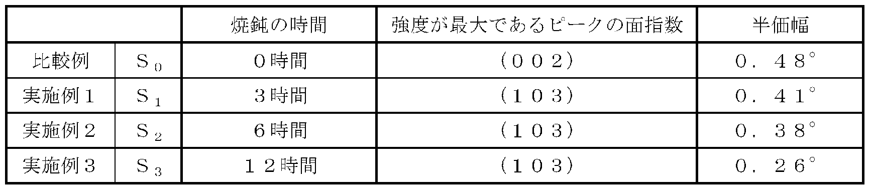
- the half width of the peak having the maximum intensity in the XRD pattern of the titanium or the titanium alloy is set to 0. It is characterized by being 38 ° or less. Further, in the manufacturing method as described above, when the four peaks are selected in descending order of the intensity in the XRD pattern of the titanium or the titanium alloy by the first step, the total value of the intensity of the four peaks The It is characterized by being 85% or more of the total intensity of all peaks.
- the surface of the current collector substrate has sufficiently high crystallinity, and crystal distortion is reliably removed. Therefore, even when the current collector substrate is heated at a high temperature to form a conductive ceramic layer, it is difficult to form a titanium oxide film. And the electrical resistance between the current collector substrate and the conductive ceramic layer is reduced.
- all peaks means that when the current collector base material is titanium, the (100) plane, (002) plane, (101) of titanium It is defined as a diffraction peak attributed to the plane, (102) plane, (110) plane, (103) plane, (200) plane, (112) plane, and (201) plane.
- These are diffraction peaks that appear when scanning 2 ⁇ up to 80 ° at 20 ° in XRD measurement.
- the current collector base material is a titanium alloy
- the XRD measurement shows a diffraction peak that appears when 2 ⁇ is scanned up to 80 ° at 20 ° force, and the intensity with respect to the peak having the maximum intensity. Those with a ratio of 1% or more (including peaks with maximum intensity).
- the present invention relates to a positive electrode current collector for a lead storage battery comprising a current collector base material of titanium or a titanium alloy and a conductive ceramic layer, wherein the conductive ceramic layer includes the current collector base.
- a positive electrode current collector for a lead storage battery comprising a current collector base material of titanium or a titanium alloy and a conductive ceramic layer, wherein the conductive ceramic layer includes the current collector base.
- the half width of the peak having the maximum intensity among the peaks of the titanium or titanium alloy is 0.38 ° or less. .
- the present invention relates to a positive electrode current collector for a lead storage battery comprising a current collector base material of titanium or a titanium alloy and a conductive ceramic layer, wherein the conductive ceramic layer is the current collector base material.
- the total value of the intensity of the four peaks when four peaks are selected in descending order of the intensity of the titanium or titanium alloy peaks. It is characterized by being greater than 85% of the total peak intensity.
- a thick titanium oxide film is not formed between the current collector base material and the conductive ceramic layer in the positive electrode current collector. Therefore, the electrical resistance between the current collector substrate and the conductive ceramic layer is reduced.
- the present invention is characterized in that a lead storage battery is provided with the positive electrode current collector as described above.
- the present invention also relates to a lead storage device including the positive current collector as described above in an uninterruptible power supply. It is equipped with a pond.
- the high-rate discharge performance of the lead storage battery and the uninterruptible power supply is excellent.
- the present invention provides a method for producing a lead-acid battery including a positive electrode current collector, wherein the method for producing the positive electrode current collector is a production method as described above. To do.
- the present invention relates to a method for manufacturing an uninterruptible power supply equipped with a lead-acid battery equipped with a positive electrode current collector, and that the method for manufacturing the positive electrode current collector is a method as described above.
- the high rate discharge performance of the lead storage battery manufactured by these inventions is excellent. Moreover, the high rate discharge performance of the uninterruptible power supply manufactured by these inventions is excellent.
- the present invention relates to a positive electrode current collector for a lead storage battery comprising a current collector base material of titanium or a titanium alloy and a conductive ceramic layer, wherein the titanium or titanium alloy has four or less types of crystals. It is characterized by being selectively oriented on the crystal plane.
- “selectively oriented on four or less crystal planes” means that peaks are selected in descending order of intensity in the XRD pattern, and the total value of the intensity of the selected peaks is selected. This is the case where the number of selected power is less than or equal to 85% of the total value of all peaks (including the case where there are four). In other words, even if four peaks are selected in descending order of intensity, if the total intensity of the four peaks does not reach 85% of the total intensity of all peaks, the XRD pattern is present. It is not said that the current collector base material is “preferentially oriented in four or less crystal planes”.
- the current collector base material is titanium
- the titanium crystals are selectively oriented in the three planes (101), (102), and (103). Is preferred. These three types of crystal planes are examples of crystal planes that can reliably improve the high rate discharge characteristics.
- FIG. 1 is an XRD pattern of a current collector base S of titanium before annealing.
- FIG. 2 is an XRD pattern of the current collector base material S obtained by annealing the current collector base material S.
- FIG. 3 is a diagram showing the results of surface analysis of positive electrode current collectors U and U.
- FIG. 4 is a diagram showing the relationship between the half width of the peak where the intensity is maximum and the voltage drop in the first embodiment.
- FIG. 5 is a longitudinal sectional view showing the structure of a unit cell of a control valve type lead-acid battery using a current collector base material of titanium or titanium alloy as a positive electrode plate.
- FIG. 6 is a longitudinal sectional view showing the structure of a lead storage battery in which unit cell power is combined.
- FIG. 7 Single cells (B, B, and B) as examples of the present invention, and single cells (B
- FIG. 8 is an XRD pattern of current collector substrate S in the second embodiment.
- FIG. 9 is an XRD pattern of current collector substrate S in the second embodiment.
- the crystalline state of titanium or titanium alloy was analyzed by an X-ray diffractometer using CuK alpha rays. Specifically, 2 ⁇ was scanned from 20 ° to 80 ° while irradiating titanium or titanium alloy with X-rays of a predetermined wavelength at an incident angle ⁇ , and the intensity of X-rays diffracted during this period was counted. By plotting 2 ⁇ on the horizontal axis and the intensity of X-rays on the vertical axis, a so-called X-ray diffraction pattern (XRD pattern) can be obtained.
- XRD pattern X-ray diffraction pattern
- the type of crystal plane corresponding to the diffraction angle 2 ⁇ where the peak of the X-ray diffraction intensity appears can be specified.
- Table 1 shows the correspondence between the diffraction angle 2 ⁇ and the crystal plane in titanium based on an ICDD (International Center for Diffraction Data) card, which is a collection of XRD data.
- ICDD International Center for Diffraction Data
- Embodiment 1 pure titanium CFIS (1 type) was used as the current collector base material.
- Plate-like pure titanium was cold-rolled to form a plate with a thickness of 0.1 mm.
- Cold rolling refers to rolling performed at or below the recrystallization temperature of the metal (generally at room temperature).
- the force indicating cold rolling is merely an example. Therefore, the processing method may be rolling by another method or a method other than rolling. Further, in the first embodiment, the force indicating an example in which the current collector substrate is plate-like. This is merely an example.
- the structure of the current collector substrate is arbitrary, and may be, for example, a lattice.
- Figure 1 shows the measured XRD pattern.
- Current collector substrate S 1S lX10 _4 Pa was annealed under a pressure (low vacuum) and 700 ° C.
- the annealing time was 3 hours, 6 hours, and 12 hours, respectively.
- the obtained current collector base materials are referred to as current collector base materials S 1, S, and S, respectively. Note that annealing is performed under a low vacuum.
- titanium is not oxidized during annealing.
- Table 2 shows that current collector substrate S with an annealing time of 0 hour (this is different from the comparative example)
- the annealing time and temperature may be adjusted. For example
- the annealing time may be lengthened.
- the coating solution is a solution dissolved in tin tetrachloride (0.1 mole), antimony trichloride (0.03 mole), and a small amount of hydrochloric acid propanol. Thereafter, drying was performed at room temperature for 15 minutes. Dry current collector substrate S, S, S, and S force in an electric furnace at a temperature of 00 ° C for 30 minutes. Was placed. The atmosphere when left unattended was in the atmosphere.
- current collector base SS current collector base SS
- a conductive ceramic layer of tin dioxide was formed on the surfaces of 1, 2, and S. These are the positive electrode
- the positive electrode current collector after being formed is referred to as a positive electrode current collector U.
- the above method is referred to as a dip coating method.
- a conductive ceramic layer is formed by the drive coating method has been shown, but the present invention is not limited to this.
- the conductive ceramic layer may be formed by a spray pyrolysis method in which the raw material solution is sprayed on the titanium surface.
- the positive electrode current collectors U and U were analyzed by GD—OES.
- the model of the equipment used for the analysis is
- the analysis mode is the sputtering rate
- the RF output is 20 W
- the gas pressure is 400 Pa
- the anode diameter is S4 mm.
- Figure 3 shows the results of the GD- OES analysis.
- the horizontal axis indicates the depth of the surface force of each positive electrode current collector.
- the vertical axis indicates the amount (mass%) of the element detected at a depth from the surface.
- the first layer is a conductive ceramic layer of tin dioxide. It is confirmed that the amount of tin is large.
- the second layer is a titanium oxide (TiO 2) layer. This is confirmed by the sharp decrease in the amount of Sn and the rapid increase in the amount of oxygen.
- the boundary between the first layer and the second layer is obtained from the inflection points of the tin and oxygen curves in Fig. 3.
- the third layer is a titanium current collector substrate. This is confirmed by the fact that the amount of oxygen decreases and the elemental force detected is almost titanium only.
- the boundary between the second layer and the third layer is obtained from the point that the differential coefficient of the oxygen curve in Fig. 3 is almost zero.
- the thickness of the titanium oxide titanium coating on the positive electrode current collector U is 0.07 ⁇ m.
- the coating of acid titanium In order to make the thickness of the steel further smaller than 0.07 m, the crystallinity and orientation of titanium or titanium alloy as the current collector base material should be made higher.
- the coating thickness of 1 2 1 2 tan was 0.09 ⁇ m and 0.08 ⁇ m, respectively.
- the XRD pattern of the body U was greatly different from that of the current collector substrate S.
- Positive electrode current collector U, U, U, and U are sandwiched between 30 mm x 30 mm copper plates
- the pressure was further reduced to 50 kPa. While maintaining this state, a current of 0.4 A was passed between the two copper plates. The voltage drop when the current was passed was measured. From the measurement result, the resistance value per unit area was calculated. The results are shown in Table 3.
- Fig. 5 shows the structure of the cell 1 of the valve-regulated lead-acid battery.
- the battery case 4 is an insulating frame for hermetically housing the positive electrode active material 5, the separator 6, and the negative electrode active material 7, and is sandwiched between the positive electrode current collector 2 and the negative electrode current collector 3. .
- the battery case 4 includes an exhaust port 4a that communicates with the outside. The opening of the exhaust port 4a is provided with a control valve 8.
- a positive electrode active material 5, a separator 6, and a negative electrode active material 7 are disposed inside the battery case 4.
- the positive electrode active material 5, the separator 6, and the negative electrode active material 7 are impregnated with an electrolytic solution containing dilute sulfuric acid as a main component.
- the inventor of the present application manufactured a control valve type lead storage battery having the above-described structure.
- the specific manufacturing method is as follows.
- the positive electrode current collector 2 As the positive electrode current collector 2, the above-described positive electrode current collectors U, U, U, and U in which a conductive ceramic layer of tin dioxide was formed were used. Provide positive electrode current collector 2 with positive electrode active material 5
- the positive electrode active material 5 is mainly composed of lead dioxide (PbO).
- the negative electrode current collector 3 is a copper plate (thickness 0.1 mm) plated with lead (thickness: 20 to 30 ⁇ m).
- a negative electrode plate was manufactured by providing the negative electrode current collector 3 with the negative electrode active material 7.
- the negative electrode active material 7 is a plate-like active material mainly composed of spongy metallic lead.
- the separator 6 is a glass fiber mat-shaped. The positive electrode plate and the negative electrode plate were laminated via a separator and stored in a battery case. The battery case was covered with a lid, and a control valve type lead-acid battery was manufactured by injecting electrolyte.
- Positive cell current collector U, U, U, and U are used as positive electrode current collector 2 Single cell 1 (nominal voltage 2V
- the rated capacity 2.3 Ah) is referred to as single cells B, B, B, and B, respectively.
- the difference in the degree of improvement in performance was observed because the current collector base material S was annealed for 3 hours, so the half width of the peak at which the strength was maximum was greater than 0.38 °.
- the annealing time of the current collector base materials S and S is 6 hours and 12 hours, respectively.
- the thickness of the titanium oxide film is 0.07 m or less.
- FIG. 6 shows the configuration of a lead-acid battery that combines four single cells.
- This lead-acid battery is a lead-acid battery for uninterruptible power supplies (hereinafter referred to as a lead-acid battery for UPS.
- UPS is an abbreviation for Uninter ruptible Power Supply).
- Four unit cells 1 were stacked and connected in series so that the negative electrode current collector 3 of the unit cell 1 was placed on the positive electrode current collector 2 of another unit cell 1.
- the compression members 9 and 10 made of a conductive material such as a metal plate were disposed above and below the four unit cells 1.
- the periphery of the unit cell 1 was surrounded by an auxiliary frame material 11 made of an insulating material such as resin.
- the separator 6 is in a compressed state. With this repulsive force, the positive electrode active material 5 is pressed against the positive electrode current collector 2 and the negative electrode active material 7 is pressed against the negative electrode current collector 3 at a gauge pressure of about 250 kPa. Separator 6 In order to obtain a pressing force, the material and thickness of the separator 6 may be adjusted appropriately. The pressing force can be appropriately changed according to the structure, capacity, size, etc. of the unit cell 1. In general, charging and discharging performance is stabilized by applying a pressure of about 100 to 400 kPa as the gauge pressure.
- UPS lead-acid batteries 160% and 140%, respectively, when control valve-type lead-acid batteries that use lead instead of titanium for the positive electrode plate are 100%.
- the lead-acid battery for UPS was mounted on the uninterruptible power supply.
- the high-rate discharge performance of the lead-acid battery for UPS is the lead for UPS manufactured using the cell B
- the case where pure titanium (JIS type 1) is used as the current collector base material has been described.
- the inventor of this application uses a titanium alloy (specifically, Ti-5A1-2.5V, ⁇ -3 ⁇ 1-2.5V, and Ti6Al-4V). Using the same test as in the first embodiment, the same result as in the first embodiment was obtained.
- Embodiment 2 various types of pure titanium (five types) were used as the current collector base material.
- the manufacturing process of these five types of pure titanium is different from that of pure titanium used in the first embodiment.
- Become. Therefore, the XRD patterns of five types of pure titanium (JIS type 1) used in the second embodiment are different from those in the first embodiment.
- Five types of pure titanium plates were cold-rolled to form a plate with a thickness of 0.1 mm.
- Table 5 The XRD peak intensities are summarized in Table 5. The unit of the numbers in Table 5 is “countZsecond”. Table 5 also shows S and S data used in the first embodiment. In addition
- the bottom row of Table 5 shows the total peak intensity that appears in each XRD pattern.
- the XRD patterns of S and S are shown in Figs. 8 and 9, respectively.
- the current collector base material S will be specifically described as an example so that the component force can be easily applied. Based on Table 5
- the total strength of the four selected peaks is 73.9% of the total strength of all peaks, not 85% or more.
- the total strength of the selected five peaks was over 85% of the total value of all peaks. Therefore, in the present specification, the number of orientations of the current collector substrate S is counted as 5.
- current collector base materials S, S, S, S, and S are selected with two, three, and four peaks.
- the total intensity was 85% or more of the total intensity of all peaks.
- a conductive ceramic layer is formed on each of the current collector base materials S, S, S, S, and S.
- the thicknesses of the titanium coatings were 0.04 ⁇ m, 0.06 ⁇ m, 0.05 ⁇ m, 0.06 ⁇ m, and 0.03 ⁇ m, respectively.
- a voltage drop test was performed on the positive electrode current collectors U, U, U, U, and U.
- the positive electrode current collectors U, U, U, U, and U are used as the positive electrode current collector, and the above-mentioned (2. 1.
- a control valve type lead acid battery was manufactured by the same method as 6).
- the valve-regulated lead-acid batteries are called single cells B, B, B, B, B, B, and B, respectively. Using these cells
- unit cell B (comparative example), the terminal voltage suddenly decreased in the early stage of discharge, and the terminal voltage was shortened in a short time.
- Embodiment 2 various pure titanium (JIS type 1) was used as the current collector base material. The case was explained.
- the present inventor replaced the pure titanium CFIS type 1) with a titanium alloy (specifically, Ti-5A1-2.5V, ⁇ -3 ⁇ 1-2.5V, and Ti-6A1-4V)
- a titanium alloy specifically, Ti-5A1-2.5V, ⁇ -3 ⁇ 1-2.5V, and Ti-6A1-4V
- the present invention relates to a lead storage battery widely used in industry. Since the present invention reduces the internal resistance of the lead battery and improves the high rate discharge performance, its industrial value is extremely high.
Abstract
Disclosed is a positive electrode collector for lead acid storage batteries comprising a collector base made of titanium or a titanium alloy, a titanium oxide coating film arranged on the surface of the collector base, and a conductive ceramic layer arranged on the surface of the coating film. In this positive electrode collector, the thickness of the coating film is not more than 0.09 μm. A lead acid storage battery employing such a positive electrode collector is reduced in internal resistance and thus improved in high-rate discharge performance.
Description
鉛蓄電池用正極集電体、及びその製造方法 Positive electrode current collector for lead acid battery and method for producing the same
技術分野 Technical field
[0001] 本発明は、チタン又はチタン合金の集電体基材の表面に導電性セラミックス層が形 成された正極集電体、及びその製造方法に関する。 TECHNICAL FIELD [0001] The present invention relates to a positive electrode current collector in which a conductive ceramic layer is formed on the surface of a current collector base material of titanium or a titanium alloy, and a method for manufacturing the same.
背景技術 Background art
[0002] 鉛蓄電池用正極集電体に用いられる鉛又は鉛合金に代わる新たな材料が研究さ れている。その材料には、高い導電性、電解液に対する不溶性、電解液中での電気 化学安定性、及び高い酸素過電圧などが要求される。この要求を満足するものとして 、金属酸化物や金属珪化物等からなる導電性セラミックスが知られている。例えば、 S nO、 Ti Ta O、 TiSi、 Ti Si、 TaSi、 TaSi、 NbSi、 Nb Si、 Ti Oなど力 S [0002] New materials that replace lead or lead alloys used in positive electrode current collectors for lead-acid batteries have been studied. The material is required to have high conductivity, insolubility in the electrolyte, electrochemical stability in the electrolyte, and high oxygen overvoltage. In order to satisfy this requirement, conductive ceramics made of metal oxide, metal silicide, or the like are known. For example, S nO, Ti Ta O, TiSi, Ti Si, TaSi, TaSi, NbSi, Nb Si, Ti O, etc.
2 x (1 -x) 2 2 5 3 2 3 2 5 3 4 7 ある。 2 x (1 -x) 2 2 5 3 2 3 2 5 3 4 7
[0003] しかし、これらの導電性セラミックスの材料のみによっては、正極集電体は製造され えない。なぜなら、このような導電性セラミックスの体積固有抵抗は 10 Ω 'cm以下で あるものの、一般の金属のそれ (体積固有抵抗が 10_6〜: ίΟ_5 Ω 'cm以下)に比べれ ば大きすぎるからである。 [0003] However, a positive electrode current collector cannot be produced only with these conductive ceramic materials. This is because, 'although it is less cm, generally it (volume resistivity 10_ 6 ~: ίΟ _5 Ω metals' such volume resistivity of the conductive ceramic 10 Omega cm or less) because compared if too large the is there.
[0004] そこで、チタン又はチタン合金の集電体基材の表面に導電性セラミックス層を形成 して鉛蓄電池用正極集電体とする提案がある (例えば、非特許文献 1及び 2)。これら の正極集電体は、チタンの表面に、 SnO (Sbドープ)、 PtO、 IrO、 RuOなどから [0004] Therefore, there is a proposal to form a positive electrode current collector for a lead storage battery by forming a conductive ceramic layer on the surface of a current collector base material of titanium or a titanium alloy (for example, Non-Patent Documents 1 and 2). These positive electrode current collectors are made of SnO (Sb doped), PtO, IrO, RuO, etc. on the surface of titanium.
2 x 2 2 なる導電性セラミックスが被覆され、その表面にさらに j8— PbOが被覆されている。 A 2 x 2 2 conductive ceramic is coated, and the surface is further coated with j8-PbO.
2 2
[0005] また、チタン又はチタン合金の集電体基材の表面が PtO力 なる導電性セラミック スで被覆され、さらに α— PbOと |8— PbOで被覆されることによって製造された電 [0005] In addition, the surface of the current collector base material of titanium or titanium alloy is coated with conductive ceramics having PtO force, and further coated with α-PbO and | 8-PbO.
2 2 twenty two
解用 DSA電極に用いられる二酸化鉛電極も提案されている(例えば、特許文献 1参 照。)。 A lead dioxide electrode used as a solution DSA electrode has also been proposed (for example, see Patent Document 1).
[0006] これらの文献に示されるように、その表面に導電性セラミックス層を備えたチタンを 正極集電体に使用した場合、チタンの導電性が導電性セラミックスのそれに比べて 十分に高いので、正極集電体の導電性は確保される。また、チタンは耐食性が高い
ので、鉛蓄電池の電解液である希硫酸には、元来、溶解しにくい。し力も、導電性セ ラミックス層を備えさせれば、チタンの溶解が問題となることも無い。また、チタンの融 点が高いので、導電性セラミックス層を備えさせる工程において 500°C前後の高温に まで耐える。また、チタンは不働態化する性質を有するところ、チタンを導電性セラミ ックス層で覆うことによってチタンの不働態化が防止されるので、チタンの不働態化が 問題となることもない。さらに、チタンは導電性セラミックスより安価であるので、材料コ ス卜ち低減することがでさる。 [0006] As shown in these documents, when titanium having a conductive ceramic layer on its surface is used for a positive electrode current collector, the conductivity of titanium is sufficiently higher than that of conductive ceramics. The conductivity of the positive electrode current collector is ensured. Titanium has high corrosion resistance Therefore, it is inherently difficult to dissolve in dilute sulfuric acid, which is the electrolyte for lead-acid batteries. However, if a conductive ceramic layer is provided, dissolution of titanium will not be a problem. In addition, since the melting point of titanium is high, it can withstand high temperatures of around 500 ° C in the process of providing a conductive ceramic layer. In addition, titanium has the property of being passivated, so that passivation of titanium is prevented by covering titanium with a conductive ceramic layer, so that passivation of titanium does not become a problem. Furthermore, since titanium is less expensive than conductive ceramics, material costs can be reduced.
以上の理由によって、導電性セラミックスをその表面に備えたチタン又はチタン合 金の研究が進められてきて 、た。 For these reasons, research on titanium or titanium alloys having conductive ceramics on the surface has been underway.
[0007] 非特許文献 1 :「電気化学会誌」第 47卷 (668)社団法人電気化学会 1979年 [0007] Non-Patent Document 1: Journal of the Electrochemical Society, Vol. 47 (668) The Electrochemical Society of Japan 1979
非特許文献 2 :「電気化学会誌」第 48卷 (384)社団法人電気化学会 1980年 特許文献 1 :特開昭 63— 57791号公報 Non-Patent Document 2: Journal of the Electrochemical Society, Vol. 48 (384) The Electrochemical Society of Japan 1980 Patent Document 1: JP-A 63-57791
発明の開示 Disclosure of the invention
発明が解決しょうとする課題 Problems to be solved by the invention
[0008] ところが、チタン又はチタン合金の集電体基材の表面に導電性セラミックス層を形 成した鉛蓄電池用正極集電体を使用して鉛蓄電池を製造した場合、その鉛蓄電池 の内部抵抗が大きいという問題があった。そのため、その鉛蓄電池の高率放電性能 が優れな 、と 、う問題があった。 However, when a lead storage battery is manufactured using a positive current collector for a lead storage battery in which a conductive ceramic layer is formed on the surface of a current collector base material of titanium or a titanium alloy, the internal resistance of the lead storage battery There was a problem that was large. Therefore, there was a problem that the high rate discharge performance of the lead storage battery was excellent.
[0009] 本願発明者が前記問題の原因を調査したところ、チタン又はチタン合金の集電体 基材と導電性セラミックス層との間の酸ィ匕チタンの被膜が原因であることが明らかとな つた。すなわち、チタン又はチタン合金の集電体基材と導電性セラミックス層との間に 導電性の低い酸化チタンが存在するため、正極集電体の抵抗が大きくなり、ひいて は鉛蓄電池の内部抵抗も大きくなつていたのである。なお、この酸ィ匕チタンの被膜は 、チタン又はチタン合金の集電体基材の表面に導電性セラミックス層を備えさせるェ 程で焼成がおこなわれる時に、チタン又はチタン合金の集電体基材の表層部が酸ィ匕 されることによって生成すると考えられて 、る。 [0009] The inventors of the present application investigated the cause of the above problem, and it became clear that the cause was a titanium oxide titanium coating between the current collector base material of titanium or titanium alloy and the conductive ceramic layer. I got it. That is, since there is titanium oxide having low conductivity between the current collector base material of titanium or titanium alloy and the conductive ceramic layer, the resistance of the positive electrode current collector is increased, which leads to the internal resistance of the lead-acid battery. It was getting bigger. It should be noted that this titanium oxide-titanium coating film is a titanium or titanium alloy current collector base material when firing is performed in such a manner that a conductive ceramic layer is provided on the surface of the titanium or titanium alloy current collector base material. It is thought that the surface layer part of this is generated by being oxidized.
課題を解決するための手段 Means for solving the problem
[0010] 以上の問題および原因に鑑み、本願発明がなされた。
(A)本願発明は、チタン又はチタン合金の集電体基材と、前記集電体基材の表面に 備えられた酸ィ匕チタンの被膜と、及び前記被膜の表面に備えられた導電性セラミック ス層とを備えた鉛蓄電池用正極集電体において、前記被膜の厚さが 0. 09 /z m以下 であることを特徴とする。 In view of the above problems and causes, the present invention has been made. (A) The present invention includes a current collector base material of titanium or a titanium alloy, a titanium oxide film provided on the surface of the current collector base material, and a conductive property provided on the surface of the film. A positive electrode current collector for a lead storage battery comprising a ceramic layer, wherein the thickness of the coating is 0.09 / zm or less.
[0011] この発明によれば、集電体基材と導電性セラミックス層との間に形成される酸化チタ ンの被膜が十分に薄い。そのため、電気抵抗が低減する。よって、この正極集電体を 使用して鉛蓄電池が製造された場合、その鉛蓄電池の高率放電性能が優れる。 [0011] According to the present invention, the titanium oxide film formed between the current collector substrate and the conductive ceramic layer is sufficiently thin. Therefore, the electrical resistance is reduced. Therefore, when a lead storage battery is manufactured using this positive electrode current collector, the high rate discharge performance of the lead storage battery is excellent.
[0012] ここで、一般に、酸化チタンの化学式は TiOと表される。しかし、本願で記載された Here, in general, the chemical formula of titanium oxide is expressed as TiO. However, as described in this application
2 2
酸ィ匕チタンにおいては、チタンと酸素との化学量論比が必ずしも 1: 2であるとは限ら ない。そのため、被膜の成分である酸ィ匕チタンを本願では、 TiOと表す。この場合に おいて、 Xは、 0より大きく、 2以下である。 In titanium oxide, the stoichiometric ratio of titanium to oxygen is not always 1: 2. Therefore, in the present application, titanium oxide which is a component of the coating is represented as TiO. In this case, X is greater than 0 and less than or equal to 2.
[0013] 酸化チタンの被膜の厚みは、マーカス型高周波グロ一放電発光表面分析 (以下、[0013] The thickness of the titanium oxide coating is determined by the Marcus high-frequency glow discharge luminescent surface analysis
GD— OES分析という。 )により測定される。測定の具体的方法や条件は、本願図 3と ともに、実施の形態の(2. 1. 4)において説明する。 GD—OES analysis. ). Specific methods and conditions for measurement will be described in (2.1.4) of the embodiment together with FIG.
[0014] なお、酸化チタンの被膜の厚さが 0. 09 m以下である場合において、この厚さが さらに小さければ小さいほど電気抵抗が小さくなることは、当業者にとって当然に予 想される。 [0014] It should be appreciated by those skilled in the art that when the thickness of the titanium oxide film is 0.09 m or less, the smaller the thickness, the smaller the electrical resistance.
[0015] 導電性セラミックスとは、金属酸化物又は金属珪化物等の金属化合物を高温で焼 成したセラミックスであって、体積固有抵抗は 10 Ω 'cm以下のものをいう。導電性セ ラミックス層は、ひとつの層のみ力もなつていてもよいし、当該ひとつの層の表面にさ らに α— PbOと |8— PbO等の別の層を形成してもよい。このような場合であっても、 [0015] The conductive ceramic is a ceramic obtained by firing a metal compound such as a metal oxide or a metal silicide at a high temperature, and has a volume resistivity of 10 Ω'cm or less. In the conductive ceramic layer, only one layer may be strong, or another layer such as α-PbO and | 8-PbO may be formed on the surface of the one layer. Even in this case,
2 2 twenty two
本願発明における高率放電性能の向上と ヽぅ効果は得られる。 The improvement of the high rate discharge performance and the effect of the present invention can be obtained.
[0016] (B)本願発明は、鉛蓄電池用正極集電体の製造方法において、その製造方法は、 チタン又はチタン合金の集電体基材を真空中又は不活性雰囲気中で焼鈍する第 1 の工程、及び前記第 1の工程を経た集電体基材の表面に導電性セラミックス層を形 成する第 2の工程を備えることを特徴とする。 [0016] (B) The present invention relates to a method for producing a positive electrode current collector for a lead storage battery, the method comprising first annealing a current collector base material of titanium or a titanium alloy in a vacuum or in an inert atmosphere. And a second step of forming a conductive ceramic layer on the surface of the current collector base material that has undergone the first step.
[0017] この発明により、前述 (A)のように、被膜の厚さが 0. 09 m以下である鉛蓄電池用 正極集電体を製造することができる。すなわち、チタン又はチタン合金の集電体基材
に導電性セラミックス層が形成されるより前に、チタン又はチタン合金の集電体基材 が真空中又は不活性雰囲気中で焼鈍される。そのため、焼鈍に伴う再結晶化によつ て、チタン又はチタン合金の結晶歪みが除去され、チタン又はチタン合金の結晶性 が高くなる。 [0017] According to the present invention, as described above (A), it is possible to produce a positive electrode current collector for a lead storage battery having a coating thickness of 0.09 m or less. That is, current collector base material of titanium or titanium alloy Before the conductive ceramic layer is formed, the current collector base material of titanium or titanium alloy is annealed in a vacuum or in an inert atmosphere. For this reason, the recrystallization associated with annealing removes the crystal distortion of titanium or the titanium alloy and increases the crystallinity of the titanium or the titanium alloy.
[0018] 従って、集電体基材に導電性セラミックス層を形成する過程で高温 (たとえば 500 °C)に加熱されても、チタン又はチタン合金に酸ィ匕チタンの被膜が形成されにくい。 その結果、集電体基材と導電性セラミックス層との間の電気抵抗が低減する。そして 、この集電体基材を使用して鉛蓄電池が製造された場合、鉛蓄電池の高率放電性 能が優れる。 [0018] Therefore, even when heated to a high temperature (for example, 500 ° C) in the process of forming the conductive ceramic layer on the current collector base material, it is difficult to form a titanium oxide film on titanium or a titanium alloy. As a result, the electrical resistance between the current collector substrate and the conductive ceramic layer is reduced. And when a lead storage battery is manufactured using this collector base material, the high rate discharge performance of the lead storage battery is excellent.
[0019] ここで、真空中とは、焼鈍の際に、チタン又はチタン合金に酸ィ匕チタンの被膜がほ とんど形成されない程度の真空をいう。したがって、ここでいう真空は高真空であるこ とが好ましいが、必ずしもこれを必要とするものではない。なお、本願の実施例にお いては、後述するように 1 X 10_4Paの低真空とした。不活性雰囲気中とは、チタン又 はチタン合金と反応して酸ィ匕被膜が形成されることがな 、ガスで満たした雰囲気、又 はそのようなガスを十分に流通させた雰囲気を!、う。 Here, the term “in a vacuum” refers to a vacuum in which a titanium or titanium alloy film is hardly formed on titanium or a titanium alloy during annealing. Therefore, although the vacuum here is preferably a high vacuum, it is not always necessary. In the examples of the present application, a low vacuum of 1 × 10_4 Pa was used as described later. An inert atmosphere means an atmosphere filled with a gas or an atmosphere in which such a gas is sufficiently circulated without reacting with titanium or a titanium alloy to form an acid film. Uh.
[0020] 焼鈍の温度は、集電体基材の結晶歪みを除去できる温度であれば良 、ので、温度 は限定されない。さらに、焼鈍する工程において、時間とともに焼鈍の温度を変化さ せるようなプロセスを経るものであってもよい。なお、本願の実施の形態においては、 700°Cで 12時間のぁ 、だ焼鈍した例が主に示されて 、る。 [0020] The annealing temperature may be any temperature that can remove the crystal distortion of the current collector base material, and thus the temperature is not limited. Further, in the annealing step, a process of changing the annealing temperature with time may be performed. In the embodiment of the present application, examples of annealing after 700 hours at 700 ° C. are mainly shown.
[0021] ここで、第 2の工程には、焼成の工程が含まれる。すなわち、導電性セラミックス層 を形成する第 2の工程は、ディップコーティング法又はスプレー熱分解法などのように 、集電体基材が焼成される工程が含まれる。これらのディップコーティング法又はス プレー熱分解法の詳細は、後述する。 [0021] Here, the second step includes a firing step. That is, the second step of forming the conductive ceramic layer includes a step of firing the current collector base material such as a dip coating method or a spray pyrolysis method. Details of these dip coating methods or spray pyrolysis methods will be described later.
[0022] (C)本願発明は、前述のような製造方法において、前記第 1の工程によって、前記チ タン又は前記チタン合金の XRDパターンにおいて、強度が最大となるピークの半価 幅を 0. 38° 以下にすることを特徴とする。また、前述のような製造方法において、前 記第 1の工程によって、前記チタン又は前記チタン合金の XRDパターンにおいて、 強度の大きな順にピークを 4つ選択したときの当該 4つのピークの強度の合計値を、
すべてのピークの強度の合計値の 85%以上にすることを特徴とする。 (C) In the present invention, in the manufacturing method as described above, the half width of the peak having the maximum intensity in the XRD pattern of the titanium or the titanium alloy is set to 0. It is characterized by being 38 ° or less. Further, in the manufacturing method as described above, when the four peaks are selected in descending order of the intensity in the XRD pattern of the titanium or the titanium alloy by the first step, the total value of the intensity of the four peaks The It is characterized by being 85% or more of the total intensity of all peaks.
[0023] これらの発明によれば、集電体基材の表面の結晶性が十分に高く、結晶歪みが確 実に除去される。従って、集電体基材が導電性セラミックス層の形成のために高温で 加熱されても、酸ィ匕チタンの被膜が形成されにくい。そして、集電体基材と導電性セ ラミックス層との間の電気抵抗が低減する。 [0023] According to these inventions, the surface of the current collector substrate has sufficiently high crystallinity, and crystal distortion is reliably removed. Therefore, even when the current collector substrate is heated at a high temperature to form a conductive ceramic layer, it is difficult to form a titanium oxide film. And the electrical resistance between the current collector substrate and the conductive ceramic layer is reduced.
[0024] ここで、本願の請求の範囲で 、う「すべてのピーク」とは、集電体基材がチタンの場 合においては、チタンの(100)面、(002)面、(101)面、 (102)面、 (110)面、 (10 3)面、(200)面、(112)面、及び(201)面に帰属する回折ピークと定義する。これら は、 XRD測定において、 2 Θを 20° 力 80° まで走査した場合に現れる回折ピーク である。また、集電体基材がチタン合金の場合においては、 XRD測定において、 2 Θを 20° 力も 80° まで走査した場合に現れる回折ピークであって、最大強度を有す るピークに対して強度比が 1%以上のもの(最大強度を有するピークを含む)をいう。 [0024] Here, in the claims of the present application, "all peaks" means that when the current collector base material is titanium, the (100) plane, (002) plane, (101) of titanium It is defined as a diffraction peak attributed to the plane, (102) plane, (110) plane, (103) plane, (200) plane, (112) plane, and (201) plane. These are diffraction peaks that appear when scanning 2Θ up to 80 ° at 20 ° in XRD measurement. In addition, when the current collector base material is a titanium alloy, the XRD measurement shows a diffraction peak that appears when 2Θ is scanned up to 80 ° at 20 ° force, and the intensity with respect to the peak having the maximum intensity. Those with a ratio of 1% or more (including peaks with maximum intensity).
[0025] (D)本願発明は、チタン又はチタン合金の集電体基材、及び導電性セラミックス層を 備えた鉛蓄電池用正極集電体において、前記導電性セラミックス層は、前記集電体 基材の表面に備えられ、前記正極集電体の XRDパターンにおいて、チタン又はチタ ン合金のピークの中で強度が最大となるピークの半価幅が 0. 38° 以下であることを 特徴とする。 [0025] (D) The present invention relates to a positive electrode current collector for a lead storage battery comprising a current collector base material of titanium or a titanium alloy and a conductive ceramic layer, wherein the conductive ceramic layer includes the current collector base. Provided on the surface of the material, in the XRD pattern of the positive electrode current collector, the half width of the peak having the maximum intensity among the peaks of the titanium or titanium alloy is 0.38 ° or less. .
[0026] また、本願発明は、チタン又はチタン合金の集電体基材、及び導電性セラミックス 層を備えた鉛蓄電池用正極集電体において、前記導電性セラミックス層は、前記集 電体基材の表面に備えられ、前記正極集電体の XRDパターンにおいて、チタン又 はチタン合金のピークの中で強度の大きな順にピークを 4つ選択したときの当該 4つ のピークの強度の合計値力 すべてのピークの強度の合計値に対して 85%より大き いことを特徴とする。 [0026] Further, the present invention relates to a positive electrode current collector for a lead storage battery comprising a current collector base material of titanium or a titanium alloy and a conductive ceramic layer, wherein the conductive ceramic layer is the current collector base material. In the XRD pattern of the positive electrode current collector, the total value of the intensity of the four peaks when four peaks are selected in descending order of the intensity of the titanium or titanium alloy peaks. It is characterized by being greater than 85% of the total peak intensity.
[0027] これらの発明によれば、正極集電体にぉ 、て、集電体基材と導電性セラミックス層 との間には、厚い酸化チタンの被膜が形成されていない。よって、集電体基材と導電 性セラミックス層との間の電気抵抗が低減する。 According to these inventions, a thick titanium oxide film is not formed between the current collector base material and the conductive ceramic layer in the positive electrode current collector. Therefore, the electrical resistance between the current collector substrate and the conductive ceramic layer is reduced.
[0028] (E)本願発明は、鉛蓄電池に前述のような正極集電体を備えさせることを特徴とする 。また、本願発明は、無停電電源装置に、前述のような正極集電体を備えた鉛蓄電
池を搭載することを特徴とする。 (E) The present invention is characterized in that a lead storage battery is provided with the positive electrode current collector as described above. The present invention also relates to a lead storage device including the positive current collector as described above in an uninterruptible power supply. It is equipped with a pond.
これらの発明により、当該鉛蓄電池および無停電電源装置の高率放電性能が優れ る。 By these inventions, the high-rate discharge performance of the lead storage battery and the uninterruptible power supply is excellent.
[0029] (F)本願発明は、正極集電体を備えた鉛蓄電池の製造方法にお!、て、前記正極集 電体の製造方法が、前述のような製造方法であることを特徴とする。本願発明は、正 極集電体を備えた鉛蓄電池を搭載した無停電電源装置の製造方法にお!、て、前記 正極集電体の製造方法が、前述のような製造方法であることを特徴とする。 [0029] (F) The present invention provides a method for producing a lead-acid battery including a positive electrode current collector, wherein the method for producing the positive electrode current collector is a production method as described above. To do. The present invention relates to a method for manufacturing an uninterruptible power supply equipped with a lead-acid battery equipped with a positive electrode current collector, and that the method for manufacturing the positive electrode current collector is a method as described above. Features.
これらの発明により製造された鉛蓄電池の高率放電性能が優れる。また、これらの 発明により製造された無停電電源装置の高率放電性能が優れる。 The high rate discharge performance of the lead storage battery manufactured by these inventions is excellent. Moreover, the high rate discharge performance of the uninterruptible power supply manufactured by these inventions is excellent.
[0030] (G)本願発明は、チタン又はチタン合金の集電体基材、及び導電性セラミックス層を 備えた鉛蓄電池用正極集電体において、チタン又はチタン合金の結晶が 4種類以 下の結晶面に選択的に配向していることを特徴とする。 [0030] (G) The present invention relates to a positive electrode current collector for a lead storage battery comprising a current collector base material of titanium or a titanium alloy and a conductive ceramic layer, wherein the titanium or titanium alloy has four or less types of crystals. It is characterized by being selectively oriented on the crystal plane.
[0031] 本願明細書において、「4種類以下の結晶面に選択的に配向している」とは、 XRD パターンにおいて、強度が大きい順にピークを選択し、その選択したピークの強度の 合計値力 全ピークの強度の合計値の 85%以上に最初に達したときの選択数力 つ 以下である場合 (4つである場合を含む)をいう。言換えると、強度が大きい順にピー クを 4つ選択したとしても、当該 4つのピークの強度の合計値が、全ピークの強度の合 計値の 85%に達しない場合、その XRDパターンを有する集電体基材は「4種類以下 の結晶面に選択的に配向されている」とは言わない。 In the present specification, “selectively oriented on four or less crystal planes” means that peaks are selected in descending order of intensity in the XRD pattern, and the total value of the intensity of the selected peaks is selected. This is the case where the number of selected power is less than or equal to 85% of the total value of all peaks (including the case where there are four). In other words, even if four peaks are selected in descending order of intensity, if the total intensity of the four peaks does not reach 85% of the total intensity of all peaks, the XRD pattern is present. It is not said that the current collector base material is “preferentially oriented in four or less crystal planes”.
[0032] この発明よれば、集電体基材の結晶歪みが除去されているため、集電体基材を導 電性セラミックス層との間に、厚い酸化チタンの被膜が形成されていない。よって、集 電体基材と導電性セラミックス層との間の電気抵抗が低減する。 [0032] According to this invention, since the crystal distortion of the current collector base material is removed, a thick titanium oxide film is not formed between the current collector base material and the conductive ceramic layer. Therefore, the electrical resistance between the current collector substrate and the conductive ceramic layer is reduced.
[0033] なお、集電体基材がチタンである場合においては、チタンの結晶が(101)面、(10 2)面、及び(103)面の 3つに選択的に配向されていることが好ましい。これら 3種類 の結晶面は、高率放電特性を確実に向上させることができる結晶面の一例である。 [0033] In the case where the current collector base material is titanium, the titanium crystals are selectively oriented in the three planes (101), (102), and (103). Is preferred. These three types of crystal planes are examples of crystal planes that can reliably improve the high rate discharge characteristics.
[0034] (H)本出願は、 2005年 8月 8日に日本国特許庁に出願された特許出願 (特願 2005 [0034] (H) This application is a patent application filed with the Japan Patent Office on August 8, 2005 (Japanese Patent Application 2005)
- 229826)に基づくものであり、その内容はここに参照として取り込まれる。 -229826), the contents of which are incorporated herein by reference.
図面の簡単な説明
[0035] [図 1]焼鈍処理を行う前におけるチタンの集電体基材 Sの XRDパターンである。 Brief Description of Drawings FIG. 1 is an XRD pattern of a current collector base S of titanium before annealing.
0 0
[図 2]集電体基材 Sに焼鈍処理を行った集電体基材 Sの XRDパターンである。 FIG. 2 is an XRD pattern of the current collector base material S obtained by annealing the current collector base material S.
0 3 0 3
[図 3]正極集電体 U及び Uの表面分析の結果を示す図である。 FIG. 3 is a diagram showing the results of surface analysis of positive electrode current collectors U and U.
0 3 0 3
[図 4]実施の形態 1において、強度が最大となるピークの半価幅と電圧降下の関係を 示す図である。 FIG. 4 is a diagram showing the relationship between the half width of the peak where the intensity is maximum and the voltage drop in the first embodiment.
[図 5]チタン又はチタン合金の集電体基材を正極板に用いた制御弁式鉛蓄電池の単 電池の構造を示す縦断面図である。 FIG. 5 is a longitudinal sectional view showing the structure of a unit cell of a control valve type lead-acid battery using a current collector base material of titanium or titanium alloy as a positive electrode plate.
[図 6]単電池力 個組み合わせられた鉛蓄電池の構造を示す縦断面図である。 FIG. 6 is a longitudinal sectional view showing the structure of a lead storage battery in which unit cell power is combined.
[図 7]本発明の実施例となる単電池 (B、 B、及び B )、及び比較例となる単電池 (B [Fig. 7] Single cells (B, B, and B) as examples of the present invention, and single cells (B
1 2 3 0 1 2 3 0
)の高率放電性能を示す図である。 It is a figure which shows the high rate discharge performance of).
[図 8]実施の形態 2における集電体基材 Sの XRDパターンである。 FIG. 8 is an XRD pattern of current collector substrate S in the second embodiment.
4 Four
[図 9]実施の形態 2における集電体基材 Sの XRDパターンである。 FIG. 9 is an XRD pattern of current collector substrate S in the second embodiment.
5 Five
発明を実施するための最良の形態 BEST MODE FOR CARRYING OUT THE INVENTION
[0036] (1)はじめに、集電体基材となるチタン又はチタン合金の分析方法について述べる。 [0036] (1) First, a method for analyzing titanium or a titanium alloy serving as a current collector base material will be described.
チタン又はチタン合金の結晶状態 (表面の配向状態やピークの半価幅)は、 CuK α線を用いた X線回折装置によって分析された。具体的には、チタン又はチタン合 金に所定波長の X線を入射角 Θで照射しながら 2 Θを 20° 〜80° まで走査し、この 間に回折した X線の強度が計数された。横軸に 2 Θを、縦軸に X線の強度をとつてプ ロットすることによって、いわゆる X線回折パターン (XRDパターン)が得られる。これ によれば、チタンの結晶構造と照射する X線の波長に基づき、 X線回折強度のピーク が現れた回折角 2 Θに対応する結晶面の種類を特定することができる。 The crystalline state of titanium or titanium alloy (surface orientation and half width of peak) was analyzed by an X-ray diffractometer using CuK alpha rays. Specifically, 2θ was scanned from 20 ° to 80 ° while irradiating titanium or titanium alloy with X-rays of a predetermined wavelength at an incident angle Θ, and the intensity of X-rays diffracted during this period was counted. By plotting 2Θ on the horizontal axis and the intensity of X-rays on the vertical axis, a so-called X-ray diffraction pattern (XRD pattern) can be obtained. According to this, based on the crystal structure of titanium and the wavelength of X-rays to be irradiated, the type of crystal plane corresponding to the diffraction angle 2Θ where the peak of the X-ray diffraction intensity appears can be specified.
[0037] なお、参考として、 XRDのデータ集である ICDD (International Center for D iffraction Data)カードに基づいて、チタンにおける回折角 2 Θと結晶面との対応 を表 1に示しておく。 [0037] For reference, Table 1 shows the correspondence between the diffraction angle 2 Θ and the crystal plane in titanium based on an ICDD (International Center for Diffraction Data) card, which is a collection of XRD data.
[0038] [表 1]
2 Θ (d e g.) 結晶面 [0038] [Table 1] 2 Θ (de g.) Crystal plane
35. 06 (100) 35. 06 (100)
38. 40 (002) 38. 40 (002)
40. 1 5 (101) 40. 1 5 (101)
53. 01 (102) 53. 01 (102)
62. 96 (1 1 o) 62. 96 (1 1 o)
70. 66 (103) 70. 66 (103)
74. 26 (200) 74. 26 (200)
76. 30 (1 12) 76. 30 (1 12)
77. 32 (201) 77. 32 (201)
[0039] (2)以下、本発明の実施の形態 1及び 2について、図 1〜図 9を参照して説明する。 (2) Hereinafter, Embodiments 1 and 2 of the present invention will be described with reference to FIGS.
[0040] (2. 1)実施の形態 1 [0040] (2.1) Embodiment 1
(2. 1.1)圧延 (2. 1.1) Rolling
実施の形態 1では、集電体基材として純チタン CFIS1種)が使用された。板状の純 チタンが冷間圧延されることによって、厚さ 0.1mmの板状にされた。冷間圧延とは、 金属の再結晶温度以下(一般には、常温)で行う圧延のこという。なお、この実施の形 態 1においては冷間圧延を示す力 これは一例に過ぎない。よって、加工方法は、他 の方法による圧延でも良いし、圧延以外の方法であってもよい。また、この実施の形 態 1においては集電体基材が板状である例を示す力 これは一例に過ぎない。集電 体基材の構造は任意であり、例えば格子状であってもよい。 In Embodiment 1, pure titanium CFIS (1 type) was used as the current collector base material. Plate-like pure titanium was cold-rolled to form a plate with a thickness of 0.1 mm. Cold rolling refers to rolling performed at or below the recrystallization temperature of the metal (generally at room temperature). In the first embodiment, the force indicating cold rolling is merely an example. Therefore, the processing method may be rolling by another method or a method other than rolling. Further, in the first embodiment, the force indicating an example in which the current collector substrate is plate-like. This is merely an example. The structure of the current collector substrate is arbitrary, and may be, for example, a lattice.
[0041] 冷間圧延後の集電体基材 (以下、集電体基材 Sと呼ぶ。)の XRD測定がおこなわ [0041] XRD measurement of the current collector base material (hereinafter referred to as current collector base material S) after cold rolling was performed.
0 0
れた。測定による XRDパターンを図 1に示す。図 1と表 1とを対照させることにより、 S It was. Figure 1 shows the measured XRD pattern. By contrasting Figure 1 with Table 1, S
0 のチタンには、(100)面、(002)面、(101)面、 (102)面、 (110)面、(103)面、及 び(112)面の合計 7つの結晶面が確認された。図 1の XRDパターンには多数のピー クが存在することから、 Sのチタンは多種類の結晶面に配向し、チタンの結晶方位が There are a total of seven crystal planes in 0 titanium, the (100) plane, (002) plane, (101) plane, (102) plane, (110) plane, (103) plane, and (112) plane. It was done. Since there are many peaks in the XRD pattern in Fig. 1, the titanium of S is oriented to many kinds of crystal planes, and the crystal orientation of titanium is
0 0
不均一である。また、ピークの強度は比較的小さく且つ半価幅も大きいため、集電体 基材 Sの表面の結晶性は低い。冷間圧延加工時の結晶歪みが多く残っているため It is uneven. Further, since the peak intensity is relatively small and the half width is large, the crystallinity of the surface of the current collector substrate S is low. Because many crystal distortions remain during cold rolling
0 0
と考えられる。 it is conceivable that.
[0042] (2. 1.2)焼鈍 [0042] (2. 1.2) Annealing
集電体基材 S 1S lX10_4Paの圧力(低真空)及び 700°Cのもとで、焼鈍された。
焼鈍の時間は、それぞれ 3時間、 6時間、及び 12時間とした。得られた集電体基材を 、それぞれ集電体基材 S 、 S、及び Sと呼ぶ。なお、焼鈍は低真空下で行われるの Current collector substrate S 1S lX10 _4 Pa was annealed under a pressure (low vacuum) and 700 ° C. The annealing time was 3 hours, 6 hours, and 12 hours, respectively. The obtained current collector base materials are referred to as current collector base materials S 1, S, and S, respectively. Note that annealing is performed under a low vacuum.
1 2 3 one two Three
で、焼鈍の際にはチタンが酸ィ匕されない。 Thus, titanium is not oxidized during annealing.
[0043] 集電体基材 S 、 S、及び Sについて XRD測定がおこなわれた。それぞれの XRD [0043] XRD measurement was performed on the current collector base materials S 1, S, and S. Each XRD
1 2 3 one two Three
ノターンにおいて、強度が最大となるピークの面指数、及びそのピークの半価幅を表 In the no-turn, the surface index of the peak where the intensity is maximum and the half width of the peak are displayed.
2に示す。表 2には、焼鈍処理時間が 0時間である集電体基材 S (これは比較例に対 Shown in 2. Table 2 shows that current collector substrate S with an annealing time of 0 hour (this is different from the comparative example)
0 0
応する。)の結果も掲げた。 Respond. ) Results.
[0044] [表 2] [0044] [Table 2]
[0045] 焼鈍によって、強度が最大であるピークの半価幅が小さくなつた。また、焼鈍の時間 が長くなればなるほど、当該ピークの半価幅が小さくなつた。これらのことから、焼鈍 時の再結晶によって集電体基材 Sに存在した結晶歪みが除去されること、及び焼鈍 [0045] By annealing, the full width at half maximum of the peak having the maximum intensity was reduced. In addition, the longer the annealing time, the smaller the half width of the peak. From these facts, the crystal distortion existing in the current collector substrate S is removed by recrystallization during annealing, and annealing is performed.
0 0
時間の長さに応じて当該歪みの除去が進むことがわ力つた。また、強度が最大となる ピークの半価幅を調整したい場合、焼鈍の時間や温度を調整すれば良い。たとえば It became clear that the removal of the distortion progressed according to the length of time. In addition, in order to adjust the half width of the peak where the strength is maximum, the annealing time and temperature may be adjusted. For example
、半価幅を小さくする場合には、焼鈍の時間を長くすれば良い。 In order to reduce the half width, the annealing time may be lengthened.
[0046] 集電体基材 S 、 S、及び Sの代表として、集電体基材 Sの XRDパターンを図 2に [0046] As a representative of the current collector base materials S, S, and S, the XRD pattern of the current collector base material S is shown in FIG.
1 2 3 3 1 2 3 3
示す。図 2では、(101)面、(102)面、及び(103)面の 3つの XRDピークが認められ た。ピークの強度は十分に大きぐ半価幅が十分に小さいことから、集電体基材 Sに Show. In Fig. 2, three XRD peaks of (101) plane, (102) plane, and (103) plane were observed. The intensity of the peak is sufficiently large and the half-value width is sufficiently small.
0 存在していた結晶歪み力 ほとんど除去されたと考えられる。 0 The existing crystal distortion force is considered to have been almost eliminated.
[0047] (2. 1. 3)導電性セラミックス層の形成 [0047] (2. 1. 3) Formation of conductive ceramic layer
集電体基材 S 、 S 、 S、及び S力 二酸化スズ (SnO )のコーティング溶液に浸漬 Current collector substrate S, S, S and S force Immersion in tin dioxide (SnO) coating solution
0 1 2 3 2 0 1 2 3 2
された後、 30cmZminの速度で引き上げられた。ここで、コーティング溶液とは、四 塩化スズ(0. 1モル)、三塩化アンチモン(0. 03モル)、及び少量の塩酸力 プロパノ ールに溶解された溶液である。その後、 15分間のあいだ室温で乾燥がおこなわれた 。乾燥した集電体基材 S 、 S 、 S、及び S力 00°Cの温度の電気炉内に 30分間放
置された。放置時の雰囲気は大気中とされた。以上により、集電体基材 S S Then, it was pulled up at a speed of 30cmZmin. Here, the coating solution is a solution dissolved in tin tetrachloride (0.1 mole), antimony trichloride (0.03 mole), and a small amount of hydrochloric acid propanol. Thereafter, drying was performed at room temperature for 15 minutes. Dry current collector substrate S, S, S, and S force in an electric furnace at a temperature of 00 ° C for 30 minutes. Was placed. The atmosphere when left unattended was in the atmosphere. Thus, current collector base SS
0、 S 0, S
1、 2、 及び Sの表面に、二酸化スズの導電性セラミックス層が形成された。これらが正極集 A conductive ceramic layer of tin dioxide was formed on the surfaces of 1, 2, and S. These are the positive electrode
3 Three
電体である。集電体基材 S It is an electric body. Current collector substrate S
0、 S 0, S
1、 S、及び Sに二酸化スズの導電性セラミックス層が 2 3 1, S and S have tin dioxide conductive ceramic layers 2 3
形成された後の正極集電体を、それぞれ正極集電体 U と呼ぶ。 The positive electrode current collector after being formed is referred to as a positive electrode current collector U.
0、 U 、及び U 0, U, and U
1、 U 1, U
2 3 twenty three
[0048] なお、上記のような方法をディップコーティング法という。実施の形態 1では、このデ イッブコーティング法によって導電性セラミックス層を形成する例を示したが、本願発 明はこれに限定されな ヽ。チタンの表面に原料溶液を噴霧するスプレー熱分解法 (S pray Pyrolysis method)その他の方法によって導電性セラミックス層が形成され てもよい。 [0048] The above method is referred to as a dip coating method. In Embodiment 1, an example in which a conductive ceramic layer is formed by the drive coating method has been shown, but the present invention is not limited to this. The conductive ceramic layer may be formed by a spray pyrolysis method in which the raw material solution is sprayed on the titanium surface.
[0049] (2. 1. 4)正極集電体の評価 [0049] (2. 1. 4) Evaluation of positive electrode current collector
正極集電体 U及び Uが GD— OES分析された。分析に使用された装置の機種は The positive electrode current collectors U and U were analyzed by GD—OES. The model of the equipment used for the analysis is
0 3 0 3
、堀場製作所製のマーカス型高周波グロ一放電発光表面分析装置 CFY— 5000RF) である。測定の条件については、分析モードがスパッタリングレート、 RF出力が 20W 、ガス圧力が 400Pa、及びアノード径カ S4mmである。 This is a Marcus type high-frequency glow discharge luminescent surface analyzer CFY-5000RF manufactured by Horiba. Regarding the measurement conditions, the analysis mode is the sputtering rate, the RF output is 20 W, the gas pressure is 400 Pa, and the anode diameter is S4 mm.
[0050] GD— OES分析の結果を図 3に示す。図 3において、横軸はそれぞれの正極集電 体の表面力 の深さを示す。縦軸は、当該表面からの深さにおいて検出された元素 の量 (mass%)を示す。 [0050] Figure 3 shows the results of the GD- OES analysis. In Fig. 3, the horizontal axis indicates the depth of the surface force of each positive electrode current collector. The vertical axis indicates the amount (mass%) of the element detected at a depth from the surface.
[0051] 正極集電体 U及び Uのいずれにおいても、 3つの層が確認された。最も表面にあ [0051] In each of the positive electrode current collectors U and U, three layers were confirmed. Most on the surface
0 3 0 3
る第 1の層が、二酸化スズの導電性セラミックス層である。スズの量が多いこと力ゝら確 認される。第 2の層が、酸ィ匕チタン (TiO )の層である。 Snの量が急減すること、及び 酸素の量が急増することから確認される。第 1の層と第 2の層との境界は、図 3におけ るスズ及び酸素の曲線の変曲点から求めている。第 3の層が、チタンの集電体基材 である。酸素の量が減少すること、及び検出される元素力 ほぼチタンのみであること から確認される。第 2の層と第 3の層との境界は、図 3における酸素の曲線の微分係 数がほぼゼロになる点から求めている。 The first layer is a conductive ceramic layer of tin dioxide. It is confirmed that the amount of tin is large. The second layer is a titanium oxide (TiO 2) layer. This is confirmed by the sharp decrease in the amount of Sn and the rapid increase in the amount of oxygen. The boundary between the first layer and the second layer is obtained from the inflection points of the tin and oxygen curves in Fig. 3. The third layer is a titanium current collector substrate. This is confirmed by the fact that the amount of oxygen decreases and the elemental force detected is almost titanium only. The boundary between the second layer and the third layer is obtained from the point that the differential coefficient of the oxygen curve in Fig. 3 is almost zero.
[0052] 図 3によれば、正極集電体 Uにおける酸ィ匕チタンの被膜の厚みは、 0. 07 μ mであ [0052] According to FIG. 3, the thickness of the titanium oxide titanium coating on the positive electrode current collector U is 0.07 μm.
3 Three
つた。これは、正極集電体 Uの厚みである 0· l l ^ mより小さ力つた。この図 3は、本 I got it. This was less than 0 · l l ^ m, which is the thickness of the positive electrode current collector U. This figure 3 shows the book
0 0
願発明によって得られる効果を明確に示しているといえる。なお、酸ィ匕チタンの被膜
の厚みを 0. 07 mよりさらに小さくする場合には、集電体基材であるチタン又はチタ ン合金の結晶性を及び配向性をより高くしておけば良い。 It can be said that the effect obtained by the claimed invention is clearly shown. In addition, the coating of acid titanium In order to make the thickness of the steel further smaller than 0.07 m, the crystallinity and orientation of titanium or titanium alloy as the current collector base material should be made higher.
[0053] 同様に、正極集電体 U及び Uを分析した結果、正極集電体 U及び Uの酸化チ Similarly, as a result of analyzing the positive electrode current collectors U and U, it was found that the positive electrode current collectors U and U were oxidized.
1 2 1 2 タンの被膜の厚さは、それぞれ 0. 09 μ m及び 0. 08 μ mであった。 The coating thickness of 1 2 1 2 tan was 0.09 μm and 0.08 μm, respectively.
[0054] つぎに、正極集電体 U及び Uの XRD測定がおこなわれた。その結果、正極集電 Next, XRD measurement of the positive electrode current collectors U and U was performed. As a result, positive current collector
0 3 0 3
体 Uの XRDパターンは、集電体基材 Sのそれと大きく変わらな力つた。導電性セラ The XRD pattern of the body U was greatly different from that of the current collector substrate S. Conductive ceramic
0 0 0 0
ミックス層及び酸ィ匕チタンの層が極めて薄いことから、導電性セラミックス層や酸化チ タンに帰属する XRDピークの強度がチタンに帰属する XRDピークの強度にくらべて 極めて弱いためである。正極集電体 Uにおいても、同様であった。 This is because the XRD peak intensity attributed to the conductive ceramic layer and titanium oxide is extremely weak compared to the XRD peak intensity attributed to titanium because the mix layer and the titanium oxide titanium layer are extremely thin. The same was true for the positive electrode current collector U.
3 Three
[0055] (2. 1. 5)電圧降下試験とその結果 [0055] (2. 1. 5) Voltage drop test and its results
正極集電体 U、 U、 U、及び Uのそれぞれが 30mm X 30mmの銅板の間に挟ま Positive electrode current collector U, U, U, and U are sandwiched between 30 mm x 30 mm copper plates
0 1 2 3 0 1 2 3
れ、さらに 50kPaの圧力で圧迫された。その状態を保ちながら、 0. 4Aの電流が 2つ の銅板のあいだに流された。そして、その電流を流しているときの電圧降下が測定さ れた。測定結果から、単位面積あたりの抵抗値が計算された。結果を表 3に示す。 The pressure was further reduced to 50 kPa. While maintaining this state, a current of 0.4 A was passed between the two copper plates. The voltage drop when the current was passed was measured. From the measurement result, the resistance value per unit area was calculated. The results are shown in Table 3.
[0056] [表 3] [0056] [Table 3]

[0057] 正極集電体 Uの電圧降下、及び抵抗値は大きカゝつた。集電体基材 Sと導電性セ [0057] The voltage drop and resistance value of the positive electrode current collector U were large. Current collector substrate S and conductive cell
0 0 0 0
ラミックス層とのあいだに存在する酸ィ匕チタンの被膜が影響を及ぼしていると考えら れる。一方、正極集電体 u、 u、及び uの場合は、電圧降下、及び抵抗値が小さ It is thought that the titanium oxide film existing between the lamix layers has an influence. On the other hand, in the case of the positive electrode current collectors u, u, and u, the voltage drop and the resistance value are small.
1 2 3 one two Three
かった。また、焼鈍の時間が長くなればなるほど、電圧降下、及び抵抗値が小さかつ た。 won. Moreover, the longer the annealing time, the smaller the voltage drop and the resistance value.
[0058] 表 3の半価幅と電圧降下との関係を、図 4に示す。強度が最大となるピークの半価 幅が 0. 38° 以下の場合、集電体基材と導電性セラミックス層との間の電圧降下が急 激に小さくなつている。すなわち、 0. 38° の半価幅を境界として、効果に顕著な差
が認められる。すなわち、酸化チタンの被膜の厚さが、 0. 07 m以下の場合に、効 果が顕著に現れている。このような顕著な差は、本願発明の当業者に予測されない。 [0058] The relationship between the half width and the voltage drop in Table 3 is shown in FIG. When the half-width of the peak at which the intensity is maximum is 0.38 ° or less, the voltage drop between the current collector base material and the conductive ceramic layer is drastically reduced. That is, there is a significant difference in the effect at the half-value width of 0.38 °. Is recognized. In other words, when the thickness of the titanium oxide film is 0.07 m or less, the effect is remarkable. Such significant differences are not anticipated by those skilled in the art of the present invention.
[0059] (2. 1. 6)制御弁式鉛蓄電池の単電池の製造 [0059] (2. 1. 6) Manufacture of control valve lead-acid battery cells
制御弁式鉛蓄電池の単電池 1の構造を図 5に示す。 Fig. 5 shows the structure of the cell 1 of the valve-regulated lead-acid battery.
電池ケース 4は、正極活物質 5、セパレータ 6、及び負極活物質 7を密閉収納するた めの絶縁性の枠体であり、正極集電体 2及び負極集電体 3によって挟持されて 、る。 電池ケース 4は、外部に通じる排気口 4aを備える。排気口 4aの開口部は、制御弁 8 を備える。電池ケース 4の内部には、正極活物質 5、セパレータ 6、及び負極活物質 7 が配置される。正極活物質 5、セパレータ 6、及び負極活物質 7には、希硫酸を主成 分とする電解液が含浸される。 The battery case 4 is an insulating frame for hermetically housing the positive electrode active material 5, the separator 6, and the negative electrode active material 7, and is sandwiched between the positive electrode current collector 2 and the negative electrode current collector 3. . The battery case 4 includes an exhaust port 4a that communicates with the outside. The opening of the exhaust port 4a is provided with a control valve 8. A positive electrode active material 5, a separator 6, and a negative electrode active material 7 are disposed inside the battery case 4. The positive electrode active material 5, the separator 6, and the negative electrode active material 7 are impregnated with an electrolytic solution containing dilute sulfuric acid as a main component.
[0060] 本願発明者は、以上のような構造を有する制御弁式鉛蓄電池を製造した。具体的 な製造方法は次のとおりである。 The inventor of the present application manufactured a control valve type lead storage battery having the above-described structure. The specific manufacturing method is as follows.
正極集電体 2には、二酸化スズの導電性セラミックス層が形成された前記の正極集 電体 U、 U、 U、及び Uが使用された。正極集電体 2に正極活物質 5を備えさせる As the positive electrode current collector 2, the above-described positive electrode current collectors U, U, U, and U in which a conductive ceramic layer of tin dioxide was formed were used. Provide positive electrode current collector 2 with positive electrode active material 5
0 1 2 3 0 1 2 3
こと〖こよって、正極板が製造された。ここで、正極活物質 5は、二酸化鉛 (PbO )を主 Thus, a positive electrode plate was manufactured. Here, the positive electrode active material 5 is mainly composed of lead dioxide (PbO).
2 体とした板状の活物質である。負極集電体 3は、鉛メツキ (厚さ: 20〜30 μ m)された 銅板 (厚さ 0. 1mm)である。負極集電体 3に負極活物質 7を備えさせることによって、 負極板が製造された。ここで、負極活物質 7は、海綿状金属鉛を主体とした板状の活 物質である。セパレータ 6は、ガラス繊維をマット状にしたものである。正極板と負極 板とがセパレータを介して積層され、電槽に収納された。電槽が蓋で覆われ、電解液 を注入することにより制御弁式鉛蓄電池が製造された。 A plate-like active material. The negative electrode current collector 3 is a copper plate (thickness 0.1 mm) plated with lead (thickness: 20 to 30 μm). A negative electrode plate was manufactured by providing the negative electrode current collector 3 with the negative electrode active material 7. Here, the negative electrode active material 7 is a plate-like active material mainly composed of spongy metallic lead. The separator 6 is a glass fiber mat-shaped. The positive electrode plate and the negative electrode plate were laminated via a separator and stored in a battery case. The battery case was covered with a lid, and a control valve type lead-acid battery was manufactured by injecting electrolyte.
[0061] (2. 1. 7)制御弁式鉛蓄電池の単電池の性能評価 [0061] (2. 1. 7) Performance evaluation of single cell of control valve type lead acid battery
正極集電体 U、 U、 U、及び Uを正極集電体 2に用いた単電池 1 (公称電圧 2V Positive cell current collector U, U, U, and U are used as positive electrode current collector 2 Single cell 1 (nominal voltage 2V
0 1 2 3 0 1 2 3
、定格容量 2. 3Ah)をそれぞれ単電池 B、 B、 B、及び Bと呼ぶ。単電池 B、 B、 The rated capacity 2.3 Ah) is referred to as single cells B, B, B, and B, respectively. Cells B, B,
0 1 2 3 0 1 0 1 2 3 0 1
B、及び Bを満充電した後に、 6A(3CA相当)の高率放電を行ったときの端子電圧Terminal voltage when B and B are fully charged and then discharged at a high rate of 6A (equivalent to 3CA)
2 3 twenty three
の変化を測定した。その結果を図 7に示す。この場合において、放電終止電圧は 1. 6Vとした。 The change of was measured. The results are shown in Fig. 7. In this case, the final discharge voltage was 1.6V.
[0062] 参考のための放電曲線として、正極集電体がチタンではなく鉛である制御弁式鉛
蓄電池 (公称電圧 12V、定格容量 2. 3Ah)である電池 B も併せて示す。ただし、 B ref r の結果を、 B、 B、 B、及び Bの結果と比較する必要は無い。 [0062] As a discharge curve for reference, a control valve type lead in which the positive electrode current collector is lead instead of titanium Battery B, which is a storage battery (nominal voltage 12V, rated capacity 2.3 Ah), is also shown. However, it is not necessary to compare the results of B ref r with the results of B, B, B, and B.
ef 0 1 2 3 ef 0 1 2 3
[0063] 図 7のように、単電池 B (比較例)では、放電初期に端子電圧が急激に低下した。 [0063] As shown in FIG. 7, in the battery B (comparative example), the terminal voltage rapidly decreased at the beginning of discharge.
0 0
その後、端子電圧は短時間で 1. 6V以下にまで下がった。集電体基材 Sと導電性セ After that, the terminal voltage dropped to 1.6V or less in a short time. Current collector substrate S and conductive cell
0 ラミックス層との間の厚 ヽ酸ィ匕チタンの被膜が影響を及ぼして 、る。 0 Thick oxalate-titanium coating between the layers is influencing.
[0064] 単電池 B、 B、及び Bの高率放電性能は、単電池 Bのそれより優れていた。集電 [0064] The high-rate discharge performance of the cells B, B, and B was superior to that of the cell B. Current collection
1 2 3 0 1 2 3 0
体基材と導電性セラミックス層との間の酸ィ匕チタンの被膜の影響が小さいためと考え られる。 This is considered to be because the influence of the titanium oxide film between the body substrate and the conductive ceramic layer is small.
[0065] 単電池 Bおよび Bの高率放電性能は、単電池 Bのそれより優れていた。高率放電 [0065] The high-rate discharge performance of the cells B and B was superior to that of the cell B. High rate discharge
2 3 1 2 3 1
性能の向上の程度に差が認められたのは、集電体基材 Sの焼鈍時間が 3時間であ るため、強度が最大となるピークの半価幅は、 0. 38° よりも大きいのに対し、集電体 基材 S及び Sの焼鈍時間は、それぞれ、 6時間及び 12時間であるため、強度が最 The difference in the degree of improvement in performance was observed because the current collector base material S was annealed for 3 hours, so the half width of the peak at which the strength was maximum was greater than 0.38 °. On the other hand, the annealing time of the current collector base materials S and S is 6 hours and 12 hours, respectively.
2 3 twenty three
大となるピークの半価幅が 0. 38° 以下であるためと考えられる。すなわち、単電池 を構成した際においても、 0. 38° を境界として、効果に顕著な差が認められた。本 願発明においては、酸化チタンの被膜の厚さが 0. 07 m以下である場合、特に好 ましいと考えられる。 This is because the full width at half maximum of the peak is 0.38 ° or less. In other words, even when the unit cell was constructed, a remarkable difference in the effect was recognized with a boundary of 0.38 °. In the present invention, it is particularly preferable that the thickness of the titanium oxide film is 0.07 m or less.
[0066] (2. 1. 8)無停電電源装置用鉛蓄電池 [0066] (2. 1. 8) Lead-acid battery for uninterruptible power supply
図 6に、 4つの単電池が組み合わせられた鉛蓄電池の構成を示す。この鉛蓄電池 は、無停電電源装置用鉛蓄電池(以下、 UPS用鉛蓄電池という。 UPSは、 Uninter ruptible Power Supplyの略である。)である。単電池 1の負極集電体 3は、別の 単電池 1の正極集電体 2の上に載置されるようにして、 4つの単電池 1が直列に積層 接続された。 4つの単電池 1の上と下には、金属板等の導電材料からなる圧迫部材 9 、 10が配置された。単電池 1の周囲は、榭脂等の絶縁材料カゝらなる補助枠材 11によ つて囲まれた。圧迫部材 9、 10をそれぞれ複数本のネジ 12で補助枠材 11の上下端 面に固着することにより、 4個の単電池 1が強く圧迫され挟持固定された。 Figure 6 shows the configuration of a lead-acid battery that combines four single cells. This lead-acid battery is a lead-acid battery for uninterruptible power supplies (hereinafter referred to as a lead-acid battery for UPS. UPS is an abbreviation for Uninter ruptible Power Supply). Four unit cells 1 were stacked and connected in series so that the negative electrode current collector 3 of the unit cell 1 was placed on the positive electrode current collector 2 of another unit cell 1. The compression members 9 and 10 made of a conductive material such as a metal plate were disposed above and below the four unit cells 1. The periphery of the unit cell 1 was surrounded by an auxiliary frame material 11 made of an insulating material such as resin. By fixing the compression members 9 and 10 to the upper and lower end surfaces of the auxiliary frame member 11 with a plurality of screws 12 respectively, the four unit cells 1 were strongly pressed and clamped.
[0067] ここで、挟持固定された各単電池 1においては、セパレータ 6が圧縮された状態とな る。この反発力によって、ゲージ圧で 250kPa前後の圧力で正極活物質 5を正極集 電体 2に押圧し、また、負極活物質 7を負極集電体 3に押圧する。セパレータ 6によつ
て押圧力を得るためには、セパレータ 6の材質と厚さを適度に調整すればよい。押圧 力は、単電池 1の構造、容量、大きさ等に応じて適宜変更し得る。一般的には、ゲー ジ圧で 100〜400kPa程度の圧力が加わることにより、充放電性能は安定ィ匕する。 [0067] Here, in each unit cell 1 held and fixed, the separator 6 is in a compressed state. With this repulsive force, the positive electrode active material 5 is pressed against the positive electrode current collector 2 and the negative electrode active material 7 is pressed against the negative electrode current collector 3 at a gauge pressure of about 250 kPa. Separator 6 In order to obtain a pressing force, the material and thickness of the separator 6 may be adjusted appropriately. The pressing force can be appropriately changed according to the structure, capacity, size, etc. of the unit cell 1. In general, charging and discharging performance is stabilized by applying a pressure of about 100 to 400 kPa as the gauge pressure.
[0068] 以上により、 UPS用鉛蓄電池が製造された。なお、 UPS用鉛蓄電池の質量エネル ギー密度及び体積エネルギー密度は、正極板にチタンではなく鉛が使用された制御 弁式鉛蓄電池のそれらを 100%とした場合に、それぞれ 160%及び 140%であった [0068] As described above, a lead storage battery for UPS was manufactured. Note that the mass energy density and volumetric energy density of UPS lead-acid batteries are 160% and 140%, respectively, when control valve-type lead-acid batteries that use lead instead of titanium for the positive electrode plate are 100%. there were
[0069] 次に、 UPS用鉛蓄電池が、無停電電源装置に搭載された。この無停電電源装置 の性能を評価した結果、単電池 B、 B、及び Bをそれぞれ使用して製造された 3種 [0069] Next, the lead-acid battery for UPS was mounted on the uninterruptible power supply. As a result of evaluating the performance of this uninterruptible power supply, three types of batteries manufactured using cells B, B, and B, respectively.
1 2 3 one two Three
の UPS用鉛蓄電池の高率放電性能は、単電池 Bを使用して製造された UPS用鉛 The high-rate discharge performance of the lead-acid battery for UPS is the lead for UPS manufactured using the cell B
0 0
蓄電池のそれより優れて!/ヽた。 Better than that of storage battery!
[0070] (2. 1. 9)その他 [0070] (2. 1. 9) Other
以上のように、実施の形態 1においては、集電体基材として純チタン (JIS1種)を使 用した場合についての説明をおこなった。本願発明者が、この純チタン CFIS1種)に 代えて、チタン合金(具体的には、 Ti— 5A1— 2. 5V、 ΤΪ- 3Α1- 2. 5V、及び Ti 6 Al— 4Vの 3種)を使用して、実施の形態 1と同様の試験をおこなったところ、実施の 形態 1と同様の結果が得られた。 As described above, in the first embodiment, the case where pure titanium (JIS type 1) is used as the current collector base material has been described. Instead of this pure titanium CFIS1), the inventor of this application uses a titanium alloy (specifically, Ti-5A1-2.5V, ΤΪ-3Α1-2.5V, and Ti6Al-4V). Using the same test as in the first embodiment, the same result as in the first embodiment was obtained.
[0071] すなわち、これらの 3種のチタン合金を使用した場合においても、焼鈍により強度が 最大となるピークの半価幅が小さくなつた。焼鈍の時間が長ければ長いほど、当該ピ ークの半価幅が小さくなつた。そして、焼鈍の時間が長ければ長いほど、チタン合金 と導電性セラミックス層との間に生成する酸ィ匕チタンの被膜の厚さを小さくすることが できた。酸ィ匕チタンの被膜の厚さを小さくすることによって、高率放電性能を向上させ ることができた。特に、ピークの半価幅が 0. 38° 以下になった場合に、顕著な効果 が認められた。 [0071] That is, even when these three kinds of titanium alloys were used, the half width of the peak at which the strength was maximized by annealing was reduced. The longer the annealing time, the smaller the half width of the peak. The longer the annealing time, the smaller the thickness of the titanium oxide film formed between the titanium alloy and the conductive ceramic layer. High-rate discharge performance could be improved by reducing the thickness of the titanium oxide film. In particular, a significant effect was observed when the half width of the peak was 0.38 ° or less.
[0072] (2. 2)実施の形態 2 (2.2) Embodiment 2
(2. 2. 1)圧延 (2. 2. 1) Rolling
実施の形態 2では、集電体基材として種々の純チタン (5種類)が使用された。これ ら 5種類の純チタンの製造過程は、実施の形態 1で用いられた純チタンのそれとは異
なる。そのため、実施の形態 2で用いられる 5種類の純チタン (JIS1種)の XRDパター ンは、実施の形態 1のそれらとは異なる。 5種類の純チタンの板が冷間圧延されること によって、厚さ 0. 1mmの板状にされた。 In Embodiment 2, various types of pure titanium (five types) were used as the current collector base material. The manufacturing process of these five types of pure titanium is different from that of pure titanium used in the first embodiment. Become. Therefore, the XRD patterns of five types of pure titanium (JIS type 1) used in the second embodiment are different from those in the first embodiment. Five types of pure titanium plates were cold-rolled to form a plate with a thickness of 0.1 mm.
[0073] (2. 2. 2)焼鈍 [0073] (2. 2. 2) Annealing
5種類の板状の純チタン力 1 X 10_4Paの圧力(低真空)のもとで、 700°Cに焼鈍さ れた。焼鈍の時間は 12時間とした。焼鈍した後の 7種類の集電体基材を、それぞれ 集電体基材 S、 S、 S、 S、及び Sと呼ぶ。 Five types of plate-like pure titanium were annealed to 700 ° C under a pressure of 1 X 10 _4 Pa (low vacuum). The annealing time was 12 hours. The seven types of current collector substrates after annealing are called current collector substrates S, S, S, S, and S, respectively.
4 5 6 7 8 4 5 6 7 8
[0074] 集電体基材 S、 S、 S、 S、及び Sの XRDパターンにおける各面指数に対応する [0074] Current collector base material S, S, S, S, and S corresponding to each surface index in the XRD pattern
4 5 6 7 8 4 5 6 7 8
XRDピークの強度を、表 5にまとめた。表 5中の数字の単位は、「countZsecond」 である。表 5には、実施の形態 1で用いられた S及び Sのデータも掲載された。なお The XRD peak intensities are summarized in Table 5. The unit of the numbers in Table 5 is “countZsecond”. Table 5 also shows S and S data used in the first embodiment. In addition
0 3 0 3
、表 5の最下行には、それぞれの XRDパターンにおいて現れるピークの強度の合計 値を示している。参考として、 S及び Sの XRDパターンを図 8及び図 9にそれぞれ示 The bottom row of Table 5 shows the total peak intensity that appears in each XRD pattern. For reference, the XRD patterns of S and S are shown in Figs. 8 and 9, respectively.
4 5 4 5
す。 The
[0075] [表 4] [0075] [Table 4]

つぎに、表 4における各集電体基材 S、 S、 S、 S、 S、 S、及び S の XRDパター Next, the XRD pattern of each current collector substrate S, S, S, S, S, S, and S in Table 4
0 3 4 5 6 7 8 0 3 4 5 6 7 8
ンのそれぞれに関して、強度が大きい順に 2つのピークが選択され、全ピークの強度 の合計値に対する選択された当該 2つのピークの強度の合計値の割合が調査された 。同様に、 3つのピークを選択した場合、及び 4つのピークを選択した場合の割合に
ついても調査された。 For each of the peaks, two peaks were selected in descending order of intensity, and the ratio of the total intensity of the two selected peaks to the total intensity of all peaks was investigated. Similarly, when 3 peaks are selected and when 4 peaks are selected It was also investigated.
[0077] 分力りやすいように、集電体基材 Sの場合を例に具体的に説明する。表 5に基づき [0077] The current collector base material S will be specifically described as an example so that the component force can be easily applied. Based on Table 5
3 Three
、集電体基材 Sの強度が大きい順に 2つのピークを選択すると、それは(103)面と( When two peaks are selected in descending order of the strength of the current collector substrate S, they are (103) plane and (
3 Three
101)面である。これら 2つのピークの強度の合計値は「2462 ( = 1598 + 864)」であ る。この値は、全ピークの強度の合計値である「3431」に対して、約 71. 8%となる。 同様に、強度が大きい順に 3つのピークを選択すると、それは(103)面と(101)面と( 101) plane. The total intensity of these two peaks is “2462 (= 1598 + 864)”. This value is approximately 71.8% of “3431”, which is the sum of all peak intensities. Similarly, if three peaks are selected in descending order of intensity, they are (103) plane, (101) plane (
102)面である。これら 3つのピークの強度の合計値は「3205 ( = 1598 + 864 + 743 ;)」である。この値は、全ピークの強度の合計値である「3431」に対して約 93. 4%で ある。 102) plane. The sum of the intensities of these three peaks is “3205 (= 1598 + 864 + 743;)”. This value is about 93.4% of “3431”, which is the sum of all peak intensities.
[0078] 以上の調査結果を、表 5に示した。 [0078] Table 5 shows the results of the above investigation.
[表 5] [Table 5]

[0079] 表 5によれば、集電体基材 Sにおいては、強度の大きい順にピークを 4つ選択して [0079] According to Table 5, in current collector substrate S, four peaks were selected in descending order of strength.
0 0
も、選択した当該 4つのピークの強度の合計値力 全ピークの強度の合計値に対して 73. 9%であって、 85%以上ではない。強度の大きい順にピークを 5つ選択した場合 に、選択した当該 5つのピークの強度の合計値力 全ピークの合計値に対して 85% 以上となった。したがって、本願明細書では、集電体基材 Sの配向数を 5と数える。 However, the total strength of the four selected peaks is 73.9% of the total strength of all peaks, not 85% or more. When five peaks were selected in descending order of intensity, the total strength of the selected five peaks was over 85% of the total value of all peaks. Therefore, in the present specification, the number of orientations of the current collector substrate S is counted as 5.
0 0
[0080] 一方、集電体基材 S、 S、 S、 S、 S、及び Sは、ピークを 2つ、 3つ、及び 4つ選 [0080] On the other hand, current collector base materials S, S, S, S, S, and S are selected with two, three, and four peaks.
3 4 5 6 7 8 3 4 5 6 7 8
択した場合の ヽずれかの場合に、強度の合計値が全ピークの強度の合計値の 85% 以上となった。 In any case, the total intensity was 85% or more of the total intensity of all peaks.
[0081] (2. 2. 3)導電性セラミックス層の形成 [0081] (2. 2. 3) Formation of conductive ceramic layer
集電体基材 S、 S、 S、 S、及び Sのそれぞれに、導電性セラミックス層が形成さ A conductive ceramic layer is formed on each of the current collector base materials S, S, S, S, and S.
4 5 6 7 8 4 5 6 7 8
れた。方法は、前述の(2. 1. 3)と同様である。集電体基材 S、 S、 S、 S、及び S It was. The method is the same as (2. 1. 3) above. Current collector substrate S, S, S, S, and S
4 5 6 7 8 に二酸化スズの導電性セラミックス層が形成された後の正極集電体を、それぞれ正
極集電体 u、 u、 u、 u、及び uと呼ぶ。 The positive electrode current collector after the conductive ceramic layer of tin dioxide was formed on 4 5 6 7 8 Called current collectors u, u, u, u, and u.
4 5 6 7 8 4 5 6 7 8
[0082] (2. 2. 4)正極集電体の評価 [0082] (2. 2. 4) Evaluation of positive electrode current collector
正極集電体 U、 U、 U、 U、及び U力 SGD— OES分析された。分析方法は、 (2. Positive current collector U, U, U, U, and U force SGD—OES analysis was performed. The analysis method is (2.
4 5 6 7 8 4 5 6 7 8
1. 4)と同様である。分析の結果、正極集電体 U、 U、 U、 U、及び Uにおける酸 1. Same as 4). As a result of analysis, the positive electrode current collector U, U, U, U, and U acid
4 5 6 7 8 4 5 6 7 8
ィ匕チタンの被膜の厚みは、それぞれ、 0. 04 μ m、 0. 06 μ m、 0. 05 μ m、 0. 06 μ m、及び 0. 03 μ mであった。 The thicknesses of the titanium coatings were 0.04 μm, 0.06 μm, 0.05 μm, 0.06 μm, and 0.03 μm, respectively.
[0083] (2. 2. 5)電圧降下試験とその結果 [0083] (2. 2. 5) Voltage drop test and its results
正極集電体 U、 U、 U、 U、及び Uについて、電圧降下試験がおこなわれた。 A voltage drop test was performed on the positive electrode current collectors U, U, U, U, and U.
4 5 6 7 8 4 5 6 7 8
試験方法は、前述の(2. 1. 5)と同様である。結果を表 6に示す。 The test method is the same as (2.1.5) above. The results are shown in Table 6.
[0084] [表 6] [0084] [Table 6]

[0085] (2. 2. 6)制御弁式鉛蓄電池の製造及び性能評価 [0085] (2. 2. 6) Manufacture and performance evaluation of control valve type lead acid battery
正極集電体に、正極集電体 U、 U、 U、 U、及び Uが使用され、前述の(2. 1. The positive electrode current collectors U, U, U, U, and U are used as the positive electrode current collector, and the above-mentioned (2. 1.
4 5 6 7 8 4 5 6 7 8
6)と同様の方法により制御弁式鉛蓄電池が製造された。その制御弁式鉛蓄電池を、 それぞれ単電池 B、 B、 B、 B、 B、 B、及び Bと呼ぶ。これらの単電池を使用して A control valve type lead acid battery was manufactured by the same method as 6). The valve-regulated lead-acid batteries are called single cells B, B, B, B, B, B, and B, respectively. Using these cells
0 3 4 5 6 7 8 0 3 4 5 6 7 8
、前述の(2. 1. 7)と同様の性能評価をおこなった。 The same performance evaluation as in (2. 1. 7) above was performed.
[0086] 単電池 B (比較例)において、放電初期に端子電圧が急激に低下し、短時間で端 [0086] In unit cell B (comparative example), the terminal voltage suddenly decreased in the early stage of discharge, and the terminal voltage was shortened in a short time.
0 0
子電圧が 1. 6Vに下がるのは、前述のとおりである。一方、単電池 B、 B、 B、 B、 B As described above, the child voltage drops to 1.6V. On the other hand, cells B, B, B, B, B
3 4 5 6 3 4 5 6
、及び Bの高率放電特性は、単電池 Bのそれより優れていた。集電体基材と導電The high-rate discharge characteristics of B and B were superior to those of unit cell B. Current collector substrate and conductivity
7 8 0 7 8 0
性セラミックス層との間で、酸ィ匕チタンの被膜の形成が抑制されたためと考えられる。 This is probably because the formation of a titanium oxide titanium film was suppressed between the porous ceramic layer.
[0087] (2. 2. 7)その他 [0087] (2. 2. 7) Other
実施の形態 2においては、集電体基材として種々の純チタン (JIS1種)を使用した
場合についての説明をおこなった。本願発明者が、この純チタン CFIS1種)に代えて 、チタン合金(具体的には、 Ti— 5A1— 2. 5V、 ΤΪ- 3Α1- 2. 5V、及び Ti— 6A1— 4 Vの 3種)を使用して、実施の形態 2と同様の評価をおこなったところ、実施の形態 1と 同様の結果が得られた。 In Embodiment 2, various pure titanium (JIS type 1) was used as the current collector base material. The case was explained. The present inventor replaced the pure titanium CFIS type 1) with a titanium alloy (specifically, Ti-5A1-2.5V, ΤΪ-3Α1-2.5V, and Ti-6A1-4V) When the same evaluation as in the second embodiment was performed, the same result as in the first embodiment was obtained.
産業上の利用可能性 Industrial applicability
本願発明は、産業上広く利用される鉛蓄電池に関する。本願発明は、その鉛蓄電 池の内部抵抗を低減し、高率放電性能を向上させるものであるから、その産業上の 価値は、きわめて大きい。
The present invention relates to a lead storage battery widely used in industry. Since the present invention reduces the internal resistance of the lead battery and improves the high rate discharge performance, its industrial value is extremely high.
Claims
[1] チタン又はチタン合金の集電体基材と、前記集電体基材の表面に備えられた酸化 チタンの被膜と、及び前記被膜の表面に備えられた導電性セラミックス層とを備えた 鉛蓄電池用正極集電体にぉ 、て、 [1] A titanium or titanium alloy current collector base, a titanium oxide film provided on the surface of the current collector base, and a conductive ceramic layer provided on the surface of the film The positive electrode current collector for lead-acid batteries
前記被膜の厚さが 0. 09 μ m以下であることを特徴とする。 The thickness of the coating is 0.09 μm or less.
[2] 鉛蓄電池用正極集電体の製造方法にお!、て、その製造方法は、 [2] In the manufacturing method of the positive electrode current collector for lead-acid battery!
チタン又はチタン合金の集電体基材を真空中又は不活性雰囲気中で焼鈍する第 1の工程、及び A first step of annealing the current collector substrate of titanium or titanium alloy in a vacuum or in an inert atmosphere; and
前記第 1の工程を経た集電体基材の表面に導電性セラミックス層を形成する第 2の 工程 Second step of forming a conductive ceramic layer on the surface of the current collector substrate that has undergone the first step
を備えることを特徴とする。 It is characterized by providing.
[3] 請求項 2に記載された鉛蓄電池用正極集電体の製造方法にお 、て、 [3] In the method for producing a positive electrode current collector for a lead storage battery according to claim 2,
前記第 1の工程によって、前記チタン又は前記チタン合金の XRDパターンにおい て、強度が最大となるピークの半価幅を 0. 38° 以下にすることを特徴とする。 In the first step, in the XRD pattern of the titanium or the titanium alloy, the half width of the peak at which the intensity is maximum is set to 0.38 ° or less.
[4] 請求項 2に記載された鉛蓄電池用正極集電体の製造方法にお ヽて、 [4] In the method for manufacturing a positive electrode current collector for a lead storage battery according to claim 2,
前記第 1の工程によって、前記チタン又は前記チタン合金の XRDパターンにおい て、強度の大きな順にピークを 4つ選択したときの当該 4つのピークの強度の合計値 を、すべてのピークの強度の合計値の 85%以上にすることを特徴とする。 In the XRD pattern of the titanium or the titanium alloy by the first step, when four peaks are selected in descending order of the intensity, the total value of the intensity of the four peaks is the total value of the intensity of all the peaks. It is characterized by over 85%.
[5] チタン又はチタン合金の集電体基材、及び導電性セラミックス層を備えた鉛蓄電池 用正極集電体において、 [5] In a positive electrode current collector for a lead storage battery comprising a current collector base material of titanium or a titanium alloy and a conductive ceramic layer,
前記導電性セラミックス層は、前記集電体基材に備えられ、 The conductive ceramic layer is provided on the current collector substrate,
前記正極集電体の XRDパターンにお!/、て、チタン又はチタン合金のピークの中で 強度が最大となるピークの半価幅が 0. 38° 以下であることを特徴とする。 In the XRD pattern of the positive electrode current collector, the half width of the peak having the maximum intensity among the peaks of titanium or titanium alloy is 0.38 ° or less.
[6] チタン又はチタン合金の集電体基材、及び導電性セラミックス層を備えた鉛蓄電池 用正極集電体において、 [6] In a positive electrode current collector for a lead storage battery comprising a current collector base material of titanium or a titanium alloy and a conductive ceramic layer,
前記導電性セラミックス層は、前記集電体基材に備えられ、 The conductive ceramic layer is provided on the current collector substrate,
前記正極集電体の XRDパターンにお!/、て、チタン又はチタン合金のピークの中で 強度の大きな順にピークを 4つ選択したときの当該 4つのピークの強度の合計値が、
すべてのピークの強度の合計値に対して 85%以上であることを特徴とする。 In the XRD pattern of the positive electrode current collector, when the four peaks are selected in descending order of the intensity from the peaks of titanium or titanium alloy, the total value of the intensity of the four peaks is: It is characterized by being over 85% of the total intensity of all peaks.
[7] 請求項 1、 5又は 6に記載された正極集電体を備えた鉛蓄電池。 [7] A lead acid battery comprising the positive electrode current collector according to claim 1, 5, or 6.
[8] 正極集電体を備えた鉛蓄電池の製造方法にお!、て、 [8] A method for manufacturing a lead-acid battery equipped with a positive electrode current collector!
前記正極集電体の製造方法が、請求項 2、 3又は 4に記載された製造方法である。 The manufacturing method of the positive electrode current collector is the manufacturing method according to claim 2, 3 or 4.
[9] 正極集電体を備えた鉛蓄電池を搭載した無停電電源装置の製造方法にお!、て、 前記正極集電体の製造方法が、請求項 2、 3又は 4に記載された製造方法である。 [9] In a method for manufacturing an uninterruptible power supply equipped with a lead-acid battery equipped with a positive electrode current collector, the manufacturing method for the positive electrode current collector is described in claim 2, 3 or 4 Is the method.
[10] 請求項 7に記載された正極集電体を備えた鉛蓄電池を搭載した無停電電源装置。
[10] An uninterruptible power supply equipped with a lead-acid battery comprising the positive electrode current collector according to claim 7.
Priority Applications (3)
| Application Number | Priority Date | Filing Date | Title |
|---|---|---|---|
| CN2006800287433A CN101238601B (en) | 2005-08-08 | 2006-08-07 | Positive electrode collector for lead acid storage battery and method for producing same |
| JP2006527791A JP5303837B2 (en) | 2005-08-08 | 2006-08-07 | Positive electrode current collector for lead acid battery and method for producing the same |
| US12/063,340 US9059468B2 (en) | 2005-08-08 | 2006-08-07 | Positive electrode collector for lead acid storage battery and method for producing the same |
Applications Claiming Priority (2)
| Application Number | Priority Date | Filing Date | Title |
|---|---|---|---|
| JP2005-229826 | 2005-08-08 | ||
| JP2005229826 | 2005-08-08 |
Publications (1)
| Publication Number | Publication Date |
|---|---|
| WO2007018183A1 true WO2007018183A1 (en) | 2007-02-15 |
Family
ID=37727366
Family Applications (1)
| Application Number | Title | Priority Date | Filing Date |
|---|---|---|---|
| PCT/JP2006/315605 WO2007018183A1 (en) | 2005-08-08 | 2006-08-07 | Positive electrode collector for lead acid storage battery and method for producing same |
Country Status (4)
| Country | Link |
|---|---|
| US (1) | US9059468B2 (en) |
| JP (1) | JP5303837B2 (en) |
| CN (1) | CN101238601B (en) |
| WO (1) | WO2007018183A1 (en) |
Cited By (3)
| Publication number | Priority date | Publication date | Assignee | Title |
|---|---|---|---|---|
| WO2008114738A1 (en) * | 2007-03-15 | 2008-09-25 | Gs Yuasa Corporation | Lead storage cell and battery |
| US20110274969A1 (en) * | 2010-05-10 | 2011-11-10 | Xiaogang Wang | Current collector for lead acid battery |
| US11050093B2 (en) | 2018-06-25 | 2021-06-29 | Eskra Technical Products, Inc. | Bipolar lead acid battery cells with increased energy density |
Families Citing this family (5)
| Publication number | Priority date | Publication date | Assignee | Title |
|---|---|---|---|---|
| US20090181306A1 (en) | 2005-09-29 | 2009-07-16 | Gs Yuasa Corporation | Positive electrode current collector for lead accumulator |
| US10535853B2 (en) | 2010-09-21 | 2020-01-14 | Hollingsworth & Vose Company | Glass compositions with leachable metal oxides and ions |
| KR20120054336A (en) * | 2010-11-19 | 2012-05-30 | 삼성에스디아이 주식회사 | Fuel cell module with combined current collector |
| CN107946598B (en) * | 2017-11-29 | 2021-11-02 | 中宝(天津)集团有限公司 | High-efficient environmental protection lead-based storage battery |
| CN111254372B (en) * | 2020-02-14 | 2022-01-11 | 西北工业大学 | Method for reducing oxidation of TiAl alloy |
Citations (3)
| Publication number | Priority date | Publication date | Assignee | Title |
|---|---|---|---|---|
| JPS5742935B2 (en) * | 1972-02-28 | 1982-09-11 | ||
| JPH09283151A (en) * | 1996-04-18 | 1997-10-31 | Matsushita Electric Ind Co Ltd | Collector for lead-acid battery and manufacture thereof, and plate using this collector |
| JP3482605B2 (en) * | 1993-08-20 | 2003-12-22 | 日本電池株式会社 | Lead storage battery |
Family Cites Families (2)
| Publication number | Priority date | Publication date | Assignee | Title |
|---|---|---|---|---|
| EP0052986B1 (en) * | 1980-11-26 | 1983-12-28 | Imi Kynoch Limited | Electrode, method of manufacturing an electrode and electrolytic cell using such an electrode |
| US4861689A (en) * | 1987-11-23 | 1989-08-29 | Ensci, Inc. | Battery element and method for making same |
-
2006
- 2006-08-07 WO PCT/JP2006/315605 patent/WO2007018183A1/en active Application Filing
- 2006-08-07 CN CN2006800287433A patent/CN101238601B/en not_active Expired - Fee Related
- 2006-08-07 JP JP2006527791A patent/JP5303837B2/en not_active Expired - Fee Related
- 2006-08-07 US US12/063,340 patent/US9059468B2/en not_active Expired - Fee Related
Patent Citations (3)
| Publication number | Priority date | Publication date | Assignee | Title |
|---|---|---|---|---|
| JPS5742935B2 (en) * | 1972-02-28 | 1982-09-11 | ||
| JP3482605B2 (en) * | 1993-08-20 | 2003-12-22 | 日本電池株式会社 | Lead storage battery |
| JPH09283151A (en) * | 1996-04-18 | 1997-10-31 | Matsushita Electric Ind Co Ltd | Collector for lead-acid battery and manufacture thereof, and plate using this collector |
Cited By (7)
| Publication number | Priority date | Publication date | Assignee | Title |
|---|---|---|---|---|
| WO2008114738A1 (en) * | 2007-03-15 | 2008-09-25 | Gs Yuasa Corporation | Lead storage cell and battery |
| JPWO2008114738A1 (en) * | 2007-03-15 | 2010-07-01 | 株式会社ジーエス・ユアサコーポレーション | Lead-acid battery and battery pack |
| US20110274969A1 (en) * | 2010-05-10 | 2011-11-10 | Xiaogang Wang | Current collector for lead acid battery |
| US8709663B2 (en) * | 2010-05-10 | 2014-04-29 | Xiaogang Wang | Current collector for lead acid battery |
| US11050093B2 (en) | 2018-06-25 | 2021-06-29 | Eskra Technical Products, Inc. | Bipolar lead acid battery cells with increased energy density |
| JP2021528821A (en) * | 2018-06-25 | 2021-10-21 | イスクラ テクニカル プロダクツ,インク. | Bipolar lead-acid battery with increased energy density |
| JP7218004B2 (en) | 2018-06-25 | 2023-02-06 | イスクラ テクニカル プロダクツ,インク. | Bipolar lead-acid battery cells with increased energy density |
Also Published As
| Publication number | Publication date |
|---|---|
| CN101238601B (en) | 2010-10-27 |
| JP5303837B2 (en) | 2013-10-02 |
| US9059468B2 (en) | 2015-06-16 |
| JPWO2007018183A1 (en) | 2009-02-19 |
| US20090130557A1 (en) | 2009-05-21 |
| CN101238601A (en) | 2008-08-06 |
Similar Documents
| Publication | Publication Date | Title |
|---|---|---|
| US11011795B2 (en) | Barrier for thin film lithium batteries made on flexible substrates and related methods | |
| KR100940695B1 (en) | Negative electrode for lithium ion secondary battery, method for producing the same, and lithium ion secondary battery | |
| EP3121885B1 (en) | Electrolytic copper foil, and collector, negative electrode, and lithium battery comprising same | |
| EP3316363B1 (en) | Electrolytic copper foil, current collector including same electrolytic copper foil, electrode including same current collector, secondary battery including same electrode, and method for manufacturing same | |
| CN101495666B (en) | Lithium-containing transition metal oxide target, process for producing the same and lithium ion thin-film secondary battery | |
| JP5303837B2 (en) | Positive electrode current collector for lead acid battery and method for producing the same | |
| JP5168904B2 (en) | Positive electrode current collector for lead acid battery | |
| EP3121884B1 (en) | Electrolytic copper foil, and collector, negative electrode, and lithium battery comprising same | |
| EP2472648B1 (en) | Negative electrode for lithium ion battery and method for producing the same, and lithium ion battery | |
| KR100916436B1 (en) | Negative electrode for lithium ion secondary battery and lithium ion secondary battery including the same | |
| US20120208079A1 (en) | Method for producing negative electrode precursor material for battery, negative electrode precursor material for battery, and battery | |
| JP2003077529A (en) | Lithium battery and lithium secondary battery | |
| US20120082892A1 (en) | Lithium secondary battery | |
| KR20180080512A (en) | Electrolytic Copper Foil with Optimized Peak Roughness, Electrode Comprising The Same, Secondary Battery Comprising The Same, and Method for Manufacturing The Same | |
| WO2017169712A1 (en) | Titanium alloy material, separator, cell and fuel cell | |
| KR20180090532A (en) | High Strength Electrolytic Copper Foil with Minimized Wrinkle and Curl, Electrode Comprising The Same, Secondary Battery Comprising The Same, and Method for Manufacturing The Same | |
| Sengupta et al. | Investigation on lithium conversion behavior and degradation mechanisms in Tin based ternary component alloy anodes for lithium ion batteries | |
| WO2016140306A1 (en) | Titanium material, separator, solid high-polymer fuel cell, and titanium-material manufacturing method | |
| KR102314065B1 (en) | Method for manufacturing leaf-like CuO nanostructures using in-situ solution precipitation and their lithium ion battery application | |
| KR20060135557A (en) | Llt solid electrolyte with lipon protective layer, and manufacturing method thereof | |
| JP4145061B2 (en) | Method for producing electrode for lithium secondary battery |
Legal Events
| Date | Code | Title | Description |
|---|---|---|---|
| WWE | Wipo information: entry into national phase |
Ref document number: 200680028743.3 Country of ref document: CN |
|
| WWE | Wipo information: entry into national phase |
Ref document number: 2006527791 Country of ref document: JP |
|
| 121 | Ep: the epo has been informed by wipo that ep was designated in this application | ||
| WWE | Wipo information: entry into national phase |
Ref document number: 12063340 Country of ref document: US |
|
| NENP | Non-entry into the national phase |
Ref country code: DE |
|
| 122 | Ep: pct application non-entry in european phase |
Ref document number: 06782447 Country of ref document: EP Kind code of ref document: A1 |