WO2003084292A1 - Light emitting device including semiconductor nanocrystals - Google Patents
Light emitting device including semiconductor nanocrystals Download PDFInfo
- Publication number
- WO2003084292A1 WO2003084292A1 PCT/US2003/009619 US0309619W WO03084292A1 WO 2003084292 A1 WO2003084292 A1 WO 2003084292A1 US 0309619 W US0309619 W US 0309619W WO 03084292 A1 WO03084292 A1 WO 03084292A1
- Authority
- WO
- WIPO (PCT)
- Prior art keywords
- semiconductor nanocrystals
- transporting layer
- electrode
- layer
- wavelength
- Prior art date
Links
- 239000004054 semiconductor nanocrystal Substances 0.000 title claims abstract description 80
- 239000002159 nanocrystal Substances 0.000 claims description 171
- 238000000034 method Methods 0.000 claims description 54
- 239000000463 material Substances 0.000 claims description 38
- 230000000903 blocking effect Effects 0.000 claims description 33
- 239000011159 matrix material Substances 0.000 claims description 31
- TVIVIEFSHFOWTE-UHFFFAOYSA-K tri(quinolin-8-yloxy)alumane Chemical compound [Al+3].C1=CN=C2C([O-])=CC=CC2=C1.C1=CN=C2C([O-])=CC=CC2=C1.C1=CN=C2C([O-])=CC=CC2=C1 TVIVIEFSHFOWTE-UHFFFAOYSA-K 0.000 claims description 29
- UHYPYGJEEGLRJD-UHFFFAOYSA-N cadmium(2+);selenium(2-) Chemical compound [Se-2].[Cd+2] UHYPYGJEEGLRJD-UHFFFAOYSA-N 0.000 claims description 22
- -1 - alkoxy Chemical group 0.000 claims description 16
- 239000004065 semiconductor Substances 0.000 claims description 16
- 229910052757 nitrogen Inorganic materials 0.000 claims description 13
- YBNMDCCMCLUHBL-UHFFFAOYSA-N (2,5-dioxopyrrolidin-1-yl) 4-pyren-1-ylbutanoate Chemical compound C=1C=C(C2=C34)C=CC3=CC=CC4=CC=C2C=1CCCC(=O)ON1C(=O)CCC1=O YBNMDCCMCLUHBL-UHFFFAOYSA-N 0.000 claims description 12
- 229910004613 CdTe Inorganic materials 0.000 claims description 12
- 125000003118 aryl group Chemical group 0.000 claims description 12
- 239000003446 ligand Substances 0.000 claims description 12
- 238000000151 deposition Methods 0.000 claims description 11
- 125000001072 heteroaryl group Chemical group 0.000 claims description 11
- 229910052760 oxygen Inorganic materials 0.000 claims description 11
- SBIBMFFZSBJNJF-UHFFFAOYSA-N selenium;zinc Chemical compound [Se]=[Zn] SBIBMFFZSBJNJF-UHFFFAOYSA-N 0.000 claims description 11
- 229910017115 AlSb Inorganic materials 0.000 claims description 10
- 229910002601 GaN Inorganic materials 0.000 claims description 10
- 229910005540 GaP Inorganic materials 0.000 claims description 10
- 229910005542 GaSb Inorganic materials 0.000 claims description 10
- 229910001218 Gallium arsenide Inorganic materials 0.000 claims description 10
- 229910004262 HgTe Inorganic materials 0.000 claims description 10
- 229910000673 Indium arsenide Inorganic materials 0.000 claims description 10
- GPXJNWSHGFTCBW-UHFFFAOYSA-N Indium phosphide Chemical compound [In]#P GPXJNWSHGFTCBW-UHFFFAOYSA-N 0.000 claims description 10
- 229910002665 PbTe Inorganic materials 0.000 claims description 10
- ATJFFYVFTNAWJD-UHFFFAOYSA-N Tin Chemical compound [Sn] ATJFFYVFTNAWJD-UHFFFAOYSA-N 0.000 claims description 10
- 229910007709 ZnTe Inorganic materials 0.000 claims description 10
- 125000000217 alkyl group Chemical group 0.000 claims description 10
- 125000002887 hydroxy group Chemical group [H]O* 0.000 claims description 10
- RPQDHPTXJYYUPQ-UHFFFAOYSA-N indium arsenide Chemical compound [In]#[As] RPQDHPTXJYYUPQ-UHFFFAOYSA-N 0.000 claims description 10
- OCGWQDWYSQAFTO-UHFFFAOYSA-N tellanylidenelead Chemical compound [Pb]=[Te] OCGWQDWYSQAFTO-UHFFFAOYSA-N 0.000 claims description 10
- 229910005543 GaSe Inorganic materials 0.000 claims description 9
- 125000003342 alkenyl group Chemical group 0.000 claims description 9
- 125000003545 alkoxy group Chemical group 0.000 claims description 9
- WPYVAWXEWQSOGY-UHFFFAOYSA-N indium antimonide Chemical compound [Sb]#[In] WPYVAWXEWQSOGY-UHFFFAOYSA-N 0.000 claims description 9
- 125000000304 alkynyl group Chemical group 0.000 claims description 7
- 238000004519 manufacturing process Methods 0.000 claims description 7
- 229910052698 phosphorus Inorganic materials 0.000 claims description 7
- 229910052785 arsenic Inorganic materials 0.000 claims description 6
- 229910052717 sulfur Inorganic materials 0.000 claims description 6
- 125000004453 alkoxycarbonyl group Chemical group 0.000 claims description 5
- 125000004448 alkyl carbonyl group Chemical group 0.000 claims description 5
- 125000005196 alkyl carbonyloxy group Chemical group 0.000 claims description 5
- 125000004093 cyano group Chemical group *C#N 0.000 claims description 5
- 125000002485 formyl group Chemical group [H]C(*)=O 0.000 claims description 5
- 125000001188 haloalkyl group Chemical group 0.000 claims description 5
- 125000000592 heterocycloalkyl group Chemical group 0.000 claims description 5
- 229910052739 hydrogen Inorganic materials 0.000 claims description 5
- 239000001257 hydrogen Substances 0.000 claims description 5
- 125000004435 hydrogen atom Chemical class [H]* 0.000 claims description 5
- 125000002768 hydroxyalkyl group Chemical group 0.000 claims description 5
- 125000000449 nitro group Chemical group [O-][N+](*)=O 0.000 claims description 5
- 125000002924 primary amino group Chemical group [H]N([H])* 0.000 claims description 5
- RAHZWNYVWXNFOC-UHFFFAOYSA-N sulfur dioxide Inorganic materials O=S=O RAHZWNYVWXNFOC-UHFFFAOYSA-N 0.000 claims description 5
- 125000006555 (C3-C5) cycloalkyl group Chemical group 0.000 claims description 3
- 125000001183 hydrocarbyl group Chemical group 0.000 claims 12
- 125000001475 halogen functional group Chemical group 0.000 claims 4
- 125000006650 (C2-C4) alkynyl group Chemical group 0.000 claims 3
- 125000000753 cycloalkyl group Chemical group 0.000 claims 2
- 125000006656 (C2-C4) alkenyl group Chemical group 0.000 claims 1
- 239000007789 gas Substances 0.000 claims 1
- 239000010410 layer Substances 0.000 description 97
- 150000001875 compounds Chemical class 0.000 description 21
- 239000002904 solvent Substances 0.000 description 19
- 239000010408 film Substances 0.000 description 16
- 238000009826 distribution Methods 0.000 description 15
- UHOVQNZJYSORNB-UHFFFAOYSA-N Benzene Chemical compound C1=CC=CC=C1 UHOVQNZJYSORNB-UHFFFAOYSA-N 0.000 description 12
- OKKJLVBELUTLKV-UHFFFAOYSA-N Methanol Chemical compound OC OKKJLVBELUTLKV-UHFFFAOYSA-N 0.000 description 12
- HEDRZPFGACZZDS-UHFFFAOYSA-N Chloroform Chemical compound ClC(Cl)Cl HEDRZPFGACZZDS-UHFFFAOYSA-N 0.000 description 10
- 239000000243 solution Substances 0.000 description 10
- 229910052751 metal Inorganic materials 0.000 description 9
- 239000002184 metal Substances 0.000 description 9
- 239000000203 mixture Substances 0.000 description 9
- 230000008569 process Effects 0.000 description 9
- 230000006798 recombination Effects 0.000 description 9
- 238000005215 recombination Methods 0.000 description 9
- 238000012546 transfer Methods 0.000 description 9
- JUJWROOIHBZHMG-UHFFFAOYSA-N Pyridine Chemical compound C1=CC=NC=C1 JUJWROOIHBZHMG-UHFFFAOYSA-N 0.000 description 8
- 238000002347 injection Methods 0.000 description 8
- 239000007924 injection Substances 0.000 description 8
- VLKZOEOYAKHREP-UHFFFAOYSA-N n-Hexane Chemical compound CCCCCC VLKZOEOYAKHREP-UHFFFAOYSA-N 0.000 description 8
- 230000003595 spectral effect Effects 0.000 description 8
- 238000000295 emission spectrum Methods 0.000 description 7
- 239000011777 magnesium Substances 0.000 description 7
- 238000001228 spectrum Methods 0.000 description 7
- 239000000758 substrate Substances 0.000 description 7
- ZMBHCYHQLYEYDV-UHFFFAOYSA-N trioctylphosphine oxide Chemical compound CCCCCCCCP(=O)(CCCCCCCC)CCCCCCCC ZMBHCYHQLYEYDV-UHFFFAOYSA-N 0.000 description 7
- 239000007983 Tris buffer Substances 0.000 description 6
- 238000005401 electroluminescence Methods 0.000 description 6
- 239000002245 particle Substances 0.000 description 6
- 238000005424 photoluminescence Methods 0.000 description 6
- 239000004305 biphenyl Substances 0.000 description 5
- 230000005516 deep trap Effects 0.000 description 5
- 229920000642 polymer Polymers 0.000 description 5
- IJGRMHOSHXDMSA-UHFFFAOYSA-N Atomic nitrogen Chemical group N#N IJGRMHOSHXDMSA-UHFFFAOYSA-N 0.000 description 4
- GYHNNYVSQQEPJS-UHFFFAOYSA-N Gallium Chemical compound [Ga] GYHNNYVSQQEPJS-UHFFFAOYSA-N 0.000 description 4
- LRHPLDYGYMQRHN-UHFFFAOYSA-N N-Butanol Chemical compound CCCCO LRHPLDYGYMQRHN-UHFFFAOYSA-N 0.000 description 4
- 238000010521 absorption reaction Methods 0.000 description 4
- 238000000862 absorption spectrum Methods 0.000 description 4
- 229910052782 aluminium Inorganic materials 0.000 description 4
- 150000004696 coordination complex Chemical class 0.000 description 4
- 239000013078 crystal Substances 0.000 description 4
- 239000006185 dispersion Substances 0.000 description 4
- 229910052733 gallium Inorganic materials 0.000 description 4
- 235000019557 luminance Nutrition 0.000 description 4
- 238000004020 luminiscence type Methods 0.000 description 4
- 238000005259 measurement Methods 0.000 description 4
- 230000006911 nucleation Effects 0.000 description 4
- 238000010899 nucleation Methods 0.000 description 4
- 230000003287 optical effect Effects 0.000 description 4
- 238000002360 preparation method Methods 0.000 description 4
- UMJSCPRVCHMLSP-UHFFFAOYSA-N pyridine Natural products COC1=CC=CN=C1 UMJSCPRVCHMLSP-UHFFFAOYSA-N 0.000 description 4
- 239000007787 solid Substances 0.000 description 4
- 238000004528 spin coating Methods 0.000 description 4
- 239000010409 thin film Substances 0.000 description 4
- SNTWKPAKVQFCCF-UHFFFAOYSA-N 2,3-dihydro-1h-triazole Chemical compound N1NC=CN1 SNTWKPAKVQFCCF-UHFFFAOYSA-N 0.000 description 3
- STTGYIUESPWXOW-UHFFFAOYSA-N 2,9-dimethyl-4,7-diphenyl-1,10-phenanthroline Chemical compound C=12C=CC3=C(C=4C=CC=CC=4)C=C(C)N=C3C2=NC(C)=CC=1C1=CC=CC=C1 STTGYIUESPWXOW-UHFFFAOYSA-N 0.000 description 3
- FYYHWMGAXLPEAU-UHFFFAOYSA-N Magnesium Chemical compound [Mg] FYYHWMGAXLPEAU-UHFFFAOYSA-N 0.000 description 3
- YXFVVABEGXRONW-UHFFFAOYSA-N Toluene Chemical compound CC1=CC=CC=C1 YXFVVABEGXRONW-UHFFFAOYSA-N 0.000 description 3
- HCHKCACWOHOZIP-UHFFFAOYSA-N Zinc Chemical compound [Zn] HCHKCACWOHOZIP-UHFFFAOYSA-N 0.000 description 3
- XAGFODPZIPBFFR-UHFFFAOYSA-N aluminium Chemical compound [Al] XAGFODPZIPBFFR-UHFFFAOYSA-N 0.000 description 3
- 239000011258 core-shell material Substances 0.000 description 3
- 230000007423 decrease Effects 0.000 description 3
- 230000001419 dependent effect Effects 0.000 description 3
- 150000002430 hydrocarbons Chemical group 0.000 description 3
- 230000006872 improvement Effects 0.000 description 3
- 229910052738 indium Inorganic materials 0.000 description 3
- APFVFJFRJDLVQX-UHFFFAOYSA-N indium atom Chemical compound [In] APFVFJFRJDLVQX-UHFFFAOYSA-N 0.000 description 3
- 229910052749 magnesium Inorganic materials 0.000 description 3
- 230000007246 mechanism Effects 0.000 description 3
- 125000000026 trimethylsilyl group Chemical group [H]C([H])([H])[Si]([*])(C([H])([H])[H])C([H])([H])[H] 0.000 description 3
- RMZAYIKUYWXQPB-UHFFFAOYSA-N trioctylphosphane Chemical compound CCCCCCCCP(CCCCCCCC)CCCCCCCC RMZAYIKUYWXQPB-UHFFFAOYSA-N 0.000 description 3
- 229910052725 zinc Inorganic materials 0.000 description 3
- 239000011701 zinc Substances 0.000 description 3
- 239000005725 8-Hydroxyquinoline Substances 0.000 description 2
- MYMOFIZGZYHOMD-UHFFFAOYSA-N Dioxygen Chemical compound O=O MYMOFIZGZYHOMD-UHFFFAOYSA-N 0.000 description 2
- XYFCBTPGUUZFHI-UHFFFAOYSA-N Phosphine Natural products P XYFCBTPGUUZFHI-UHFFFAOYSA-N 0.000 description 2
- OAICVXFJPJFONN-UHFFFAOYSA-N Phosphorus Chemical group [P] OAICVXFJPJFONN-UHFFFAOYSA-N 0.000 description 2
- 229920001609 Poly(3,4-ethylenedioxythiophene) Polymers 0.000 description 2
- KYQCOXFCLRTKLS-UHFFFAOYSA-N Pyrazine Chemical compound C1=CN=CC=N1 KYQCOXFCLRTKLS-UHFFFAOYSA-N 0.000 description 2
- 238000002441 X-ray diffraction Methods 0.000 description 2
- 150000001412 amines Chemical class 0.000 description 2
- 150000003863 ammonium salts Chemical class 0.000 description 2
- WATWJIUSRGPENY-UHFFFAOYSA-N antimony atom Chemical compound [Sb] WATWJIUSRGPENY-UHFFFAOYSA-N 0.000 description 2
- QVGXLLKOCUKJST-UHFFFAOYSA-N atomic oxygen Chemical group [O] QVGXLLKOCUKJST-UHFFFAOYSA-N 0.000 description 2
- 230000008901 benefit Effects 0.000 description 2
- 229910052793 cadmium Inorganic materials 0.000 description 2
- BDOSMKKIYDKNTQ-UHFFFAOYSA-N cadmium atom Chemical group [Cd] BDOSMKKIYDKNTQ-UHFFFAOYSA-N 0.000 description 2
- 238000005266 casting Methods 0.000 description 2
- 150000004770 chalcogenides Chemical group 0.000 description 2
- 238000006243 chemical reaction Methods 0.000 description 2
- 238000000354 decomposition reaction Methods 0.000 description 2
- 238000011161 development Methods 0.000 description 2
- 238000010586 diagram Methods 0.000 description 2
- 229910001882 dioxygen Inorganic materials 0.000 description 2
- 230000000694 effects Effects 0.000 description 2
- 238000001194 electroluminescence spectrum Methods 0.000 description 2
- 230000005284 excitation Effects 0.000 description 2
- 239000011521 glass Substances 0.000 description 2
- AMGQUBHHOARCQH-UHFFFAOYSA-N indium;oxotin Chemical compound [In].[Sn]=O AMGQUBHHOARCQH-UHFFFAOYSA-N 0.000 description 2
- 238000004768 lowest unoccupied molecular orbital Methods 0.000 description 2
- QSHDDOUJBYECFT-UHFFFAOYSA-N mercury Chemical group [Hg] QSHDDOUJBYECFT-UHFFFAOYSA-N 0.000 description 2
- 229910052753 mercury Inorganic materials 0.000 description 2
- 238000012544 monitoring process Methods 0.000 description 2
- 125000001181 organosilyl group Chemical group [SiH3]* 0.000 description 2
- 239000001301 oxygen Substances 0.000 description 2
- 229960003540 oxyquinoline Drugs 0.000 description 2
- 230000037361 pathway Effects 0.000 description 2
- 125000001997 phenyl group Chemical group [H]C1=C([H])C([H])=C(*)C([H])=C1[H] 0.000 description 2
- 229910000073 phosphorus hydride Inorganic materials 0.000 description 2
- 238000000103 photoluminescence spectrum Methods 0.000 description 2
- 229920000767 polyaniline Polymers 0.000 description 2
- 238000001556 precipitation Methods 0.000 description 2
- 238000010791 quenching Methods 0.000 description 2
- MCJGNVYPOGVAJF-UHFFFAOYSA-N quinolin-8-ol Chemical compound C1=CN=C2C(O)=CC=CC2=C1 MCJGNVYPOGVAJF-UHFFFAOYSA-N 0.000 description 2
- 239000011541 reaction mixture Substances 0.000 description 2
- 230000004044 response Effects 0.000 description 2
- 229920006395 saturated elastomer Polymers 0.000 description 2
- 239000011669 selenium Substances 0.000 description 2
- 238000000926 separation method Methods 0.000 description 2
- 239000002356 single layer Substances 0.000 description 2
- 150000003384 small molecules Chemical class 0.000 description 2
- 239000000126 substance Substances 0.000 description 2
- 239000000725 suspension Substances 0.000 description 2
- XSOKHXFFCGXDJZ-UHFFFAOYSA-N telluride(2-) Chemical compound [Te-2] XSOKHXFFCGXDJZ-UHFFFAOYSA-N 0.000 description 2
- 229910052716 thallium Chemical group 0.000 description 2
- BKVIYDNLLOSFOA-UHFFFAOYSA-N thallium Chemical group [Tl] BKVIYDNLLOSFOA-UHFFFAOYSA-N 0.000 description 2
- 238000002207 thermal evaporation Methods 0.000 description 2
- 238000004627 transmission electron microscopy Methods 0.000 description 2
- 150000003852 triazoles Chemical class 0.000 description 2
- 238000004402 ultra-violet photoelectron spectroscopy Methods 0.000 description 2
- 238000001429 visible spectrum Methods 0.000 description 2
- WRIDQFICGBMAFQ-UHFFFAOYSA-N (E)-8-Octadecenoic acid Natural products CCCCCCCCCC=CCCCCCCC(O)=O WRIDQFICGBMAFQ-UHFFFAOYSA-N 0.000 description 1
- VERMWGQSKPXSPZ-BUHFOSPRSA-N 1-[(e)-2-phenylethenyl]anthracene Chemical class C=1C=CC2=CC3=CC=CC=C3C=C2C=1\C=C\C1=CC=CC=C1 VERMWGQSKPXSPZ-BUHFOSPRSA-N 0.000 description 1
- VEUMBMHMMCOFAG-UHFFFAOYSA-N 2,3-dihydrooxadiazole Chemical compound N1NC=CO1 VEUMBMHMMCOFAG-UHFFFAOYSA-N 0.000 description 1
- KUJYDIFFRDAYDH-UHFFFAOYSA-N 2-thiophen-2-yl-5-[5-[5-(5-thiophen-2-ylthiophen-2-yl)thiophen-2-yl]thiophen-2-yl]thiophene Chemical class C1=CSC(C=2SC(=CC=2)C=2SC(=CC=2)C=2SC(=CC=2)C=2SC(=CC=2)C=2SC=CC=2)=C1 KUJYDIFFRDAYDH-UHFFFAOYSA-N 0.000 description 1
- LQJBNNIYVWPHFW-UHFFFAOYSA-N 20:1omega9c fatty acid Natural products CCCCCCCCCCC=CCCCCCCCC(O)=O LQJBNNIYVWPHFW-UHFFFAOYSA-N 0.000 description 1
- YICAEXQYKBMDNH-UHFFFAOYSA-N 3-[bis(3-hydroxypropyl)phosphanyl]propan-1-ol Chemical compound OCCCP(CCCO)CCCO YICAEXQYKBMDNH-UHFFFAOYSA-N 0.000 description 1
- DIVZFUBWFAOMCW-UHFFFAOYSA-N 4-n-(3-methylphenyl)-1-n,1-n-bis[4-(n-(3-methylphenyl)anilino)phenyl]-4-n-phenylbenzene-1,4-diamine Chemical compound CC1=CC=CC(N(C=2C=CC=CC=2)C=2C=CC(=CC=2)N(C=2C=CC(=CC=2)N(C=2C=CC=CC=2)C=2C=C(C)C=CC=2)C=2C=CC(=CC=2)N(C=2C=CC=CC=2)C=2C=C(C)C=CC=2)=C1 DIVZFUBWFAOMCW-UHFFFAOYSA-N 0.000 description 1
- QSBYPNXLFMSGKH-UHFFFAOYSA-N 9-Heptadecensaeure Natural products CCCCCCCC=CCCCCCCCC(O)=O QSBYPNXLFMSGKH-UHFFFAOYSA-N 0.000 description 1
- 229910001316 Ag alloy Inorganic materials 0.000 description 1
- 229910000838 Al alloy Inorganic materials 0.000 description 1
- PAYRUJLWNCNPSJ-UHFFFAOYSA-N Aniline Chemical compound NC1=CC=CC=C1 PAYRUJLWNCNPSJ-UHFFFAOYSA-N 0.000 description 1
- KWYHDKDOAIKMQN-UHFFFAOYSA-N N,N,N',N'-tetramethylethylenediamine Chemical compound CN(C)CCN(C)C KWYHDKDOAIKMQN-UHFFFAOYSA-N 0.000 description 1
- ZQPPMHVWECSIRJ-UHFFFAOYSA-N Oleic acid Natural products CCCCCCCCC=CCCCCCCCC(O)=O ZQPPMHVWECSIRJ-UHFFFAOYSA-N 0.000 description 1
- 239000005642 Oleic acid Substances 0.000 description 1
- 229910019142 PO4 Inorganic materials 0.000 description 1
- PCNDJXKNXGMECE-UHFFFAOYSA-N Phenazine Natural products C1=CC=CC2=NC3=CC=CC=C3N=C21 PCNDJXKNXGMECE-UHFFFAOYSA-N 0.000 description 1
- BUGBHKTXTAQXES-UHFFFAOYSA-N Selenium Chemical group [Se] BUGBHKTXTAQXES-UHFFFAOYSA-N 0.000 description 1
- NINIDFKCEFEMDL-UHFFFAOYSA-N Sulfur Chemical group [S] NINIDFKCEFEMDL-UHFFFAOYSA-N 0.000 description 1
- NRTOMJZYCJJWKI-UHFFFAOYSA-N Titanium nitride Chemical compound [Ti]#N NRTOMJZYCJJWKI-UHFFFAOYSA-N 0.000 description 1
- 229910052769 Ytterbium Inorganic materials 0.000 description 1
- JFBZPFYRPYOZCQ-UHFFFAOYSA-N [Li].[Al] Chemical compound [Li].[Al] JFBZPFYRPYOZCQ-UHFFFAOYSA-N 0.000 description 1
- IBQKNIQGYSISEM-UHFFFAOYSA-N [Se]=[PH3] Chemical class [Se]=[PH3] IBQKNIQGYSISEM-UHFFFAOYSA-N 0.000 description 1
- 239000002253 acid Substances 0.000 description 1
- 150000007513 acids Chemical class 0.000 description 1
- 125000001931 aliphatic group Chemical group 0.000 description 1
- 238000000137 annealing Methods 0.000 description 1
- 229910052787 antimony Inorganic materials 0.000 description 1
- 238000013459 approach Methods 0.000 description 1
- RQNWIZPPADIBDY-UHFFFAOYSA-N arsenic atom Chemical group [As] RQNWIZPPADIBDY-UHFFFAOYSA-N 0.000 description 1
- 229910052788 barium Inorganic materials 0.000 description 1
- 230000004888 barrier function Effects 0.000 description 1
- 125000001797 benzyl group Chemical group [H]C1=C([H])C([H])=C(C([H])=C1[H])C([H])([H])* 0.000 description 1
- 230000015572 biosynthetic process Effects 0.000 description 1
- RLECCBFNWDXKPK-UHFFFAOYSA-N bis(trimethylsilyl)sulfide Chemical compound C[Si](C)(C)S[Si](C)(C)C RLECCBFNWDXKPK-UHFFFAOYSA-N 0.000 description 1
- VQNPSCRXHSIJTH-UHFFFAOYSA-N cadmium(2+);carbanide Chemical compound [CH3-].[CH3-].[Cd+2] VQNPSCRXHSIJTH-UHFFFAOYSA-N 0.000 description 1
- 229910052791 calcium Inorganic materials 0.000 description 1
- 239000000969 carrier Substances 0.000 description 1
- 238000005119 centrifugation Methods 0.000 description 1
- 230000008859 change Effects 0.000 description 1
- 239000002800 charge carrier Substances 0.000 description 1
- 239000003153 chemical reaction reagent Substances 0.000 description 1
- 239000000084 colloidal system Substances 0.000 description 1
- 239000003086 colorant Substances 0.000 description 1
- 230000002860 competitive effect Effects 0.000 description 1
- 239000004020 conductor Substances 0.000 description 1
- 230000003247 decreasing effect Effects 0.000 description 1
- 238000001212 derivatisation Methods 0.000 description 1
- 238000009792 diffusion process Methods 0.000 description 1
- 238000003618 dip coating Methods 0.000 description 1
- 239000002612 dispersion medium Substances 0.000 description 1
- 239000007772 electrode material Substances 0.000 description 1
- 230000007613 environmental effect Effects 0.000 description 1
- 230000005281 excited state Effects 0.000 description 1
- 238000005189 flocculation Methods 0.000 description 1
- 230000016615 flocculation Effects 0.000 description 1
- 230000004907 flux Effects 0.000 description 1
- 150000002240 furans Chemical class 0.000 description 1
- 125000002541 furyl group Chemical group 0.000 description 1
- 125000005843 halogen group Chemical group 0.000 description 1
- 125000005059 halophenyl group Chemical group 0.000 description 1
- RBTKNAXYKSUFRK-UHFFFAOYSA-N heliogen blue Chemical compound [Cu].[N-]1C2=C(C=CC=C3)C3=C1N=C([N-]1)C3=CC=CC=C3C1=NC([N-]1)=C(C=CC=C3)C3=C1N=C([N-]1)C3=CC=CC=C3C1=N2 RBTKNAXYKSUFRK-UHFFFAOYSA-N 0.000 description 1
- 125000005842 heteroatom Chemical group 0.000 description 1
- 230000005525 hole transport Effects 0.000 description 1
- 238000005286 illumination Methods 0.000 description 1
- HRHKULZDDYWVBE-UHFFFAOYSA-N indium;oxozinc;tin Chemical compound [In].[Sn].[Zn]=O HRHKULZDDYWVBE-UHFFFAOYSA-N 0.000 description 1
- 150000002484 inorganic compounds Chemical class 0.000 description 1
- 229910010272 inorganic material Inorganic materials 0.000 description 1
- QXJSBBXBKPUZAA-UHFFFAOYSA-N isooleic acid Natural products CCCCCCCC=CCCCCCCCCC(O)=O QXJSBBXBKPUZAA-UHFFFAOYSA-N 0.000 description 1
- SJCKRGFTWFGHGZ-UHFFFAOYSA-N magnesium silver Chemical compound [Mg].[Ag] SJCKRGFTWFGHGZ-UHFFFAOYSA-N 0.000 description 1
- 238000012423 maintenance Methods 0.000 description 1
- 239000011259 mixed solution Substances 0.000 description 1
- 230000004048 modification Effects 0.000 description 1
- 238000012986 modification Methods 0.000 description 1
- 125000001624 naphthyl group Chemical group 0.000 description 1
- 125000006501 nitrophenyl group Chemical group 0.000 description 1
- ZQPPMHVWECSIRJ-KTKRTIGZSA-N oleic acid Chemical compound CCCCCCCC\C=C/CCCCCCCC(O)=O ZQPPMHVWECSIRJ-KTKRTIGZSA-N 0.000 description 1
- 230000010494 opalescence Effects 0.000 description 1
- 150000002894 organic compounds Chemical class 0.000 description 1
- 239000012044 organic layer Substances 0.000 description 1
- 239000013110 organic ligand Substances 0.000 description 1
- 239000011368 organic material Substances 0.000 description 1
- 229920000620 organic polymer Polymers 0.000 description 1
- 150000002902 organometallic compounds Chemical class 0.000 description 1
- 125000002524 organometallic group Chemical group 0.000 description 1
- WCPAKWJPBJAGKN-UHFFFAOYSA-N oxadiazole Chemical compound C1=CON=N1 WCPAKWJPBJAGKN-UHFFFAOYSA-N 0.000 description 1
- 230000003647 oxidation Effects 0.000 description 1
- 238000007254 oxidation reaction Methods 0.000 description 1
- 238000002161 passivation Methods 0.000 description 1
- 125000005561 phenanthryl group Chemical group 0.000 description 1
- 235000021317 phosphate Nutrition 0.000 description 1
- 150000003003 phosphines Chemical class 0.000 description 1
- 150000003013 phosphoric acid derivatives Chemical class 0.000 description 1
- 239000011574 phosphorus Chemical group 0.000 description 1
- 229920003023 plastic Polymers 0.000 description 1
- 239000004033 plastic Substances 0.000 description 1
- 239000002798 polar solvent Substances 0.000 description 1
- 229920000553 poly(phenylenevinylene) Polymers 0.000 description 1
- 229920000128 polypyrrole Polymers 0.000 description 1
- 239000000843 powder Substances 0.000 description 1
- 238000000634 powder X-ray diffraction Methods 0.000 description 1
- 239000002244 precipitate Substances 0.000 description 1
- 238000012545 processing Methods 0.000 description 1
- 230000001681 protective effect Effects 0.000 description 1
- 238000000746 purification Methods 0.000 description 1
- 150000003222 pyridines Chemical class 0.000 description 1
- 238000000197 pyrolysis Methods 0.000 description 1
- 125000000168 pyrrolyl group Chemical group 0.000 description 1
- 230000000171 quenching effect Effects 0.000 description 1
- 239000000376 reactant Substances 0.000 description 1
- 238000011160 research Methods 0.000 description 1
- 229910052711 selenium Inorganic materials 0.000 description 1
- 238000004611 spectroscopical analysis Methods 0.000 description 1
- 238000009987 spinning Methods 0.000 description 1
- 238000003756 stirring Methods 0.000 description 1
- OKQKDCXVLPGWPO-UHFFFAOYSA-N sulfanylidenephosphane Chemical compound S=P OKQKDCXVLPGWPO-UHFFFAOYSA-N 0.000 description 1
- 239000011593 sulfur Chemical group 0.000 description 1
- 239000006228 supernatant Substances 0.000 description 1
- 229910052714 tellurium Inorganic materials 0.000 description 1
- PORWMNRCUJJQNO-UHFFFAOYSA-N tellurium atom Chemical group [Te] PORWMNRCUJJQNO-UHFFFAOYSA-N 0.000 description 1
- 238000007736 thin film deposition technique Methods 0.000 description 1
- 150000003573 thiols Chemical class 0.000 description 1
- 125000003944 tolyl group Chemical group 0.000 description 1
- 239000006163 transport media Substances 0.000 description 1
- IYMHCKVVJXJPDB-UHFFFAOYSA-N tributyl(selanylidene)-$l^{5}-phosphane Chemical compound CCCCP(=[Se])(CCCC)CCCC IYMHCKVVJXJPDB-UHFFFAOYSA-N 0.000 description 1
- FKIZDWBGWFWWOV-UHFFFAOYSA-N trimethyl(trimethylsilylselanyl)silane Chemical compound C[Si](C)(C)[Se][Si](C)(C)C FKIZDWBGWFWWOV-UHFFFAOYSA-N 0.000 description 1
- VMDCDZDSJKQVBK-UHFFFAOYSA-N trimethyl(trimethylsilyltellanyl)silane Chemical compound C[Si](C)(C)[Te][Si](C)(C)C VMDCDZDSJKQVBK-UHFFFAOYSA-N 0.000 description 1
- ZAKSIRCIOXDVPT-UHFFFAOYSA-N trioctyl(selanylidene)-$l^{5}-phosphane Chemical compound CCCCCCCCP(=[Se])(CCCCCCCC)CCCCCCCC ZAKSIRCIOXDVPT-UHFFFAOYSA-N 0.000 description 1
- PIOZWDBMINZWGJ-UHFFFAOYSA-N trioctyl(sulfanylidene)-$l^{5}-phosphane Chemical compound CCCCCCCCP(=S)(CCCCCCCC)CCCCCCCC PIOZWDBMINZWGJ-UHFFFAOYSA-N 0.000 description 1
- 238000007740 vapor deposition Methods 0.000 description 1
- 230000035899 viability Effects 0.000 description 1
Classifications
-
- H—ELECTRICITY
- H05—ELECTRIC TECHNIQUES NOT OTHERWISE PROVIDED FOR
- H05B—ELECTRIC HEATING; ELECTRIC LIGHT SOURCES NOT OTHERWISE PROVIDED FOR; CIRCUIT ARRANGEMENTS FOR ELECTRIC LIGHT SOURCES, IN GENERAL
- H05B33/00—Electroluminescent light sources
- H05B33/12—Light sources with substantially two-dimensional radiating surfaces
- H05B33/22—Light sources with substantially two-dimensional radiating surfaces characterised by the chemical or physical composition or the arrangement of auxiliary dielectric or reflective layers
-
- H—ELECTRICITY
- H05—ELECTRIC TECHNIQUES NOT OTHERWISE PROVIDED FOR
- H05B—ELECTRIC HEATING; ELECTRIC LIGHT SOURCES NOT OTHERWISE PROVIDED FOR; CIRCUIT ARRANGEMENTS FOR ELECTRIC LIGHT SOURCES, IN GENERAL
- H05B33/00—Electroluminescent light sources
- H05B33/12—Light sources with substantially two-dimensional radiating surfaces
- H05B33/14—Light sources with substantially two-dimensional radiating surfaces characterised by the chemical or physical composition or the arrangement of the electroluminescent material, or by the simultaneous addition of the electroluminescent material in or onto the light source
-
- B—PERFORMING OPERATIONS; TRANSPORTING
- B82—NANOTECHNOLOGY
- B82Y—SPECIFIC USES OR APPLICATIONS OF NANOSTRUCTURES; MEASUREMENT OR ANALYSIS OF NANOSTRUCTURES; MANUFACTURE OR TREATMENT OF NANOSTRUCTURES
- B82Y20/00—Nanooptics, e.g. quantum optics or photonic crystals
-
- B—PERFORMING OPERATIONS; TRANSPORTING
- B82—NANOTECHNOLOGY
- B82Y—SPECIFIC USES OR APPLICATIONS OF NANOSTRUCTURES; MEASUREMENT OR ANALYSIS OF NANOSTRUCTURES; MANUFACTURE OR TREATMENT OF NANOSTRUCTURES
- B82Y30/00—Nanotechnology for materials or surface science, e.g. nanocomposites
-
- C—CHEMISTRY; METALLURGY
- C09—DYES; PAINTS; POLISHES; NATURAL RESINS; ADHESIVES; COMPOSITIONS NOT OTHERWISE PROVIDED FOR; APPLICATIONS OF MATERIALS NOT OTHERWISE PROVIDED FOR
- C09K—MATERIALS FOR MISCELLANEOUS APPLICATIONS, NOT PROVIDED FOR ELSEWHERE
- C09K11/00—Luminescent, e.g. electroluminescent, chemiluminescent materials
- C09K11/02—Use of particular materials as binders, particle coatings or suspension media therefor
-
- C—CHEMISTRY; METALLURGY
- C09—DYES; PAINTS; POLISHES; NATURAL RESINS; ADHESIVES; COMPOSITIONS NOT OTHERWISE PROVIDED FOR; APPLICATIONS OF MATERIALS NOT OTHERWISE PROVIDED FOR
- C09K—MATERIALS FOR MISCELLANEOUS APPLICATIONS, NOT PROVIDED FOR ELSEWHERE
- C09K11/00—Luminescent, e.g. electroluminescent, chemiluminescent materials
- C09K11/08—Luminescent, e.g. electroluminescent, chemiluminescent materials containing inorganic luminescent materials
- C09K11/56—Luminescent, e.g. electroluminescent, chemiluminescent materials containing inorganic luminescent materials containing sulfur
- C09K11/562—Chalcogenides
- C09K11/565—Chalcogenides with zinc cadmium
-
- C—CHEMISTRY; METALLURGY
- C09—DYES; PAINTS; POLISHES; NATURAL RESINS; ADHESIVES; COMPOSITIONS NOT OTHERWISE PROVIDED FOR; APPLICATIONS OF MATERIALS NOT OTHERWISE PROVIDED FOR
- C09K—MATERIALS FOR MISCELLANEOUS APPLICATIONS, NOT PROVIDED FOR ELSEWHERE
- C09K11/00—Luminescent, e.g. electroluminescent, chemiluminescent materials
- C09K11/08—Luminescent, e.g. electroluminescent, chemiluminescent materials containing inorganic luminescent materials
- C09K11/62—Luminescent, e.g. electroluminescent, chemiluminescent materials containing inorganic luminescent materials containing gallium, indium or thallium
-
- C—CHEMISTRY; METALLURGY
- C09—DYES; PAINTS; POLISHES; NATURAL RESINS; ADHESIVES; COMPOSITIONS NOT OTHERWISE PROVIDED FOR; APPLICATIONS OF MATERIALS NOT OTHERWISE PROVIDED FOR
- C09K—MATERIALS FOR MISCELLANEOUS APPLICATIONS, NOT PROVIDED FOR ELSEWHERE
- C09K11/00—Luminescent, e.g. electroluminescent, chemiluminescent materials
- C09K11/08—Luminescent, e.g. electroluminescent, chemiluminescent materials containing inorganic luminescent materials
- C09K11/66—Luminescent, e.g. electroluminescent, chemiluminescent materials containing inorganic luminescent materials containing germanium, tin or lead
-
- C—CHEMISTRY; METALLURGY
- C09—DYES; PAINTS; POLISHES; NATURAL RESINS; ADHESIVES; COMPOSITIONS NOT OTHERWISE PROVIDED FOR; APPLICATIONS OF MATERIALS NOT OTHERWISE PROVIDED FOR
- C09K—MATERIALS FOR MISCELLANEOUS APPLICATIONS, NOT PROVIDED FOR ELSEWHERE
- C09K11/00—Luminescent, e.g. electroluminescent, chemiluminescent materials
- C09K11/08—Luminescent, e.g. electroluminescent, chemiluminescent materials containing inorganic luminescent materials
- C09K11/88—Luminescent, e.g. electroluminescent, chemiluminescent materials containing inorganic luminescent materials containing selenium, tellurium or unspecified chalcogen elements
- C09K11/881—Chalcogenides
- C09K11/883—Chalcogenides with zinc or cadmium
-
- H—ELECTRICITY
- H01—ELECTRIC ELEMENTS
- H01L—SEMICONDUCTOR DEVICES NOT COVERED BY CLASS H10
- H01L29/00—Semiconductor devices adapted for rectifying, amplifying, oscillating or switching, or capacitors or resistors with at least one potential-jump barrier or surface barrier, e.g. PN junction depletion layer or carrier concentration layer; Details of semiconductor bodies or of electrodes thereof ; Multistep manufacturing processes therefor
-
- H—ELECTRICITY
- H10—SEMICONDUCTOR DEVICES; ELECTRIC SOLID-STATE DEVICES NOT OTHERWISE PROVIDED FOR
- H10K—ORGANIC ELECTRIC SOLID-STATE DEVICES
- H10K50/00—Organic light-emitting devices
- H10K50/10—OLEDs or polymer light-emitting diodes [PLED]
- H10K50/11—OLEDs or polymer light-emitting diodes [PLED] characterised by the electroluminescent [EL] layers
- H10K50/115—OLEDs or polymer light-emitting diodes [PLED] characterised by the electroluminescent [EL] layers comprising active inorganic nanostructures, e.g. luminescent quantum dots
-
- H—ELECTRICITY
- H10—SEMICONDUCTOR DEVICES; ELECTRIC SOLID-STATE DEVICES NOT OTHERWISE PROVIDED FOR
- H10N—ELECTRIC SOLID-STATE DEVICES NOT OTHERWISE PROVIDED FOR
- H10N10/00—Thermoelectric devices comprising a junction of dissimilar materials, i.e. devices exhibiting Seebeck or Peltier effects
- H10N10/80—Constructional details
- H10N10/85—Thermoelectric active materials
- H10N10/856—Thermoelectric active materials comprising organic compositions
-
- H—ELECTRICITY
- H10—SEMICONDUCTOR DEVICES; ELECTRIC SOLID-STATE DEVICES NOT OTHERWISE PROVIDED FOR
- H10K—ORGANIC ELECTRIC SOLID-STATE DEVICES
- H10K50/00—Organic light-emitting devices
- H10K50/10—OLEDs or polymer light-emitting diodes [PLED]
- H10K50/18—Carrier blocking layers
-
- H—ELECTRICITY
- H10—SEMICONDUCTOR DEVICES; ELECTRIC SOLID-STATE DEVICES NOT OTHERWISE PROVIDED FOR
- H10K—ORGANIC ELECTRIC SOLID-STATE DEVICES
- H10K50/00—Organic light-emitting devices
- H10K50/10—OLEDs or polymer light-emitting diodes [PLED]
- H10K50/18—Carrier blocking layers
- H10K50/181—Electron blocking layers
-
- H—ELECTRICITY
- H10—SEMICONDUCTOR DEVICES; ELECTRIC SOLID-STATE DEVICES NOT OTHERWISE PROVIDED FOR
- H10K—ORGANIC ELECTRIC SOLID-STATE DEVICES
- H10K85/00—Organic materials used in the body or electrodes of devices covered by this subclass
- H10K85/30—Coordination compounds
- H10K85/321—Metal complexes comprising a group IIIA element, e.g. Tris (8-hydroxyquinoline) gallium [Gaq3]
- H10K85/324—Metal complexes comprising a group IIIA element, e.g. Tris (8-hydroxyquinoline) gallium [Gaq3] comprising aluminium, e.g. Alq3
-
- H—ELECTRICITY
- H10—SEMICONDUCTOR DEVICES; ELECTRIC SOLID-STATE DEVICES NOT OTHERWISE PROVIDED FOR
- H10K—ORGANIC ELECTRIC SOLID-STATE DEVICES
- H10K85/00—Organic materials used in the body or electrodes of devices covered by this subclass
- H10K85/60—Organic compounds having low molecular weight
- H10K85/631—Amine compounds having at least two aryl rest on at least one amine-nitrogen atom, e.g. triphenylamine
-
- Y—GENERAL TAGGING OF NEW TECHNOLOGICAL DEVELOPMENTS; GENERAL TAGGING OF CROSS-SECTIONAL TECHNOLOGIES SPANNING OVER SEVERAL SECTIONS OF THE IPC; TECHNICAL SUBJECTS COVERED BY FORMER USPC CROSS-REFERENCE ART COLLECTIONS [XRACs] AND DIGESTS
- Y10—TECHNICAL SUBJECTS COVERED BY FORMER USPC
- Y10S—TECHNICAL SUBJECTS COVERED BY FORMER USPC CROSS-REFERENCE ART COLLECTIONS [XRACs] AND DIGESTS
- Y10S428/00—Stock material or miscellaneous articles
- Y10S428/917—Electroluminescent
-
- Y—GENERAL TAGGING OF NEW TECHNOLOGICAL DEVELOPMENTS; GENERAL TAGGING OF CROSS-SECTIONAL TECHNOLOGIES SPANNING OVER SEVERAL SECTIONS OF THE IPC; TECHNICAL SUBJECTS COVERED BY FORMER USPC CROSS-REFERENCE ART COLLECTIONS [XRACs] AND DIGESTS
- Y10—TECHNICAL SUBJECTS COVERED BY FORMER USPC
- Y10S—TECHNICAL SUBJECTS COVERED BY FORMER USPC CROSS-REFERENCE ART COLLECTIONS [XRACs] AND DIGESTS
- Y10S977/00—Nanotechnology
- Y10S977/70—Nanostructure
- Y10S977/773—Nanoparticle, i.e. structure having three dimensions of 100 nm or less
- Y10S977/774—Exhibiting three-dimensional carrier confinement, e.g. quantum dots
-
- Y—GENERAL TAGGING OF NEW TECHNOLOGICAL DEVELOPMENTS; GENERAL TAGGING OF CROSS-SECTIONAL TECHNOLOGIES SPANNING OVER SEVERAL SECTIONS OF THE IPC; TECHNICAL SUBJECTS COVERED BY FORMER USPC CROSS-REFERENCE ART COLLECTIONS [XRACs] AND DIGESTS
- Y10—TECHNICAL SUBJECTS COVERED BY FORMER USPC
- Y10S—TECHNICAL SUBJECTS COVERED BY FORMER USPC CROSS-REFERENCE ART COLLECTIONS [XRACs] AND DIGESTS
- Y10S977/00—Nanotechnology
- Y10S977/70—Nanostructure
- Y10S977/813—Of specified inorganic semiconductor composition, e.g. periodic table group IV-VI compositions
-
- Y—GENERAL TAGGING OF NEW TECHNOLOGICAL DEVELOPMENTS; GENERAL TAGGING OF CROSS-SECTIONAL TECHNOLOGIES SPANNING OVER SEVERAL SECTIONS OF THE IPC; TECHNICAL SUBJECTS COVERED BY FORMER USPC CROSS-REFERENCE ART COLLECTIONS [XRACs] AND DIGESTS
- Y10—TECHNICAL SUBJECTS COVERED BY FORMER USPC
- Y10S—TECHNICAL SUBJECTS COVERED BY FORMER USPC CROSS-REFERENCE ART COLLECTIONS [XRACs] AND DIGESTS
- Y10S977/00—Nanotechnology
- Y10S977/902—Specified use of nanostructure
- Y10S977/932—Specified use of nanostructure for electronic or optoelectronic application
- Y10S977/952—Display
-
- Y—GENERAL TAGGING OF NEW TECHNOLOGICAL DEVELOPMENTS; GENERAL TAGGING OF CROSS-SECTIONAL TECHNOLOGIES SPANNING OVER SEVERAL SECTIONS OF THE IPC; TECHNICAL SUBJECTS COVERED BY FORMER USPC CROSS-REFERENCE ART COLLECTIONS [XRACs] AND DIGESTS
- Y10—TECHNICAL SUBJECTS COVERED BY FORMER USPC
- Y10T—TECHNICAL SUBJECTS COVERED BY FORMER US CLASSIFICATION
- Y10T428/00—Stock material or miscellaneous articles
- Y10T428/24—Structurally defined web or sheet [e.g., overall dimension, etc.]
- Y10T428/24802—Discontinuous or differential coating, impregnation or bond [e.g., artwork, printing, retouched photograph, etc.]
- Y10T428/24917—Discontinuous or differential coating, impregnation or bond [e.g., artwork, printing, retouched photograph, etc.] including metal layer
-
- Y—GENERAL TAGGING OF NEW TECHNOLOGICAL DEVELOPMENTS; GENERAL TAGGING OF CROSS-SECTIONAL TECHNOLOGIES SPANNING OVER SEVERAL SECTIONS OF THE IPC; TECHNICAL SUBJECTS COVERED BY FORMER USPC CROSS-REFERENCE ART COLLECTIONS [XRACs] AND DIGESTS
- Y10—TECHNICAL SUBJECTS COVERED BY FORMER USPC
- Y10T—TECHNICAL SUBJECTS COVERED BY FORMER US CLASSIFICATION
- Y10T428/00—Stock material or miscellaneous articles
- Y10T428/29—Coated or structually defined flake, particle, cell, strand, strand portion, rod, filament, macroscopic fiber or mass thereof
- Y10T428/2982—Particulate matter [e.g., sphere, flake, etc.]
- Y10T428/2991—Coated
Definitions
- the present invention relates to light emitting devices including semiconductor nanocrystals.
- Light-emitting devices can be used, for example, in displays (e.g., flat-panel displays), screens (e.g., computer screens), and other items that require illumination. Accordingly, the brightness of the light-emitting device is one important feature of the device. Also, low operating voltages and high efficiencies can improve the viability of producing emissive devices. Light-emitting devices can release photons in response to excitation of an active component of the device. Emission can be stimulated by applying a voltage across the active component (e.g., an electroluminescent component) of the device.
- the electroluminescent component can be a polymer, such as a conjugated organic polymer or a polymer containing electroluminescent moieties or layers of organic molecules.
- the emission can occur by radiative recombination of an excited charge between layers of a device.
- the emitted light has an emission profile that includes a maximum emission wavelength, and an emission intensity, measured in luminance (candelas/square meter (cd/m 2 ) or power flux (W/m 2 )).
- the emission profile, and other physical characteristics of the device can be altered by the electronic structure (e.g., energy gaps) of the material.
- the brightness, range of color, efficiency, operating voltage, and operating half-lives of light-emitting devices can vary based on the structure of the device.
- a light emitting device includes a plurality of semiconductor nanocrystals.
- Semiconductor nanocrystals consist of 1-10 nm diameter inorganic semiconductor particles decorated with a layer of organic ligands. These zero- dimensional semiconductor structures show strong quantum confinement effects that can be harnessed in designing bottom-up chemical approaches to create complex heterostructures with electronic and optical properties that are tunable with the size of the nanocrystals.
- the light emitting device can include a layer of a matrix.
- the matrix can be non-polymeric, for example, a small molecule.
- the light emitting device can include a first electrode proximate to a surface of the layer. A second layer can contact the layer. A second electrode can be proximate to the second layer.
- the semiconductor nanocrystal can have a CdSe core and a ZnS shell.
- a light emitting device includes a first electrode, a layer including a in a matrix, a first electrode, a second electrode opposed to the first electrode and a plurality of semiconductor nanocrystals disposed between the first electrode and the second electrode.
- the electrodes can be arranged to apply a voltage drop across the layer.
- a light emitting device in another aspect, includes a hole transporting layer proximate to a first electrode arranged to introduce holes in the hole transporting layer, an electron transporting layer proximate to a second electrode arranged to introduce electrons in the electron transporting layer, a plurality of semiconductor nanocrystals disposed between the first electrode and the second electrode, and a blocking layer between the first electrode and the second electrode.
- the blocking layer can be a hole blocking layer, an electron blocking layer, or a hole and electron blocking layer. The blocking layer can be in contact with the first electrode or the second electrode.
- a method of manufacturing a light emitting device includes depositing a matrix to form a layer, depositing a plurality of semiconductor nanocrystals over a first electrode, and placing a second electrode over the plurality of semiconductor nanocrystals.
- a method of generating light includes providing a device including a first electrode, a second electrode, a layer including a matrix, and a plurality of semiconductor nanocrystals disposed between the first electrode and the second electrode, and applying a light-generating potential across the first electrode and the second electrode.
- the matrix can be non-polymeric.
- a non-polymeric material can have a molecular weight less than 2,000.
- the plurality of semiconductor nanocrystals can be a substantially monodisperse population of semiconductor nanocrystals, or more than one population.
- the layer can be a hole transporting layer.
- the device can include an electron transporting layer, an electron blocking layer, a hole blocking layer, a hole and electron blocking layer, or combinations thereof between the first electrode and the hole transporting layer.
- the light emitting device can have an external quantum efficiency of greater than 0.1%, greater than 0.2%, greater than 0.3%, greater than 0.4%, or greater than 0.6% at a current density of 7 mA/cm 2 , or greater than 1.0% at a current density of 1 mA/cm 2 .
- the light emitting device can have a device luminance of greater than 1000 cd/m 2 , or between 1200 and 1500 cd/m 2 at a current density of 125 mA/cm 2 .
- the device can have a luminescence efficiency of 1.2 cd/A.
- the device can have a maximum emission wavelength of 570 nm and can have a full width at half maximum of 36 nm. The yield over hundreds of devices is greater than 90%.
- Narrow size distribution, high quality nanocrystals with high fluorescence efficiency are first prepared using previously established literature procedures and used as the building blocks. See, C.B. Murray et al., J. Amer. Chem. Soc. 1993, 115, 8706, B.O. Dabbousi et al, J. Phys. Chem. B 1997, 101, 9463, each of which is incorporated by reference in its entirety.
- the organic, surface-passivating ligands are then exchanged to stabilize the nanocrystals in polar solvents and in the matrix.
- the layer can include greater than 0.001%, greater than 0.01%, greater than O. /o, greater than 1%, greater than 5%, greater than 10%, greater than 50%, or greater than 90% by volume semiconductor nanocrystals.
- a layer can be a monolayer of semiconductor nanocrystals.
- Each of the plurality of semiconductor nanocrystals includes a first semiconductor material.
- Each first semiconductor material can be overcoated with a same or different second semiconductor material.
- Each first semiconductor film has a first band gap and each second semiconductor material has a second band gap.
- the second band gap can be larger than the first band gap.
- Each nanocrystal can have a diameter of less than about 10 nanometers.
- the plurality of nanocrystals can have a monodisperse distribution of sizes.
- the emission frequencies of the light emitting devices including nanocrystals can be tuned without changing the structure of the device.
- Colloidal semiconductor nanocrystals exhibit size dependent optical properties due to strong quantum confinement effects.
- the emission colors of CdSe nanocrystals can vary from blue to red simply by changing their size. Their emission spectra can also show narrow Gaussian linewidths, which can be less than 30 nm.
- the addition of a shell of ZnS around CdSe cores results in overcoated nanocrystals that are highly stable, luminescent and can be dispersed in a range of organic environments.
- FIG. 1 is a schematic drawing depicting a light-emitting device.
- FIGS. 2A-G are schematic drawings depicting light-emitting device structures.
- FIG. 3 is a graph depicting an electroluminescence spectrum of a nanocrystal light emitting device.
- FIG. 4A-B are a graphs depicting external quantum efficiency and current- voltage plots for nanocrystal light emitting devices.
- FIG. 5 is a graph depicting photoluminescence spectra of single component films, a hos guest N,N'-diphenyl-N,N'-bis(3-methylphenyl)-(l,r-biphenyl)-4,4'- diamine:nanocrystal film, and the device in the inset of FIG. 2.
- FIG. 6 is a graph depicting a proposed energy level diagram of the device of FIG. 2.
- a light emitting device can include two layers separating two electrodes of the device.
- the material of one layer can be chosen based on the material's ability to transport holes, or the hole transporting layer (HTL).
- the material of the other layer can be chosen based on the material's ability to transport electrons, or the electron transporting layer (ETL).
- the electron transporting layer typically includes an electroluminescent layer. When a voltage is applied, one electrode injects holes (positive charge carriers) into the hole transporting layer, while the other electrode injects electrons into the electron transporting layer. The injected holes and electrons each migrate toward the oppositely charged electrode. When an electron and hole localize on the same molecule, an exciton is formed, which can recombine to emit light.
- a light emitting device can have a structure such as shown in FIG. 1, in which a first electrode 2, a first layer 3 in contact with the electrode 2, a second layer 4 in contact with the layer 3, and a second electrode 5 in contact with the second layer 4.
- First layer 3 can be a hole transporting layer and second layer 4 can be an electron transporting layer. At least one layer can be non-polymeric. Alternatively, a separate emissive layer (not shown in FIG. 1) can be included between the hole transporting layer and the electron transporting layer.
- One of the electrodes of the structure is in contact with a substrate 1. Each electrode can contact a power supply to provide a voltage across the structure.
- Electroluminescence can be produced by the emissive layer of the heterostructure when a voltage of proper polarity is applied across the heterostructure.
- First layer 3 can include a plurality of semiconductor nanocrystals, for example, a substantially monodisperse population of nanocrystals.
- a separate emissive layer can include the plurality of nanocrystals.
- a layer that includes nanocrystals can be a monolayer of nanocrystals.
- the substrate can be opaque or transparent.
- the substrate can be rigid or flexible.
- the substrate can be plastic, metal or glass.
- the first electrode can be, for example, a high work function hole-injecting conductor, such as an indium tin oxide (ITO) layer.
- ITO indium tin oxide
- Other first electrode materials can include gallium indium tin oxide, zinc indium tin oxide, titanium nitride, or polyaniline.
- the second electrode can be, for example, a low work function (e.g., less than 4.0 eN), electron-injecting, metal, such as Al, Ba, Yb, Ca, a lithium-aluminum alloy (Li:Al), or a magnesium-silver alloy (Mg:Ag).
- the second electrode such as Mg:Ag
- an opaque protective metal layer for example, a layer of Ag for protecting the cathode layer from atmospheric oxidation, or a relatively thin layer of substantially transparent ITO.
- the first electrode can have a thickness of about 500 Angstroms to 4000 Angstroms.
- the first layer can have a thickness of about 50 Angstroms to about 1000 Angstroms.
- the separate emissive layer can have a thickness of about 50 Angstroms to about 200 Angstroms.
- the second layer can have a thickness of about 50 Angstroms to about 1000 Angstroms.
- the second electrode can have a thickness of about 50 Angstroms to greater than about 1000 Angstroms.
- the electron transporting layer can be a molecular matrix.
- the molecular matrix can be non-polymeric.
- the molecular matrix can include a small molecule, for example, a metal complex.
- the metal complex can be a metal complex of 8-hydroxyquinoline.
- the metal complex of 8-hydroxyquinoline can be an aluminum, gallium, indium, zinc or magnesium complex, for example, aluminum tris(8-hydroxyquinoline) (Alq 3 ).
- Other classes of materials in the ETL can include metal thioxinoid compounds, oxadiazole metal chelates, triazoles, sexithiophene derivatives, pyrazine, and styrylanthracene derivatives.
- the hole transporting layer can include an organic chromophore.
- the organic chromophore can be a phenyl amine, such as, for example, N,N'-diphenyl-N,N'-bis(3- methylphenyl)-(l,r-biphenyl)-4,4'-diamine (TPD).
- TPD N,N'-diphenyl-N,N'-bis(3- methylphenyl)-(l,r-biphenyl)-4,4'-diamine
- the HTL can include a polyaniline, a polypyrrole, a poly(phenylene vinylene), copper phthalocyanine, an aromatic tertiary amine or polynucluear aromatic tertiary amine, a 4,4'-bis(9- carbazolyl)-l,l'-biphenyl compound, or an N,N,N',N'-tetraarylbenzidine.
- the layers can be deposited on a surface of one of the electrodes by spin coating, dip coating, vapor deposition, or other thin film deposition methods.
- the second electrode can be sandwiched, sputtered, or evaporated onto the exposed surface of the solid layer.
- One or both of the electrodes can be patterned.
- the electrodes of the device can be connected to a voltage source by electrically conductive pathways. Upon application of the voltage, light is generated from the device.
- Nanocrystals having small diameters can have properties intermediate between molecular and bulk forms of matter. For example, nanocrystals based on semiconductor materials having small diameters can exhibit quantum confinement of both the electron and hole in all three dimensions, which leads to an increase in the effective band gap of the material with decreasing crystallite size. Consequently, both the optical absorption and emission of nanocrystals shift to the blue, or to higher energies, as the size of the crystallites decreases.
- the emission from the nanocrystal can be a narrow Gaussian emission band that can be tuned through the complete wavelength range of the ultraviolet, visible, or infrared regions of the spectrum by varying the size of the nanocrystal, the composition of the nanocrystal, or both.
- CdSe can be tuned in the visible region
- InAs can be tuned in the infrared region.
- the narrow size distribution of a population of nanocrystals can result in emission of light in a narrow spectral range.
- the population can be monodisperse and can exhibit less than a 15% rms deviation in diameter of the nanocrystals, preferably less than 10%, more preferably less than 5%.
- Spectral emissions in a narrow range of no greater than about 75 nm, preferably 60 nm, more preferably 40 nm, and most preferably 30 nm full width at half max (FWHM) can be observed.
- the breadth of the emission decreases as the dispersity of nanocrystal diameters decreases.
- Semiconductor nanocrystals can have high emission quantum efficiencies such as greater than 10%, 20%, 30%, 40%, 50%, 60%, 70%, or 80%.
- the semiconductor forming the nanocrystals can include Group II- VI compounds, Group II-V compounds, Group III- VI compounds, Group III-V compounds, Group IV- VI compounds, Group 1-111- VI compounds, Group II-IV-VI compounds, or Group II-IV-V compounds, for example, ZnS, ZnSe, ZnTe, CdS, CdSe, CdTe, HgS, HgSe, HgTe, A1N, A1P, AlAs, AlSb, GaN, GaP, GaAs, GaSb, GaSe, InN, InP, InAs, InSb, TIN, TIP, TIAs, TlSb, PbS, PbSe, PbTe, or mixtures thereof.
- Methods of preparing monodisperse semiconductor nanocrystals include pyrolysis of organometallic reagents, such as dimethyl cadmium, injected into a hot, coordinating solvent. This permits discrete nucleation and results in the controlled growth of macroscopic quantities of nanocrystals. Preparation and manipulation of nanocrystals are described, for example, in U.S. Patent 6,322,901, which is incorporated by reference in its entirety.
- the method of manufacturing a nanocrystal is a colloidal growth process. Colloidal growth occurs by rapidly injecting an M donor and an X donor into a hot coordinating solvent. The injection produces a nucleus that can be grown in a controlled manner to form a nanocrystal.
- the reaction mixture can be gently heated to grow and anneal the nanocrystal. Both the average size and the size distribution of the nanocrystals in a sample are dependent on the growth temperature. The growth temperature necessary to maintain steady growth increases with increasing average crystal size.
- the nanocrystal is a member of a population of nanocrystals. As a result of the discrete nucleation and controlled growth, the population of nanocrystals obtained has a narrow, monodisperse distribution of diameters. The monodisperse distribution of diameters can also be referred to as a size.
- the process of controlled growth and annealing of the nanocrystals in the coordinating solvent that follows nucleation can also result in uniform surface derivatization and regular core structures.
- the M donor can be an inorganic compound, an organometallic compound, or elemental metal.
- M is cadmium, zinc, magnesium, mercury, aluminum, gallium, indium or thallium.
- the X donor is a compound capable of reacting with the M donor to form a material with the general formula MX.
- the X donor is a chalcogenide donor or a pnictide donor, such as a phosphine chalcogenide, a bis(silyl) chalcogenide, dioxygen, an ammonium salt, or a tris(silyl) pnictide.
- a chalcogenide donor or a pnictide donor such as a phosphine chalcogenide, a bis(silyl) chalcogenide, dioxygen, an ammonium salt, or a tris(silyl) pnictide.
- Suitable X donors include dioxygen, bis(trimethylsilyl) selenide ((TMS) 2 Se), trialkyl phosphine selenides such as (tri-n-octylphosphine) selenide (TOPSe) or (tri-n-butylphosphine) selenide (TBPSe), trialkyl phosphine tellurides such as (tri-n-octylphosphine) telluride (TOPTe) or hexapropylphosphorustriamide telluride (HPPTTe), bis(trimethylsilyl)telluride ((TMS) 2 Te), bis(trimethylsilyl)sulfide ((TMS) 2 S), a trialkyl phosphine sulfide such as (tri-n-octylphosphine) sulfide (TOPS), an ammonium salt such as an ammonium halide (e.g., NH 4 CI), tris(tri
- a coordinating solvent can help control the growth of the nanocrystal.
- the coordinating solvent is a compound having a donor lone pair that, for example, has a lone electron pair available to coordinate to a surface of the growing nanocrystal.
- Solvent coordination can stabilize the growing nanocrystal.
- Typical coordinating solvents include alkyl phosphines, alkyl phosphine oxides, alkyl phosphonic acids, or alkyl phosphinic acids, however, other coordinating solvents, such as pyridines, furans, and amines may also be suitable for the nanocrystal production.
- Suitable coordinating solvents include pyridine, tri-n-octyl phosphine (TOP), tri-n- octyl phosphine oxide (TOPO) and tris-hydroxylpropylphosphine (tHPP).
- TOPO tri-n-octyl phosphine
- TOPO tri-n- octyl phosphine oxide
- tHPP tris-hydroxylpropylphosphine
- TOPO tris-hydroxylpropylphosphine
- Size distribution during the growth stage of the reaction can be estimated by monitoring the absorption line widths of the particles. Modification of the reaction temperature in response to changes in the absorption spectrum of the particles allows the maintenance of a sharp particle size distribution during growth. Reactants can be added to the nucleation solution during crystal growth to grow larger crystals.
- the emission spectra of the nanocrystals can be tuned continuously over the wavelength range of 300 nm to 5 microns, or from 400 nm to 800 nm for CdSe and CdTe.
- the nanocrystal has a diameter of less than 150 A.
- Apopulation of nanocrystals has average diameters in the range of 15 A to 125 A.
- the nanocrystal can be a member of a population of nanocrystals having a narrow size distribution.
- the nanocrystal can be a sphere, rod, disk, or other shape.
- the nanocrystal can include a core of a semiconductor material.
- the nanocrystal can include a core having the formula MX, where M is cadmium, zinc, magnesium, mercury, aluminum, gallium, indium, thallium, or mixtures thereof, and X is oxygen, sulfur, selenium, tellurium, nitrogen, phosphorus, arsenic, antimony, or mixtures thereof.
- the core can have an overcoating on a surface of the core.
- the overcoating can be a semiconductor material having a composition different from the composition of the core.
- the overcoat of a semiconductor material on a surface of the nanocrystal can include a Group II- VI compounds, Group II-V compounds, Group III- VI compounds, Group III-V compounds, Group IV- VI compounds, Group I-III-VI compounds, Group II-IV-VI compounds, and Group II-IV-V compounds, for example, ZnS, ZnSe, ZnTe, CdS, CdSe, CdTe, HgS, HgSe, HgTe, AIN, AlP, AlAs, AlSb, GaN, GaP, GaAs, GaSb, GaSe, InN, InP, fciAs, fciSb, TIN, TIP, TIAs, TlSb, PbS, PbSe, PbTe, or mixtures thereof.
- ZnS, ZnSe or CdS overcoatings can be grown on CdSe or CdTe nanocrystals.
- An overcoating process is described, for example, in U.S. Patent 6,322,901.
- the overcoating can be between 1 and 10 monolayers thick.
- the particle size distribution can be further refined by size selective precipitation with a poor solvent for the nanocrystals, such as methanol/butanol as described in U.S. Patent 6,322,901.
- a poor solvent for the nanocrystals such as methanol/butanol as described in U.S. Patent 6,322,901.
- nanocrystals canbe dispersed in a solution of 10% butanol in hexane. Methanol can be added dropwise to this stirring solution until opalescence persists. Separation of supernatant and flocculate by centrifugation produces a precipitate enriched with the largest crystallites in the sample. This procedure can be repeated until no further sharpening of the optical absorption spectrum is noted.
- Size-selective precipitation can be carried out in a variety of solvent/nonsolvent pairs, including pyridine/hexane and chloroform/methanol.
- the size-selected nanocrystal population can have no more than a 15% rms deviation from mean diameter, preferably 10% rms deviation or less, and more preferably 5% rms deviation or less.
- the outer surface of the nanocrystal can include a layer of compounds derived from the coordinating solvent used during the growth process.
- the surface can be modified by repeated exposure to an excess of a competing coordinating group to form an overlayer.
- a dispersion of the capped nanocrystal can be treated with a coordinating organic compound, such as pyridine, to produce crystallites which disperse readily in pyridine, methanol, and aromatics but no longer disperse in aliphatic solvents.
- a surface exchange process can be carried out with any compound capable of coordinating to or bonding with the outer surface of the nanocrystal, including, for example, phosphines, thiols, amines and phosphates.
- the nanocrystal can be exposed to short chain polymers which exhibit an affinity for the surface and which terminate in a moiety having an affinity for a suspension or dispersion medium. Such affinity improves the stability of the suspension and discourages flocculation of the nanocrystal.
- Nanocrystal outer layers are described in U.S. Patent 6,251,303, which is incorporated by reference in its entirety.
- the coordinating ligand can have the formula: wherein k is 2, 3 or 5, and n is 1, 2, 3, 4 or 5 such that k-n is not less than zero;
- each of Y and L independently, is aryl, heteroaryl, or a straight or branched C 2 . ⁇ hydrocarbon chain optionally containing at least one double bond, at least one triple bond, or at least one double bond and one triple bond, the hydrocarbon chain being optionally substituted with one or more d- 4 alkyl, C 2 . 4 alkenyl, C 2 .
- An aryl group is a substituted or unsubstituted cyclic aromatic group. Examples include phenyl, benzyl, naphthyl, tolyl, anthracyl, nitrophenyl, or halophenyl.
- a heteroaryl group is an aryl group with one or more heteroatoms in the ring, for instance furyl, pyiridyl, pyrrolyl, phenanthryl.
- a suitable coordinating ligand can be purchased commercially or prepared by ordinary synthetic organic techniques, for example, as described in J. March, Advanced Organic Chemistry, which is incorporated by reference in its entirety.
- Layers including nanocrystals can be formed by redispersing the powder semiconductor nanocrystals described above in a solvent system and drop casting films of the nanocrystals from the dispersion.
- the solvent system for drop casting depends on the chemical character of the outer surface of the nanocrystal, i.e., whether or not the nanocrystal is readily dispersible in the solvent system.
- the drop cast films are dried in an inert atmosphere for about 12 to 24 hours before being dried under vacuum. Typically, the films are formed on substrates.
- TEM Transmission electron microscopy
- Powder x-ray diffraction (XRD) patterns can provide the most complete information regarding the type and quality of the crystal structure of the nanocrystals.
- Estimates of size are also possible since particle diameter is inversely related, via the X-ray coherence length, to the peak width.
- the diameter of the nanocrystal can be measured directly by transmission electron microscopy or estimated from x-ray diffraction data using, for example, the Scherrer equation. It also can be estimated from the UN/Vis absorption spectrum.
- nanocrystals can be dispersed in a , ⁇ '-diphenyl- ⁇ , ⁇ '-bis(3- methylphenyl)-(l,l'-biphenyl)-4,4'-diamine (TPD) matrix (a hole transport organic layer; HTL) to yield an efficient light emitting device.
- TPD hole transport organic layer
- a dispersion including the nanocrystals in a HTL not only circumvents the relatively poor conduction observed in nanocrystal solids, but can also reduce the number of pinhole shorts in the nanocrystal layer.
- the dispersion of nanocrystals can form an emissive molecule layer (EML).
- TPD is a wide band-gap material that can facilitate the hole injection into the low lying nanocrystal valence energy levels and avoid the reabso ⁇ tion of the nanocrystal emission.
- Nanocrystals capped with, for example, TOPO can accept injection of holes, electrons, or excitons.
- TPD and nanocrystals are both dispersed in a suitable solvent (chloroform in this case); the mixed solution is spin-coated on top of precleaned ITO substrates.
- a layer of aluminum tris(8-hydroxyquinoline) (Alq 3 ) followed by the metal electrode layers are then deposited via thermal evaporation.
- the device is grown in a controlled (oxygen- free and moisture-free) environment, preventing the quenching of luminescent efficiency during the fabrication process.
- the TPD is the HTL while the Alq 3 acts as an electron transport layer (ETL).
- ETL electron transport layer
- This separation of function allows placement of the hole/electron recombination (e.g., exciton) recombination zone.
- the Alq 3 layer thickness is chosen to separate the hole/electron recombination zone from the metal electrode that would otherwise quench the radiative recombination.
- Device structures are shown in FIGS. 2A-G. Other multilayer structures may be used to improve the device performance.
- An electron blocking layer (EBL), a hole blocking layer (HBL) or a hole and electron blocking layer (eBL) can be introduced in the structure as shown, for example, in
- a blocking layer can include 3-(4-biphenylyl)-4-phenyl-5-tert- butylphenyl-l,2,4-triazole (TAZ), 3,4,5-triphenyl-l,2,4-triazole, 3,5-bis(4-tert- butylphenyl)-4-phenyl-l,2,4-triazole, bathocuproine (BCP), 4,4',4"-tris ⁇ N-(3- methylphenyl)-N-phenylamino ⁇ triphenylamine (m-MTDATA), polyethylene dioxythiophene (PEDOT), l,3-bis(5-(4-diphenylamino)phenyl-l,3,4-oxadiazol-2- yl)benzene, 2-(4-biphenylyl)-5-(4-tert-butylphenyl)-l,3,4-oxadiazole, l,3-bis[5-(4- (1
- a HBL of BCP can be deposited on top of the TPD-nanocrystal layer followed by the Alq 3 and the metal electrode layers in order to block any hole carriers going into the Alq 3 layer. This can prohibit any Alq 3 emission and improve the spectral purity.
- FIG. 3 shows (a) the emission spectrum and (b) the current dependent efficiency profile obtained from the nanocrystal light emitting devices described above.
- the spectrum is dominated by the nanocrystal emission mixed with a relatively small Alq 3 emission. Reproducible external efficiencies of about 1.0% can be obtained.
- the turn-on voltage is about 6V for a current density of 0.1 mA/cm 2 .
- Nanocrystals can be included in efficient hybrid organic/inorganic light emitting devices.
- Nanocrystals of CdSe coated with a ZnS passivation layer can have photoluminescence quantum efficiencies of as high as 50%, matching that of the best organic lumophores. See, for example, Hines et al, J. Phys. Chem. 100, 468 (1996), which is incorporated by reference in its entirety.
- the luminescence wavelength can be precisely tuned from 470 nm to 640 nm with a typical spectral full width at half of maximum (FWHM) of less than 40 nm.
- FWHM spectral full width at half of maximum
- the narrow FWHM of nanocrystals can result in saturated color emission. This can lead to efficient nanocrystal-light emitting devices even in the red and blue parts of the spectrum, since in nanocrystal emitting devices no photons are lost to infrared and UV emission.
- the broadly tunable, saturated color emission over the entire visible spectrum of a single material system is unmatched by any class of organic chromophores.
- a monodisperse population of nanocrystals will emit light spanning a narrow range of wavelengths.
- a device including more than one size of nanocrystal can emit light in more than one narrow range of wavelengths. The color of emitted light perceived by a viewer can be controlled by selecting appropriate combinations of nanocrystal sizes and materials in the device.
- the excited state lifetime ( ⁇ ) of the nanocrystal is much shorter ( ⁇ « 10 ns) than a typical phosphor ( ⁇ > 0.5 ⁇ s), enabling nanocrystal-light emitting devices to operate efficiently even at high current density.
- Devices can be prepared that emit visible or infrared light.
- the size and material of a semiconductor nanocrystal can be selected such that the nanocrystal emits visible or infrared light of a selected wavelength.
- the wavelength can be between 300 and 2,500 nm or greater, for instance between 300 and 400 nm, between 400 and 700 nm, between 700 and 1100 nm, between 1100 and 2500 nm, or greater than 2500 nm.
- a device including PbSe nanocrystals can emit infrared light of wavelengths between 1200 and 2500 nm, for example between 1300 and 1600 nm. More specifically, a device including an HTL of TPD, ⁇ 4 nm diameter PbSe nanocrystals with a capping layer of oleic acid, and an ETL of Alq 3 can emit light with a wavelength of 1550 nm.
- Electrically pumped molecular organic structures including semiconductor nanocrystals can form organic light emitting devices that exhibit efficient electroluminescence.
- a drawing of a light emitting device is shown in FIG. 2A, along with A schematic drawing of a core-shell type nanocrystal passivated with trioctylphosphine oxide (TOPO) caps is shown in the inset of FIG. 3.
- the nanocrystal solutions which can be prepared by the synthetic technique of Murray, et al, J. Am. Chem. Soc. 115, 8706 (1993), which is incorporated by reference in its entirety, have emission spectra that peak at 562 nm, with an absorption maximum at 548 nm.
- the CdSe core diameter is approximately 38 A, and is overcoated with 1.5 monolayers of ZnS.
- the solution photoluminescence efficiency of the nanocrystals used in this device preparation is 30%.
- the efficiency of electroluminescence of a 48 A diameter CdSe core nanocrystal increases by nearly a factor of two, which is greater than the increase in efficiency of photoluminescence of the solutions of the nanocrystals.
- the transfer of excitons into the emissive semiconductor nanocrystals seems to have increased in tandem with the increased efficiency of emission once the nanocrystal is excited. This result suggests that the dominant nanocrystal excitation mechanism in these devices is exciton energy transfer from neighboring organic molecules.
- the nanocrystals are mixed in various concentrations into a chloroform solution of N,N'- diphenyl-N,N'-bis (3-methylphenyl)-(l,r-biphenyl)-4,4'-diamine (TPD), which is then spin-cast onto clean, ITO coated glass substrates, resulting in a 40 nm thick film.
- a 40 nm thick film of tris(8-hydroxyquinoline) aluminum (Alq 3 ) is then thermally evaporated onto the TPD:nanocrystal layer, and capped by a 1 mm diameter, 75nm thick (10:1 by mass) Mg:Ag cathode with a 50 nm Ag cap.
- the spin-casting and device manipulation during growth is performed in a dry nitrogen environment, with moisture and oxygen content of less than 5 ppm. All measurements are done in air.
- CdSe nanocrystals are typically arranged into thin films by spin- casting from solution. While spin-casting is possible for molecular organics, and typical for polymer organics, it limits the available organic matrix materials to those that are highly soluble in solvents such as toluene, hexanes and chloroform, which are the preferred solvents for the TOPO capped nanocrystal colloids. In order to have a large range of possible solution mixtures and film thicknesses, it is "necessary to have organic solubility in the range of lOmg/mL. Such is the case for TPD in chloroform.
- TPD has the added advantage of being a blue emitting material, which can facilitate access to the entire visible spectrum by doping different sized nanocrystals into this organic matrix.
- a typical nanocrystal-light emitting device emission is shown in FIG. 3.
- the dashed lines show the decomposition of the spectrum into an Alq component and a nanocrystal component. Insets show the schematics of the device structure and a core-shell type nanocrystal. The spectral peak at 562 nm is due to the nanocrystals, and the broader shoulder centered at 530 nm, attributable to Alq 3 emission.
- the dashed lines show the decomposition of the electroluminescence spectrum into Alq 3 and nanocrystal contributions. The integrated intensity of nanocrystal emission was 60% of the total device luminescence.
- the external quantum efficiency of nanocrystal-light emitting devices as a function of current is shown in FIG. 4.
- An efficiency of 0.45% is obtained at 7 mA cm 2 and 10.5 V.
- the quantum efficiency was above 0.5% for a broad range of device luminances (from 5 to 1900 cd/m 2 ).
- the quantum efficiency was 0.61% at 21 mA/cm 2 .
- the light emitting device luminance was 1900 cd/m 2 , which corresponds to a luminescence efficiency of 1.5 cd/A. This is a 25 fold improvement over the best previously reported nanocrystal-light emitting device result. See, for example, Schlamp, etal, J. Appl. Phys.
- the peak external quantum efficiency was above 1.0% between 0.1 and 1.0 mA/cm 2 .
- the spectrum and efficiency of nanocrystal-light emitting devices strongly depends on nanocrystal concentration in the TPD matrix. For low concentrations of nanocrystals the device behavior is similar to an undoped structure, and at extremely high nanocrystal concentrations a mo ⁇ hology change in the nanocrystal doped layer is observed that leads to poor device performance and low yields.
- the thickness of the TPD:nanocrystal layer also plays a critical role in determining the device properties.
- the Alq 3 emission is completely suppressed at the expense of lower quantum efficiency and higher turn-on voltage of the device. Thinning this layer leads to an excess of hole injection, and thus enhanced Alq 3 emission.
- An alternative method to eliminating the Alq 3 emission without sacrificing efficiency is to use a hole and electron blocking layer such as a triazole between the Alq 3 and TPD:nanocrystal layers.
- the device shows the spectral purity that one would expect, with 90% of the emission being due to the nanocrystals.
- the peak external quantum efficiency is 1.0% in such a device, which is consistent with two thirds of the emission of the 0.61% efficient devices being due to nanocrystals.
- the observed spectra also show a minimal dependence on current density.
- Deep trap emission from the nanocrystals is always present as a weak electroluminescence tail red-shifted from the main emission peak, but it saturates at very low currents ( ⁇ 1 mA/cm 2 ). This deep trap emission is enhanced when incorporating core only nanocrystals, rather than core-shell type nanocrystals. With the less stable nanocrystals, the deep trap emission saturates at much higher current densities ( ⁇ 100 mA/cm 2 ), resulting in light emitting devices with significant emission in the infrared. For optimum visible light emitting device performance the overcoated nanocrystals can be used.
- FIG. 5 shows thin film absorption and photoluminescence of neat films of Alq 3 , TPD, and nanocrystals, along with a nanocrystal doped TPD film (TPD:nanocrystal) spun from the same solution that was used in the device shown in FIG. 2A.
- TPD nanocrystal doped TPD film
- the nanocrystals may not be arranged into a complete layer, and can play a limited role in conduction, even if the nanocrystals completely phase segregate from the TPD during the spinning process.
- a device with a similar structure to that shown in FIG. 2A, but with an additional 50 A of TPD deposited by thermal evaporation between the spun layer and the Alq 3 was prepared. In a simple TPD/Alq 3 device, no emission was observed from the TPD. Therefore, it appears that all of the excitons were created within one Forster energy transfer radius ( ⁇ 40 A) of the Alq 3 interface. By adding this 50 A TPD layer, substantially all of the excitons can be created on organic sites (both TPD and Alq 3 are possible sites).
- FIG. 6 shows a proposed energy level diagram for the device of FIG. 2B.
- values are taken from ultraviolet photoelectron spectroscopy (UPS) measurements. See, for example, Hill et al., J. Appl. Phys. 86, 4515 (1999), which is inco ⁇ orated by reference in its entirety. Nanocrystal levels shown are from calculated values. Electrons can be injected from the Mg cathode into the Alq 3 and are transported to the heterojunction. Similarly, holes can be injected from the ITO contact primarily into the TPD host matrix, and are transported towards the junction. The relative energy alignment of the lowest unoccupied molecular orbital (LUMO) levels of Alq 3 and the nanocrystals results in electrons trapped at the nanocrystals that are located near this heterojunction.
- UPS ultraviolet photoelectron spectroscopy
- the charge trapping mechanism allows for the creation of excitons on the nanocrystals which can exist in any of the eight-fold degenerate exciton states, all of which may recombine to emit a photon. See, for example, Kuno et al, J. Chem. Phys. 106, 9869 (1997), which is inco ⁇ orated by reference in its entirety. This is in direct contrast to organic fluorescent lumophores where only one in four electrically generated excitons can recombine radiatively. See, for example, Baldo et al, Nature, 395, 151 (1998), which is inco ⁇ orated by reference in its entirety. However, there are other inherent limits to the quantum efficiency of any device utilizing nanocrystals as the emitting centers.
- nanocrystal-light emitting devices have an emission FWHM of 31 nm.
- typical molecular organic light emitting devices have a FWHM of between 60 and 100 nm, although emission of some polymers and phosphorescent molecules was shown to be as narrow as 26 nm FWHM. See, for example, Liu et al, Appl. Phys. Lett. 79, 578 (2001), and Kwong et al, Chem. Mat.
- the deep trap emission that is typical of nanocrystals could be problematic in achieving this goal, but the devices reported here already show less than 1% of their total power emitted in the infrared. This deep trap emission saturates at very low current densities. See, for example, Kuno et al, J. Chem. Phys. 106, 9869 (1997).
- the spectral FWHM reported here is already an improvement over conventional organic light emitting devices, and yet the fundamental limit has not been attained.
- a high efficiency light emitting device utilizes molecular organic thin films as the electrical transport medium and inorganic CdSe(ZnS) nanocrystals as the lumophores. These devices represent a twenty-five-fold improvement in luminescent power efficiency over previously reported nanocrystal-light emitting devices.
- the mechanism for light emission is shown to be carrier recombination on the nanocrystals. It is clear that the limit of device performance has not yet been reached, both in quantum efficiency and in color saturation.
- Development of new deposition techniques for generating homogeneously dispersed films of nanocrystals in organic matrices should make possible a much wider range of material hybrids, enabling the creation of light emitters that are technologically competitive with state of the art organic and inorganic light emitting devices.
Abstract
Description

Claims
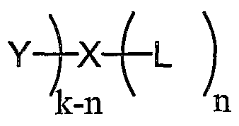


Priority Applications (9)
| Application Number | Priority Date | Filing Date | Title |
|---|---|---|---|
| EP14183926.6A EP2902464B1 (en) | 2002-03-29 | 2003-03-28 | Light emitting device including semiconductor nanocrystals |
| EP03714454A EP1493308A4 (en) | 2002-03-29 | 2003-03-28 | Light emitting device including semiconductor nanocrystals |
| KR1020047015324A KR101058483B1 (en) | 2002-03-29 | 2003-03-28 | Light Emitting Device Containing Semiconductor Nanocrystals |
| EP12171383.8A EP2557139B1 (en) | 2002-03-29 | 2003-03-28 | Light emitting device including semiconductor nanocrystals |
| JP2003581553A JP4948747B2 (en) | 2002-03-29 | 2003-03-28 | Light-emitting devices including semiconductor nanocrystals |
| CN038120704A CN1656856B (en) | 2002-03-29 | 2003-03-28 | Light emitting device including semiconductor nanocrystals |
| AU2003218452A AU2003218452C1 (en) | 2002-03-29 | 2003-03-28 | Light emitting device including semiconductor nanocrystals |
| CA2480518A CA2480518C (en) | 2002-03-29 | 2003-03-28 | Light emitting device including semiconductor nanocrystals |
| AU2009200659A AU2009200659B2 (en) | 2002-03-29 | 2009-02-19 | Light Emitting Device Including Semiconductor Nanocrystals |
Applications Claiming Priority (2)
| Application Number | Priority Date | Filing Date | Title |
|---|---|---|---|
| US36813002P | 2002-03-29 | 2002-03-29 | |
| US60/368,130 | 2002-03-29 |
Publications (1)
| Publication Number | Publication Date |
|---|---|
| WO2003084292A1 true WO2003084292A1 (en) | 2003-10-09 |
Family
ID=28675447
Family Applications (1)
| Application Number | Title | Priority Date | Filing Date |
|---|---|---|---|
| PCT/US2003/009619 WO2003084292A1 (en) | 2002-03-29 | 2003-03-28 | Light emitting device including semiconductor nanocrystals |
Country Status (8)
| Country | Link |
|---|---|
| US (2) | US7700200B2 (en) |
| EP (3) | EP1493308A4 (en) |
| JP (2) | JP4948747B2 (en) |
| KR (1) | KR101058483B1 (en) |
| CN (1) | CN1656856B (en) |
| AU (2) | AU2003218452C1 (en) |
| CA (2) | CA2480518C (en) |
| WO (1) | WO2003084292A1 (en) |
Cited By (30)
| Publication number | Priority date | Publication date | Assignee | Title |
|---|---|---|---|---|
| US6878871B2 (en) | 2002-09-05 | 2005-04-12 | Nanosys, Inc. | Nanostructure and nanocomposite based compositions and photovoltaic devices |
| WO2005055330A1 (en) * | 2003-12-02 | 2005-06-16 | Koninklijke Philips Electronics N.V. | Electroluminescent device |
| WO2005055331A1 (en) * | 2003-12-02 | 2005-06-16 | Koninklijke Philips Electronics N.V. | Pixel arrangement for an emissive device |
| JP2005340195A (en) * | 2004-05-28 | 2005-12-08 | Samsung Electronics Co Ltd | Manufacturing method of nano-crystal multilayered thin film and organic/inorganic hybrid electroluminescent element using the same |
| JP2005353595A (en) * | 2004-06-09 | 2005-12-22 | Samsung Electronics Co Ltd | Nano crystal electroluminescent element and its manufacturing method |
| JP2006066395A (en) * | 2004-08-25 | 2006-03-09 | Samsung Electronics Co Ltd | White luminescence organic/inorganic hybrid electroluminescent element containing semiconductor nanocrystal |
| WO2006047215A3 (en) * | 2004-10-22 | 2006-06-15 | Massachusetts Inst Technology | Method and system for transferring a patterned material |
| US7068898B2 (en) | 2002-09-05 | 2006-06-27 | Nanosys, Inc. | Nanocomposites |
| WO2006076290A1 (en) * | 2005-01-11 | 2006-07-20 | Massachusetts Institute Of Technology | Nanocrystals including iii-v semiconductors |
| US7091120B2 (en) | 2003-08-04 | 2006-08-15 | Nanosys, Inc. | System and process for producing nanowire composites and electronic substrates therefrom |
| JP2007510303A (en) * | 2003-10-29 | 2007-04-19 | コーニンクレッカ フィリップス エレクトロニクス エヌ ヴィ | Light emitting device with improved quantum efficiency |
| JP2007528612A (en) * | 2004-03-08 | 2007-10-11 | マサチューセッツ・インスティテュート・オブ・テクノロジー | Blue light emitting semiconductor nanocrystal material |
| US7700001B2 (en) | 2002-08-23 | 2010-04-20 | Sharp Kabushiki Kaisha | Light-emitting apparatus, phosphor and method of producing it |
| EP2297762A1 (en) * | 2008-05-06 | 2011-03-23 | QD Vision, INC. | Solid state lighting devices including quantum confined semiconductor nanoparticles |
| US8043793B2 (en) | 2007-09-28 | 2011-10-25 | Dai Nippon Printing Co., Ltd. | Method for manufacturing electroluminescence element |
| WO2012013270A1 (en) | 2010-07-26 | 2012-02-02 | Merck Patent Gmbh | Nanocrystals in devices |
| WO2012013272A1 (en) | 2010-07-26 | 2012-02-02 | Merck Patent Gmbh | Quantum dots and hosts |
| WO2014066770A1 (en) | 2012-10-26 | 2014-05-01 | Research Triangle Institute, International | Intermediate band semiconductors, heterojunctions, and optoelectronic devices utilizing solution processed quantum dots, and related methods |
| DE102014100405A1 (en) * | 2014-01-15 | 2015-07-16 | Osram Oled Gmbh | Organic light-emitting device and method for producing an organic light-emitting device |
| US9093657B2 (en) | 2006-02-14 | 2015-07-28 | Massachusetts Institute Of Technology | White light emitting devices |
| US9133388B2 (en) | 2009-04-28 | 2015-09-15 | Qd Vision, Inc. | Optical materials, optical components, and methods |
| EP2774189A4 (en) * | 2011-10-31 | 2015-12-02 | Univ Nanyang Tech | A light-emitting device |
| EP2781574A4 (en) * | 2011-11-18 | 2015-12-02 | Obschestvo S Ogranichennoi Otvetstvennostyu Lumen Ooo Lumen | Luminescent composite material and light-emitting device based thereon |
| US9276048B2 (en) | 2006-09-29 | 2016-03-01 | University Of Florida Research Foundation, Inc. | Method and apparatus for infrared detection and display |
| US9525148B2 (en) | 2008-04-03 | 2016-12-20 | Qd Vision, Inc. | Device including quantum dots |
| DE102007029915B4 (en) | 2006-12-20 | 2017-03-30 | Lg Display Co., Ltd. | Organic electroluminescent device and method of making the same |
| US9997571B2 (en) | 2010-05-24 | 2018-06-12 | University Of Florida Research Foundation, Inc. | Method and apparatus for providing a charge blocking layer on an infrared up-conversion device |
| US10134815B2 (en) | 2011-06-30 | 2018-11-20 | Nanoholdings, Llc | Method and apparatus for detecting infrared radiation with gain |
| US10333090B2 (en) | 2008-04-03 | 2019-06-25 | Samsung Research America, Inc. | Light-emitting device including quantum dots |
| US10749058B2 (en) | 2015-06-11 | 2020-08-18 | University Of Florida Research Foundation, Incorporated | Monodisperse, IR-absorbing nanoparticles and related methods and devices |
Families Citing this family (141)
| Publication number | Priority date | Publication date | Assignee | Title |
|---|---|---|---|---|
| IL146226A0 (en) * | 2001-10-29 | 2002-12-01 | Yissum Res Dev Co | Near infra-red composite polymer-nanocrystal materials and electro-optical devices produced therefrom |
| EP1493308A4 (en) * | 2002-03-29 | 2009-09-16 | Massachusetts Inst Technology | Light emitting device including semiconductor nanocrystals |
| US7279832B2 (en) * | 2003-04-01 | 2007-10-09 | Innovalight, Inc. | Phosphor materials and illumination devices made therefrom |
| WO2005024952A2 (en) * | 2003-09-05 | 2005-03-17 | The University Of North Carolina At Charlotte | Quantum dot optoelectronic devices with nanoscale epitaxial overgrowth and methods of manufacture |
| KR100697511B1 (en) * | 2003-10-21 | 2007-03-20 | 삼성전자주식회사 | Photocurable Semiconductor Nanocrystal, Photocurable Composition for Pattern Formation of Semiconductor Nanocrystal and Method of Patterning Nanocrystal using the same |
| EP1701940B1 (en) * | 2003-12-23 | 2008-05-28 | H.Lundbeck A/S | 2-(1h-indolylsulfanyl)-benzyl amine derivatives as ssri |
| CN1910763A (en) * | 2004-01-23 | 2007-02-07 | Hoya株式会社 | Quantum dot light-emitting device and method for manufacturing same |
| US7773404B2 (en) | 2005-01-07 | 2010-08-10 | Invisage Technologies, Inc. | Quantum dot optical devices with enhanced gain and sensitivity and methods of making same |
| US7742322B2 (en) * | 2005-01-07 | 2010-06-22 | Invisage Technologies, Inc. | Electronic and optoelectronic devices with quantum dot films |
| US7326908B2 (en) * | 2004-04-19 | 2008-02-05 | Edward Sargent | Optically-regulated optical emission using colloidal quantum dot nanocrystals |
| US7746681B2 (en) | 2005-01-07 | 2010-06-29 | Invisage Technologies, Inc. | Methods of making quantum dot films |
| KR100621309B1 (en) * | 2004-04-20 | 2006-09-14 | 삼성전자주식회사 | Method for Preparing Metal Sulfide Nanocrystal Using Thiol Compound As Sulfur Precursor |
| US8129906B1 (en) | 2004-04-26 | 2012-03-06 | Imaging Systems Technology, Inc. | Lumino-shells |
| CA2567930A1 (en) | 2004-06-08 | 2005-12-22 | Nanosys, Inc. | Methods and devices for forming nanostructure monolayers and devices including such monolayers |
| TWI406890B (en) * | 2004-06-08 | 2013-09-01 | Sandisk Corp | Post-deposition encapsulation of nanostructures : compositions, devices and systems incorporating same |
| US8088483B1 (en) | 2004-06-08 | 2012-01-03 | Nanosys, Inc. | Process for group 10 metal nanostructure synthesis and compositions made using same |
| US8563133B2 (en) | 2004-06-08 | 2013-10-22 | Sandisk Corporation | Compositions and methods for modulation of nanostructure energy levels |
| US7968273B2 (en) | 2004-06-08 | 2011-06-28 | Nanosys, Inc. | Methods and devices for forming nanostructure monolayers and devices including such monolayers |
| US7776758B2 (en) | 2004-06-08 | 2010-08-17 | Nanosys, Inc. | Methods and devices for forming nanostructure monolayers and devices including such monolayers |
| US20070045777A1 (en) * | 2004-07-08 | 2007-03-01 | Jennifer Gillies | Micronized semiconductor nanocrystal complexes and methods of making and using same |
| AR052308A1 (en) * | 2004-07-16 | 2007-03-14 | Lundbeck & Co As H | DERIVATIVES OF 2- (1H-INDOLILSULFANIL) -ARILAMINE AND A PHARMACEUTICAL COMPOSITION CONTAINING THE COMPOUND |
| US7557028B1 (en) | 2004-07-28 | 2009-07-07 | Nanosys, Inc. | Process for group III-V semiconductor nanostructure synthesis and compositions made using same |
| US7750352B2 (en) * | 2004-08-10 | 2010-07-06 | Pinion Technologies, Inc. | Light strips for lighting and backlighting applications |
| WO2006137924A2 (en) | 2004-11-03 | 2006-12-28 | Massachusetts Institute Of Technology | Light emitting device |
| US7799422B2 (en) * | 2004-11-03 | 2010-09-21 | Massachusetts Institute Of Technology | Absorbing film |
| US8891575B2 (en) * | 2004-11-30 | 2014-11-18 | Massachusetts Institute Of Technology | Optical feedback structures and methods of making |
| WO2006060660A2 (en) * | 2004-12-01 | 2006-06-08 | Cornell Research Foundation, Inc. | Group iii nitride coatings and methods |
| US7772288B2 (en) | 2004-12-01 | 2010-08-10 | Cornell Research Foundation, Inc. | Group III nitride coatings and methods |
| CA2519608A1 (en) | 2005-01-07 | 2006-07-07 | Edward Sargent | Quantum dot-polymer nanocomposite photodetectors and photovoltaics |
| US7811479B2 (en) * | 2005-02-07 | 2010-10-12 | The Trustees Of The University Of Pennsylvania | Polymer-nanocrystal quantum dot composites and optoelectronic devices |
| EP1864341B1 (en) * | 2005-02-16 | 2019-11-13 | Massachusetts Institute Of Technology | Light emitting device including semiconductor nanocrystals |
| US20090039764A1 (en) * | 2005-03-17 | 2009-02-12 | Cho Kyung Sang | Quantum Dot Light-Emitting Diode Comprising Inorganic Electron Transport Layer |
| JP2008534424A (en) * | 2005-03-31 | 2008-08-28 | エージェンシー フォー サイエンス、テクノロジー アンド リサーチ | CDTE / GSH core-shell quantum dots |
| US9297092B2 (en) * | 2005-06-05 | 2016-03-29 | Qd Vision, Inc. | Compositions, optical component, system including an optical component, devices, and other products |
| US8845927B2 (en) * | 2006-06-02 | 2014-09-30 | Qd Vision, Inc. | Functionalized nanoparticles and method |
| AR054393A1 (en) * | 2005-06-17 | 2007-06-20 | Lundbeck & Co As H | DERIVATIVES OF BENZO (B) FURANO AND BENZO (B) THIOPHEN, PHARMACEUTICAL COMPOSITIONS CONTAINING THEM AND THEIR USE IN THE MANUFACTURE OF A MEDICINAL PRODUCT FOR THE TREATMENT OF DISEASES MEDIATED BY THE INHIBITION OF THE REINFORCEMENT OF AMINA BOSS NEUTRANTS. |
| US7629473B2 (en) * | 2005-06-17 | 2009-12-08 | H. Lundbeck A/S | 2-(1H-indolylsulfanyl)-aryl amine derivatives |
| US20070001581A1 (en) * | 2005-06-29 | 2007-01-04 | Stasiak James W | Nanostructure based light emitting devices and associated methods |
| KR20070035341A (en) * | 2005-09-27 | 2007-03-30 | 삼성전자주식회사 | Light emitting device including void passivation semiconductor nanocrystal layer and process for preparing the same |
| KR101304635B1 (en) * | 2006-01-09 | 2013-09-05 | 삼성전자주식회사 | Inorganic electroluminescent diode and process for preparing the same |
| WO2007092606A2 (en) * | 2006-02-09 | 2007-08-16 | Qd Vision, Inc. | Displays including semiconductor nanocrystals and methods of making same |
| EP1999797A4 (en) * | 2006-02-09 | 2010-11-24 | Qd Vision Inc | Device including semiconductor nanocrystals and a layer including a doped organic material and methods |
| KR20080103568A (en) * | 2006-02-17 | 2008-11-27 | 솔렉슨트 코포레이션 | Nanostructured electroluminescent device and display |
| US9701899B2 (en) | 2006-03-07 | 2017-07-11 | Samsung Electronics Co., Ltd. | Compositions, optical component, system including an optical component, devices, and other products |
| WO2008070028A2 (en) * | 2006-12-01 | 2008-06-12 | Qd Vision, Inc. | Improved composites and devices including nanoparticles |
| WO2007143197A2 (en) | 2006-06-02 | 2007-12-13 | Qd Vision, Inc. | Light-emitting devices and displays with improved performance |
| US8849087B2 (en) * | 2006-03-07 | 2014-09-30 | Qd Vision, Inc. | Compositions, optical component, system including an optical component, devices, and other products |
| US9951438B2 (en) * | 2006-03-07 | 2018-04-24 | Samsung Electronics Co., Ltd. | Compositions, optical component, system including an optical component, devices, and other products |
| WO2007117698A2 (en) * | 2006-04-07 | 2007-10-18 | Qd Vision, Inc. | Composition including material, methods of depositing material, articles including same and systems for depositing material |
| WO2007120877A2 (en) * | 2006-04-14 | 2007-10-25 | Qd Vision, Inc. | Transfer surface for manufacturing a light emitting device |
| US8941299B2 (en) * | 2006-05-21 | 2015-01-27 | Massachusetts Institute Of Technology | Light emitting device including semiconductor nanocrystals |
| US9212056B2 (en) * | 2006-06-02 | 2015-12-15 | Qd Vision, Inc. | Nanoparticle including multi-functional ligand and method |
| WO2008111947A1 (en) * | 2006-06-24 | 2008-09-18 | Qd Vision, Inc. | Methods and articles including nanomaterial |
| WO2008108798A2 (en) * | 2006-06-24 | 2008-09-12 | Qd Vision, Inc. | Methods for depositing nanomaterial, methods for fabricating a device, and methods for fabricating an array of devices |
| WO2008105792A2 (en) * | 2006-06-24 | 2008-09-04 | Qd Vision, Inc. | Methods for depositing nanomaterial, methods for fabricating a device, methods for fabricating an array of devices and compositions |
| US11031567B2 (en) * | 2006-07-11 | 2021-06-08 | The Regents Of The University Of Michigan | Efficient solar cells using all-organic nanocrystalline networks |
| US8643058B2 (en) * | 2006-07-31 | 2014-02-04 | Massachusetts Institute Of Technology | Electro-optical device including nanocrystals |
| WO2008021962A2 (en) | 2006-08-11 | 2008-02-21 | Massachusetts Institute Of Technology | Blue light emitting semiconductor nanocrystals and devices |
| KR101282400B1 (en) * | 2006-08-24 | 2013-07-04 | 한국과학기술원 | Organic light emitting diode display |
| WO2008085210A2 (en) * | 2006-09-12 | 2008-07-17 | Qd Vision, Inc. | Electroluminescent display useful for displaying a predetermined pattern |
| WO2008033388A2 (en) * | 2006-09-12 | 2008-03-20 | Qd Vision, Inc. | A composite including nanoparticles, methods, and products including a composite |
| US7393618B2 (en) | 2006-09-15 | 2008-07-01 | Idemitsu Kosan Co., Ltd. | Composition for color converting member and production method of color conversion substrate using the same |
| WO2008063652A1 (en) * | 2006-11-21 | 2008-05-29 | Qd Vision, Inc. | Blue emitting semiconductor nanocrystals and compositions and devices including same |
| WO2008063653A1 (en) | 2006-11-21 | 2008-05-29 | Qd Vision, Inc. | Semiconductor nanocrystals and compositions and devices including same |
| WO2008133660A2 (en) * | 2006-11-21 | 2008-11-06 | Qd Vision, Inc. | Nanocrystals including a group iiia element and a group va element, method, composition, device and other prodcucts |
| WO2008063657A2 (en) * | 2006-11-21 | 2008-05-29 | Qd Vision, Inc. | Light emitting devices and displays with improved performance |
| WO2008063658A2 (en) | 2006-11-21 | 2008-05-29 | Qd Vision, Inc. | Semiconductor nanocrystals and compositions and devices including same |
| KR100864882B1 (en) * | 2006-12-28 | 2008-10-22 | 삼성에스디아이 주식회사 | OLED Display Device and fabricating method of the same |
| US20080172197A1 (en) * | 2007-01-11 | 2008-07-17 | Motorola, Inc. | Single laser multi-color projection display with quantum dot screen |
| WO2008120603A1 (en) * | 2007-03-30 | 2008-10-09 | Idemitsu Kosan Co., Ltd. | Light emitting element |
| US10043993B2 (en) * | 2007-06-25 | 2018-08-07 | Massachusetts Institute Of Technology | Electro-optical device |
| EP2165354B1 (en) | 2007-06-25 | 2018-05-30 | Massachusetts Institute of Technology | Photovoltaic device including semiconductor nanocrystals |
| KR101672553B1 (en) | 2007-06-25 | 2016-11-03 | 큐디 비젼, 인크. | Compositions and methods including depositing nanomaterial |
| WO2009002551A1 (en) * | 2007-06-26 | 2008-12-31 | Qd Vision, Inc. | Photovoltaic devices including quantum dot down-conversion materials useful for solar cells and materials including quantum dots |
| EP2165185B1 (en) | 2007-06-26 | 2015-08-19 | Massachusetts Institute of Technology | Controlled modification of semiconductor nanocrystals |
| US9136498B2 (en) * | 2007-06-27 | 2015-09-15 | Qd Vision, Inc. | Apparatus and method for modulating photon output of a quantum dot light emitting device |
| JP5277588B2 (en) * | 2007-08-21 | 2013-08-28 | 東ソー株式会社 | Organic EL device |
| JP2009087781A (en) * | 2007-09-28 | 2009-04-23 | Dainippon Printing Co Ltd | Electroluminescent element and its manufacturing method |
| JP2009087782A (en) * | 2007-09-28 | 2009-04-23 | Dainippon Printing Co Ltd | Manufacturing method of electroluminescent element |
| JP2009087783A (en) | 2007-09-28 | 2009-04-23 | Dainippon Printing Co Ltd | Electroluminescent element |
| JP5176459B2 (en) * | 2007-09-28 | 2013-04-03 | 大日本印刷株式会社 | White light emitting device |
| WO2009072288A1 (en) * | 2007-12-06 | 2009-06-11 | Panasonic Corporation | Light-emitting device and display device using the same |
| US20110079273A1 (en) * | 2008-01-10 | 2011-04-07 | Massachusetts Institute Of Technology | Photovoltaic devices |
| WO2009089470A2 (en) * | 2008-01-11 | 2009-07-16 | Massachusetts Institute Of Technology | Photovoltaic devices |
| WO2009099425A2 (en) | 2008-02-07 | 2009-08-13 | Qd Vision, Inc. | Flexible devices including semiconductor nanocrystals, arrays, and methods |
| JP5118503B2 (en) * | 2008-02-21 | 2013-01-16 | パナソニック株式会社 | Light emitting element |
| JP5118504B2 (en) * | 2008-02-21 | 2013-01-16 | パナソニック株式会社 | Light emitting element |
| US9207385B2 (en) | 2008-05-06 | 2015-12-08 | Qd Vision, Inc. | Lighting systems and devices including same |
| WO2009137053A1 (en) | 2008-05-06 | 2009-11-12 | Qd Vision, Inc. | Optical components, systems including an optical component, and devices |
| CN101887946B (en) * | 2009-05-14 | 2014-09-17 | 群创光电股份有限公司 | Manufacturing method of organic electroluminescent device and its image display system |
| US8106420B2 (en) * | 2009-06-05 | 2012-01-31 | Massachusetts Institute Of Technology | Light emitting device including semiconductor nanocrystals |
| CN105713599B (en) | 2009-08-14 | 2018-09-11 | 三星电子株式会社 | Luminescent device, optical element and method for luminescent device |
| CN102005443B (en) * | 2009-09-02 | 2014-02-19 | 鸿富锦精密工业(深圳)有限公司 | Light-emitting diode (LED) packaging structure and manufacturing method thereof |
| WO2011037042A1 (en) | 2009-09-28 | 2011-03-31 | 株式会社 村田製作所 | Method for producing nanoparticle material, nanoparticle material, and photoelectric conversion device |
| WO2011047385A1 (en) | 2009-10-17 | 2011-04-21 | Qd Vision, Inc. | An optical, component, products including same, and methods for making same |
| KR101924080B1 (en) | 2009-11-11 | 2018-11-30 | 삼성 리서치 아메리카 인코포레이티드 | Device including quantum dots |
| GB2480323A (en) * | 2010-05-14 | 2011-11-16 | Cambridge Display Tech Ltd | OLED hole transport layer |
| JP5944380B2 (en) * | 2010-05-27 | 2016-07-05 | メルク パテント ゲーエムベーハー | Composition comprising quantum dots |
| US9214639B2 (en) | 2010-06-24 | 2015-12-15 | Massachusetts Institute Of Technology | Conductive polymer on a textured or plastic substrate |
| WO2011163556A2 (en) | 2010-06-24 | 2011-12-29 | Massachusetts Institute Of Technology | Conductive polymer on a textured or plastic substrate |
| WO2012091778A2 (en) * | 2010-10-01 | 2012-07-05 | Intelligent Material Solutions, Inc. | Morphologically and size uniform monodisperse particles and their shape-directed self-assembly |
| WO2012134629A1 (en) | 2011-04-01 | 2012-10-04 | Qd Vision, Inc. | Quantum dots, method, and devices |
| WO2013019299A2 (en) | 2011-05-11 | 2013-02-07 | Qd Vision, Inc. | Method for processing devices including quantum dots and devices |
| US8508830B1 (en) | 2011-05-13 | 2013-08-13 | Google Inc. | Quantum dot near-to-eye display |
| WO2012158832A2 (en) | 2011-05-16 | 2012-11-22 | Qd Vision, Inc. | Method for preparing semiconductor nanocrystals |
| US9520573B2 (en) | 2011-05-16 | 2016-12-13 | Qd Vision, Inc. | Device including quantum dots and method for making same |
| KR20130000218A (en) * | 2011-06-22 | 2013-01-02 | 삼성디스플레이 주식회사 | Electrode including magnetic material and organic light emitting device using the electrode |
| US9252377B2 (en) * | 2011-07-14 | 2016-02-02 | Universal Display Corporation | Inorganic hosts in OLEDs |
| WO2013028253A1 (en) | 2011-08-19 | 2013-02-28 | Qd Vision, Inc. | Semiconductor nanocrystals and methods |
| WO2013103440A1 (en) | 2012-01-06 | 2013-07-11 | Qd Vision, Inc. | Light emitting device including blue emitting quantum dots and method |
| JP6223417B2 (en) * | 2012-03-19 | 2017-11-01 | ネクスドット | Light emitting device including anisotropic flat colloidal semiconductor nanocrystal and method for manufacturing the same |
| FR2988223B1 (en) | 2012-03-19 | 2016-09-02 | Solarwell | LIGHT EMITTING DEVICE CONTAINING APLATISED ANISOTROPIC SEMICONDUCTOR COLLOIDAL NANOCRISTALS AND PROCESS FOR PRODUCING SUCH DEVICES |
| US9929325B2 (en) | 2012-06-05 | 2018-03-27 | Samsung Electronics Co., Ltd. | Lighting device including quantum dots |
| US9024526B1 (en) | 2012-06-11 | 2015-05-05 | Imaging Systems Technology, Inc. | Detector element with antenna |
| US9139770B2 (en) | 2012-06-22 | 2015-09-22 | Nanosys, Inc. | Silicone ligands for stabilizing quantum dot films |
| TWI596188B (en) | 2012-07-02 | 2017-08-21 | 奈米系統股份有限公司 | Highly luminescent nanostructures and methods of producing same |
| US20140203259A1 (en) * | 2013-01-18 | 2014-07-24 | Universal Display Corporation | Host for organic light emitting devices |
| WO2014159927A2 (en) | 2013-03-14 | 2014-10-02 | Nanosys, Inc. | Method for solventless quantum dot exchange |
| CA2948486A1 (en) * | 2014-05-09 | 2015-11-12 | Massachusetts Institute Of Technology | Energy level modification of nanocrystals through ligand exchange |
| US10593821B2 (en) | 2014-09-12 | 2020-03-17 | Board Of Regents, The University Of Texas System | Photonic curing of nanocrystal films for photovoltaics |
| US11205757B2 (en) * | 2014-11-06 | 2021-12-21 | Sn Display Co., Ltd. | Core-shell structured perovskite particle light-emitter, method of preparing the same and light emitting device using the same |
| US10597580B2 (en) | 2015-10-28 | 2020-03-24 | Samsung Electronics Co., Ltd. | Quantum dots, production methods thereof, and electronic devices including the same |
| US10273403B2 (en) | 2016-05-31 | 2019-04-30 | Alliance For Sustainable Energy, Llc | Nanoparticles for photovoltaic and LED devices and methods of making the same |
| US10544168B2 (en) | 2016-06-15 | 2020-01-28 | Alliance For Sustainable Energy, Llc | Ligand-exchangeable nanoparticles and methods of making the same |
| EP3410208A1 (en) | 2017-06-01 | 2018-12-05 | Evonik Degussa GmbH | Device containing metal oxide-containing layers |
| EP3409813A1 (en) | 2017-06-01 | 2018-12-05 | Evonik Degussa GmbH | Device containing metal oxide-containing layers |
| CN108346750B (en) * | 2017-08-08 | 2019-07-19 | 广东聚华印刷显示技术有限公司 | Electroluminescent device and its luminescent layer and application |
| KR20190043085A (en) | 2017-10-17 | 2019-04-25 | 엘지디스플레이 주식회사 | Luminous body, light emitting film, light emitting diode and light emitting device having the luminous body |
| US11121339B2 (en) * | 2018-05-11 | 2021-09-14 | Nanosys, Inc. | Quantum dot LED design based on resonant energy transfer |
| CN108878635B (en) * | 2018-06-07 | 2020-10-30 | 上海大学 | N-type PbSe-PbS-based thermoelectric material and preparation method thereof |
| CN109037463A (en) * | 2018-07-21 | 2018-12-18 | 戚明海 | A kind of OLED and its manufacturing method with fluorescent particles |
| KR20200023243A (en) | 2018-08-23 | 2020-03-04 | 삼성전자주식회사 | Quantum dot device and quantum dots |
| US10851298B2 (en) | 2018-08-30 | 2020-12-01 | Samsung Electronics Co., Ltd. | Electronic device including quantum dots |
| US20220158108A1 (en) * | 2019-02-27 | 2022-05-19 | Sharp Kabushiki Kaisha | Light-emitting element and display device using light-emitting element |
| US20220127286A1 (en) | 2019-03-04 | 2022-04-28 | Merck Patent Gmbh | Ligands for nano-sized materials |
| KR20210027211A (en) | 2019-08-29 | 2021-03-10 | 삼성전자주식회사 | Quantum dots and device including the same |
| EP3809474B1 (en) | 2019-10-18 | 2023-07-19 | Samsung Electronics Co., Ltd. | Quantum dot light-emitting device and electronic device |
| US20220407024A1 (en) | 2019-10-28 | 2022-12-22 | Fraunhofer-Gesellischaft Zur Forderung Der Angewandten Forschung E.V. | Method for producing a light-emitting diode having polarized emission |
| KR20210076744A (en) | 2019-12-16 | 2021-06-24 | 삼성전자주식회사 | Light-emitting device and production method thereof |
| KR20220003356A (en) | 2020-07-01 | 2022-01-10 | 삼성전자주식회사 | Light emitting device and display device including the same |
| KR20220042933A (en) * | 2020-09-28 | 2022-04-05 | 삼성전자주식회사 | Method for manufacturing light-emitting material, light-emitting manufactured thereby and light-emitting device comprising same |
Citations (5)
| Publication number | Priority date | Publication date | Assignee | Title |
|---|---|---|---|---|
| US5537000A (en) * | 1994-04-29 | 1996-07-16 | The Regents, University Of California | Electroluminescent devices formed using semiconductor nanocrystals as an electron transport media and method of making such electroluminescent devices |
| US5677545A (en) * | 1994-09-12 | 1997-10-14 | Motorola | Organic light emitting diodes with molecular alignment and method of fabrication |
| US6157047A (en) * | 1997-08-29 | 2000-12-05 | Kabushiki Kaisha Toshiba | Light emitting semiconductor device using nanocrystals |
| US6322901B1 (en) | 1997-11-13 | 2001-11-27 | Massachusetts Institute Of Technology | Highly luminescent color-selective nano-crystalline materials |
| US6447698B1 (en) * | 1998-09-28 | 2002-09-10 | Sony Corporation | Method for producing light-emitting substance |
Family Cites Families (31)
| Publication number | Priority date | Publication date | Assignee | Title |
|---|---|---|---|---|
| JP3125332B2 (en) | 1991-06-21 | 2001-01-15 | ソニー株式会社 | Quantum dot tunnel device, information processing device and information processing method using the same |
| US5505928A (en) | 1991-11-22 | 1996-04-09 | The Regents Of University Of California | Preparation of III-V semiconductor nanocrystals |
| EP0613585A4 (en) | 1991-11-22 | 1995-06-21 | Univ California | Semiconductor nanocrystals covalently bound to solid inorganic surfaces using self-assembled monolayers. |
| US5260957A (en) | 1992-10-29 | 1993-11-09 | The Charles Stark Draper Laboratory, Inc. | Quantum dot Laser |
| US5293050A (en) | 1993-03-25 | 1994-03-08 | International Business Machines Corporation | Semiconductor quantum dot light emitting/detecting devices |
| US6048616A (en) | 1993-04-21 | 2000-04-11 | Philips Electronics N.A. Corp. | Encapsulated quantum sized doped semiconductor particles and method of manufacturing same |
| US5422489A (en) | 1994-01-24 | 1995-06-06 | Bhargava; Rameshwar N. | Light emitting device |
| WO1996010282A1 (en) | 1994-09-29 | 1996-04-04 | British Telecommunications Public Limited Company | Optical fibre with quantum dots |
| US5585640A (en) | 1995-01-11 | 1996-12-17 | Huston; Alan L. | Glass matrix doped with activated luminescent nanocrystalline particles |
| GB9518910D0 (en) | 1995-09-15 | 1995-11-15 | Imperial College | Process |
| US6103868A (en) | 1996-12-27 | 2000-08-15 | The Regents Of The University Of California | Organically-functionalized monodisperse nanocrystals of metals |
| US5958573A (en) * | 1997-02-10 | 1999-09-28 | Quantum Energy Technologies | Electroluminescent device having a structured particle electron conductor |
| US6607829B1 (en) | 1997-11-13 | 2003-08-19 | Massachusetts Institute Of Technology | Tellurium-containing nanocrystalline materials |
| US6236060B1 (en) * | 1997-11-19 | 2001-05-22 | International Business Machines Corporation | Light emitting structures in back-end of line silicon technology |
| US6501091B1 (en) * | 1998-04-01 | 2002-12-31 | Massachusetts Institute Of Technology | Quantum dot white and colored light emitting diodes |
| US6864626B1 (en) | 1998-06-03 | 2005-03-08 | The Regents Of The University Of California | Electronic displays using optically pumped luminescent semiconductor nanocrystals |
| US6294401B1 (en) | 1998-08-19 | 2001-09-25 | Massachusetts Institute Of Technology | Nanoparticle-based electrical, chemical, and mechanical structures and methods of making same |
| JP4404489B2 (en) * | 1998-09-18 | 2010-01-27 | マサチューセッツ インスティテュート オブ テクノロジー | Water-soluble fluorescent semiconductor nanocrystal |
| JP4425470B2 (en) * | 1998-09-18 | 2010-03-03 | マサチューセッツ インスティテュート オブ テクノロジー | Biological applications of semiconductor nanocrystals |
| US6251303B1 (en) | 1998-09-18 | 2001-06-26 | Massachusetts Institute Of Technology | Water-soluble fluorescent nanocrystals |
| JP2001279240A (en) * | 2000-03-29 | 2001-10-10 | Toshiba Corp | Illuminant particle and light-emitting device |
| US6797412B1 (en) | 2000-04-11 | 2004-09-28 | University Of Connecticut | Full color display structures using pseudomorphic cladded quantum dot nanophosphor thin films |
| US6576291B2 (en) | 2000-12-08 | 2003-06-10 | Massachusetts Institute Of Technology | Preparation of nanocrystallites |
| US6846565B2 (en) | 2001-07-02 | 2005-01-25 | Board Of Regents, The University Of Texas System | Light-emitting nanoparticles and method of making same |
| EP2218762A3 (en) | 2001-07-20 | 2010-09-29 | Life Technologies Corporation | Luminescent nanoparticles and methods for their preparation |
| WO2003021694A2 (en) | 2001-09-04 | 2003-03-13 | Koninklijke Philips Electronics N.V. | Electroluminescent device comprising quantum dots |
| EP1438614B1 (en) * | 2001-09-17 | 2009-05-13 | Massachusetts Institute Of Technology | Semiconductor nanocrystal composite |
| EP1493308A4 (en) * | 2002-03-29 | 2009-09-16 | Massachusetts Inst Technology | Light emitting device including semiconductor nanocrystals |
| WO2005017951A2 (en) | 2002-08-02 | 2005-02-24 | Ultradots, Inc. | Quantum dots, nanocomposite materials with quantum dots, optical devices with quantum dots, and related fabrication methods |
| US7332211B1 (en) * | 2002-11-07 | 2008-02-19 | Massachusetts Institute Of Technology | Layered materials including nanoparticles |
| US20040265622A1 (en) | 2003-06-24 | 2004-12-30 | Eastman Kodak Company | Light emitting display |
-
2003
- 2003-03-28 EP EP03714454A patent/EP1493308A4/en not_active Withdrawn
- 2003-03-28 CA CA2480518A patent/CA2480518C/en not_active Expired - Lifetime
- 2003-03-28 CN CN038120704A patent/CN1656856B/en not_active Expired - Lifetime
- 2003-03-28 EP EP14183926.6A patent/EP2902464B1/en not_active Expired - Lifetime
- 2003-03-28 AU AU2003218452A patent/AU2003218452C1/en not_active Expired
- 2003-03-28 KR KR1020047015324A patent/KR101058483B1/en active IP Right Grant
- 2003-03-28 EP EP12171383.8A patent/EP2557139B1/en not_active Expired - Lifetime
- 2003-03-28 WO PCT/US2003/009619 patent/WO2003084292A1/en active Application Filing
- 2003-03-28 JP JP2003581553A patent/JP4948747B2/en not_active Expired - Lifetime
- 2003-03-28 US US10/400,908 patent/US7700200B2/en active Active
- 2003-03-28 CA CA2934970A patent/CA2934970C/en not_active Expired - Lifetime
-
2009
- 2009-02-19 AU AU2009200659A patent/AU2009200659B2/en not_active Expired
-
2010
- 2010-03-05 US US12/718,596 patent/US20100240901A1/en not_active Abandoned
- 2010-07-29 JP JP2010170272A patent/JP5463234B2/en not_active Expired - Lifetime
Patent Citations (5)
| Publication number | Priority date | Publication date | Assignee | Title |
|---|---|---|---|---|
| US5537000A (en) * | 1994-04-29 | 1996-07-16 | The Regents, University Of California | Electroluminescent devices formed using semiconductor nanocrystals as an electron transport media and method of making such electroluminescent devices |
| US5677545A (en) * | 1994-09-12 | 1997-10-14 | Motorola | Organic light emitting diodes with molecular alignment and method of fabrication |
| US6157047A (en) * | 1997-08-29 | 2000-12-05 | Kabushiki Kaisha Toshiba | Light emitting semiconductor device using nanocrystals |
| US6322901B1 (en) | 1997-11-13 | 2001-11-27 | Massachusetts Institute Of Technology | Highly luminescent color-selective nano-crystalline materials |
| US6447698B1 (en) * | 1998-09-28 | 2002-09-10 | Sony Corporation | Method for producing light-emitting substance |
Non-Patent Citations (1)
| Title |
|---|
| See also references of EP1493308A4 |
Cited By (62)
| Publication number | Priority date | Publication date | Assignee | Title |
|---|---|---|---|---|
| US8287760B2 (en) | 2002-08-23 | 2012-10-16 | Sharp Kabushiki Kaisha | Light-emitting apparatus, phosphorescent portion, and method of producing the same |
| US7700001B2 (en) | 2002-08-23 | 2010-04-20 | Sharp Kabushiki Kaisha | Light-emitting apparatus, phosphor and method of producing it |
| US8041171B2 (en) | 2002-09-05 | 2011-10-18 | Nanosys, Inc. | Nanocomposites |
| US6878871B2 (en) | 2002-09-05 | 2005-04-12 | Nanosys, Inc. | Nanostructure and nanocomposite based compositions and photovoltaic devices |
| US7603003B2 (en) | 2002-09-05 | 2009-10-13 | Nanosys, Inc | Nanocomposites |
| US7228050B1 (en) | 2002-09-05 | 2007-06-05 | Nanosys, Inc. | Nanocomposites |
| US7068898B2 (en) | 2002-09-05 | 2006-06-27 | Nanosys, Inc. | Nanocomposites |
| US7087832B2 (en) | 2002-09-05 | 2006-08-08 | Nanosys, Inc. | Nanostructure and nanocomposite based compositions and photovoltaic devices |
| US7087833B2 (en) | 2002-09-05 | 2006-08-08 | Nanosys, Inc. | Nanostructure and nanocomposite based compositions and photovoltaic devices |
| US7750235B2 (en) | 2002-09-05 | 2010-07-06 | Nanosys, Inc. | Nanostructure and nanocomposite based compositions and photovoltaic devices |
| US7795125B2 (en) | 2003-08-04 | 2010-09-14 | Nanosys, Inc. | System and process for producing nanowire composites and electronic substrates therefrom |
| US7468315B2 (en) | 2003-08-04 | 2008-12-23 | Nanosys, Inc. | System and process for producing nanowire composites and electronic substrates therefrom |
| US7091120B2 (en) | 2003-08-04 | 2006-08-15 | Nanosys, Inc. | System and process for producing nanowire composites and electronic substrates therefrom |
| KR101112061B1 (en) * | 2003-10-29 | 2012-03-08 | 코닌클리즈케 필립스 일렉트로닉스 엔.브이. | Light-emitting device with increased quantum efficiency |
| JP2007510303A (en) * | 2003-10-29 | 2007-04-19 | コーニンクレッカ フィリップス エレクトロニクス エヌ ヴィ | Light emitting device with improved quantum efficiency |
| JP2007513478A (en) * | 2003-12-02 | 2007-05-24 | コーニンクレッカ フィリップス エレクトロニクス エヌ ヴィ | Electroluminescent device |
| WO2005055331A1 (en) * | 2003-12-02 | 2005-06-16 | Koninklijke Philips Electronics N.V. | Pixel arrangement for an emissive device |
| WO2005055330A1 (en) * | 2003-12-02 | 2005-06-16 | Koninklijke Philips Electronics N.V. | Electroluminescent device |
| JP2007528612A (en) * | 2004-03-08 | 2007-10-11 | マサチューセッツ・インスティテュート・オブ・テクノロジー | Blue light emitting semiconductor nanocrystal material |
| US8440254B2 (en) | 2004-05-28 | 2013-05-14 | Samsung Electronics Co., Ltd. | Method for preparing multilayer of nanocrystals, and organic-inorganic hybrid electroluminescence device comprising multilayer of nanocrystals prepared by the method |
| US7569248B2 (en) | 2004-05-28 | 2009-08-04 | Samsung Electronics Co., Ltd. | Method for preparing multilayer of nanocrystals, and organic-inorganic hybrid electroluminescence device comprising multilayer of nanocrystals prepared by the method |
| US8188650B2 (en) | 2004-05-28 | 2012-05-29 | Samsung Electronics Co., Ltd. | Method for preparing multilayer of nanocrystals, and organic-inorganic hybrid electroluminescence device comprising multilayer of nanocrystals prepared by the method |
| US9598634B2 (en) | 2004-05-28 | 2017-03-21 | Samsung Electronics Co., Ltd. | Method for preparing multilayer of nanocrystals, and organic-inorganic hybrid electroluminescence device comprising multilayer of nanocrystals prepared by the method |
| US10920134B2 (en) | 2004-05-28 | 2021-02-16 | Samsung Electronics Co., Ltd. | Method for preparing multilayer of nanocrystals, and organic-inorganic hybrid electroluminescence device comprising multilayer of nanocrystals prepared by the method |
| JP2005340195A (en) * | 2004-05-28 | 2005-12-08 | Samsung Electronics Co Ltd | Manufacturing method of nano-crystal multilayered thin film and organic/inorganic hybrid electroluminescent element using the same |
| JP2012038741A (en) * | 2004-06-09 | 2012-02-23 | Samsung Electronics Co Ltd | Manufacturing method for nanocrystal electroluminescent element |
| KR100736521B1 (en) | 2004-06-09 | 2007-07-06 | 삼성전자주식회사 | Nanocrystal electroluminescence device and preparation method thereof |
| US8440480B2 (en) | 2004-06-09 | 2013-05-14 | Samsung Electronics Co., Ltd. | Method for fabricating an electroluminescence device |
| JP2005353595A (en) * | 2004-06-09 | 2005-12-22 | Samsung Electronics Co Ltd | Nano crystal electroluminescent element and its manufacturing method |
| US8012781B2 (en) | 2004-06-09 | 2011-09-06 | Samsung Electronics Co., Ltd. | Method for fabricating an electroluminescence device |
| JP2006066395A (en) * | 2004-08-25 | 2006-03-09 | Samsung Electronics Co Ltd | White luminescence organic/inorganic hybrid electroluminescent element containing semiconductor nanocrystal |
| US10225906B2 (en) | 2004-10-22 | 2019-03-05 | Massachusetts Institute Of Technology | Light emitting device including semiconductor nanocrystals |
| EP2498274A1 (en) * | 2004-10-22 | 2012-09-12 | Massachusetts Institute of Technology | Method and system for transferring a patterned material |
| WO2006047215A3 (en) * | 2004-10-22 | 2006-06-15 | Massachusetts Inst Technology | Method and system for transferring a patterned material |
| JP2012142296A (en) * | 2004-10-22 | 2012-07-26 | Massachusetts Institute Of Technology | Light-emitting device including semiconductor nanocrystals |
| US8748933B2 (en) | 2005-01-11 | 2014-06-10 | Massachusetts Institute Of Technology | Nanocrystals including III-V semiconductors |
| WO2006076290A1 (en) * | 2005-01-11 | 2006-07-20 | Massachusetts Institute Of Technology | Nanocrystals including iii-v semiconductors |
| US8134175B2 (en) | 2005-01-11 | 2012-03-13 | Massachusetts Institute Of Technology | Nanocrystals including III-V semiconductors |
| US9093657B2 (en) | 2006-02-14 | 2015-07-28 | Massachusetts Institute Of Technology | White light emitting devices |
| US10700141B2 (en) | 2006-09-29 | 2020-06-30 | University Of Florida Research Foundation, Incorporated | Method and apparatus for infrared detection and display |
| US9276048B2 (en) | 2006-09-29 | 2016-03-01 | University Of Florida Research Foundation, Inc. | Method and apparatus for infrared detection and display |
| DE102007029915B4 (en) | 2006-12-20 | 2017-03-30 | Lg Display Co., Ltd. | Organic electroluminescent device and method of making the same |
| US8043793B2 (en) | 2007-09-28 | 2011-10-25 | Dai Nippon Printing Co., Ltd. | Method for manufacturing electroluminescence element |
| US10333090B2 (en) | 2008-04-03 | 2019-06-25 | Samsung Research America, Inc. | Light-emitting device including quantum dots |
| US11005058B2 (en) | 2008-04-03 | 2021-05-11 | Samsung Research America, Inc. | Light-emitting device including quantum dots |
| US10164205B2 (en) | 2008-04-03 | 2018-12-25 | Samsung Research America, Inc. | Device including quantum dots |
| US9525148B2 (en) | 2008-04-03 | 2016-12-20 | Qd Vision, Inc. | Device including quantum dots |
| EP2297762A1 (en) * | 2008-05-06 | 2011-03-23 | QD Vision, INC. | Solid state lighting devices including quantum confined semiconductor nanoparticles |
| EP2297762A4 (en) * | 2008-05-06 | 2011-11-30 | Qd Vision Inc | Solid state lighting devices including quantum confined semiconductor nanoparticles |
| US9133388B2 (en) | 2009-04-28 | 2015-09-15 | Qd Vision, Inc. | Optical materials, optical components, and methods |
| US9905724B2 (en) | 2009-04-28 | 2018-02-27 | Samsung Electronics Co., Ltd. | Optical materials, optical components, and methods |
| US9997571B2 (en) | 2010-05-24 | 2018-06-12 | University Of Florida Research Foundation, Inc. | Method and apparatus for providing a charge blocking layer on an infrared up-conversion device |
| WO2012013272A1 (en) | 2010-07-26 | 2012-02-02 | Merck Patent Gmbh | Quantum dots and hosts |
| WO2012013270A1 (en) | 2010-07-26 | 2012-02-02 | Merck Patent Gmbh | Nanocrystals in devices |
| US10134815B2 (en) | 2011-06-30 | 2018-11-20 | Nanoholdings, Llc | Method and apparatus for detecting infrared radiation with gain |
| US9293654B2 (en) | 2011-10-31 | 2016-03-22 | Nanyang Technological University | Light-emitting device |
| EP2774189A4 (en) * | 2011-10-31 | 2015-12-02 | Univ Nanyang Tech | A light-emitting device |
| EP2781574A4 (en) * | 2011-11-18 | 2015-12-02 | Obschestvo S Ogranichennoi Otvetstvennostyu Lumen Ooo Lumen | Luminescent composite material and light-emitting device based thereon |
| EP2912695A4 (en) * | 2012-10-26 | 2016-07-06 | Res Triangle Inst | Intermediate band semiconductors, heterojunctions, and optoelectronic devices utilizing solution processed quantum dots, and related methods |
| WO2014066770A1 (en) | 2012-10-26 | 2014-05-01 | Research Triangle Institute, International | Intermediate band semiconductors, heterojunctions, and optoelectronic devices utilizing solution processed quantum dots, and related methods |
| DE102014100405A1 (en) * | 2014-01-15 | 2015-07-16 | Osram Oled Gmbh | Organic light-emitting device and method for producing an organic light-emitting device |
| US10749058B2 (en) | 2015-06-11 | 2020-08-18 | University Of Florida Research Foundation, Incorporated | Monodisperse, IR-absorbing nanoparticles and related methods and devices |
Also Published As
| Publication number | Publication date |
|---|---|
| AU2003218452B2 (en) | 2009-03-12 |
| AU2009200659A1 (en) | 2009-03-12 |
| JP2011009227A (en) | 2011-01-13 |
| US7700200B2 (en) | 2010-04-20 |
| AU2003218452C1 (en) | 2009-07-23 |
| CA2480518C (en) | 2016-07-19 |
| EP2902464A1 (en) | 2015-08-05 |
| EP2557139A3 (en) | 2014-04-09 |
| AU2009200659B2 (en) | 2011-11-17 |
| JP2005522005A (en) | 2005-07-21 |
| EP2557139B1 (en) | 2021-05-05 |
| CA2480518A1 (en) | 2003-10-09 |
| JP5463234B2 (en) | 2014-04-09 |
| CN1656856A (en) | 2005-08-17 |
| US20040023010A1 (en) | 2004-02-05 |
| KR101058483B1 (en) | 2011-08-24 |
| CN1656856B (en) | 2013-07-17 |
| US20100240901A1 (en) | 2010-09-23 |
| EP2902464B1 (en) | 2019-09-18 |
| EP2557139A2 (en) | 2013-02-13 |
| JP4948747B2 (en) | 2012-06-06 |
| EP1493308A4 (en) | 2009-09-16 |
| EP1493308A1 (en) | 2005-01-05 |
| KR20050014800A (en) | 2005-02-07 |
| AU2003218452A1 (en) | 2003-10-13 |
| CA2934970A1 (en) | 2003-10-09 |
| CA2934970C (en) | 2019-04-30 |
Similar Documents
| Publication | Publication Date | Title |
|---|---|---|
| EP2557139B1 (en) | Light emitting device including semiconductor nanocrystals | |
| US10014438B2 (en) | Light emitting device including semiconductor nanocrystals | |
| US9093657B2 (en) | White light emitting devices | |
| US9505978B2 (en) | Blue light emitting semiconductor nanocrystals and devices | |
| US8535758B2 (en) | Materials including semiconductor nanocrystals | |
| US10225906B2 (en) | Light emitting device including semiconductor nanocrystals | |
| KR101625224B1 (en) | Device including semiconductor nanocrystals and a layer including a doped oraganic material and methods |
Legal Events
| Date | Code | Title | Description |
|---|---|---|---|
| AK | Designated states |
Kind code of ref document: A1 Designated state(s): AE AG AL AM AT AU AZ BA BB BG BR BY BZ CA CH CN CO CR CU CZ DE DK DM DZ EC EE ES FI GB GD GE GH GM HR HU ID IL IN IS JP KE KG KP KR KZ LC LK LR LS LT LU LV MA MD MG MK MN MW MX MZ NI NO NZ OM PH PL PT RO RU SD SE SG SK SL TJ TM TN TR TT TZ UA UG US UZ VN YU ZA ZM ZW |
|
| AL | Designated countries for regional patents |
Kind code of ref document: A1 Designated state(s): GH GM KE LS MW MZ SD SL SZ TZ UG ZM ZW AM AZ BY KG KZ MD RU TJ TM AT BE BG CH CY CZ DE DK EE ES FI FR GB GR HU IE IT LU MC NL PT RO SE SI SK TR BF BJ CF CG CI CM GA GN GQ GW ML MR NE SN TD TG |
|
| 121 | Ep: the epo has been informed by wipo that ep was designated in this application | ||
| WWE | Wipo information: entry into national phase |
Ref document number: 2865/DELNP/2004 Country of ref document: IN Ref document number: 1020047015324 Country of ref document: KR |
|
| WWE | Wipo information: entry into national phase |
Ref document number: 2003581553 Country of ref document: JP Ref document number: 2480518 Country of ref document: CA |
|
| WWE | Wipo information: entry into national phase |
Ref document number: 2003714454 Country of ref document: EP |
|
| WWE | Wipo information: entry into national phase |
Ref document number: 2003218452 Country of ref document: AU |
|
| WWE | Wipo information: entry into national phase |
Ref document number: 20038120704 Country of ref document: CN |
|
| WWP | Wipo information: published in national office |
Ref document number: 2003714454 Country of ref document: EP |
|
| WWP | Wipo information: published in national office |
Ref document number: 1020047015324 Country of ref document: KR |