WO2000014174A1 - Organic electroluminescence device and phenylenediamine derivative - Google Patents
Organic electroluminescence device and phenylenediamine derivative Download PDFInfo
- Publication number
- WO2000014174A1 WO2000014174A1 PCT/JP1999/004794 JP9904794W WO0014174A1 WO 2000014174 A1 WO2000014174 A1 WO 2000014174A1 JP 9904794 W JP9904794 W JP 9904794W WO 0014174 A1 WO0014174 A1 WO 0014174A1
- Authority
- WO
- WIPO (PCT)
- Prior art keywords
- group
- carbon atoms
- substituted
- general formula
- bond
- Prior art date
Links
- 150000004986 phenylenediamines Chemical class 0.000 title claims abstract description 26
- 238000005401 electroluminescence Methods 0.000 title claims abstract description 11
- 238000002347 injection Methods 0.000 claims abstract description 70
- 239000007924 injection Substances 0.000 claims abstract description 70
- 230000005525 hole transport Effects 0.000 claims abstract description 24
- 125000004432 carbon atom Chemical group C* 0.000 claims description 76
- -1 and is a single bond Chemical group 0.000 claims description 45
- 125000003118 aryl group Chemical group 0.000 claims description 34
- 125000003545 alkoxy group Chemical group 0.000 claims description 32
- 125000000217 alkyl group Chemical group 0.000 claims description 32
- 229910052799 carbon Inorganic materials 0.000 claims description 24
- 125000004435 hydrogen atom Chemical group [H]* 0.000 claims description 24
- 125000005504 styryl group Chemical group 0.000 claims description 24
- 239000000126 substance Substances 0.000 claims description 23
- OKTJSMMVPCPJKN-UHFFFAOYSA-N Carbon Chemical compound [C] OKTJSMMVPCPJKN-UHFFFAOYSA-N 0.000 claims description 21
- 229920006395 saturated elastomer Polymers 0.000 claims description 19
- 229920002554 vinyl polymer Polymers 0.000 claims description 18
- 125000000732 arylene group Chemical group 0.000 claims description 17
- 125000005647 linker group Chemical group 0.000 claims description 13
- 125000002947 alkylene group Chemical group 0.000 claims description 10
- RTZKZFJDLAIYFH-UHFFFAOYSA-N ether Substances CCOCC RTZKZFJDLAIYFH-UHFFFAOYSA-N 0.000 claims description 4
- 244000309464 bull Species 0.000 claims description 3
- 150000004985 diamines Chemical class 0.000 claims description 3
- XMGMFRIEKMMMSU-UHFFFAOYSA-N phenylmethylbenzene Chemical group C=1C=CC=CC=1[C]C1=CC=CC=C1 XMGMFRIEKMMMSU-UHFFFAOYSA-N 0.000 claims description 3
- 230000003287 optical effect Effects 0.000 claims description 2
- 241000219977 Vigna Species 0.000 claims 2
- 235000010726 Vigna sinensis Nutrition 0.000 claims 2
- 238000006467 substitution reaction Methods 0.000 claims 2
- 125000006615 aromatic heterocyclic group Chemical group 0.000 claims 1
- 125000000623 heterocyclic group Chemical group 0.000 claims 1
- 239000000463 material Substances 0.000 abstract description 67
- 239000010410 layer Substances 0.000 description 118
- 150000001875 compounds Chemical class 0.000 description 80
- YXFVVABEGXRONW-UHFFFAOYSA-N Toluene Chemical compound CC1=CC=CC=C1 YXFVVABEGXRONW-UHFFFAOYSA-N 0.000 description 54
- 239000002904 solvent Substances 0.000 description 31
- UHOVQNZJYSORNB-UHFFFAOYSA-N Benzene Chemical compound C1=CC=CC=C1 UHOVQNZJYSORNB-UHFFFAOYSA-N 0.000 description 30
- 238000000034 method Methods 0.000 description 29
- 238000001914 filtration Methods 0.000 description 21
- 238000006243 chemical reaction Methods 0.000 description 20
- VLKZOEOYAKHREP-UHFFFAOYSA-N n-Hexane Chemical compound CCCCCC VLKZOEOYAKHREP-UHFFFAOYSA-N 0.000 description 18
- VYPSYNLAJGMNEJ-UHFFFAOYSA-N silicon dioxide Inorganic materials O=[Si]=O VYPSYNLAJGMNEJ-UHFFFAOYSA-N 0.000 description 17
- 238000000151 deposition Methods 0.000 description 16
- 230000008021 deposition Effects 0.000 description 16
- 239000000741 silica gel Substances 0.000 description 16
- 229910002027 silica gel Inorganic materials 0.000 description 16
- RYGMFSIKBFXOCR-UHFFFAOYSA-N Copper Chemical compound [Cu] RYGMFSIKBFXOCR-UHFFFAOYSA-N 0.000 description 15
- 239000010408 film Substances 0.000 description 15
- 125000001624 naphthyl group Chemical group 0.000 description 15
- YTPLMLYBLZKORZ-UHFFFAOYSA-N Thiophene Chemical compound C=1C=CSC=1 YTPLMLYBLZKORZ-UHFFFAOYSA-N 0.000 description 14
- 239000012452 mother liquor Substances 0.000 description 13
- 239000000203 mixture Substances 0.000 description 12
- BWHMMNNQKKPAPP-UHFFFAOYSA-L potassium carbonate Chemical compound [K+].[K+].[O-]C([O-])=O BWHMMNNQKKPAPP-UHFFFAOYSA-L 0.000 description 12
- YLQBMQCUIZJEEH-UHFFFAOYSA-N Furan Chemical compound C=1C=COC=1 YLQBMQCUIZJEEH-UHFFFAOYSA-N 0.000 description 10
- 230000032258 transport Effects 0.000 description 10
- 238000001771 vacuum deposition Methods 0.000 description 10
- QTBSBXVTEAMEQO-UHFFFAOYSA-N Acetic acid Chemical compound CC(O)=O QTBSBXVTEAMEQO-UHFFFAOYSA-N 0.000 description 9
- 230000015572 biosynthetic process Effects 0.000 description 9
- 230000000052 comparative effect Effects 0.000 description 9
- 239000013078 crystal Substances 0.000 description 9
- XSCHRSMBECNVNS-UHFFFAOYSA-N quinoxaline Chemical compound N1=CC=NC2=CC=CC=C21 XSCHRSMBECNVNS-UHFFFAOYSA-N 0.000 description 9
- 239000000758 substrate Substances 0.000 description 9
- 238000003786 synthesis reaction Methods 0.000 description 9
- 239000011521 glass Substances 0.000 description 8
- 125000001997 phenyl group Chemical group [H]C1=C([H])C([H])=C(*)C([H])=C1[H] 0.000 description 8
- 238000000746 purification Methods 0.000 description 8
- 238000000859 sublimation Methods 0.000 description 8
- 230000008022 sublimation Effects 0.000 description 8
- 125000005427 anthranyl group Chemical group 0.000 description 7
- 239000000843 powder Substances 0.000 description 7
- MCJGNVYPOGVAJF-UHFFFAOYSA-N quinolin-8-ol Chemical compound C1=CN=C2C(O)=CC=CC2=C1 MCJGNVYPOGVAJF-UHFFFAOYSA-N 0.000 description 7
- 238000004528 spin coating Methods 0.000 description 7
- 229930192474 thiophene Natural products 0.000 description 7
- XLYOFNOQVPJJNP-UHFFFAOYSA-N water Substances O XLYOFNOQVPJJNP-UHFFFAOYSA-N 0.000 description 7
- 125000001637 1-naphthyl group Chemical group [H]C1=C([H])C([H])=C2C(*)=C([H])C([H])=C([H])C2=C1[H] 0.000 description 6
- KAESVJOAVNADME-UHFFFAOYSA-N Pyrrole Chemical compound C=1C=CNC=1 KAESVJOAVNADME-UHFFFAOYSA-N 0.000 description 6
- SMWDFEZZVXVKRB-UHFFFAOYSA-N Quinoline Chemical compound N1=CC=CC2=CC=CC=C21 SMWDFEZZVXVKRB-UHFFFAOYSA-N 0.000 description 6
- XAGFODPZIPBFFR-UHFFFAOYSA-N aluminium Chemical group [Al] XAGFODPZIPBFFR-UHFFFAOYSA-N 0.000 description 6
- 239000004305 biphenyl Substances 0.000 description 6
- ZUOUZKKEUPVFJK-UHFFFAOYSA-N diphenyl Chemical compound C1=CC=CC=C1C1=CC=CC=C1 ZUOUZKKEUPVFJK-UHFFFAOYSA-N 0.000 description 6
- 239000012535 impurity Substances 0.000 description 6
- 229910052751 metal Inorganic materials 0.000 description 6
- 239000002184 metal Substances 0.000 description 6
- 125000000843 phenylene group Chemical group C1(=C(C=CC=C1)*)* 0.000 description 6
- 229910000027 potassium carbonate Inorganic materials 0.000 description 6
- 239000010409 thin film Substances 0.000 description 6
- JYEUMXHLPRZUAT-UHFFFAOYSA-N 1,2,3-triazine Chemical compound C1=CN=NN=C1 JYEUMXHLPRZUAT-UHFFFAOYSA-N 0.000 description 5
- CURLTUGMZLYLDI-UHFFFAOYSA-N Carbon dioxide Chemical compound O=C=O CURLTUGMZLYLDI-UHFFFAOYSA-N 0.000 description 5
- WHXSMMKQMYFTQS-UHFFFAOYSA-N Lithium Chemical compound [Li] WHXSMMKQMYFTQS-UHFFFAOYSA-N 0.000 description 5
- 229910052782 aluminium Inorganic materials 0.000 description 5
- 230000005684 electric field Effects 0.000 description 5
- 239000007772 electrode material Substances 0.000 description 5
- 239000007850 fluorescent dye Substances 0.000 description 5
- 229910052744 lithium Inorganic materials 0.000 description 5
- 229960003540 oxyquinoline Drugs 0.000 description 5
- 239000004065 semiconductor Substances 0.000 description 5
- 239000000243 solution Substances 0.000 description 5
- 150000003852 triazoles Chemical class 0.000 description 5
- GEYOCULIXLDCMW-UHFFFAOYSA-N 1,2-phenylenediamine Chemical group NC1=CC=CC=C1N GEYOCULIXLDCMW-UHFFFAOYSA-N 0.000 description 4
- 239000005725 8-Hydroxyquinoline Substances 0.000 description 4
- LFQSCWFLJHTTHZ-UHFFFAOYSA-N Ethanol Chemical compound CCO LFQSCWFLJHTTHZ-UHFFFAOYSA-N 0.000 description 4
- OAICVXFJPJFONN-UHFFFAOYSA-N Phosphorus Chemical compound [P] OAICVXFJPJFONN-UHFFFAOYSA-N 0.000 description 4
- CZPWVGJYEJSRLH-UHFFFAOYSA-N Pyrimidine Chemical compound C1=CN=CN=C1 CZPWVGJYEJSRLH-UHFFFAOYSA-N 0.000 description 4
- 150000004982 aromatic amines Chemical class 0.000 description 4
- 235000010290 biphenyl Nutrition 0.000 description 4
- 125000006267 biphenyl group Chemical group 0.000 description 4
- ZYGHJZDHTFUPRJ-UHFFFAOYSA-N coumarin Chemical compound C1=CC=C2OC(=O)C=CC2=C1 ZYGHJZDHTFUPRJ-UHFFFAOYSA-N 0.000 description 4
- DMBHHRLKUKUOEG-UHFFFAOYSA-N diphenylamine Chemical compound C=1C=CC=CC=1NC1=CC=CC=C1 DMBHHRLKUKUOEG-UHFFFAOYSA-N 0.000 description 4
- 230000000694 effects Effects 0.000 description 4
- 238000001704 evaporation Methods 0.000 description 4
- NIHNNTQXNPWCJQ-UHFFFAOYSA-N fluorene Chemical compound C1=CC=C2CC3=CC=CC=C3C2=C1 NIHNNTQXNPWCJQ-UHFFFAOYSA-N 0.000 description 4
- 238000002189 fluorescence spectrum Methods 0.000 description 4
- XGZVUEUWXADBQD-UHFFFAOYSA-L lithium carbonate Chemical compound [Li+].[Li+].[O-]C([O-])=O XGZVUEUWXADBQD-UHFFFAOYSA-L 0.000 description 4
- 229910052808 lithium carbonate Inorganic materials 0.000 description 4
- 150000004866 oxadiazoles Chemical class 0.000 description 4
- 238000004544 sputter deposition Methods 0.000 description 4
- 125000000999 tert-butyl group Chemical group [H]C([H])([H])C(*)(C([H])([H])[H])C([H])([H])[H] 0.000 description 4
- PWYVVBKROXXHEB-UHFFFAOYSA-M trimethyl-[3-(1-methyl-2,3,4,5-tetraphenylsilol-1-yl)propyl]azanium;iodide Chemical compound [I-].C[N+](C)(C)CCC[Si]1(C)C(C=2C=CC=CC=2)=C(C=2C=CC=CC=2)C(C=2C=CC=CC=2)=C1C1=CC=CC=C1 PWYVVBKROXXHEB-UHFFFAOYSA-M 0.000 description 4
- 238000007740 vapor deposition Methods 0.000 description 4
- UWRZIZXBOLBCON-VOTSOKGWSA-N (e)-2-phenylethenamine Chemical class N\C=C\C1=CC=CC=C1 UWRZIZXBOLBCON-VOTSOKGWSA-N 0.000 description 3
- OSQXTXTYKAEHQV-WXUKJITCSA-N 4-methyl-n-[4-[(e)-2-[4-[4-[(e)-2-[4-(4-methyl-n-(4-methylphenyl)anilino)phenyl]ethenyl]phenyl]phenyl]ethenyl]phenyl]-n-(4-methylphenyl)aniline Chemical compound C1=CC(C)=CC=C1N(C=1C=CC(\C=C\C=2C=CC(=CC=2)C=2C=CC(\C=C\C=3C=CC(=CC=3)N(C=3C=CC(C)=CC=3)C=3C=CC(C)=CC=3)=CC=2)=CC=1)C1=CC=C(C)C=C1 OSQXTXTYKAEHQV-WXUKJITCSA-N 0.000 description 3
- UFHFLCQGNIYNRP-UHFFFAOYSA-N Hydrogen Chemical compound [H][H] UFHFLCQGNIYNRP-UHFFFAOYSA-N 0.000 description 3
- FYYHWMGAXLPEAU-UHFFFAOYSA-N Magnesium Chemical compound [Mg] FYYHWMGAXLPEAU-UHFFFAOYSA-N 0.000 description 3
- OKKJLVBELUTLKV-UHFFFAOYSA-N Methanol Chemical compound OC OKKJLVBELUTLKV-UHFFFAOYSA-N 0.000 description 3
- ZCQWOFVYLHDMMC-UHFFFAOYSA-N Oxazole Chemical compound C1=COC=N1 ZCQWOFVYLHDMMC-UHFFFAOYSA-N 0.000 description 3
- 125000002529 biphenylenyl group Chemical group C1(=CC=CC=2C3=CC=CC=C3C12)* 0.000 description 3
- 239000003054 catalyst Substances 0.000 description 3
- 238000000434 field desorption mass spectrometry Methods 0.000 description 3
- 238000010438 heat treatment Methods 0.000 description 3
- 229910052739 hydrogen Inorganic materials 0.000 description 3
- 239000001257 hydrogen Substances 0.000 description 3
- 125000001449 isopropyl group Chemical group [H]C([H])([H])C([H])(*)C([H])([H])[H] 0.000 description 3
- 239000003446 ligand Substances 0.000 description 3
- 229910052749 magnesium Inorganic materials 0.000 description 3
- 239000011777 magnesium Substances 0.000 description 3
- 238000004519 manufacturing process Methods 0.000 description 3
- 238000005259 measurement Methods 0.000 description 3
- 238000002156 mixing Methods 0.000 description 3
- 125000005561 phenanthryl group Chemical group 0.000 description 3
- NLKNQRATVPKPDG-UHFFFAOYSA-M potassium iodide Chemical compound [K+].[I-] NLKNQRATVPKPDG-UHFFFAOYSA-M 0.000 description 3
- 125000001725 pyrenyl group Chemical group 0.000 description 3
- 125000005548 pyrenylene group Chemical group 0.000 description 3
- 238000005215 recombination Methods 0.000 description 3
- 230000006798 recombination Effects 0.000 description 3
- 230000027756 respiratory electron transport chain Effects 0.000 description 3
- 229910052709 silver Inorganic materials 0.000 description 3
- 239000004332 silver Substances 0.000 description 3
- 238000003756 stirring Methods 0.000 description 3
- QAOWNCQODCNURD-UHFFFAOYSA-N sulfuric acid Substances OS(O)(=O)=O QAOWNCQODCNURD-UHFFFAOYSA-N 0.000 description 3
- XOLBLPGZBRYERU-UHFFFAOYSA-N tin dioxide Chemical compound O=[Sn]=O XOLBLPGZBRYERU-UHFFFAOYSA-N 0.000 description 3
- JFLKFZNIIQFQBS-FNCQTZNRSA-N trans,trans-1,4-Diphenyl-1,3-butadiene Chemical group C=1C=CC=CC=1\C=C\C=C\C1=CC=CC=C1 JFLKFZNIIQFQBS-FNCQTZNRSA-N 0.000 description 3
- 238000002834 transmittance Methods 0.000 description 3
- 125000000391 vinyl group Chemical group [H]C([*])=C([H])[H] 0.000 description 3
- WFQDTOYDVUWQMS-UHFFFAOYSA-N 1-fluoro-4-nitrobenzene Chemical compound [O-][N+](=O)C1=CC=C(F)C=C1 WFQDTOYDVUWQMS-UHFFFAOYSA-N 0.000 description 2
- NBYLBWHHTUWMER-UHFFFAOYSA-N 2-Methylquinolin-8-ol Chemical compound C1=CC=C(O)C2=NC(C)=CC=C21 NBYLBWHHTUWMER-UHFFFAOYSA-N 0.000 description 2
- RUPUGBUDKVBYIP-UHFFFAOYSA-N 2-methyl-n,n-diphenylaniline Chemical compound CC1=CC=CC=C1N(C=1C=CC=CC=1)C1=CC=CC=C1 RUPUGBUDKVBYIP-UHFFFAOYSA-N 0.000 description 2
- ZCYVEMRRCGMTRW-UHFFFAOYSA-N 7553-56-2 Chemical compound [I] ZCYVEMRRCGMTRW-UHFFFAOYSA-N 0.000 description 2
- CSCPPACGZOOCGX-UHFFFAOYSA-N Acetone Chemical compound CC(C)=O CSCPPACGZOOCGX-UHFFFAOYSA-N 0.000 description 2
- PAYRUJLWNCNPSJ-UHFFFAOYSA-N Aniline Chemical compound NC1=CC=CC=C1 PAYRUJLWNCNPSJ-UHFFFAOYSA-N 0.000 description 2
- 229910045601 alloy Inorganic materials 0.000 description 2
- 239000000956 alloy Substances 0.000 description 2
- REDXJYDRNCIFBQ-UHFFFAOYSA-N aluminium(3+) Chemical compound [Al+3] REDXJYDRNCIFBQ-UHFFFAOYSA-N 0.000 description 2
- 150000001412 amines Chemical class 0.000 description 2
- MWPLVEDNUUSJAV-UHFFFAOYSA-N anthracene Chemical compound C1=CC=CC2=CC3=CC=CC=C3C=C21 MWPLVEDNUUSJAV-UHFFFAOYSA-N 0.000 description 2
- 239000005388 borosilicate glass Substances 0.000 description 2
- 239000001569 carbon dioxide Substances 0.000 description 2
- 229910002092 carbon dioxide Inorganic materials 0.000 description 2
- 238000005266 casting Methods 0.000 description 2
- 239000013522 chelant Substances 0.000 description 2
- 238000001816 cooling Methods 0.000 description 2
- 150000004696 coordination complex Chemical class 0.000 description 2
- 229960000956 coumarin Drugs 0.000 description 2
- 235000001671 coumarin Nutrition 0.000 description 2
- 239000000412 dendrimer Substances 0.000 description 2
- 229920000736 dendritic polymer Polymers 0.000 description 2
- 230000006866 deterioration Effects 0.000 description 2
- 239000002019 doping agent Substances 0.000 description 2
- 239000003480 eluent Substances 0.000 description 2
- 125000001495 ethyl group Chemical group [H]C([H])([H])C([H])([H])* 0.000 description 2
- 230000008020 evaporation Effects 0.000 description 2
- 239000000706 filtrate Substances 0.000 description 2
- 125000003983 fluorenyl group Chemical class C1(=CC=CC=2C3=CC=CC=C3CC12)* 0.000 description 2
- 239000006081 fluorescent whitening agent Substances 0.000 description 2
- RBBOWEDMXHTEPA-UHFFFAOYSA-N hexane;toluene Chemical compound CCCCCC.CC1=CC=CC=C1 RBBOWEDMXHTEPA-UHFFFAOYSA-N 0.000 description 2
- AMGQUBHHOARCQH-UHFFFAOYSA-N indium;oxotin Chemical compound [In].[Sn]=O AMGQUBHHOARCQH-UHFFFAOYSA-N 0.000 description 2
- 229910052740 iodine Inorganic materials 0.000 description 2
- 239000011630 iodine Substances 0.000 description 2
- 238000010030 laminating Methods 0.000 description 2
- 239000001989 lithium alloy Substances 0.000 description 2
- VNWKTOKETHGBQD-UHFFFAOYSA-N methane Chemical compound C VNWKTOKETHGBQD-UHFFFAOYSA-N 0.000 description 2
- 125000002496 methyl group Chemical group [H]C([H])([H])* 0.000 description 2
- 125000001280 n-hexyl group Chemical group C(CCCCC)* 0.000 description 2
- 125000004957 naphthylene group Chemical group 0.000 description 2
- 229910052757 nitrogen Inorganic materials 0.000 description 2
- 229910052763 palladium Inorganic materials 0.000 description 2
- 125000002080 perylenyl group Chemical group C1(=CC=C2C=CC=C3C4=CC=CC5=CC=CC(C1=C23)=C45)* 0.000 description 2
- 229920000642 polymer Polymers 0.000 description 2
- 239000002244 precipitate Substances 0.000 description 2
- 239000000047 product Substances 0.000 description 2
- BBEAQIROQSPTKN-UHFFFAOYSA-N pyrene Chemical compound C1=CC=C2C=CC3=CC=CC4=CC=C1C2=C43 BBEAQIROQSPTKN-UHFFFAOYSA-N 0.000 description 2
- LPXPTNMVRIOKMN-UHFFFAOYSA-M sodium nitrite Chemical compound [Na+].[O-]N=O LPXPTNMVRIOKMN-UHFFFAOYSA-M 0.000 description 2
- 238000001228 spectrum Methods 0.000 description 2
- 125000001424 substituent group Chemical group 0.000 description 2
- 238000007738 vacuum evaporation Methods 0.000 description 2
- 150000000183 1,3-benzoxazoles Chemical class 0.000 description 1
- VERMWGQSKPXSPZ-BUHFOSPRSA-N 1-[(e)-2-phenylethenyl]anthracene Chemical class C=1C=CC2=CC3=CC=CC=C3C=C2C=1\C=C\C1=CC=CC=C1 VERMWGQSKPXSPZ-BUHFOSPRSA-N 0.000 description 1
- NXYICUMSYKIABQ-UHFFFAOYSA-N 1-iodo-4-phenylbenzene Chemical group C1=CC(I)=CC=C1C1=CC=CC=C1 NXYICUMSYKIABQ-UHFFFAOYSA-N 0.000 description 1
- KEHISZDJCIBJEK-UHFFFAOYSA-N 1-phenylanthracene-9,10-diamine Chemical compound C1=CC=C2C(N)=C3C=CC=CC3=C(N)C2=C1C1=CC=CC=C1 KEHISZDJCIBJEK-UHFFFAOYSA-N 0.000 description 1
- XFYQEBBUVNLYBR-UHFFFAOYSA-N 12-phthaloperinone Chemical compound C1=CC(N2C(=O)C=3C(=CC=CC=3)C2=N2)=C3C2=CC=CC3=C1 XFYQEBBUVNLYBR-UHFFFAOYSA-N 0.000 description 1
- HYZJCKYKOHLVJF-UHFFFAOYSA-N 1H-benzimidazole Chemical class C1=CC=C2NC=NC2=C1 HYZJCKYKOHLVJF-UHFFFAOYSA-N 0.000 description 1
- BKTWCYHMBXXJBX-UHFFFAOYSA-N 2-ethenyl-n,n-diphenylaniline Chemical compound C=CC1=CC=CC=C1N(C=1C=CC=CC=1)C1=CC=CC=C1 BKTWCYHMBXXJBX-UHFFFAOYSA-N 0.000 description 1
- YBRVSVVVWCFQMG-UHFFFAOYSA-N 4,4'-diaminodiphenylmethane Chemical compound C1=CC(N)=CC=C1CC1=CC=C(N)C=C1 YBRVSVVVWCFQMG-UHFFFAOYSA-N 0.000 description 1
- HLBLWEWZXPIGSM-UHFFFAOYSA-N 4-Aminophenyl ether Chemical compound C1=CC(N)=CC=C1OC1=CC=C(N)C=C1 HLBLWEWZXPIGSM-UHFFFAOYSA-N 0.000 description 1
- HFGHRUCCKVYFKL-UHFFFAOYSA-N 4-ethoxy-2-piperazin-1-yl-7-pyridin-4-yl-5h-pyrimido[5,4-b]indole Chemical compound C1=C2NC=3C(OCC)=NC(N4CCNCC4)=NC=3C2=CC=C1C1=CC=NC=C1 HFGHRUCCKVYFKL-UHFFFAOYSA-N 0.000 description 1
- 229910001316 Ag alloy Inorganic materials 0.000 description 1
- 229910001148 Al-Li alloy Inorganic materials 0.000 description 1
- 101100251965 Arabidopsis thaliana RLP51 gene Proteins 0.000 description 1
- MDFZCJNJMBEQTE-UHFFFAOYSA-N CC(C)(C)C1(C(C)(C)C)C=CC=CC1C=CC1=CC=C(C=2C=CC(C=CC3C(C=CC=C3)(C(C)(C)C)C(C)(C)C)=CC=2)C=C1 Chemical group CC(C)(C)C1(C(C)(C)C)C=CC=CC1C=CC1=CC=C(C=2C=CC(C=CC3C(C=CC=C3)(C(C)(C)C)C(C)(C)C)=CC=2)C=C1 MDFZCJNJMBEQTE-UHFFFAOYSA-N 0.000 description 1
- 101100264195 Caenorhabditis elegans app-1 gene Proteins 0.000 description 1
- 229910000925 Cd alloy Inorganic materials 0.000 description 1
- 235000008733 Citrus aurantifolia Nutrition 0.000 description 1
- 241000284156 Clerodendrum quadriloculare Species 0.000 description 1
- 235000010469 Glycine max Nutrition 0.000 description 1
- 244000068988 Glycine max Species 0.000 description 1
- DGAQECJNVWCQMB-PUAWFVPOSA-M Ilexoside XXIX Chemical compound C[C@@H]1CC[C@@]2(CC[C@@]3(C(=CC[C@H]4[C@]3(CC[C@@H]5[C@@]4(CC[C@@H](C5(C)C)OS(=O)(=O)[O-])C)C)[C@@H]2[C@]1(C)O)C)C(=O)O[C@H]6[C@@H]([C@H]([C@@H]([C@H](O6)CO)O)O)O.[Na+] DGAQECJNVWCQMB-PUAWFVPOSA-M 0.000 description 1
- 229910000733 Li alloy Inorganic materials 0.000 description 1
- GRYLNZFGIOXLOG-UHFFFAOYSA-N Nitric acid Chemical compound O[N+]([O-])=O GRYLNZFGIOXLOG-UHFFFAOYSA-N 0.000 description 1
- 241000233855 Orchidaceae Species 0.000 description 1
- 102000017795 Perilipin-1 Human genes 0.000 description 1
- 108010067162 Perilipin-1 Proteins 0.000 description 1
- 239000004743 Polypropylene Substances 0.000 description 1
- FAPWRFPIFSIZLT-UHFFFAOYSA-M Sodium chloride Chemical class [Na+].[Cl-] FAPWRFPIFSIZLT-UHFFFAOYSA-M 0.000 description 1
- 235000011941 Tilia x europaea Nutrition 0.000 description 1
- 239000007983 Tris buffer Substances 0.000 description 1
- JFBZPFYRPYOZCQ-UHFFFAOYSA-N [Li].[Al] Chemical compound [Li].[Al] JFBZPFYRPYOZCQ-UHFFFAOYSA-N 0.000 description 1
- WOIHABYNKOEWFG-UHFFFAOYSA-N [Sr].[Ba] Chemical compound [Sr].[Ba] WOIHABYNKOEWFG-UHFFFAOYSA-N 0.000 description 1
- 238000009825 accumulation Methods 0.000 description 1
- 239000005354 aluminosilicate glass Substances 0.000 description 1
- 125000003277 amino group Chemical group 0.000 description 1
- 239000010405 anode material Substances 0.000 description 1
- 229910052788 barium Inorganic materials 0.000 description 1
- DSAJWYNOEDNPEQ-UHFFFAOYSA-N barium atom Chemical compound [Ba] DSAJWYNOEDNPEQ-UHFFFAOYSA-N 0.000 description 1
- 230000004888 barrier function Effects 0.000 description 1
- 210000003323 beak Anatomy 0.000 description 1
- 229940090012 bentyl Drugs 0.000 description 1
- HFACYLZERDEVSX-UHFFFAOYSA-N benzidine Chemical compound C1=CC(N)=CC=C1C1=CC=C(N)C=C1 HFACYLZERDEVSX-UHFFFAOYSA-N 0.000 description 1
- XJHABGPPCLHLLV-UHFFFAOYSA-N benzo[de]isoquinoline-1,3-dione Chemical class C1=CC(C(=O)NC2=O)=C3C2=CC=CC3=C1 XJHABGPPCLHLLV-UHFFFAOYSA-N 0.000 description 1
- IOJUPLGTWVMSFF-UHFFFAOYSA-N benzothiazole Chemical class C1=CC=C2SC=NC2=C1 IOJUPLGTWVMSFF-UHFFFAOYSA-N 0.000 description 1
- 239000011230 binding agent Substances 0.000 description 1
- 125000004106 butoxy group Chemical group [*]OC([H])([H])C([H])([H])C(C([H])([H])[H])([H])[H] 0.000 description 1
- KKCMQBCXXPZGTI-UHFFFAOYSA-N cadmium sodium Chemical compound [Na].[Cd] KKCMQBCXXPZGTI-UHFFFAOYSA-N 0.000 description 1
- 125000002915 carbonyl group Chemical group [*:2]C([*:1])=O 0.000 description 1
- 230000008859 change Effects 0.000 description 1
- 239000007795 chemical reaction product Substances 0.000 description 1
- 238000010549 co-Evaporation Methods 0.000 description 1
- 229920001940 conductive polymer Polymers 0.000 description 1
- 239000004020 conductor Substances 0.000 description 1
- 238000011109 contamination Methods 0.000 description 1
- 229920001577 copolymer Polymers 0.000 description 1
- ZSWFCLXCOIISFI-UHFFFAOYSA-N cyclopentadiene Chemical class C1C=CC=C1 ZSWFCLXCOIISFI-UHFFFAOYSA-N 0.000 description 1
- 238000010586 diagram Methods 0.000 description 1
- 125000002147 dimethylamino group Chemical group [H]C([H])([H])N(*)C([H])([H])[H] 0.000 description 1
- 238000004090 dissolution Methods 0.000 description 1
- 239000000428 dust Substances 0.000 description 1
- 230000001747 exhibiting effect Effects 0.000 description 1
- GVEPBJHOBDJJJI-UHFFFAOYSA-N fluoranthrene Natural products C1=CC(C2=CC=CC=C22)=C3C2=CC=CC3=C1 GVEPBJHOBDJJJI-UHFFFAOYSA-N 0.000 description 1
- 150000008376 fluorenones Chemical class 0.000 description 1
- 239000007792 gaseous phase Substances 0.000 description 1
- 229910052736 halogen Inorganic materials 0.000 description 1
- 150000002367 halogens Chemical class 0.000 description 1
- 229940083761 high-ceiling diuretics pyrazolone derivative Drugs 0.000 description 1
- 150000007857 hydrazones Chemical class 0.000 description 1
- 125000002887 hydroxy group Chemical group [H]O* 0.000 description 1
- 150000002460 imidazoles Chemical class 0.000 description 1
- 229910052738 indium Inorganic materials 0.000 description 1
- APFVFJFRJDLVQX-UHFFFAOYSA-N indium atom Chemical compound [In] APFVFJFRJDLVQX-UHFFFAOYSA-N 0.000 description 1
- 150000002484 inorganic compounds Chemical class 0.000 description 1
- 229910010272 inorganic material Inorganic materials 0.000 description 1
- 229940079865 intestinal antiinfectives imidazole derivative Drugs 0.000 description 1
- 239000004571 lime Substances 0.000 description 1
- 239000007791 liquid phase Substances 0.000 description 1
- SJCKRGFTWFGHGZ-UHFFFAOYSA-N magnesium silver Chemical compound [Mg].[Ag] SJCKRGFTWFGHGZ-UHFFFAOYSA-N 0.000 description 1
- 229910000474 mercury oxide Inorganic materials 0.000 description 1
- UKWHYYKOEPRTIC-UHFFFAOYSA-N mercury(ii) oxide Chemical compound [Hg]=O UKWHYYKOEPRTIC-UHFFFAOYSA-N 0.000 description 1
- 125000001570 methylene group Chemical group [H]C([H])([*:1])[*:2] 0.000 description 1
- QYOZRFPMXCWCFQ-UHFFFAOYSA-N n-[2-[10-[2-(naphthalen-1-ylamino)phenyl]anthracen-9-yl]phenyl]naphthalen-1-amine Chemical compound C1=CC=C2C(NC=3C(=CC=CC=3)C=3C4=CC=CC=C4C(C=4C(=CC=CC=4)NC=4C5=CC=CC=C5C=CC=4)=C4C=CC=CC4=3)=CC=CC2=C1 QYOZRFPMXCWCFQ-UHFFFAOYSA-N 0.000 description 1
- 125000004108 n-butyl group Chemical group [H]C([H])([H])C([H])([H])C([H])([H])C([H])([H])* 0.000 description 1
- KDMWFFHKQUJBLB-UHFFFAOYSA-N n-methyl-1,1-diphenylpropan-2-amine;hydrochloride Chemical compound Cl.C=1C=CC=CC=1C(C(C)NC)C1=CC=CC=C1 KDMWFFHKQUJBLB-UHFFFAOYSA-N 0.000 description 1
- 125000000740 n-pentyl group Chemical group [H]C([H])([H])C([H])([H])C([H])([H])C([H])([H])C([H])([H])* 0.000 description 1
- 150000002894 organic compounds Chemical class 0.000 description 1
- 239000012044 organic layer Substances 0.000 description 1
- TWLXDPFBEPBAQB-UHFFFAOYSA-N orthoperiodic acid Chemical compound OI(O)(O)(O)(O)=O TWLXDPFBEPBAQB-UHFFFAOYSA-N 0.000 description 1
- 150000007978 oxazole derivatives Chemical class 0.000 description 1
- 125000002971 oxazolyl group Chemical group 0.000 description 1
- 230000003647 oxidation Effects 0.000 description 1
- 238000007254 oxidation reaction Methods 0.000 description 1
- WUXSWGVAYSJTJS-UHFFFAOYSA-N pentacyclo[4.2.0.02,5.03,8.04,7]oct-1-ene Chemical compound C12C3C4=C1C1C2C3C14 WUXSWGVAYSJTJS-UHFFFAOYSA-N 0.000 description 1
- LQJARUQXWJSDFL-UHFFFAOYSA-N phenamine Chemical class CCOC1=CC=C(NC(=O)CN)C=C1 LQJARUQXWJSDFL-UHFFFAOYSA-N 0.000 description 1
- ISWSIDIOOBJBQZ-UHFFFAOYSA-M phenolate Chemical compound [O-]C1=CC=CC=C1 ISWSIDIOOBJBQZ-UHFFFAOYSA-M 0.000 description 1
- 229940031826 phenolate Drugs 0.000 description 1
- 150000002989 phenols Chemical class 0.000 description 1
- 229910052698 phosphorus Inorganic materials 0.000 description 1
- 229920000548 poly(silane) polymer Polymers 0.000 description 1
- 229920000139 polyethylene terephthalate Polymers 0.000 description 1
- 239000005020 polyethylene terephthalate Substances 0.000 description 1
- 229920006389 polyphenyl polymer Polymers 0.000 description 1
- 229920001155 polypropylene Polymers 0.000 description 1
- 125000004805 propylene group Chemical group [H]C([H])([H])C([H])([*:1])C([H])([H])[*:2] 0.000 description 1
- JEXVQSWXXUJEMA-UHFFFAOYSA-N pyrazol-3-one Chemical class O=C1C=CN=N1 JEXVQSWXXUJEMA-UHFFFAOYSA-N 0.000 description 1
- 150000003219 pyrazolines Chemical class 0.000 description 1
- RQGPLDBZHMVWCH-UHFFFAOYSA-N pyrrolo[3,2-b]pyrrole Chemical class C1=NC2=CC=NC2=C1 RQGPLDBZHMVWCH-UHFFFAOYSA-N 0.000 description 1
- 239000010453 quartz Substances 0.000 description 1
- LISFMEBWQUVKPJ-UHFFFAOYSA-N quinolin-2-ol Chemical compound C1=CC=C2NC(=O)C=CC2=C1 LISFMEBWQUVKPJ-UHFFFAOYSA-N 0.000 description 1
- 229910052761 rare earth metal Inorganic materials 0.000 description 1
- 150000002910 rare earth metals Chemical class 0.000 description 1
- 238000001953 recrystallisation Methods 0.000 description 1
- 238000010992 reflux Methods 0.000 description 1
- 239000011347 resin Substances 0.000 description 1
- 229920005989 resin Polymers 0.000 description 1
- 230000004044 response Effects 0.000 description 1
- 239000005361 soda-lime glass Substances 0.000 description 1
- 229910052708 sodium Inorganic materials 0.000 description 1
- 239000011734 sodium Substances 0.000 description 1
- 235000010288 sodium nitrite Nutrition 0.000 description 1
- 239000002689 soil Substances 0.000 description 1
- 238000007711 solidification Methods 0.000 description 1
- 230000008023 solidification Effects 0.000 description 1
- PJANXHGTPQOBST-UHFFFAOYSA-N stilbene Chemical class C=1C=CC=CC=1C=CC1=CC=CC=C1 PJANXHGTPQOBST-UHFFFAOYSA-N 0.000 description 1
- 125000000472 sulfonyl group Chemical group *S(*)(=O)=O 0.000 description 1
- 229910052717 sulfur Inorganic materials 0.000 description 1
- 229940042055 systemic antimycotics triazole derivative Drugs 0.000 description 1
- NZFNXWQNBYZDAQ-UHFFFAOYSA-N thioridazine hydrochloride Chemical class Cl.C12=CC(SC)=CC=C2SC2=CC=CC=C2N1CCC1CCCCN1C NZFNXWQNBYZDAQ-UHFFFAOYSA-N 0.000 description 1
- 229910001887 tin oxide Inorganic materials 0.000 description 1
- ODHXBMXNKOYIBV-UHFFFAOYSA-N triphenylamine Chemical compound C1=CC=CC=C1N(C=1C=CC=CC=1)C1=CC=CC=C1 ODHXBMXNKOYIBV-UHFFFAOYSA-N 0.000 description 1
- 125000006617 triphenylamine group Chemical group 0.000 description 1
- LENZDBCJOHFCAS-UHFFFAOYSA-N tris Chemical compound OCC(N)(CO)CO LENZDBCJOHFCAS-UHFFFAOYSA-N 0.000 description 1
Classifications
-
- C—CHEMISTRY; METALLURGY
- C07—ORGANIC CHEMISTRY
- C07D—HETEROCYCLIC COMPOUNDS
- C07D239/00—Heterocyclic compounds containing 1,3-diazine or hydrogenated 1,3-diazine rings
- C07D239/02—Heterocyclic compounds containing 1,3-diazine or hydrogenated 1,3-diazine rings not condensed with other rings
- C07D239/24—Heterocyclic compounds containing 1,3-diazine or hydrogenated 1,3-diazine rings not condensed with other rings having three or more double bonds between ring members or between ring members and non-ring members
- C07D239/26—Heterocyclic compounds containing 1,3-diazine or hydrogenated 1,3-diazine rings not condensed with other rings having three or more double bonds between ring members or between ring members and non-ring members with only hydrogen atoms, hydrocarbon or substituted hydrocarbon radicals, directly attached to ring carbon atoms
-
- C—CHEMISTRY; METALLURGY
- C07—ORGANIC CHEMISTRY
- C07C—ACYCLIC OR CARBOCYCLIC COMPOUNDS
- C07C211/00—Compounds containing amino groups bound to a carbon skeleton
- C07C211/43—Compounds containing amino groups bound to a carbon skeleton having amino groups bound to carbon atoms of six-membered aromatic rings of the carbon skeleton
- C07C211/54—Compounds containing amino groups bound to a carbon skeleton having amino groups bound to carbon atoms of six-membered aromatic rings of the carbon skeleton having amino groups bound to two or three six-membered aromatic rings
-
- C—CHEMISTRY; METALLURGY
- C07—ORGANIC CHEMISTRY
- C07C—ACYCLIC OR CARBOCYCLIC COMPOUNDS
- C07C211/00—Compounds containing amino groups bound to a carbon skeleton
- C07C211/43—Compounds containing amino groups bound to a carbon skeleton having amino groups bound to carbon atoms of six-membered aromatic rings of the carbon skeleton
- C07C211/57—Compounds containing amino groups bound to a carbon skeleton having amino groups bound to carbon atoms of six-membered aromatic rings of the carbon skeleton having amino groups bound to carbon atoms of six-membered aromatic rings being part of condensed ring systems of the carbon skeleton
- C07C211/58—Naphthylamines; N-substituted derivatives thereof
-
- C—CHEMISTRY; METALLURGY
- C07—ORGANIC CHEMISTRY
- C07C—ACYCLIC OR CARBOCYCLIC COMPOUNDS
- C07C211/00—Compounds containing amino groups bound to a carbon skeleton
- C07C211/43—Compounds containing amino groups bound to a carbon skeleton having amino groups bound to carbon atoms of six-membered aromatic rings of the carbon skeleton
- C07C211/57—Compounds containing amino groups bound to a carbon skeleton having amino groups bound to carbon atoms of six-membered aromatic rings of the carbon skeleton having amino groups bound to carbon atoms of six-membered aromatic rings being part of condensed ring systems of the carbon skeleton
- C07C211/61—Compounds containing amino groups bound to a carbon skeleton having amino groups bound to carbon atoms of six-membered aromatic rings of the carbon skeleton having amino groups bound to carbon atoms of six-membered aromatic rings being part of condensed ring systems of the carbon skeleton with at least one of the condensed ring systems formed by three or more rings
-
- C—CHEMISTRY; METALLURGY
- C07—ORGANIC CHEMISTRY
- C07C—ACYCLIC OR CARBOCYCLIC COMPOUNDS
- C07C217/00—Compounds containing amino and etherified hydroxy groups bound to the same carbon skeleton
- C07C217/78—Compounds containing amino and etherified hydroxy groups bound to the same carbon skeleton having amino groups and etherified hydroxy groups bound to carbon atoms of six-membered aromatic rings of the same carbon skeleton
- C07C217/80—Compounds containing amino and etherified hydroxy groups bound to the same carbon skeleton having amino groups and etherified hydroxy groups bound to carbon atoms of six-membered aromatic rings of the same carbon skeleton having amino groups and etherified hydroxy groups bound to carbon atoms of non-condensed six-membered aromatic rings
- C07C217/82—Compounds containing amino and etherified hydroxy groups bound to the same carbon skeleton having amino groups and etherified hydroxy groups bound to carbon atoms of six-membered aromatic rings of the same carbon skeleton having amino groups and etherified hydroxy groups bound to carbon atoms of non-condensed six-membered aromatic rings of the same non-condensed six-membered aromatic ring
- C07C217/92—Compounds containing amino and etherified hydroxy groups bound to the same carbon skeleton having amino groups and etherified hydroxy groups bound to carbon atoms of six-membered aromatic rings of the same carbon skeleton having amino groups and etherified hydroxy groups bound to carbon atoms of non-condensed six-membered aromatic rings of the same non-condensed six-membered aromatic ring the nitrogen atom of at least one of the amino groups being further bound to a carbon atom of a six-membered aromatic ring
-
- C—CHEMISTRY; METALLURGY
- C09—DYES; PAINTS; POLISHES; NATURAL RESINS; ADHESIVES; COMPOSITIONS NOT OTHERWISE PROVIDED FOR; APPLICATIONS OF MATERIALS NOT OTHERWISE PROVIDED FOR
- C09K—MATERIALS FOR MISCELLANEOUS APPLICATIONS, NOT PROVIDED FOR ELSEWHERE
- C09K11/00—Luminescent, e.g. electroluminescent, chemiluminescent materials
- C09K11/06—Luminescent, e.g. electroluminescent, chemiluminescent materials containing organic luminescent materials
-
- H—ELECTRICITY
- H05—ELECTRIC TECHNIQUES NOT OTHERWISE PROVIDED FOR
- H05B—ELECTRIC HEATING; ELECTRIC LIGHT SOURCES NOT OTHERWISE PROVIDED FOR; CIRCUIT ARRANGEMENTS FOR ELECTRIC LIGHT SOURCES, IN GENERAL
- H05B33/00—Electroluminescent light sources
- H05B33/12—Light sources with substantially two-dimensional radiating surfaces
- H05B33/14—Light sources with substantially two-dimensional radiating surfaces characterised by the chemical or physical composition or the arrangement of the electroluminescent material, or by the simultaneous addition of the electroluminescent material in or onto the light source
-
- H—ELECTRICITY
- H05—ELECTRIC TECHNIQUES NOT OTHERWISE PROVIDED FOR
- H05B—ELECTRIC HEATING; ELECTRIC LIGHT SOURCES NOT OTHERWISE PROVIDED FOR; CIRCUIT ARRANGEMENTS FOR ELECTRIC LIGHT SOURCES, IN GENERAL
- H05B33/00—Electroluminescent light sources
- H05B33/12—Light sources with substantially two-dimensional radiating surfaces
- H05B33/22—Light sources with substantially two-dimensional radiating surfaces characterised by the chemical or physical composition or the arrangement of auxiliary dielectric or reflective layers
-
- H—ELECTRICITY
- H10—SEMICONDUCTOR DEVICES; ELECTRIC SOLID-STATE DEVICES NOT OTHERWISE PROVIDED FOR
- H10K—ORGANIC ELECTRIC SOLID-STATE DEVICES
- H10K50/00—Organic light-emitting devices
- H10K50/10—OLEDs or polymer light-emitting diodes [PLED]
- H10K50/17—Carrier injection layers
-
- H—ELECTRICITY
- H10—SEMICONDUCTOR DEVICES; ELECTRIC SOLID-STATE DEVICES NOT OTHERWISE PROVIDED FOR
- H10K—ORGANIC ELECTRIC SOLID-STATE DEVICES
- H10K85/00—Organic materials used in the body or electrodes of devices covered by this subclass
- H10K85/60—Organic compounds having low molecular weight
- H10K85/631—Amine compounds having at least two aryl rest on at least one amine-nitrogen atom, e.g. triphenylamine
- H10K85/633—Amine compounds having at least two aryl rest on at least one amine-nitrogen atom, e.g. triphenylamine comprising polycyclic condensed aromatic hydrocarbons as substituents on the nitrogen atom
-
- H—ELECTRICITY
- H10—SEMICONDUCTOR DEVICES; ELECTRIC SOLID-STATE DEVICES NOT OTHERWISE PROVIDED FOR
- H10K—ORGANIC ELECTRIC SOLID-STATE DEVICES
- H10K85/00—Organic materials used in the body or electrodes of devices covered by this subclass
- H10K85/60—Organic compounds having low molecular weight
- H10K85/631—Amine compounds having at least two aryl rest on at least one amine-nitrogen atom, e.g. triphenylamine
- H10K85/636—Amine compounds having at least two aryl rest on at least one amine-nitrogen atom, e.g. triphenylamine comprising heteroaromatic hydrocarbons as substituents on the nitrogen atom
-
- C—CHEMISTRY; METALLURGY
- C07—ORGANIC CHEMISTRY
- C07C—ACYCLIC OR CARBOCYCLIC COMPOUNDS
- C07C2603/00—Systems containing at least three condensed rings
- C07C2603/02—Ortho- or ortho- and peri-condensed systems
- C07C2603/04—Ortho- or ortho- and peri-condensed systems containing three rings
- C07C2603/06—Ortho- or ortho- and peri-condensed systems containing three rings containing at least one ring with less than six ring members
- C07C2603/10—Ortho- or ortho- and peri-condensed systems containing three rings containing at least one ring with less than six ring members containing five-membered rings
- C07C2603/12—Ortho- or ortho- and peri-condensed systems containing three rings containing at least one ring with less than six ring members containing five-membered rings only one five-membered ring
- C07C2603/18—Fluorenes; Hydrogenated fluorenes
-
- C—CHEMISTRY; METALLURGY
- C07—ORGANIC CHEMISTRY
- C07C—ACYCLIC OR CARBOCYCLIC COMPOUNDS
- C07C2603/00—Systems containing at least three condensed rings
- C07C2603/02—Ortho- or ortho- and peri-condensed systems
- C07C2603/04—Ortho- or ortho- and peri-condensed systems containing three rings
- C07C2603/22—Ortho- or ortho- and peri-condensed systems containing three rings containing only six-membered rings
- C07C2603/24—Anthracenes; Hydrogenated anthracenes
-
- C—CHEMISTRY; METALLURGY
- C09—DYES; PAINTS; POLISHES; NATURAL RESINS; ADHESIVES; COMPOSITIONS NOT OTHERWISE PROVIDED FOR; APPLICATIONS OF MATERIALS NOT OTHERWISE PROVIDED FOR
- C09K—MATERIALS FOR MISCELLANEOUS APPLICATIONS, NOT PROVIDED FOR ELSEWHERE
- C09K2211/00—Chemical nature of organic luminescent or tenebrescent compounds
- C09K2211/10—Non-macromolecular compounds
- C09K2211/1018—Heterocyclic compounds
- C09K2211/1022—Heterocyclic compounds bridged by heteroatoms, e.g. N, P, Si or B
-
- H—ELECTRICITY
- H10—SEMICONDUCTOR DEVICES; ELECTRIC SOLID-STATE DEVICES NOT OTHERWISE PROVIDED FOR
- H10K—ORGANIC ELECTRIC SOLID-STATE DEVICES
- H10K2102/00—Constructional details relating to the organic devices covered by this subclass
- H10K2102/10—Transparent electrodes, e.g. using graphene
- H10K2102/101—Transparent electrodes, e.g. using graphene comprising transparent conductive oxides [TCO]
- H10K2102/103—Transparent electrodes, e.g. using graphene comprising transparent conductive oxides [TCO] comprising indium oxides, e.g. ITO
-
- H—ELECTRICITY
- H10—SEMICONDUCTOR DEVICES; ELECTRIC SOLID-STATE DEVICES NOT OTHERWISE PROVIDED FOR
- H10K—ORGANIC ELECTRIC SOLID-STATE DEVICES
- H10K50/00—Organic light-emitting devices
- H10K50/10—OLEDs or polymer light-emitting diodes [PLED]
- H10K50/11—OLEDs or polymer light-emitting diodes [PLED] characterised by the electroluminescent [EL] layers
-
- H—ELECTRICITY
- H10—SEMICONDUCTOR DEVICES; ELECTRIC SOLID-STATE DEVICES NOT OTHERWISE PROVIDED FOR
- H10K—ORGANIC ELECTRIC SOLID-STATE DEVICES
- H10K50/00—Organic light-emitting devices
- H10K50/10—OLEDs or polymer light-emitting diodes [PLED]
- H10K50/14—Carrier transporting layers
-
- H—ELECTRICITY
- H10—SEMICONDUCTOR DEVICES; ELECTRIC SOLID-STATE DEVICES NOT OTHERWISE PROVIDED FOR
- H10K—ORGANIC ELECTRIC SOLID-STATE DEVICES
- H10K85/00—Organic materials used in the body or electrodes of devices covered by this subclass
- H10K85/30—Coordination compounds
- H10K85/321—Metal complexes comprising a group IIIA element, e.g. Tris (8-hydroxyquinoline) gallium [Gaq3]
- H10K85/324—Metal complexes comprising a group IIIA element, e.g. Tris (8-hydroxyquinoline) gallium [Gaq3] comprising aluminium, e.g. Alq3
-
- H—ELECTRICITY
- H10—SEMICONDUCTOR DEVICES; ELECTRIC SOLID-STATE DEVICES NOT OTHERWISE PROVIDED FOR
- H10K—ORGANIC ELECTRIC SOLID-STATE DEVICES
- H10K85/00—Organic materials used in the body or electrodes of devices covered by this subclass
- H10K85/60—Organic compounds having low molecular weight
- H10K85/615—Polycyclic condensed aromatic hydrocarbons, e.g. anthracene
- H10K85/622—Polycyclic condensed aromatic hydrocarbons, e.g. anthracene containing four rings, e.g. pyrene
-
- H—ELECTRICITY
- H10—SEMICONDUCTOR DEVICES; ELECTRIC SOLID-STATE DEVICES NOT OTHERWISE PROVIDED FOR
- H10K—ORGANIC ELECTRIC SOLID-STATE DEVICES
- H10K85/00—Organic materials used in the body or electrodes of devices covered by this subclass
- H10K85/60—Organic compounds having low molecular weight
- H10K85/615—Polycyclic condensed aromatic hydrocarbons, e.g. anthracene
- H10K85/626—Polycyclic condensed aromatic hydrocarbons, e.g. anthracene containing more than one polycyclic condensed aromatic rings, e.g. bis-anthracene
-
- H—ELECTRICITY
- H10—SEMICONDUCTOR DEVICES; ELECTRIC SOLID-STATE DEVICES NOT OTHERWISE PROVIDED FOR
- H10K—ORGANIC ELECTRIC SOLID-STATE DEVICES
- H10K85/00—Organic materials used in the body or electrodes of devices covered by this subclass
- H10K85/60—Organic compounds having low molecular weight
- H10K85/649—Aromatic compounds comprising a hetero atom
- H10K85/654—Aromatic compounds comprising a hetero atom comprising only nitrogen as heteroatom
-
- H—ELECTRICITY
- H10—SEMICONDUCTOR DEVICES; ELECTRIC SOLID-STATE DEVICES NOT OTHERWISE PROVIDED FOR
- H10K—ORGANIC ELECTRIC SOLID-STATE DEVICES
- H10K85/00—Organic materials used in the body or electrodes of devices covered by this subclass
- H10K85/60—Organic compounds having low molecular weight
- H10K85/649—Aromatic compounds comprising a hetero atom
- H10K85/655—Aromatic compounds comprising a hetero atom comprising only sulfur as heteroatom
-
- H—ELECTRICITY
- H10—SEMICONDUCTOR DEVICES; ELECTRIC SOLID-STATE DEVICES NOT OTHERWISE PROVIDED FOR
- H10K—ORGANIC ELECTRIC SOLID-STATE DEVICES
- H10K85/00—Organic materials used in the body or electrodes of devices covered by this subclass
- H10K85/60—Organic compounds having low molecular weight
- H10K85/649—Aromatic compounds comprising a hetero atom
- H10K85/656—Aromatic compounds comprising a hetero atom comprising two or more different heteroatoms per ring
- H10K85/6565—Oxadiazole compounds
-
- H—ELECTRICITY
- H10—SEMICONDUCTOR DEVICES; ELECTRIC SOLID-STATE DEVICES NOT OTHERWISE PROVIDED FOR
- H10K—ORGANIC ELECTRIC SOLID-STATE DEVICES
- H10K85/00—Organic materials used in the body or electrodes of devices covered by this subclass
- H10K85/60—Organic compounds having low molecular weight
- H10K85/649—Aromatic compounds comprising a hetero atom
- H10K85/657—Polycyclic condensed heteroaromatic hydrocarbons
-
- Y—GENERAL TAGGING OF NEW TECHNOLOGICAL DEVELOPMENTS; GENERAL TAGGING OF CROSS-SECTIONAL TECHNOLOGIES SPANNING OVER SEVERAL SECTIONS OF THE IPC; TECHNICAL SUBJECTS COVERED BY FORMER USPC CROSS-REFERENCE ART COLLECTIONS [XRACs] AND DIGESTS
- Y10—TECHNICAL SUBJECTS COVERED BY FORMER USPC
- Y10S—TECHNICAL SUBJECTS COVERED BY FORMER USPC CROSS-REFERENCE ART COLLECTIONS [XRACs] AND DIGESTS
- Y10S428/00—Stock material or miscellaneous articles
- Y10S428/917—Electroluminescent
Definitions
- the present invention relates to an organic electroluminescent device (hereinafter, referred to as an organic EL device) and a phenylenediamine derivative, and more particularly, to an organic EL device having a pair of electrodes and an organic light emitting layer sandwiched between these electrodes. And phenylenediamine derivatives used as materials for organic EL devices and the like.
- Organic EL elements are completely solid-state devices, and are being actively studied at present because thin and low-voltage driven displays and lights can be manufactured.
- a high-molecular-weight aromatic amine disclosed in Japanese Patent Application Laid-Open No. Hei 9-1991 Compounds also have a small ionization potential of 5.2 eV, but have the problem of insufficient hole mobility. This is presumably due to the fact that the hole mobility is lowered due to the contamination of impurities.
- these compounds have a blue light-emitting component, if these compounds are used in the hole transport band of the blue light-emitting element, blue light cannot be obtained due to mixing of a green light-emitting component.
- An object of the present invention is to provide an organic EL element having a long life and capable of reducing the driving voltage of the organic EL element.
- Another object of the present invention is to provide a material having a low ionization potential and a high hole mobility when used as a layer or a region.
- the present invention relates to an organic electroluminescence element including a pair of electrodes and an organic light emitting layer sandwiched between these electrodes, wherein the organic electroluminescence element is provided between the electrodes.
- the hole transport zone contains a phenylenediamine derivative represented by the following general formula (I), (II) or (II) ′, and the phenylenediamine derivative is formed in a layer or zone. Hole mobility when used as
- the organic light emitting layer is characterized by containing a charge injection auxiliary material.
- Ar 6 is a hydrogen atom, a carbon number
- X is a linking group, a single bond, arylene having 6 to 24 nuclear carbon atoms, alkylene having 1 to 6 carbon atoms, diphenylmethylene, ether bond, thioether bond, substituted or unsubstituted vinyl It is a bond or an aromatic heterocycle.
- R 1 is a hydrogen atom, a carbon number
- R 2 is an alkyl group, an alkoxy group, or a hydrogen atom having 1 to 6 carbon atoms, and may be bonded to each other to form a substituted or unsubstituted saturated 5- or 6-membered ring.
- [A r 7 ⁇ A r 1 2 is a hydrogen atom, an alkyl group or an alkoxy group of from 1 to 6 carbon, Ariru group having ring carbon atoms (U-24, or be by connexion substituted styryl group It is an aryl group having 6 to 24 nuclear carbon atoms, Y is a linking group, a single bond, arylene having 6 to 24 nuclear carbon atoms, anolexylene having 1 to 6 carbon atoms, and dipheninole R 3 , a methylene, ether bond, thioether bond, aromatic hetero ring, or substituted or unsubstituted vinyl bond.
- R 4 is an alkyl group, an alkoxy group, or a hydrogen atom having 1 to 6 carbon atoms, and may be bonded to each other to form a substituted or unsubstituted saturated 5- or 6-membered ring.
- [A r A 12 represents a hydrogen atom, a C 1 to C 6 or an alkoxy group, an aryl group having a C 6 to C 24, or a C 6 carbon atom which may be substituted by a styryl group. ⁇ 24 aryl groups.
- Y is a linking group, which is a single bond, arylene having 6 to 24 nuclear carbon atoms, anorecylene having 1 to 6 carbon atoms, dipheninolemethylene, ethylenole bond, and thio-
- R 6 is an alkyl group, an alkoxy group, or a hydrogen atom having 1 to 6 carbon atoms, and may be bonded to each other to form a substituted or unsubstituted saturated 5-membered ring or saturated 6-ring.
- the hole transport zone is a region of the organic EL device having a function of transporting holes injected from the anode. 1 is a function of transporting holes 0 4 to 1 0. at least 0 one 4 cm at cm of electric field is applied
- the hole transport zone includes a hole injection layer and a hole transport layer, and may include a light emitting layer.
- the compounds represented by the general formulas (I), (II) and (II) ′ have a low ionization potential having a phenylenediamine structure and, furthermore, have a central skeleton represented by X and Y.
- the phenylenediamine derivative suitable as the hole injection and transport material is contained in the hole transport zone, so that the driving voltage of the organic EL device can be reduced. However, it is possible to suppress an increase in driving pressure due to continuous driving.
- a light emitting layer containing a charge injection auxiliary material it is essential to use a light emitting layer containing a charge injection auxiliary material.
- the charge injection auxiliary material is a compound that maintains an ionization energy smaller than the ionization energy of the main material forming the light emitting layer, and is preferably (1) .1 wt% to 20 wt. % Is a material that assists hole injection into the light emitting layer when added.
- the addition of this charge injection auxiliary material can reduce the driving pressure and stabilize the driving pressure.
- a charge injection auxiliary material compounds such as styrylamine derivatives, distyrylarylene derivatives, tristyrarylarylene derivatives, and diamine derivatives can be used. Particularly, a 5.0 to 5.5 eV ionization compound can be used. Compounds that carry the energy are preferred.
- the charge injection auxiliary material may emit light in response to the recombination of holes and electrons generated in the light emitting layer, or may exhibit only the effect of assisting charge injection without emitting light. Good.
- the above-described hole transport zone has a hole injection layer containing a phenylenediamine derivative represented by the general formula (I), the general formula ( ⁇ ) or the general formula ( ⁇ ) ′. It is desirable to be constituted.
- the hole transport zone is defined by the general formula (I), the general formula ( ⁇ ), or It may have a hole transport layer containing a phenylenediamine derivative represented by the formula (II) ′.
- At least one of A rr 6 in the general formula (I) is preferably a condensed aromatic ring having 10 to 24 core carbon atoms. According to this, the device can be driven at a low voltage and the life of the device can be extended.
- [A r 1 3 ⁇ A r 1 8 represents a hydrogen atom, an alkyl group or ⁇ alkoxy group having a carbon number of 1-6, Ariru group having ring carbon number 6-24 or, in a styryl group therefore may be substituted It is an aryl group having 6 to 24 nuclear carbon atoms.
- X is a linking group, a single bond, arylene having 6 to 24 nuclear carbon atoms, alkylene having 1 to 6 carbon atoms, diphenylmethylene, ether bond, thiotenol bond, substituted or unsubstituted It is a Bull bond or an aromatic hetero ring.
- R 7 and R 8 are an alkyl group or an alkoxy group having 1 to 6 carbon atoms, or a hydrogen atom, which are bonded to each other to form a substituted or unsubstituted saturated 5- or 6-membered ring; Is also good. ]
- [A r 1 9 ⁇ A r 2 4 represents a hydrogen atom, an alkyl group or ⁇ alkoxy group, ring carbon atoms 6-2 4 Ariru group of from 1 to 6 carbon, Moshiku is thus substituted by a styryl group It may be an aryl group having 6 to 24 carbon atoms.
- Y is a linking group, a single bond, arylene having 6 to 24 nuclear carbon atoms, anolexylene having 1 to 6 carbon atoms, dipheninolemethylene, ⁇ tegre 'bond, thioleno bond, aromatic Hetero ring, or substituted or unsubstituted vinyl bond '
- R R is an alkyl group, an alkoxy group, or a hydrogen atom having 1 to 6 carbon atoms, and may be bonded to each other to form a substituted or unsubstituted saturated 5- or 6-membered ring.
- the compound of the present invention has the general formula (V)
- [A r 2 5 ⁇ A r 3 0 is a hydrogen atom, an alkyl grave, ⁇ Li Ichiru group or several may ring carbon substituted by a styryl group, ring carbon number 6-24 carbon number 1-6 6 Is an aryl group having up to 24 .
- Y is a linking S, and in the case, arylene having 6 to 24 carbon atoms, alkylene having 1 to 6 carbon atoms, diphenylmethylene, an ether bond, a thioether bond, and an aromatic hetero atom It is a ring or a substituted or unsubstituted vinyl bond.
- R 11 R 12 is an alkyl group having 1 to 6 carbon atoms, an alkoxy group, or a hydrogen atom, and is bonded to each other to form a substituted or unsubstituted saturated 5-membered ring or saturated 6-membered ring. It may be formed.
- FIG. 1 is a diagram showing a fluorescence spectrum of the phenamine derivative STBA-i of the present invention.
- the phenylenediamine derivative used in the organic EL device of the present invention is a compound represented by general formulas (1), (II) and (II) ′.
- examples of the aryl group having 6 to 24 carbon atoms include phenyl, biphenyl, naphthyl, anthranyl, t-phenyl, pyrenyl and the like. And the like. Particularly, a phenyl group and a naphthyl group are preferable.
- alkyl group having 6 to 6 carbon atoms examples include methyl, ethyl, n-blovinole, i-furohill, n-butyl, s-butynole, L-butynole, n-pentyl, n-hexyl and the like.
- alkoxy S having from 6 to 6 carbon atoms examples include methoxy, ethoxy, n-phenyl : lo-hydroxyphenol, i-bromophenol, n-hydroxy, s-phenyl, and x! _ 1-butoxy, n-hexyloxy, n-hexyloxy, etc .;
- styryl group examples include 1-phenyl-2-vinyl] -1-yl, 2-phenyl-vinylinoleate, 2,2-diphenyl / lebininoleate-inole, 2-phenyl-2-yl-2- (naphthyl-1-yl) ) Bull-11,2,2-bis (diphenyl-11yl) vinyl-1-yl group.
- a 2,2-diphenylvinyl-2-yl group is preferred.
- X in the general formula (I), ⁇ in the general formula ( ⁇ ), and ⁇ in the general formula (II) 1 each represent a linking group, a single bond, arylene having 6 to 24 carbon atoms, carbon It is an alkylene, diphenylmethylene, ether bond, thioether bond, or aromatic hetero ring of the numbers 1 to 6.
- arylene having 6 to 24 nuclear carbon atoms examples include phenylene and biphenylene. Len, nafti, anthranylene, turfene, pyrenylene, etc ...:
- aromatic heterocycles include pyrrole, furan, thiophene, silolel, triazine, oxaziazole, triazole, oxazole, quinoline, quinoxaline, pyrimidine and the like.
- Compounds of general formula (I) is preferably a phenylene Le group in which at least one is substituted condensed aromatic ring or a styryl group having ring carbon atoms 1 0-24 of A r 1 ⁇ A r 6.
- fused aromatic rings include naphthyl, anthranyl, bienyl, and phenanthryl groups. Particularly preferred is a naphthyl group.
- styryl groups include 1-phenylvinyl-2-yl, 2-phenylvinyl-11-yl, 2,2-diphenylvinyl-11-yl, and 2-phenyl-2-yl-2- (Naphthyl-11-yl) butyl-1] -yl, 2,2-bis (diphenyl-11-yl) vinyl-11-yl group and the like. Particularly, a 2,2-diphenylvinyl-2-yl group is preferred.
- Such compounds of the present invention since it is contained in the hole transporting zone of the device, 1 0 4 ⁇ 1 0 6 VZc 1 0- 4 cm 2 / V ⁇ s or more hole mobility when an electric field is applied in the m It is assumed to have.
- phenol derivative represented by the general formula (I) include compounds represented by the following chemical formulas [PD-01], [PD-59], and [STB A-1]. . Note that the present invention is not limited to these. ⁇ -Qd
- PD-59 Further, specific examples of the phenylenediamine derivative represented by the general formula (II) include compounds represented by the following chemical formulas [PT-01] to [ ⁇ -31]. Note that the present invention is not limited to these.
- Such compounds of the general formulas (I), (II) and (II) ′ have a low ionization potential and are liable to be contaminated by impurities, such as being oxidized during purification.
- the hole mobility may be reduced.
- impurities are mixed into the high molecular weight aromatic amine compound as observed in the fluorescence spectrum, sufficient holes are trapped or the like. Mobility is not obtained.
- the present inventors have conducted intensive studies on a method for purifying a compound and found that a pure compound can be obtained by using a toluene-hexane solvent as a solvent during column purification. . According to this purification method, a compound having a higher purity can be obtained than in the method disclosed in JP-A-9-30934, which uses a halogen-based solvent for column purification.
- the compound of the present invention is contained in the hole transport zone in such a component.
- the amount to be contained is selected from 30 to 100 mol%.
- the organic EL device of the present invention is manufactured on a translucent substrate.
- the translucent substrate referred to herein is a substrate that supports the organic EL element, and is preferably a smooth substrate having a light transmittance of 50% or more in a visible region of 400 nm to 700 nm.
- Glass plates include soda-lime glass, barium-strontium-containing glass, and lead. Examples include glass, aluminosilicate glass, borosilicate glass, barium borosilicate glass, and quartz. Also, as a bolimer plate, poly-polypropylene, acryl, polyethylene terephthalate, polyethersulfate, etc. And horisulfones.
- anode a metal, an alloy, an electrically conductive compound or a mixture thereof having a large work function (4 eV or more) is preferably used as an electrode material.
- an electrode material include: And conductive materials such as Cu, ITO, SnO2, and Zn.
- the anode can be made by forming a thin film from these electrode substances by a method such as evaporating, snow, or tarting.
- the transmittance of the anode with respect to the sunlight is larger than 0%.
- the resistance and resistance of the anode are preferably several hundreds ⁇ or less.
- the thickness of the anode depends on the material, but is usually selected from the range of 1 () nm to] ⁇ m, preferably from 10 to 200 nm.
- the light emitting layer of the L element has the following functions at the same time.
- Injection function A function to inject holes from the anode or hole injection layer when applying an electric field, and to inject electrons from the cathode or electron injection layer.
- Light-emitting function It provides a field for the recombination of electrons and holes, and has a function to link this to light emission.
- the light-emitting material of the organic EL device is mainly an organic compound, and specific examples thereof include the following compounds depending on a desired color tone.
- a compound represented by the following general formula can be used to obtain purple emission from the ultraviolet region.
- n 2, 3, 4, or 5:
- Y represents the following compound.
- the compound represented by such a general formula includes a phenyl group, a phenylene group, a naphthyl group, an alkyl group having 1 to 4 carbon atoms, an alkoxy group, a hydroxyl group, a sulfonyl, a carbonyl group, an amino group, a dimethylamino group or
- the diphenylamino group or the like may be single or plurally substituted.
- phenyl, phenylene, or naphthyl group at the para-position have good binding properties and are preferable for forming a smooth vapor-deposited film. Specifically, they are the following compounds. Particularly, a p-quarterphenyl derivative and a p-quinphenyl derivative are preferred.
- P6LP0 / 66df / LDd Orchid O In order to obtain blue to green light emission, for example, fluorescent whitening agents such as benzothiazoles, benzoimidazoles, and benzoxazoles, gold-chelated oxoxide compounds, and styrylbenzene compounds should be mentioned.
- fluorescent whitening agents such as benzothiazoles, benzoimidazoles, and benzoxazoles, gold-chelated oxoxide compounds, and styrylbenzene compounds should be mentioned.
- the compounds can be specifically described.
- the compounds shown in Japanese Patent Publication No. 59-19439: 3 can be cited.
- 2 Another useful compound is Chemis. It is listed on Tolly's Synthetic Soybean 1971, pp. 628-637 and 640.
- Examples of the chelated oxinoxide compound include those disclosed in JP-A-63-295695. Typical examples thereof include 8-hydroxyquinoline-based metal complexes such as tris (8-quinolinol) aluminum (hereinafter abbreviated as A1q) and dilithium-ebintridione.
- styrylbenzene-based compound for example, those mentioned in European Patent No. 0: 319881 and European Patent No. 0 373 582 can be used.
- a distyryl virazine derivative disclosed in Japanese Patent Application Laid-Open No. 2-252793 can also be used as a material for the light emitting layer.
- a polyphenyl compound disclosed in European Patent No. 0 387 7] 5 can also be used as a material for the light emitting layer.
- metal chelated oxoxide compounds and styrylbenzene compounds for example, 12-phthaloperinone (J. Appl. Phys., Vol. 27, L 713 (1988)), 1,4-diphenyl-1,3-butadiene, 1,1,, 4,4-tetraphenyl-1,3-butadiene (Appl. Physs. Let et al.) t., Vol. 56, L 799 (1990)), naphthalimide derivative (Japanese Unexamined Patent Publication No.
- a polymer compound or the like described in 99 1) can also be used as a material for the light emitting layer.
- an aromatic dimethylidin-based compound e.g., one disclosed in European Patent No. 03887688 / Japanese Patent Publication No. 3-231970
- an aromatic dimethylidin-based compound e.g., one disclosed in European Patent No. 03887688 / Japanese Patent Publication No. 3-231970
- Specific examples include 4,4'-bis (2,2-di-t-butylphenylvinyl) biphenyl, (hereinafter abbreviated as DTB PBBi), 4,4'-bis (2,2-diphenyl) Nilbinyl) biphenyl (hereinafter abbreviated as D PVB i), and derivatives thereof.
- R s -Q a compound represented by the general formula (R s -Q) 2 -A 1 -O-L described in JP-A-5-258862 and the like
- L includes a phenyl moiety O to L are phenolate ligands
- Q is a substituted 8-quinolinolate ligand
- R s is an aluminum atom substituted by 8 to 8 carbon atoms.
- —8-Quinolinos chosen to sterically hinder more than two quinolinolate ligands from binding represents a ring substituent).
- PC-7 bis (2-methyl-8-quinolinolate) (para-fuyulphenolate) aluminum (III) (hereinafter PC-7), bis (2-methyl-8-quinolinolate) (1-naphthranitol) aluminum (III) ) (Hereinafter PC-17).
- the host is the above-mentioned luminescent material
- the dopant is a strong fluorescent dye from blue to green, for example, a coumarin-based fluorescent dye or a fluorescent dye similar to that used as the above-mentioned host. be able to.
- a luminescent material having a distyrylarylene skeleton particularly preferably DPVB i
- diphenylaminobutylarylene particularly preferably, for example, N, N-diphenylamino Vinylbenzene (DPAVB)
- the light-emitting layer that emits white light is not particularly limited, and examples thereof include the following.
- the light-emitting layer is divided into a plurality of layers, each of which is made of a material having a different emission wavelength (Japanese Patent Application Laid-Open No. H5-151491).
- the blue light-emitting layer contains a blue fluorescent dye
- the green light-emitting layer has a region containing a red fluorescent dye, and further contains a green phosphor (Japanese Unexamined Patent Publication No. 7-142169) Gazette)
- those having the structure of 5 are preferably used.
- red phosphor examples of the red phosphor are shown below.
- a known method such as an evaporation method, a spin coating method, and an LB method can be applied.
- the light emitting layer is particularly preferably a molecular deposition film.
- the molecular deposition film is a thin film formed by deposition from a material compound in a gaseous phase or a film formed by solidification from a material compound in a solution state or a liquid phase. Can be distinguished from the thin film (molecule accumulation film) formed by the LB method by the difference in the cohesive structure, the higher-order structure, and the functional difference caused by the difference.
- a binder such as a resin and a material compound are dissolved in a solvent to form a solution, which is then subjected to a spin coating method or the like.
- the light emitting layer can also be formed by making the film thinner.
- the thickness of the light emitting layer formed in this way is usually preferably in the range of 5 nm to 5 ⁇ m.
- the light-emitting layer may be composed of one or more of the above-described materials, or may be a laminate of light-emitting layers made of a compound different from the light-emitting layer.
- the hole injection / transport layer is a layer that assists hole injection into the light emitting layer and transports it to the light emitting region. It has a high hole mobility and a small ionization energy of usually 5.5 eV or less. Such a hole injection is preferably made of a material which can transport holes to the emitting layer at a lower electric field intensity. Transporting layer, The hole mobility thereof is, for example, when the field is applied for 1 0 4 ⁇ 1 0 6 VZ cm , preferably equal with 1 0- 4 cm 2 / a V ⁇ sec less.
- the hole injection / transport material it is preferable to use the phenylenediamine derivative represented by the above-mentioned general formula 0) or general formula ( ⁇ ).
- the above-described compound of the present invention may be used alone to form the hole injecting / transporting layer, or may be used as a mixture with another material.
- the material for forming the hole injecting / transporting layer by mixing with the compound of the present invention is not particularly limited as long as it has the above-mentioned preferable properties. Conventionally, it is commonly used as a charge transporting material for holes in photoconductive materials. And any known materials used in the hole injection layer of the EL device.
- the above-mentioned materials can be used, and porphyrin compounds (those disclosed in JP-A-63-29556965), aromatic tertiary amine compounds and styrylamine compounds (U.S. Patent Nos. 4,127,412, JP-A-53-27033, JP-A-54-5845, JP-A-54-149634, JP-A-54-64299) Gazette, Gazette 55-79450, Gazette 55-144450, Gazette 56-1191932, Gazette 61-295558, Gazette 61-98
- NPD 4,4′-bis (N— (1-naphthyl) -1N— Phenylamino) bibudinil
- IT DATA Tris (N- (3-methinolephenyl) _N-phenylamino) triphenylenoleamine
- inorganic compounds such as p-type Si and p-type SiC can also be used as a material for the hole injection layer.
- the hole injection / transport layer can be formed by thinning the above-mentioned compound by a known method such as a vacuum evaporation method, a spin coating method, a casting method, and an LB method.
- the thickness of the hole injection / transport layer is not particularly limited, but is usually 5 nm to 5 ⁇ .
- the hole injection / transport layer may be composed of one or more of the above-mentioned materials as long as the compound of the present invention is contained in the hole transport zone. Alternatively, it may be a layer obtained by laminating a hole injection / transport layer made of a compound different from the transport layer:
- the organic semiconductor layer is a layer that assists hole injection or electron injection into the light emitting layer, and preferably has a conductivity of 10 to 10 SZ cm or more.
- Examples of the material for such an organic semiconductor layer include thiophene-containing oligomers, conductive oligomers such as arylamine-containing oligomers disclosed in Japanese Patent Application Laid-Open No. 8-19391, and arylamine-containing oligomers.
- a conductive dendrimer such as a mindendrimer can be used.
- the electron injection layer is a layer that assists the injection of electrons into the light emitting layer, has a high electron mobility
- the adhesion improving layer is a layer made of a material having a particularly good adhesion to the cathode in the electron injection layer. It is.
- a material used for the electron injection layer a metal complex of 8-hydroxyquinoline or a derivative thereof is preferable. Specific examples of the metal complex of 8-hydroxyquinoline or a derivative thereof include oxine (generally, 8-quinolinol or 8-hydroxyquinoline). And metal chelate oxoxide compounds containing the chelate (lin). For example, A1q described in the section of the light emitting material can be used as the electron injection layer.
- examples of the oxadiazole derivative include an electron transfer compound represented by the following general formula.
- the aryl group includes a phenyl group, a biphenyl group, an anthranyl group, a perylenyl group, and a pyrenyl group.
- the arylene group include a phenylene group, a naphthylene group, a biphenylene group, an anthranylene group, a peryleneylene group, and a pyrenylene group.
- the substituent include an alkyl group having 1 to 10 carbon atoms, an alkoxy group and a group having 1 to 10 carbon atoms, and the like.
- This electron transfer compound has a thin film forming property. preferable.
- a metal, an alloy, a conductive compound, or a mixture thereof having a low work function (4 eV or less) as an electrode material is used as the cathode.
- electrode materials include sodium, sodium-cadmium alloy, magnesium, lithium, magnesium-silver alloy, and anoremini.
- the cathode can be manufactured by forming a thin film from these electrode materials by a method such as vapor deposition or sputtering.
- the transmittance of the cathode with respect to the emitted light be greater than 10%.
- the sheet resistance as the cathode is preferably several hundred ⁇ square or less, and the film thickness is usually 1 ° nm to l / _im, preferably 50 to 200 nm.
- an organic EL device can be manufactured by forming an anode, a light-emitting layer, a hole injection layer as needed, and an electron injection layer as needed, and further forming a cathode. it can.
- an organic EL device can be manufactured in the reverse order from the cathode to the anode.
- a thin film made of an anode material is formed on a suitable translucent substrate to a thickness of 1 / xm or less, preferably in the range of 10 to 200 nm, by a method such as vapor deposition and sputtering. Make an anode.
- the hole injection layer can be formed by a vacuum deposition method, a spin coating method, a casting method, an LB method, or the like as described above, but a uniform film is easily obtained and pinholes are generated. It is preferably formed by a vacuum evaporation method from the viewpoint of difficulty.
- the deposition conditions vary depending on the compound to be used (the material of the hole injection layer), the crystal structure and the recombination structure of the target hole injection layer, etc. Deposition source temperature 50-450 ° C, degree of vacuum 1
- a light-emitting layer in which a light-emitting layer is provided on the hole injection layer is formed by thinning the organic light-emitting material using a desired organic light-emitting material by a method such as vacuum evaporation, sputtering, spin coating, or casting.
- a vacuum evaporation method it is preferable to form the film by a vacuum evaporation method from the viewpoint that a uniform film is easily obtained and a pinhole is hardly generated.
- the deposition conditions vary depending on the compound used, but can be generally selected from the same condition range as the hole injection layer.
- an electron injecting layer is provided on the light emitting layer.
- the film is formed by a vacuum deposition method from the viewpoint of obtaining a uniform film.
- the deposition conditions can be selected from the same condition ranges as for the hole injection layer and the light emitting layer.
- the compound of the present invention differs depending on whether it is contained in a layer in the hole transporting region or in a misaligned layer, but can be co-evaporated with another material when a vacuum evaporation method is used. When the spin coating method is used, it can be contained by mixing with other materials.
- an organic EL device can be obtained by laminating a cathode.
- the cathode is made of a metal, and can be formed by a vapor deposition method or sputtering. However, in order to protect the underlying organic layer from damage during film formation, a vacuum deposition method is preferable.
- the fabrication of the organic EL device described so far is performed consistently from the anode to the cathode by one evacuation.
- Formula representing the Akira Moto Seo phenylenediamine two 3 ⁇ 4 body (11]), (IV) and Examples of Ariru group having ring carbon atoms in (V) (the Hare 1-2 4 1 to 6 carbon atoms And alkyl'S and alkoxy groups, styryl groups, etc.
- Examples of the aryl group having 6 to 24 carbon atoms include phenyl S, biphenyl group, naphthyl group, anthranyl group, t-phenyl group, A phenyl group and a naphthyl group are particularly preferable.
- alkyl group having 6 to 6 carbon atoms examples include methyl, ethyl, n-propynole, i-furinole, n-butynole, s-butynole, t-butynole, n-bentyl, n-hexyl, and the like.
- alkoxy groups from 6 to 6 include methoxy, ethoxy, n—bro-Hiloxy, i-single-Hiloxy, n—but'tox, s—but'tox, t—butoxy, n—, n-tinoleoxy, n —Hexyl'oxy group-
- styryl group examples include 1-phenylvinyl-2-yl, 2-phenylvinyl-1-yl, 2,2-diphenylvinylinole 1-inole, and 2-phenyl-2-yl (naphthyl-1-yl).
- Vininole 1-yl 2,2-bis (diphenyl 1-yl) vinyl-1-yl and the like.
- a 2,2-diphenylvinyl-1-yl group is preferred.
- X in the general formula ( ⁇ ⁇ ), Y in (IV) and Y in (V) each represent a linking group, a single bond, arylene having 6 to 24 carbon atoms, alkylene having 1 to 6 carbon atoms, diphenyl. It is a methylene, ether bond, tetraether bond, aromatic hetero ring, or substituted or unsubstituted vinyl bond.
- arylene having 6 to 24 nuclear carbon atoms include phenylene, biphenylene, naphthylene, anthranylene, terfenolylene, pyrenylene and the like.
- alkylene having 1 to 6 carbon atoms examples include methylene, isopropylene, and cyclov : pyrene.
- Diphenylmethylene may be substituted by the above-mentioned alkyl or alkoxy group having 1 to 6 carbon atoms.
- aromatic heterocycles include pyrrole, furan, thiophene, silole, triazine, oxaziazole, triazole, oxazole, quinoline, quinoxaline, pyrimidine and the like.
- At least one of the general formula (III) in the A r 1 3 ⁇ A r 1 8 , or a Ariru group substituted with a styryl group having ring carbon atoms 1 0-2 4, or A gamma 1 [delta] , Ar 18 or X is a condensed aromatic ring, aromatic hetero ring or substituted or unsubstituted vinyl group having 10 to 24 core carbon atoms.
- condensed aromatic St include naphthyl, anthranyl, pyrenyl, and phenantyryl groups, with a naphthyl group being particularly preferred.
- styryl groups include 1-phenyl-2-vinyl 1-yl, 2-phenylvinylinole 1-yl, 2,2-diphenyl-vinyl-vinyl 1-yl, 2-phenyl-2-vinyl 1-yl, and naphthyl 1-yl.
- Vinyl-11-yl and 2,2-bis (diphenyl-1-yl) -bul-1-1-yl groups In particular, a 2,2-diphenylvinyl 1f1 group is preferred.
- Examples of the aromatic hetero ring include pyrrole, furan, thiophene, silole, triazine, oxaziazole, triazole, oxazolyl, quinoline, quinoxaline, and pyrimidine.
- Preferred examples of the alkyl group as R 7 and R 8 include methylethyl, i-propyl, t-butyl and the like.
- Examples of preferred alkoxy groups include methoxy, ethoxy, i-furoxy and L-butoxy. And so on.
- X is a single bond ⁇ ⁇ , R 7 and R 8 ;:. ⁇ , 'Are combined, and ⁇ is a bivalent ⁇ ⁇ composed of non-commutable fluorene.
- condensed aromatics examples include naphthyl, anthranyl, bienyl, and phenanthryl groups, with a naphthyl group being particularly preferred.
- styryl S 1-phenyl-2-yl, 2-phenyl-vinyl, 2,2-diphenyl-2-vinyl, 1-ynole, 2--1-phenyl-2- (naphthyl-1-1 Yl) butyl-1-yl and 2,2-bis (diphenyl-11-yl) vinyl-1-yl.
- a 2,2-diphenylvinyl-2-yl group is preferred.
- aromatic heterocycles include virole, furan, thiophene, silole, triazine, oxaziazole, triazole, oxazonole, quinoxaline, and pyrimidine.
- Preferred examples of the alkyl group as R 9 and R 10 include methylethyl, i-propyl, t-butyl and the like, and preferred examples of the alkoxy group include methoxy, ethoxy, dibromoboxyl, t-butoxy and the like. is there. Further, when Y is a single bond, R 9 and R 10 are bonded, and a divalent group composed of substituted or unsubstituted fluorene is also preferable. Further, the In the general formula (V), at least one of A r 2 5 ⁇ A r 3 0 , a Ariru group substituted styryl 3 ⁇ 4 of ring carbon atoms 1- () - 2 4 force,
- Y is a condensed aromatic ⁇ having 1 () to 24 nucleus carbon atoms, a one-ring ring to an aromatic ring, or a vinyl compound W is there
- condensed aromatics examples include naphthyl, anthranyl, hlenyl, and phenanthryl groups, with a naphthyl group being particularly preferred.
- styryl groups include 1-phenyl-2-vinyl, 1-yl, 2-phenylvinylinole, 1-yl, 2,2-diphenylvinyl, 1-yl, and 2-phenyl-2-yl (naphthyl- ⁇ ).
- a 2,2-diphenylvinyl-2-yl group is preferred.
- Aromatic heterocycles include hillol, furan, thiophene, silole, triazine, oxaziazole, triazole, oxazole, quinoxalin, virimidine, etc.,:
- R 11 and R 12 examples include methylethyl, i-propyl, t-butyl and the like.
- preferred alkoxy groups include methoxy, ethoxy, i-propoxy and t-butyl. Butoxy and the like.
- Y is a single bond, R 1 1 R 1 2 are bonded, preferred divalent group comprising substituted or unsubstituted fluorene.
- phenylenediamine dimer represented by the general formula (III) include compounds represented by the following chemical formulas [PD-01 '] to [PD-56']. Note that the present invention is not limited to these. ⁇
- Examples of the specific examples of the phenylenediamine dimer represented by the general formula (IV) include the following chemical formulas [PT-01 '] to [PT-11'] and [ ⁇ -23 ']. To [ ⁇ —31 ′]. Note that the present invention is not limited to these.
- the fuendylenediamine derivatives represented by the general formulas (IV) and (V) were found to be particularly preferable. Since these compounds do not deteriorate during electron injection and have high fluorescence without being deteriorated, they can be used as a light emitting material. In addition, they can be used as a hole injection layer and a hole transport layer because of their electron injection resistance and long life. It turned out to be life. Next, effects of the present invention will be described based on specific examples.
- Trifenylamine (produced by Hiroshima Wako Co., Ltd.) 125 g was dissolved in ethanol 51 by heating, 150 g of mercury oxide was added at 60 C, and then 100 g of iodine was gradually added. Was added. Thereafter, the reaction was carried out at reflux temperature for 2 hours.
- reaction solution was filtered by heating, the residue was washed with acetone, the filtrate was cooled, and the precipitated crystals were separated by filtration.
- N-funiniru N- (1-naphthyl) amine (Hiroshima Wako Co., Ltd.) 10 g, p-Fluoronitrobenzene (Hiroshima Wako Co., Ltd.) 20 g, lithium carbonate 2 0 g, 1 g of copper powder, and 100 ml of Nitroguchi benzene were placed in a 300 ml three-necked flask, and heated and stirred at 200 ° C. for 48 hours.
- the inorganic substances were separated by filtration, and the solvent of the mother liquor was distilled off.
- Fig. 1 shows the fluorescence spectrum of STBA-1.
- the inorganic substances were separated by filtration, and the solvent of the mother liquor was distilled off.
- An IZL device was fabricated using the above-mentioned PD-1.
- a transparent anode of indium tin oxide coated on glass was provided.
- the tin oxide was about 750 angstroms thick and the glass was (25 mm x 75 mm x 1.1 mm) in size. This was put into a vacuum evaporation system (manufactured by Nippon Vacuum Engineering Co., Ltd.),
- PDO1 was deposited thereon to a thickness of 600 angstroms. The deposition rate at this time was 2 angstroms / second. Next, NPD was deposited to a thickness of 200 ⁇ . The deposition rate at this time was 2 angstroms Z seconds.
- D PVT P a light emitting material
- DP AVB an electron injection auxiliary material i was co-evaporated to form a light emitting layer having a thickness of 400 angstroms.
- the deposition rate of DP VTP was 50 angstroms / sec, and the DPAVB i -speed was] .angstroms.
- Aiq was vapor-deposited at a deposition rate of 2 angstroms / second.
- aluminum and lithium were co-evaporated to form a cathode having a thickness of 2000 angstroms.
- the deposition rate of aluminum was 10 angstroms / second, and the deposition rate of lithium was 0.1 onds / second.
- the drive voltage when the resulting device was allowed to emit light at 1000 nit was 6.2 V.
- the voltage rise after constant current drive for 100 hours was 0.4 V, the drive voltage rise after 100 hours was 0.6 V, and the half-life was 600 hours.
- the ionization energy of DPPTVP is 5.9 eV, and the ionization energy of DPPAV Bi is 5.5 eV.
- An organic EL device was fabricated in the same manner as in Example 8 except that P-I-O2 was used instead of PD-() 1.
- the drive voltage was 6.0 V when the waiting element was illuminated at 100 0 11 ⁇ I.
- An organic EL device was fabricated in the same manner as in Example 8, except that PD-03 was used instead of PD-01.
- the drive voltage when the obtained device was allowed to emit light at 1000 nit was 6.3 V.
- the rise in ft pressure after the t flow driving at 10:00 was 0.4 V
- the rise in drive voltage after 10:00 h was 0.6 V.
- An organic EL device was fabricated in the same manner as in Example 8 except that PD-04 was used instead of PD-01.
- the driving voltage when the obtained device was caused to emit light at ________________________________________ was 6.2 V.
- the voltage rise after constant current drive for 100 hours was 0.4 V, and the drive voltage rise after 0.7 hours was 0.7 V.
- An organic EL device was fabricated in the same manner as in Example 8, except that PD-05 was used instead of PD-01.
- the drive voltage when the obtained device was allowed to emit light at 1000 nit was 6. IV.
- the voltage rise after 100-hour constant current drive was 0.5 V
- the drive voltage rise after 1000 hours was 0.6 V
- the half-life was 2100 hours.
- the driving voltage when the obtained device was illuminated at 100 nit was 6.1 V. Also, at 100,000, the driving voltage was 0.4 V, and the voltage after current driving was 0.4 V.]
- the driving voltage was U. (one, '., The half-life was j 200 hours.
- the compound UH of the present invention had a particularly low driving pressure and a small increase in rl pressure. The life span was long. This result indicates that the compound (1 II) of the present invention has the above-mentioned excellent characteristics as compared to the compound; STBA- ⁇ .
- a cathode was formed with a thickness of 2000 ⁇ by co-evaporation of magnesium and silver.
- the deposition rate of magnesium was 10 angstroms Z seconds, and the deposition rate of silver was 1 angstroms / second.
- silver was deposited as an oxidation protection film by evaporation of 1 000 ⁇ .
- the electrode area was 5 mm X 5 mm.
- the drive voltage when the obtained device emitted light at 100 nit was 4.8 V.
- the voltage rise after the current drive at 100 hours was 0.8 V, and the drive voltage after 1000 hours was 0.3 V.
- An organic LL device was produced in the same manner as in Example 8, except that P-D01 was used instead of P-D01.
- the drive voltage was 2 V when the obtained device was caused to emit light at 000 000 n i 1 :.
- the voltage rise after constant-current driving for 100 hours was 0.3 V, and the drive voltage rise after 0.5 hours was 0.5 V.
- Example 8 In the same manner as in Example 8, an organic EL device was produced. However, STBA-1 was used in place of PD-01, and as a blue light-emitting material, it was disclosed in International Patent Publication WO 98/300 71 (published July 9, 1998) instead of DPVTP. DPA 2 represented by the following chemical formula was used. D PAVB i was added as a 7
- the driving voltage at the time of light emission at lOOOnit was tt.:3V.
- the voltage rise after constant current drive for 100 hours is 0.4 V
- the drive voltage rise after 000 hours is 0.7 V
- the half-life is 1,200 hours.
- This example is an example of use as a light emitting material, and PD-05 'was vapor-deposited to a thickness of 800 angstroms on glass coated with indium tin oxide. Next, aluminum and lithium were co-deposited to form a cathode made of an aluminum-lithium alloy containing 3 wt% of lithium. When a voltage of 0 V was applied to the light-emitting element thus obtained, a light-emitting luminance of 400 n 1 t was obtained. The half life was 300 hours.
- a light emitting device was manufactured in the same manner as in Example 17 except that PD-35 'was used instead of PD-05'.
- a light emitting device was manufactured in the same manner as in Example 17 except that PD-36 'was used instead of PD-05'.
- a luminescent element was prepared in the same manner as in Example 17 except that PD-38 'was used instead of PD-05'.
- Example 1 7 In the all except using 'p D-44 instead of the' PD- 0 5 in Example 1 7 were produced in a manner similar light-emitting element c.
- a light-emitting device was manufactured in the same manner as in Example 17 except that PD-49 'was used instead of PD-05.
- a light emitting device was manufactured in the same manner as in Example 17 except that PD-54 'was used instead of PD-05'.
- a light emitting device was manufactured in the same manner as in Example 17 except that PT-01 ′ was used instead of PD-05 ′.
- Example 25 An organic EL device was produced in the same manner as in Example 17 except that PT-04 'was used instead of PD-05'.
- Example 10 An organic EL device was produced in the same manner as in Example_7, except that P-t-08 'was used instead of P-O5'.
- Example An organic EL device was produced in the same manner as in Example 7 except that PT-10 ′ was used instead of PD-05 ′.
- Example 10 An organic EL device was manufactured in the same manner as in Example 7, except that PT-25 ′ was used instead of PD-05 ′.
- An organic EL device was produced in the same manner as in Example 8, except that NPDATA was used instead of PD-01.
- the drive voltage when the obtained device was made to emit light at 1,000 nit was 8.4 V.
- the voltage rise after constant current drive for 100 hours was 0.5 V, and the drive voltage rise after 0.7 hours was 0.7 V.
- An organic EL device was fabricated in the same manner as in Example 8, except that NPD was used instead of PD-01.
- the drive voltage when the resulting device was allowed to emit light at 1000 n1 t was 11.8 V.
- the voltage rise after constant current drive for 100 hours was 1.4 V, and the drive voltage rise after 1000 hours was 3.8 V.
- An organic EL device was fabricated in the same manner as in Example 8, except that HI-01 was used instead of PD-01.
- the drive voltage at the time of light emission of the obtained device at 100 ° n 1 t was 8. IV.
- the voltage rise after constant current drive for 100 hours was 0.5 V, and the drive voltage rise after 0.8 hours was 0.8 V.
- An organic EL device was produced in the same manner as in Example 16. However, the charge injection auxiliary material DPAVB i was not added.
- the driving voltage when the obtained device was made to emit light at 1 000 ni was 7.0 V
- the voltage rise after 100 hours of constant current driving was 1, 2 V
- the rise was 2.0 V.
- the half-life at this time was 800 hours.
- a light emitting device was manufactured in the same manner as in Example 17 except that STBA-1 was used instead of PD-05 '.
- the compound represented by the general formula (III) of the present invention has a half-lifetime It was found that it was hardly deteriorated by electron injection.
- a light emitting device was produced in the same manner as in Example 1 except that P T—01 was used instead of P I!
- the ionization potential is small.
- a phenylenediamine derivative having high hole mobility is obtained.
- the furylene diamine derivative is included in the hole transporting ⁇ in the organic light emitting layer between the pair of electrodes, and the organic EL element f is formed with addition of a charge injection auxiliary material. In this way, the dynamic Ei can be reduced and the element life can be extended.
Abstract
Description


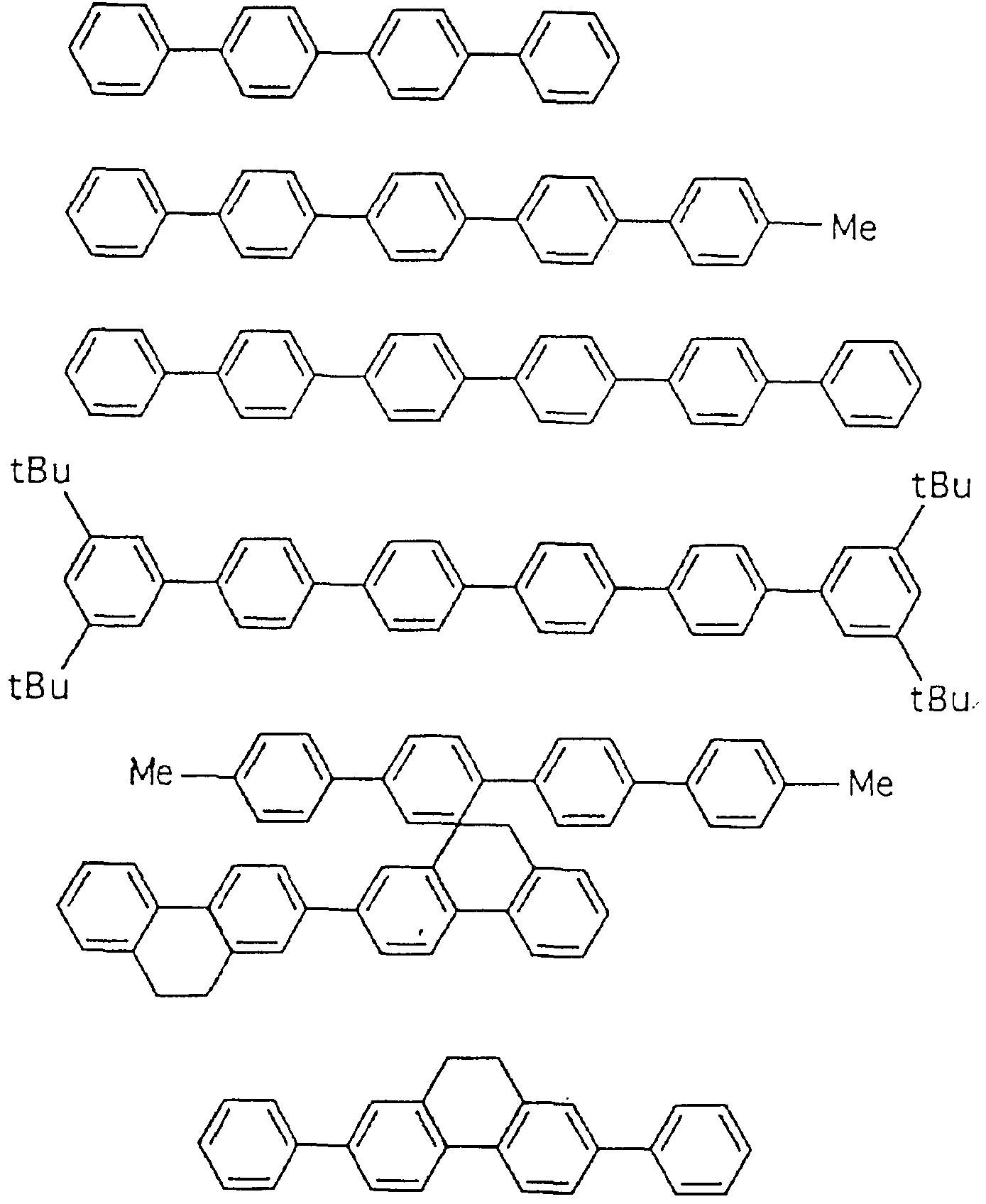


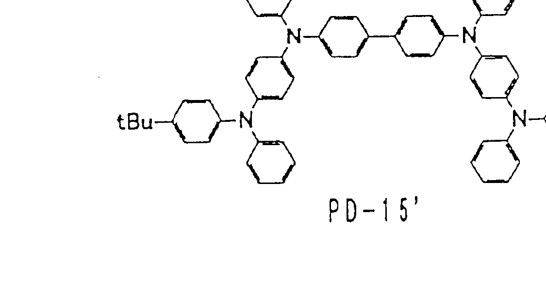


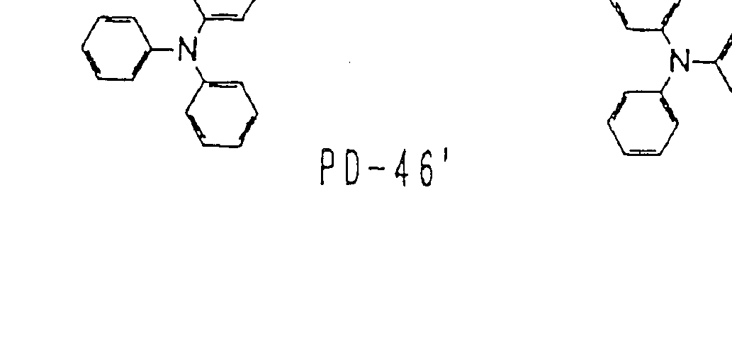


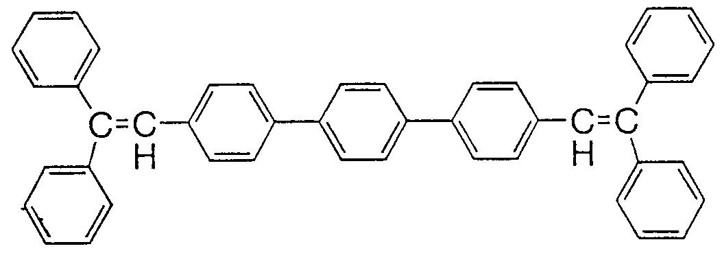
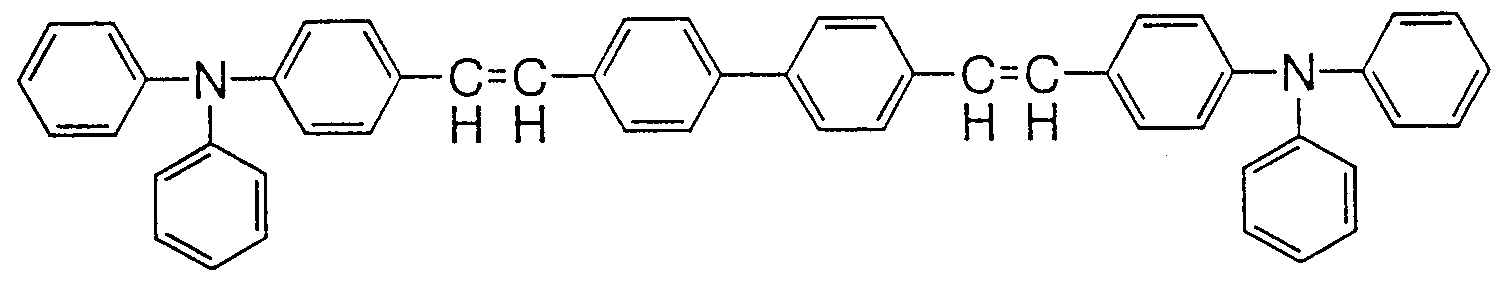


Claims


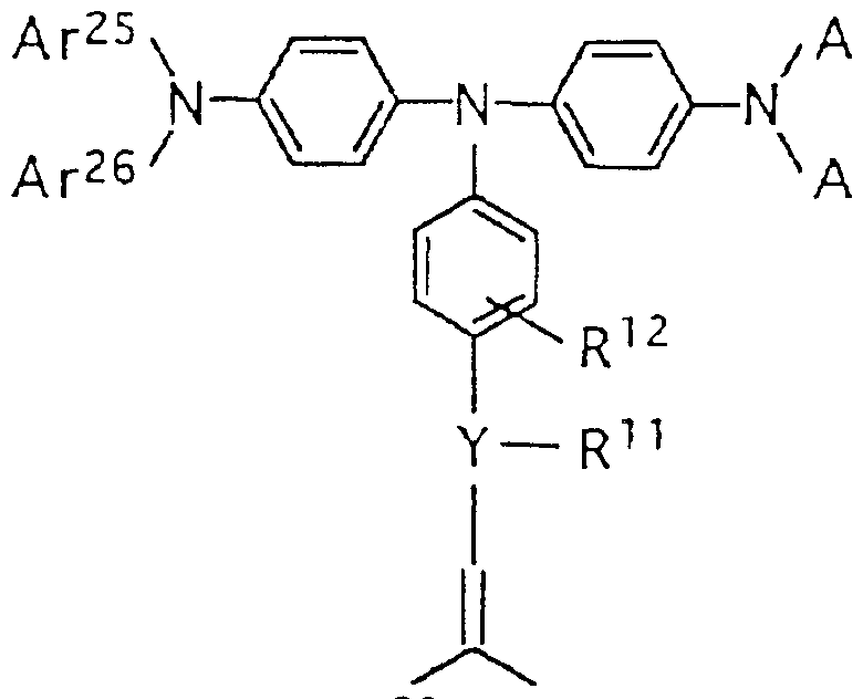
Priority Applications (5)
| Application Number | Priority Date | Filing Date | Title |
|---|---|---|---|
| US09/530,597 US6541129B1 (en) | 1998-09-09 | 1999-09-03 | Organic electroluminescence device and phenylenediamine derivative |
| EP99940653A EP1029909A4 (en) | 1998-09-09 | 1999-09-03 | Organic electroluminescence device and phenylenediamine derivative |
| KR1020007004003A KR100841842B1 (en) | 1998-09-09 | 1999-09-03 | Organic electroluminescence device and phenylenediamine derivative |
| US11/201,263 US7399537B2 (en) | 1998-09-09 | 2005-08-11 | Organic electroluminescence device and phenylenediamine derivative |
| US12/131,977 US20080241591A1 (en) | 1998-09-09 | 2008-06-03 | Organic electroluminescence device and phenylenediamine derivative |
Applications Claiming Priority (4)
| Application Number | Priority Date | Filing Date | Title |
|---|---|---|---|
| JP10/255563 | 1998-09-09 | ||
| JP25556398 | 1998-09-09 | ||
| JP4711099 | 1999-02-24 | ||
| JP11/47110 | 1999-02-24 |
Related Child Applications (3)
| Application Number | Title | Priority Date | Filing Date |
|---|---|---|---|
| US09/530,597 A-371-Of-International US6541129B1 (en) | 1998-09-09 | 1999-09-03 | Organic electroluminescence device and phenylenediamine derivative |
| US09530597 A-371-Of-International | 1999-09-03 | ||
| US10/331,645 Division US20030143430A1 (en) | 1998-09-09 | 2002-12-31 | Organic electroluminescence device and phenylenediamine derivative |
Publications (1)
| Publication Number | Publication Date |
|---|---|
| WO2000014174A1 true WO2000014174A1 (en) | 2000-03-16 |
Family
ID=26387261
Family Applications (1)
| Application Number | Title | Priority Date | Filing Date |
|---|---|---|---|
| PCT/JP1999/004794 WO2000014174A1 (en) | 1998-09-09 | 1999-09-03 | Organic electroluminescence device and phenylenediamine derivative |
Country Status (6)
| Country | Link |
|---|---|
| US (4) | US6541129B1 (en) |
| EP (1) | EP1029909A4 (en) |
| KR (3) | KR100805451B1 (en) |
| CN (1) | CN1213127C (en) |
| TW (2) | TWI222965B (en) |
| WO (1) | WO2000014174A1 (en) |
Cited By (9)
| Publication number | Priority date | Publication date | Assignee | Title |
|---|---|---|---|---|
| WO2004041774A1 (en) * | 2002-11-06 | 2004-05-21 | Idemitsu Kosan Co., Ltd. | Aromatic amine derivative and organic electroluminescent element employing the same |
| WO2006046441A1 (en) * | 2004-10-29 | 2006-05-04 | Idemitsu Kosan Co., Ltd. | Aromatic amine compound and organic electroluminescent device using same |
| WO2006057420A1 (en) * | 2004-11-26 | 2006-06-01 | Semiconductor Energy Laboratory Co., Ltd. | Light-emitting element, light-emitting device, and electronic device |
| JP2006179877A (en) * | 2004-11-26 | 2006-07-06 | Semiconductor Energy Lab Co Ltd | Light emitting element, light emitting device, and electronic device |
| WO2009107574A1 (en) * | 2008-02-25 | 2009-09-03 | 昭和電工株式会社 | Organic electroluminescent element, and manufacturing method and uses therefor |
| CN101180262B (en) * | 2005-04-18 | 2012-06-13 | 出光兴产株式会社 | aromatic triamine compound and organic electroluminescent element using the same |
| US8202630B2 (en) | 2004-11-05 | 2012-06-19 | Semiconductor Energy Laboratory Co., Ltd. | Light emitting element and light emitting device using the same |
| US9263681B2 (en) | 2012-12-10 | 2016-02-16 | Nitto Denko Corporation | Organic light emitting host materials |
| US9614162B2 (en) | 2012-12-17 | 2017-04-04 | Nitto Denko Corporation | Light-emitting devices comprising emissive layer |
Families Citing this family (168)
| Publication number | Priority date | Publication date | Assignee | Title |
|---|---|---|---|---|
| EP0891121B8 (en) * | 1996-12-28 | 2013-01-02 | Futaba Corporation | Organic electroluminescent elements |
| WO2000014174A1 (en) * | 1998-09-09 | 2000-03-16 | Idemitsu Kosan Co., Ltd. | Organic electroluminescence device and phenylenediamine derivative |
| EP1775335B9 (en) * | 1998-12-28 | 2013-06-26 | Idemitsu Kosan Co., Ltd. | Organic electroluminescent element |
| US6682832B2 (en) * | 1999-12-20 | 2004-01-27 | Matsushita Electric Industrial Co., Ltd. | Thin film el device |
| KR100721656B1 (en) | 2005-11-01 | 2007-05-23 | 주식회사 엘지화학 | Organic electronic devices |
| SG148030A1 (en) | 2000-12-28 | 2008-12-31 | Semiconductor Energy Lab | Luminescent device |
| TW518909B (en) * | 2001-01-17 | 2003-01-21 | Semiconductor Energy Lab | Luminescent device and method of manufacturing same |
| CN101397649B (en) | 2001-02-01 | 2011-12-28 | 株式会社半导体能源研究所 | Deposition device for manufacturing organic compound on substrate |
| CZ20032098A3 (en) * | 2001-02-02 | 2004-01-14 | Schering Corporation | 3,4-Disubstituted cyclobutene-1,2-diones and pharmaceutical composition containing thereof |
| GB0117377D0 (en) * | 2001-07-17 | 2001-09-05 | Opsys Ltd | "Tertiary diamines containing heterocyclic groups and their use in organic electroluminescent devices" |
| JP2003133071A (en) * | 2001-08-13 | 2003-05-09 | Victor Co Of Japan Ltd | Organic electroluminescent element and its manufacturing method |
| US6849345B2 (en) | 2001-09-28 | 2005-02-01 | Eastman Kodak Company | Organic electroluminescent devices with high luminance |
| US6610455B1 (en) | 2002-01-30 | 2003-08-26 | Eastman Kodak Company | Making electroluminscent display devices |
| US6872472B2 (en) | 2002-02-15 | 2005-03-29 | Eastman Kodak Company | Providing an organic electroluminescent device having stacked electroluminescent units |
| US6771021B2 (en) | 2002-05-28 | 2004-08-03 | Eastman Kodak Company | Lighting apparatus with flexible OLED area illumination light source and fixture |
| US6890627B2 (en) | 2002-08-02 | 2005-05-10 | Eastman Kodak Company | Laser thermal transfer from a donor element containing a hole-transporting layer |
| US6939660B2 (en) | 2002-08-02 | 2005-09-06 | Eastman Kodak Company | Laser thermal transfer donor including a separate dopant layer |
| US6747618B2 (en) | 2002-08-20 | 2004-06-08 | Eastman Kodak Company | Color organic light emitting diode display with improved lifetime |
| US6911961B2 (en) | 2002-10-11 | 2005-06-28 | Eastman Kodak Company | Method of designing an OLED display with lifetime optimized primaries |
| US7230594B2 (en) | 2002-12-16 | 2007-06-12 | Eastman Kodak Company | Color OLED display with improved power efficiency |
| CN1777592B (en) * | 2003-04-18 | 2011-09-07 | 株式会社半导体能源研究所 | Quinoxaline derivatives, and organic semiconductor devices, electroluminescent devices and electronic appliances, made by using the derivatives |
| CN1829702B (en) * | 2003-07-28 | 2010-11-17 | 株式会社半导体能源研究所 | Quinoxaline derivative and luminescent element comprising the same |
| US7221332B2 (en) | 2003-12-19 | 2007-05-22 | Eastman Kodak Company | 3D stereo OLED display |
| DE102004020046A1 (en) * | 2003-12-22 | 2005-07-28 | Sensient Imaging Technologies Gmbh | New tris(diarylaminoaryl)amine derivatives, used as hole transport substance or luminescent substance in organic electroluminescent or electrophotographic device, have triaryl-methyl- or -silyl-aryl substituent(s) |
| US8198801B2 (en) * | 2004-03-19 | 2012-06-12 | Lg Chem, Ltd. | Materials for injecting or transporting holes and organic electroluminescence devices using the same |
| US7541099B2 (en) * | 2004-05-21 | 2009-06-02 | Semiconductor Energy Laboratory Co., Ltd. | Anthracene derivative and light emitting element and light emitting device using the same |
| US7316756B2 (en) | 2004-07-27 | 2008-01-08 | Eastman Kodak Company | Desiccant for top-emitting OLED |
| US9040170B2 (en) | 2004-09-20 | 2015-05-26 | Global Oled Technology Llc | Electroluminescent device with quinazoline complex emitter |
| US7501152B2 (en) | 2004-09-21 | 2009-03-10 | Eastman Kodak Company | Delivering particulate material to a vaporization zone |
| US7501151B2 (en) | 2004-09-21 | 2009-03-10 | Eastman Kodak Company | Delivering particulate material to a vaporization zone |
| CN100573963C (en) | 2004-11-05 | 2009-12-23 | 株式会社半导体能源研究所 | Light-emitting component and its luminescent device of use |
| KR101251623B1 (en) * | 2004-11-30 | 2013-04-08 | 가부시키가이샤 한도오따이 에네루기 켄큐쇼 | Light emitting element and light emitting device |
| CN101906065B (en) * | 2004-12-28 | 2012-10-17 | 株式会社半导体能源研究所 | Anthracene derivative, light emitting element using the same, and light emitting device using the same |
| US7670506B1 (en) * | 2004-12-30 | 2010-03-02 | E. I. Du Pont De Nemours And Company | Photoactive compositions for liquid deposition |
| KR20070114713A (en) * | 2004-12-30 | 2007-12-04 | 이 아이 듀폰 디 네모아 앤드 캄파니 | Charge transport materials |
| EP1866983A4 (en) | 2005-02-28 | 2009-10-21 | Semiconductor Energy Lab | Composite material, light emitting element, light emitting device and electronic appliance using the composite material |
| KR100799223B1 (en) | 2005-03-04 | 2008-01-29 | 에스케이씨 주식회사 | Hole injecting material and organic electroluminescent device comprising same |
| US8057916B2 (en) | 2005-04-20 | 2011-11-15 | Global Oled Technology, Llc. | OLED device with improved performance |
| KR100739498B1 (en) * | 2005-05-07 | 2007-07-19 | 주식회사 두산 | Novel deuteriated aryl amine derivatives, preparation method thereof and organic light emitting diode using the same |
| CN2821911Y (en) * | 2005-06-30 | 2006-09-27 | 鸿富锦精密工业(深圳)有限公司 | General series bus connector |
| KR100696528B1 (en) * | 2005-07-22 | 2007-03-19 | 삼성에스디아이 주식회사 | Triarylamine-based compound, preparing method thereof and Organic luminescence display device using the same |
| EP1911079A4 (en) | 2005-07-25 | 2012-05-09 | Semiconductor Energy Lab | Light-emitting element, light-emitting device, and electronic appliance |
| WO2007020804A1 (en) * | 2005-08-12 | 2007-02-22 | Semiconductor Energy Laboratory Co., Ltd. | Arylamine compound and synthetic method thereof |
| KR101479924B1 (en) * | 2005-09-02 | 2015-01-12 | 가부시키가이샤 한도오따이 에네루기 켄큐쇼 | Anthracene derivative |
| KR20130121997A (en) | 2005-09-12 | 2013-11-06 | 가부시키가이샤 한도오따이 에네루기 켄큐쇼 | Quinoxaline derivative, and light emitting element, light emitting device, and electronic appliance using the same |
| US8956738B2 (en) | 2005-10-26 | 2015-02-17 | Global Oled Technology Llc | Organic element for low voltage electroluminescent devices |
| US9666826B2 (en) | 2005-11-30 | 2017-05-30 | Global Oled Technology Llc | Electroluminescent device including an anthracene derivative |
| US8920941B2 (en) * | 2005-12-28 | 2014-12-30 | Semiconductor Energy Laboratory Co., Ltd. | Pyrazine derivative, and light emitting element, display device, electronic device using the pyrazine derivative |
| CN101371619B (en) | 2006-01-18 | 2013-11-13 | Lg化学株式会社 | OLED having stacked organic light-emitting units |
| US7799439B2 (en) | 2006-01-25 | 2010-09-21 | Global Oled Technology Llc | Fluorocarbon electrode modification layer |
| EP2004616B1 (en) | 2006-03-21 | 2014-05-21 | Semiconductor Energy Laboratory Co., Ltd. | Quinoxaline derivative, and light-emitting element, light-emitting device, electronic device using the quinoxaline derivative |
| US9118020B2 (en) | 2006-04-27 | 2015-08-25 | Global Oled Technology Llc | Electroluminescent devices including organic eil layer |
| WO2007130047A1 (en) | 2006-05-08 | 2007-11-15 | Eastman Kodak Company | Oled electron-injecting layer |
| WO2007148660A1 (en) | 2006-06-22 | 2007-12-27 | Idemitsu Kosan Co., Ltd. | Organic electroluminescent device employing heterocycle-containing arylamine derivative |
| US8974918B2 (en) | 2006-07-04 | 2015-03-10 | Semiconductor Energy Laboratory Co., Ltd. | Display device and electronic device |
| GB2440368A (en) | 2006-07-26 | 2008-01-30 | Oled T Ltd | Cathode coating for an electroluminescent device |
| TW200816860A (en) * | 2006-09-22 | 2008-04-01 | Au Optronics Corp | Tandem organic electroluminescent elements and display using the same |
| KR101315379B1 (en) * | 2006-11-23 | 2013-10-10 | 삼성디스플레이 주식회사 | Manufacturing method of display device |
| DE102006059215A1 (en) | 2006-12-13 | 2008-07-10 | Sensient Imaging Technologies Gmbh | Arylamine-substituted divinylfluorenes and their use for electrophotographic applications and for OLEDS (Organic Light Emitting Devices) |
| GB0625540D0 (en) | 2006-12-22 | 2007-01-31 | Oled T Ltd | Electroluminescent devices |
| GB0625865D0 (en) | 2006-12-29 | 2007-02-07 | Oled T Ltd | Electro-optical or opto-electronic device |
| US8795855B2 (en) | 2007-01-30 | 2014-08-05 | Global Oled Technology Llc | OLEDs having high efficiency and excellent lifetime |
| US8178216B2 (en) * | 2007-02-28 | 2012-05-15 | Semiconductor Energy Laboratory Co., Ltd. | Quinoxaline derivative, and light-emitting element, light-emitting device, and electronic device including quinoxaline derivative |
| JP2008258272A (en) * | 2007-04-02 | 2008-10-23 | Fuji Xerox Co Ltd | Organic electroluminescent element, and display unit |
| US7911133B2 (en) | 2007-05-10 | 2011-03-22 | Global Oled Technology Llc | Electroluminescent device having improved light output |
| US8034465B2 (en) | 2007-06-20 | 2011-10-11 | Global Oled Technology Llc | Phosphorescent oled having double exciton-blocking layers |
| KR101407578B1 (en) * | 2007-07-24 | 2014-06-13 | 삼성디스플레이 주식회사 | Phenylphenoxazine or phenylphenothiazine based compounds and organic electroluminescence |
| US7812531B2 (en) | 2007-07-25 | 2010-10-12 | Global Oled Technology Llc | Preventing stress transfer in OLED display components |
| KR101625235B1 (en) | 2007-09-20 | 2016-05-27 | 바스프 에스이 | Electroluminescent device |
| US8129039B2 (en) | 2007-10-26 | 2012-03-06 | Global Oled Technology, Llc | Phosphorescent OLED device with certain fluoranthene host |
| US8420229B2 (en) | 2007-10-26 | 2013-04-16 | Global OLED Technologies LLC | OLED device with certain fluoranthene light-emitting dopants |
| US8431242B2 (en) | 2007-10-26 | 2013-04-30 | Global Oled Technology, Llc. | OLED device with certain fluoranthene host |
| US8076009B2 (en) | 2007-10-26 | 2011-12-13 | Global Oled Technology, Llc. | OLED device with fluoranthene electron transport materials |
| US8016631B2 (en) | 2007-11-16 | 2011-09-13 | Global Oled Technology Llc | Desiccant sealing arrangement for OLED devices |
| US8900722B2 (en) | 2007-11-29 | 2014-12-02 | Global Oled Technology Llc | OLED device employing alkali metal cluster compounds |
| JP5574598B2 (en) * | 2007-12-03 | 2014-08-20 | 株式会社半導体エネルギー研究所 | Quinoxaline derivative, and light-emitting element, light-emitting device, and electronic device using quinoxaline derivative |
| KR20140106740A (en) | 2007-12-03 | 2014-09-03 | 가부시키가이샤 한도오따이 에네루기 켄큐쇼 | Carbazole derivative, and light-emitting element, light-emitting device, and electronic device using carbazole derivative |
| US8877350B2 (en) | 2007-12-11 | 2014-11-04 | Global Oled Technology Llc | White OLED with two blue light-emitting layers |
| KR101563675B1 (en) | 2007-12-21 | 2015-10-27 | 가부시키가이샤 한도오따이 에네루기 켄큐쇼 | Triazole derivative, light-emitting element, light-emitting device, and electronic device |
| GB0804469D0 (en) | 2008-03-11 | 2008-04-16 | Oled T Ltd | Compounds having electroluminescent or electron transport properties |
| US7947974B2 (en) | 2008-03-25 | 2011-05-24 | Global Oled Technology Llc | OLED device with hole-transport and electron-transport materials |
| JP5611538B2 (en) * | 2008-05-16 | 2014-10-22 | 株式会社半導体エネルギー研究所 | Benzoxazole derivative, and light-emitting element, light-emitting device, lighting device, and electronic device using benzoxazole derivative |
| US8324800B2 (en) | 2008-06-12 | 2012-12-04 | Global Oled Technology Llc | Phosphorescent OLED device with mixed hosts |
| US8247088B2 (en) | 2008-08-28 | 2012-08-21 | Global Oled Technology Llc | Emitting complex for electroluminescent devices |
| JP5459903B2 (en) * | 2008-09-02 | 2014-04-02 | 株式会社半導体エネルギー研究所 | Anthracene derivative, light emitting element, light emitting device, electronic device, and lighting device |
| EP2161272A1 (en) | 2008-09-05 | 2010-03-10 | Basf Se | Phenanthrolines |
| US7931975B2 (en) | 2008-11-07 | 2011-04-26 | Global Oled Technology Llc | Electroluminescent device containing a flouranthene compound |
| US8088500B2 (en) | 2008-11-12 | 2012-01-03 | Global Oled Technology Llc | OLED device with fluoranthene electron injection materials |
| US7968215B2 (en) | 2008-12-09 | 2011-06-28 | Global Oled Technology Llc | OLED device with cyclobutene electron injection materials |
| US8216697B2 (en) | 2009-02-13 | 2012-07-10 | Global Oled Technology Llc | OLED with fluoranthene-macrocyclic materials |
| US8147989B2 (en) | 2009-02-27 | 2012-04-03 | Global Oled Technology Llc | OLED device with stabilized green light-emitting layer |
| US8102114B2 (en) | 2009-02-27 | 2012-01-24 | Global Oled Technology, Llc. | Method of manufacturing an inverted bottom-emitting OLED device |
| US8313845B2 (en) | 2009-03-31 | 2012-11-20 | Semiconductor Energy Laboratory Co., Ltd. | Quinoxaline derivative, and light-emitting element, light-emitting device, lighting device, and electronic device using quinoxaline derivative |
| US8283054B2 (en) | 2009-04-03 | 2012-10-09 | Global Oled Technology Llc | Tandem white OLED with efficient electron transfer |
| US8206842B2 (en) | 2009-04-06 | 2012-06-26 | Global Oled Technology Llc | Organic element for electroluminescent devices |
| EP2443213B1 (en) | 2009-06-18 | 2014-04-23 | Basf Se | Phenanthroazole compounds as hole transporting materials for electro luminescent devices |
| JP5778148B2 (en) | 2009-08-04 | 2015-09-16 | メルク パテント ゲーエムベーハー | Electronic devices containing polycyclic carbohydrates |
| KR101820974B1 (en) | 2009-09-16 | 2018-01-22 | 메르크 파텐트 게엠베하 | Formulations for the production of electronic devices |
| WO2011076323A1 (en) | 2009-12-22 | 2011-06-30 | Merck Patent Gmbh | Formulations comprising phase-separated functional materials |
| WO2011076326A1 (en) | 2009-12-22 | 2011-06-30 | Merck Patent Gmbh | Electroluminescent functional surfactants |
| WO2011076314A1 (en) | 2009-12-22 | 2011-06-30 | Merck Patent Gmbh | Electroluminescent formulations |
| WO2011110277A1 (en) | 2010-03-11 | 2011-09-15 | Merck Patent Gmbh | Fibers in therapy and cosmetics |
| KR101757016B1 (en) | 2010-03-11 | 2017-07-11 | 메르크 파텐트 게엠베하 | Radiative fibers |
| CN105949177B (en) | 2010-05-03 | 2019-02-01 | 默克专利有限公司 | Preparation and electronic device |
| WO2011147522A1 (en) | 2010-05-27 | 2011-12-01 | Merck Patent Gmbh | Compositions comprising quantum dots |
| US8586206B2 (en) * | 2010-06-30 | 2013-11-19 | Idemitsu Kosan Co., Ltd. | Aromatic amine derivative and organic electroluminescence device using the same |
| KR101720828B1 (en) | 2010-07-26 | 2017-03-28 | 메르크 파텐트 게엠베하 | Nanocrystals in devices |
| DE102010055901A1 (en) | 2010-12-23 | 2012-06-28 | Merck Patent Gmbh | Organic electroluminescent device |
| JP6351974B2 (en) | 2011-02-14 | 2018-07-04 | メルク パテント ゲーエムベーハー | Devices and methods for treatment of cells and cellular tissues |
| JP6356060B2 (en) | 2011-03-24 | 2018-07-11 | メルク パテント ゲーエムベーハー | Organic ionic functional materials |
| WO2012152366A1 (en) | 2011-05-12 | 2012-11-15 | Merck Patent Gmbh | Organic ionic compounds, compositions and electronic devices |
| KR20140036279A (en) | 2011-06-01 | 2014-03-25 | 메르크 파텐트 게엠베하 | Hybrid ambipolar tfts |
| EP2737553A1 (en) | 2011-07-25 | 2014-06-04 | Merck Patent GmbH | Copolymers with functionalized side chains |
| DE102011117422A1 (en) | 2011-10-28 | 2013-05-02 | Merck Patent Gmbh | Hyperbranched polymers, process for their preparation and their use in electronic devices |
| GB201306365D0 (en) | 2013-04-09 | 2013-05-22 | Kathirgamanathan Poopathy | Heterocyclic compounds and their use in electro-optical or opto-electronic devices |
| US10593886B2 (en) | 2013-08-25 | 2020-03-17 | Molecular Glasses, Inc. | OLED devices with improved lifetime using non-crystallizable molecular glass mixture hosts |
| KR102408597B1 (en) * | 2014-03-14 | 2022-06-14 | 닛산 가가쿠 가부시키가이샤 | Aniline derivative and use thereof |
| CN106687563B (en) | 2014-09-05 | 2023-03-14 | 默克专利有限公司 | Preparation and electronic device |
| WO2016107663A1 (en) | 2014-12-30 | 2016-07-07 | Merck Patent Gmbh | Formulations and electronic devices |
| KR102570137B1 (en) | 2015-03-30 | 2023-08-23 | 메르크 파텐트 게엠베하 | Formulation of an organic functional material comprising a siloxane solvent |
| KR101671277B1 (en) * | 2015-05-08 | 2016-11-01 | 머티어리얼사이언스 주식회사 | The method for manufacturing compound for organic electroluminescent device |
| WO2016198141A1 (en) | 2015-06-12 | 2016-12-15 | Merck Patent Gmbh | Esters containing non-aromatic cycles as solvents for oled formulations |
| US11046884B2 (en) | 2015-08-28 | 2021-06-29 | Merck Patent Gmbh | Formulation of an organic functional material comprising an epoxy group containing solvent |
| CN108368361A (en) | 2015-12-10 | 2018-08-03 | 默克专利有限公司 | Preparation containing the ketone comprising non-aromatic ring |
| US11171294B2 (en) | 2015-12-15 | 2021-11-09 | Merck Patent Gmbh | Esters containing aromatic groups as solvents for organic electronic formulations |
| EP3390549B1 (en) | 2015-12-16 | 2022-06-29 | Merck Patent GmbH | Formulations containing a solid solvent |
| KR20180095028A (en) | 2015-12-16 | 2018-08-24 | 메르크 파텐트 게엠베하 | A formulation containing a mixture of two or more different solvents |
| WO2017140404A1 (en) | 2016-02-17 | 2017-08-24 | Merck Patent Gmbh | Formulation of an organic functional material |
| DE102016003104A1 (en) | 2016-03-15 | 2017-09-21 | Merck Patent Gmbh | Container comprising a formulation containing at least one organic semiconductor |
| KR20170124957A (en) * | 2016-05-03 | 2017-11-13 | 롬엔드하스전자재료코리아유한회사 | Organic electroluminescent compound and organic electroluminescent device comprising the same |
| WO2017216129A1 (en) | 2016-06-16 | 2017-12-21 | Merck Patent Gmbh | Formulation of an organic functional material |
| JP2019523998A (en) | 2016-06-17 | 2019-08-29 | メルク パテント ゲーエムベーハー | Formulation of organic functional materials |
| TW201815998A (en) | 2016-06-28 | 2018-05-01 | 德商麥克專利有限公司 | Formulation of an organic functional material |
| JP6980757B2 (en) | 2016-08-04 | 2021-12-15 | メルク パテント ゲーエムベーハー | Formulation of organic functional materials |
| US11538992B2 (en) | 2016-10-31 | 2022-12-27 | Merck Patent Gmbh | Formulation of an organic functional material |
| WO2018077662A1 (en) | 2016-10-31 | 2018-05-03 | Merck Patent Gmbh | Formulation of an organic functional material |
| CN110036498B (en) | 2016-12-06 | 2023-04-18 | 默克专利有限公司 | Method for manufacturing electronic device |
| CN110168047B (en) | 2016-12-13 | 2023-08-08 | 默克专利有限公司 | Preparation of organic functional material |
| TW201835300A (en) | 2016-12-22 | 2018-10-01 | 德商麥克專利有限公司 | Mixtures comprising at least two organic-functional compounds |
| TWI791481B (en) | 2017-01-30 | 2023-02-11 | 德商麥克專利有限公司 | Method for forming an organic electroluminescence (el) element |
| TWI763772B (en) | 2017-01-30 | 2022-05-11 | 德商麥克專利有限公司 | Method for forming an organic element of an electronic device |
| KR20190131554A (en) | 2017-03-31 | 2019-11-26 | 메르크 파텐트 게엠베하 | Printing method for organic light emitting diodes (OLED) |
| CN110494514A (en) | 2017-04-10 | 2019-11-22 | 默克专利有限公司 | The preparation of organic functional material |
| JP7330898B2 (en) | 2017-05-03 | 2023-08-22 | メルク パテント ゲーエムベーハー | Formulation of organic functional material |
| KR20200030573A (en) | 2017-07-18 | 2020-03-20 | 메르크 파텐트 게엠베하 | Formulation of organic functional materials |
| KR20200093653A (en) | 2017-12-15 | 2020-08-05 | 메르크 파텐트 게엠베하 | Formulation of organic functional materials |
| EP3518303B1 (en) | 2018-01-26 | 2021-10-06 | Samsung Display Co., Ltd. | N-(4-(8-(phenyl)naphthalen-2-yl)phenyl)-n,n'-di(phenyl)-amine derivatives and related compounds for use in organic electroluminescence devices |
| JP7465062B2 (en) | 2018-01-26 | 2024-04-10 | 三星ディスプレイ株式會社 | Organic electroluminescent device and monoamine compound for organic electroluminescent device |
| WO2019162483A1 (en) | 2018-02-26 | 2019-08-29 | Merck Patent Gmbh | Formulation of an organic functional material |
| KR102508497B1 (en) | 2018-03-26 | 2023-03-10 | 삼성디스플레이 주식회사 | Heterocyclic compound and organic light emitting device comprising the same |
| JP7379389B2 (en) | 2018-06-15 | 2023-11-14 | メルク パテント ゲーエムベーハー | Formulations of organic functional materials |
| KR102628848B1 (en) | 2018-08-10 | 2024-01-25 | 삼성디스플레이 주식회사 | Condensed compound and organic light-emitting device including the same |
| CN112740432A (en) | 2018-09-24 | 2021-04-30 | 默克专利有限公司 | Method for producing granular material |
| EP3878022A1 (en) | 2018-11-06 | 2021-09-15 | Merck Patent GmbH | Method for forming an organic element of an electronic device |
| US11043639B2 (en) | 2018-12-28 | 2021-06-22 | Samsung Electronics Co., Ltd. | Charge transport material, composition including the charge transport material, and organic light-emitting device including the composition |
| KR20200099249A (en) | 2019-02-13 | 2020-08-24 | 삼성디스플레이 주식회사 | Organic light emitting device |
| KR20200113057A (en) | 2019-03-20 | 2020-10-06 | 삼성디스플레이 주식회사 | AMINE-BASED compound and organic light emitting device comprising the same |
| KR20210038736A (en) | 2019-09-27 | 2021-04-08 | 삼성디스플레이 주식회사 | Condensed-cyclic compound and organic light emitting device including the same |
| CN111205237B (en) * | 2020-01-13 | 2020-12-29 | 长春海谱润斯科技股份有限公司 | Triamine derivative and organic electroluminescent device thereof |
| CN115700058A (en) | 2020-04-21 | 2023-02-03 | 默克专利有限公司 | Emulsions comprising organic functional materials |
| WO2021259824A1 (en) | 2020-06-23 | 2021-12-30 | Merck Patent Gmbh | Method for producing a mixture |
| EP3950661A1 (en) * | 2020-08-03 | 2022-02-09 | Ecole Polytechnique Fédérale de Lausanne (EPFL) | Hole transport material, synthesis thereof, and solar cell |
| KR20230114756A (en) | 2020-12-08 | 2023-08-01 | 메르크 파텐트 게엠베하 | Ink Systems and Methods for Inkjet Printing |
| EP4340969A1 (en) | 2021-05-21 | 2024-03-27 | Merck Patent GmbH | Method for the continuous purification of at least one functional material and device for the continuous purification of at least one functional material |
| KR20240045247A (en) | 2021-08-02 | 2024-04-05 | 메르크 파텐트 게엠베하 | Printing method by combining inks |
| WO2023031073A1 (en) | 2021-08-31 | 2023-03-09 | Merck Patent Gmbh | Composition |
| TW202349760A (en) | 2021-10-05 | 2023-12-16 | 德商麥克專利有限公司 | Method for forming an organic element of an electronic device |
| WO2023237458A1 (en) | 2022-06-07 | 2023-12-14 | Merck Patent Gmbh | Method of printing a functional layer of an electronic device by combining inks |
Citations (9)
| Publication number | Priority date | Publication date | Assignee | Title |
|---|---|---|---|---|
| JPS62267749A (en) * | 1986-05-16 | 1987-11-20 | Fuji Xerox Co Ltd | Novel benzidine compound and its production |
| JPH0394262A (en) * | 1989-09-06 | 1991-04-19 | Konica Corp | Electrophotographic sensitive body |
| JPH0820771A (en) * | 1994-07-08 | 1996-01-23 | Toyo Ink Mfg Co Ltd | Hole-transporting material and its use |
| WO1996022273A1 (en) * | 1995-01-19 | 1996-07-25 | Idemitsu Kosan Co., Ltd. | Organic electroluminescent element, organic thin film, and triamine compounds |
| JPH08259934A (en) * | 1995-03-20 | 1996-10-08 | Matsushita Electric Ind Co Ltd | Electroluminescent element |
| JPH09301934A (en) * | 1996-05-10 | 1997-11-25 | Kemipuro Kasei Kk | High molecular weight aromatic amine compound and hole-transporting material |
| WO1998030071A1 (en) * | 1996-12-28 | 1998-07-09 | Tdk Corporation | Organic electroluminescent elements |
| JPH1154280A (en) * | 1997-07-31 | 1999-02-26 | Chisso Corp | Organic electroluminescent element using naphthylamine derivative |
| JPH11167992A (en) * | 1997-12-05 | 1999-06-22 | Mitsui Chem Inc | Organic electroluminescent element |
Family Cites Families (14)
| Publication number | Priority date | Publication date | Assignee | Title |
|---|---|---|---|---|
| CA2037917A1 (en) * | 1989-08-18 | 1991-02-19 | Chishio Hosokawa | Organic electroluminescence device |
| JP3016896B2 (en) * | 1991-04-08 | 2000-03-06 | パイオニア株式会社 | Organic electroluminescence device |
| WO1994006157A1 (en) * | 1992-08-28 | 1994-03-17 | Idemitsu Kosan Co., Ltd. | Charge injection assistant and organic electroluminescence device containing the same |
| DE69432686T2 (en) * | 1993-09-29 | 2004-03-18 | Idemitsu Kosan Co. Ltd. | Acrylenediamine derivatives and organic electroluminescent element containing them |
| JPH09222741A (en) * | 1995-12-11 | 1997-08-26 | Toyo Ink Mfg Co Ltd | Positive hole transferring material and its use |
| DE69739752D1 (en) * | 1996-08-19 | 2010-03-18 | Tdk Corp | Organic electroluminescent device |
| JP3525034B2 (en) * | 1997-07-31 | 2004-05-10 | 出光興産株式会社 | Organic electroluminescence device |
| US5853905A (en) * | 1997-09-08 | 1998-12-29 | Motorola, Inc. | Efficient single layer electroluminescent device |
| US5853906A (en) * | 1997-10-14 | 1998-12-29 | Xerox Corporation | Conductive polymer compositions and processes thereof |
| KR100582328B1 (en) * | 1998-04-09 | 2006-05-23 | 이데미쓰 고산 가부시키가이샤 | Organic electroluminescent device |
| TW521537B (en) * | 1998-05-08 | 2003-02-21 | Idemitsu Kosan Co | Organic electroluminescence element |
| WO2000014174A1 (en) * | 1998-09-09 | 2000-03-16 | Idemitsu Kosan Co., Ltd. | Organic electroluminescence device and phenylenediamine derivative |
| KR100702763B1 (en) * | 1999-02-15 | 2007-04-03 | 이데미쓰 고산 가부시키가이샤 | Organic electroluminescent device and method of manufacture thereof |
| JP3895178B2 (en) * | 1999-09-30 | 2007-03-22 | 出光興産株式会社 | Amine compound and organic electroluminescence device using the same |
-
1999
- 1999-09-03 WO PCT/JP1999/004794 patent/WO2000014174A1/en active Application Filing
- 1999-09-03 KR KR1020067012880A patent/KR100805451B1/en not_active IP Right Cessation
- 1999-09-03 CN CNB998015229A patent/CN1213127C/en not_active Expired - Lifetime
- 1999-09-03 KR KR1020007004003A patent/KR100841842B1/en active IP Right Grant
- 1999-09-03 KR KR1020077012605A patent/KR100837029B1/en active IP Right Grant
- 1999-09-03 US US09/530,597 patent/US6541129B1/en not_active Expired - Lifetime
- 1999-09-03 EP EP99940653A patent/EP1029909A4/en not_active Withdrawn
- 1999-09-08 TW TW088115517A patent/TWI222965B/en not_active IP Right Cessation
- 1999-09-08 TW TW091117339A patent/TWI261583B/en not_active IP Right Cessation
-
2002
- 2002-12-31 US US10/331,645 patent/US20030143430A1/en active Pending
-
2005
- 2005-08-11 US US11/201,263 patent/US7399537B2/en not_active Expired - Fee Related
-
2008
- 2008-06-03 US US12/131,977 patent/US20080241591A1/en not_active Abandoned
Patent Citations (9)
| Publication number | Priority date | Publication date | Assignee | Title |
|---|---|---|---|---|
| JPS62267749A (en) * | 1986-05-16 | 1987-11-20 | Fuji Xerox Co Ltd | Novel benzidine compound and its production |
| JPH0394262A (en) * | 1989-09-06 | 1991-04-19 | Konica Corp | Electrophotographic sensitive body |
| JPH0820771A (en) * | 1994-07-08 | 1996-01-23 | Toyo Ink Mfg Co Ltd | Hole-transporting material and its use |
| WO1996022273A1 (en) * | 1995-01-19 | 1996-07-25 | Idemitsu Kosan Co., Ltd. | Organic electroluminescent element, organic thin film, and triamine compounds |
| JPH08259934A (en) * | 1995-03-20 | 1996-10-08 | Matsushita Electric Ind Co Ltd | Electroluminescent element |
| JPH09301934A (en) * | 1996-05-10 | 1997-11-25 | Kemipuro Kasei Kk | High molecular weight aromatic amine compound and hole-transporting material |
| WO1998030071A1 (en) * | 1996-12-28 | 1998-07-09 | Tdk Corporation | Organic electroluminescent elements |
| JPH1154280A (en) * | 1997-07-31 | 1999-02-26 | Chisso Corp | Organic electroluminescent element using naphthylamine derivative |
| JPH11167992A (en) * | 1997-12-05 | 1999-06-22 | Mitsui Chem Inc | Organic electroluminescent element |
Non-Patent Citations (1)
| Title |
|---|
| See also references of EP1029909A4 * |
Cited By (11)
| Publication number | Priority date | Publication date | Assignee | Title |
|---|---|---|---|---|
| WO2004041774A1 (en) * | 2002-11-06 | 2004-05-21 | Idemitsu Kosan Co., Ltd. | Aromatic amine derivative and organic electroluminescent element employing the same |
| WO2006046441A1 (en) * | 2004-10-29 | 2006-05-04 | Idemitsu Kosan Co., Ltd. | Aromatic amine compound and organic electroluminescent device using same |
| US8202630B2 (en) | 2004-11-05 | 2012-06-19 | Semiconductor Energy Laboratory Co., Ltd. | Light emitting element and light emitting device using the same |
| US8455114B2 (en) | 2004-11-05 | 2013-06-04 | Semiconductor Energy Laboratory Co., Ltd. | Light emitting element and light emitting device using the same |
| WO2006057420A1 (en) * | 2004-11-26 | 2006-06-01 | Semiconductor Energy Laboratory Co., Ltd. | Light-emitting element, light-emitting device, and electronic device |
| JP2006179877A (en) * | 2004-11-26 | 2006-07-06 | Semiconductor Energy Lab Co Ltd | Light emitting element, light emitting device, and electronic device |
| US7646010B2 (en) | 2004-11-26 | 2010-01-12 | Semiconductor Energy Laboratory Co., Ltd. | Light-emitting element, light-emitting device, and electronic device |
| CN101180262B (en) * | 2005-04-18 | 2012-06-13 | 出光兴产株式会社 | aromatic triamine compound and organic electroluminescent element using the same |
| WO2009107574A1 (en) * | 2008-02-25 | 2009-09-03 | 昭和電工株式会社 | Organic electroluminescent element, and manufacturing method and uses therefor |
| US9263681B2 (en) | 2012-12-10 | 2016-02-16 | Nitto Denko Corporation | Organic light emitting host materials |
| US9614162B2 (en) | 2012-12-17 | 2017-04-04 | Nitto Denko Corporation | Light-emitting devices comprising emissive layer |
Also Published As
| Publication number | Publication date |
|---|---|
| US20060082294A1 (en) | 2006-04-20 |
| KR20070073966A (en) | 2007-07-10 |
| US7399537B2 (en) | 2008-07-15 |
| CN1277626A (en) | 2000-12-20 |
| EP1029909A1 (en) | 2000-08-23 |
| KR100837029B1 (en) | 2008-06-10 |
| KR100805451B1 (en) | 2008-02-20 |
| KR100841842B1 (en) | 2008-06-27 |
| KR20060085255A (en) | 2006-07-26 |
| EP1029909A4 (en) | 2007-01-10 |
| KR20010031112A (en) | 2001-04-16 |
| US20030143430A1 (en) | 2003-07-31 |
| TWI222965B (en) | 2004-11-01 |
| US6541129B1 (en) | 2003-04-01 |
| US20080241591A1 (en) | 2008-10-02 |
| CN1213127C (en) | 2005-08-03 |
| TWI261583B (en) | 2006-09-11 |
Similar Documents
| Publication | Publication Date | Title |
|---|---|---|
| WO2000014174A1 (en) | Organic electroluminescence device and phenylenediamine derivative | |
| JP4542646B2 (en) | Organic electroluminescence device and phenylenediamine derivative | |
| KR100843819B1 (en) | Anthracene derivatives and organic electroluminescent devices made by using the same | |
| TWI429650B (en) | Organic electroluminescent elements | |
| JP3109896B2 (en) | Organic electroluminescence device | |
| JP4211869B2 (en) | Diaminoarylene compound having carbazolyl group and use thereof | |
| JP4765589B2 (en) | Fluorene compound having carbazolyl group and use thereof | |
| JP5255296B2 (en) | Materials and compounds for organic electroluminescence devices | |
| JPH08239655A (en) | Organic electroluminescence element | |
| JP2003040873A (en) | New quinoxaline derivative and organic electroluminescent element utilizing the same | |
| WO2007043484A1 (en) | Carbazole-containing amine compound and use thereof | |
| JP2009194042A (en) | Charge transporting material for use of organic electroluminescence element containing carbazolyl group and its use | |
| JP2007109988A (en) | Organic electroluminescence element | |
| JPH0688072A (en) | Organic electroluminescent element | |
| JPH09241629A (en) | Organic electroluminescent element | |
| JP2010126571A (en) | Organic electroluminescent element material and organic electroluminescent element | |
| JP4224252B2 (en) | Compound for organic EL element, organic EL element | |
| JP2007126439A (en) | Carbazole-containing amine compound and use thereof | |
| JP2009221442A (en) | Material for organic electroluminescent element and organic electroluminescent element | |
| JPH08333569A (en) | Organic electroluminescence element | |
| JP5277578B2 (en) | Compound having carbazolyl group and use thereof | |
| JP2003238501A (en) | Aromatic oligoamine derivative and organic electroluminescent element containing the same | |
| JP4112719B2 (en) | Aromatic hydrocarbon compound and organic electroluminescence device using the same | |
| JP2000191560A (en) | Aromatic hydrocarbon compound and organic electroluminescence element using thereof | |
| JP4802645B2 (en) | Materials for organic electroluminescence devices |
Legal Events
| Date | Code | Title | Description |
|---|---|---|---|
| WWE | Wipo information: entry into national phase |
Ref document number: 99801522.9 Country of ref document: CN |
|
| AK | Designated states |
Kind code of ref document: A1 Designated state(s): CN KR US |
|
| AL | Designated countries for regional patents |
Kind code of ref document: A1 Designated state(s): AT BE CH CY DE DK ES FI FR GB GR IE IT LU MC NL PT SE |
|
| WWE | Wipo information: entry into national phase |
Ref document number: 1999940653 Country of ref document: EP |
|
| WWE | Wipo information: entry into national phase |
Ref document number: 1020007004003 Country of ref document: KR |
|
| WWE | Wipo information: entry into national phase |
Ref document number: 09530597 Country of ref document: US |
|
| 121 | Ep: the epo has been informed by wipo that ep was designated in this application | ||
| WWP | Wipo information: published in national office |
Ref document number: 1999940653 Country of ref document: EP |
|
| WWP | Wipo information: published in national office |
Ref document number: 1020007004003 Country of ref document: KR |