UST106201I4 - Master image chip organization technique or method - Google Patents
Master image chip organization technique or method Download PDFInfo
- Publication number
- UST106201I4 UST106201I4 US06/457,786 US45778683A UST106201I4 US T106201 I4 UST106201 I4 US T106201I4 US 45778683 A US45778683 A US 45778683A US T106201 I4 UST106201 I4 US T106201I4
- Authority
- US
- United States
- Prior art keywords
- pattern
- conductors
- spacing
- coordinate system
- macro
- Prior art date
- Legal status (The legal status is an assumption and is not a legal conclusion. Google has not performed a legal analysis and makes no representation as to the accuracy of the status listed.)
- Pending
Links
Images


Classifications
-
- H—ELECTRICITY
- H10—SEMICONDUCTOR DEVICES; ELECTRIC SOLID-STATE DEVICES NOT OTHERWISE PROVIDED FOR
- H10W—GENERIC PACKAGES, INTERCONNECTIONS, CONNECTORS OR OTHER CONSTRUCTIONAL DETAILS OF DEVICES COVERED BY CLASS H10
- H10W20/00—Interconnections in chips, wafers or substrates
- H10W20/40—Interconnections external to wafers or substrates, e.g. back-end-of-line [BEOL] metallisations or vias connecting to gate electrodes
- H10W20/41—Interconnections external to wafers or substrates, e.g. back-end-of-line [BEOL] metallisations or vias connecting to gate electrodes characterised by their conductive parts
- H10W20/43—Layouts of interconnections
-
- H—ELECTRICITY
- H10—SEMICONDUCTOR DEVICES; ELECTRIC SOLID-STATE DEVICES NOT OTHERWISE PROVIDED FOR
- H10D—INORGANIC ELECTRIC SEMICONDUCTOR DEVICES
- H10D84/00—Integrated devices formed in or on semiconductor substrates that comprise only semiconducting layers, e.g. on Si wafers or on GaAs-on-Si wafers
- H10D84/90—Masterslice integrated circuits
- H10D84/901—Masterslice integrated circuits comprising bipolar technology
Landscapes
- Internal Circuitry In Semiconductor Integrated Circuit Devices (AREA)
Abstract
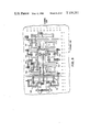
A method for forming an improved integrated circuit chip structure having a surface from which regions of different conductivity type are arranged in a plurality of electrically isolated macro circuits, each macro circuit including interconnected components, a first X pattern of equally spaced parallel conductors overlying and electrically insulated from said chip structure surface, said first X pattern of conductors being selectively connected to at least certain ones of said plurality of macro circuits, a second Y pattern of equally spaced parallel conductors overlying and electrically insulated from said first pattern of parallel conductors, said second Y pattern of conductors being selectively connected to at least selected certain ones of said first pattern of electrical conductors, said spacing one from another of said first X pattern of conductors being equal to said spacing one from another of said second Y pattern of conductors, said first pattern of conductors being orthogonal of said second pattern of conductors, and each of said connections occurring exclusively at points in space corresponding to X-Y intersections of an X-Y coordinate system, where said X-Y coordinate system geometrically corresponds identically to said X-Y pattern of conductors.
Priority Applications (1)
| Application Number | Priority Date | Filing Date | Title |
|---|---|---|---|
| US06/457,786 UST106201I4 (en) | 1978-12-29 | 1983-01-13 | Master image chip organization technique or method |
Applications Claiming Priority (2)
| Application Number | Priority Date | Filing Date | Title |
|---|---|---|---|
| US05/974,576 US4295149A (en) | 1978-12-29 | 1978-12-29 | Master image chip organization technique or method |
| US06/457,786 UST106201I4 (en) | 1978-12-29 | 1983-01-13 | Master image chip organization technique or method |
Related Parent Applications (1)
| Application Number | Title | Priority Date | Filing Date |
|---|---|---|---|
| US06224240 Continuation | 1981-01-12 |
Publications (1)
| Publication Number | Publication Date |
|---|---|
| UST106201I4 true UST106201I4 (en) | 1986-03-04 |
Family
ID=27038728
Family Applications (1)
| Application Number | Title | Priority Date | Filing Date |
|---|---|---|---|
| US06/457,786 Pending UST106201I4 (en) | 1978-12-29 | 1983-01-13 | Master image chip organization technique or method |
Country Status (1)
| Country | Link |
|---|---|
| US (1) | UST106201I4 (en) |
Cited By (1)
| Publication number | Priority date | Publication date | Assignee | Title |
|---|---|---|---|---|
| US20020134104A1 (en) * | 2000-11-10 | 2002-09-26 | James Stenhouse | High efficiency discontinuous cryogenic mixed gas refrigeration system using coalescent (depth) membrane filters and plate heat exchangers and refrigerant therefore |
-
1983
- 1983-01-13 US US06/457,786 patent/UST106201I4/en active Pending
Cited By (1)
| Publication number | Priority date | Publication date | Assignee | Title |
|---|---|---|---|---|
| US20020134104A1 (en) * | 2000-11-10 | 2002-09-26 | James Stenhouse | High efficiency discontinuous cryogenic mixed gas refrigeration system using coalescent (depth) membrane filters and plate heat exchangers and refrigerant therefore |
Similar Documents
| Publication | Publication Date | Title |
|---|---|---|
| EP0070861B1 (en) | Wafer and method of testing networks thereon | |
| US2889532A (en) | Wiring assembly with stacked conductor cards | |
| US4458297A (en) | Universal interconnection substrate | |
| US3670208A (en) | Microelectronic package, buss strip and printed circuit base assembly | |
| GB1443361A (en) | Lsi chip construction | |
| KR890001179A (en) | Semiconductor integrated circuit with multilayer power lines | |
| US4513307A (en) | CMOS/SOS transistor gate array apparatus | |
| EP0238314A3 (en) | Computer-aided automatic wiring method for semiconductor integrated circuit device | |
| GB1276095A (en) | Microcircuits and processes for their manufacture | |
| GB987296A (en) | Improvements in or relating to a multilayer circuitry | |
| JP2513443B2 (en) | Multilayer circuit board assembly | |
| US5077451A (en) | Custom tooled printed circuit board | |
| GB1187619A (en) | Improvements relating to Electrical Interconnection Grids | |
| GB1513893A (en) | Integrated circuit structure | |
| US4295182A (en) | Interconnection arrangements for testing microelectronic circuit chips on a wafer | |
| UST106201I4 (en) | Master image chip organization technique or method | |
| US3644937A (en) | Channel-stacking input/output interconnections | |
| EP0021661B1 (en) | Semiconductor master-slice device | |
| EP0069762B1 (en) | Universal interconnection substrate | |
| US4361634A (en) | Artwork master for production of multilayer circuit board | |
| US3217208A (en) | Utility printed circuit board | |
| IT1162549B (en) | DIELECTRIC STRUCTURE IN MULTIPLE LAYERS FOR THE INSTALLATION OF INTEGRATED CIRCUITS | |
| EP0338817A3 (en) | Semiconductor integrated circuit device and method of producing the same using master slice approach | |
| JPS6095940A (en) | Multiplex passage signal distributing system | |
| GB1561567A (en) | Printed circuit board |
Legal Events
| Date | Code | Title | Description |
|---|---|---|---|
| STPP | Information on status: patent application and granting procedure in general |
Free format text: DEFENSIVE PUBLICATION OR SIR FILE |