US9995986B2 - Light control element, light control device, and method for producing light control element - Google Patents
Light control element, light control device, and method for producing light control element Download PDFInfo
- Publication number
- US9995986B2 US9995986B2 US15/406,048 US201715406048A US9995986B2 US 9995986 B2 US9995986 B2 US 9995986B2 US 201715406048 A US201715406048 A US 201715406048A US 9995986 B2 US9995986 B2 US 9995986B2
- Authority
- US
- United States
- Prior art keywords
- layer
- light control
- control element
- electrolyte layer
- organic electrolyte
- Prior art date
- Legal status (The legal status is an assumption and is not a legal conclusion. Google has not performed a legal analysis and makes no representation as to the accuracy of the status listed.)
- Active
Links
- 238000004519 manufacturing process Methods 0.000 title claims description 32
- 239000005486 organic electrolyte Substances 0.000 claims abstract description 50
- 239000003792 electrolyte Substances 0.000 claims abstract description 48
- 238000009825 accumulation Methods 0.000 claims abstract description 47
- 239000003054 catalyst Substances 0.000 claims abstract description 39
- BPUBBGLMJRNUCC-UHFFFAOYSA-N oxygen(2-);tantalum(5+) Chemical group [O-2].[O-2].[O-2].[O-2].[O-2].[Ta+5].[Ta+5] BPUBBGLMJRNUCC-UHFFFAOYSA-N 0.000 claims description 25
- 239000000463 material Substances 0.000 claims description 21
- 238000000034 method Methods 0.000 claims description 17
- 230000005540 biological transmission Effects 0.000 claims description 15
- 229910001936 tantalum oxide Inorganic materials 0.000 claims description 12
- PBCFLUZVCVVTBY-UHFFFAOYSA-N tantalum pentoxide Inorganic materials O=[Ta](=O)O[Ta](=O)=O PBCFLUZVCVVTBY-UHFFFAOYSA-N 0.000 claims description 10
- 239000000758 substrate Substances 0.000 claims description 9
- 230000007704 transition Effects 0.000 claims description 8
- 239000004696 Poly ether ether ketone Substances 0.000 claims description 7
- 238000010030 laminating Methods 0.000 claims description 7
- 229920002530 polyetherether ketone Polymers 0.000 claims description 7
- 238000004544 sputter deposition Methods 0.000 claims description 7
- 229920000557 Nafion® Polymers 0.000 claims description 6
- 238000003980 solgel method Methods 0.000 claims description 5
- 238000004528 spin coating Methods 0.000 claims description 5
- 239000010410 layer Substances 0.000 description 235
- KDLHZDBZIXYQEI-UHFFFAOYSA-N Palladium Chemical group [Pd] KDLHZDBZIXYQEI-UHFFFAOYSA-N 0.000 description 37
- 238000002484 cyclic voltammetry Methods 0.000 description 23
- 230000000052 comparative effect Effects 0.000 description 22
- 239000010408 film Substances 0.000 description 18
- 229910052763 palladium Inorganic materials 0.000 description 18
- 239000011241 protective layer Substances 0.000 description 18
- 238000003487 electrochemical reaction Methods 0.000 description 12
- QGLKJKCYBOYXKC-UHFFFAOYSA-N nonaoxidotritungsten Chemical compound O=[W]1(=O)O[W](=O)(=O)O[W](=O)(=O)O1 QGLKJKCYBOYXKC-UHFFFAOYSA-N 0.000 description 10
- 229910001930 tungsten oxide Inorganic materials 0.000 description 10
- 230000002950 deficient Effects 0.000 description 9
- 230000007423 decrease Effects 0.000 description 8
- 238000007733 ion plating Methods 0.000 description 8
- 229910000861 Mg alloy Inorganic materials 0.000 description 6
- PXHVJJICTQNCMI-UHFFFAOYSA-N Nickel Chemical compound [Ni] PXHVJJICTQNCMI-UHFFFAOYSA-N 0.000 description 6
- 229910052782 aluminium Inorganic materials 0.000 description 6
- XAGFODPZIPBFFR-UHFFFAOYSA-N aluminium Chemical compound [Al] XAGFODPZIPBFFR-UHFFFAOYSA-N 0.000 description 6
- XOLBLPGZBRYERU-UHFFFAOYSA-N tin dioxide Chemical compound O=[Sn]=O XOLBLPGZBRYERU-UHFFFAOYSA-N 0.000 description 6
- 238000000576 coating method Methods 0.000 description 5
- 238000010586 diagram Methods 0.000 description 5
- -1 hydrogen ions Chemical class 0.000 description 5
- 238000005259 measurement Methods 0.000 description 5
- BASFCYQUMIYNBI-UHFFFAOYSA-N platinum Chemical compound [Pt] BASFCYQUMIYNBI-UHFFFAOYSA-N 0.000 description 5
- 238000002847 impedance measurement Methods 0.000 description 4
- 239000010409 thin film Substances 0.000 description 4
- 229910000882 Ca alloy Inorganic materials 0.000 description 3
- OYPRJOBELJOOCE-UHFFFAOYSA-N Calcium Chemical compound [Ca] OYPRJOBELJOOCE-UHFFFAOYSA-N 0.000 description 3
- 229910000990 Ni alloy Inorganic materials 0.000 description 3
- 239000011575 calcium Substances 0.000 description 3
- 238000009792 diffusion process Methods 0.000 description 3
- PJXISJQVUVHSOJ-UHFFFAOYSA-N indium(iii) oxide Chemical compound [O-2].[O-2].[O-2].[In+3].[In+3] PJXISJQVUVHSOJ-UHFFFAOYSA-N 0.000 description 3
- 238000007639 printing Methods 0.000 description 3
- 229910001887 tin oxide Inorganic materials 0.000 description 3
- 238000002834 transmittance Methods 0.000 description 3
- 238000012795 verification Methods 0.000 description 3
- VYPSYNLAJGMNEJ-UHFFFAOYSA-N Silicium dioxide Chemical compound O=[Si]=O VYPSYNLAJGMNEJ-UHFFFAOYSA-N 0.000 description 2
- PNEYBMLMFCGWSK-UHFFFAOYSA-N aluminium oxide Inorganic materials [O-2].[O-2].[O-2].[Al+3].[Al+3] PNEYBMLMFCGWSK-UHFFFAOYSA-N 0.000 description 2
- 238000007611 bar coating method Methods 0.000 description 2
- 230000015572 biosynthetic process Effects 0.000 description 2
- 230000003247 decreasing effect Effects 0.000 description 2
- 239000005357 flat glass Substances 0.000 description 2
- 229910052739 hydrogen Inorganic materials 0.000 description 2
- 239000001257 hydrogen Substances 0.000 description 2
- 229910003437 indium oxide Inorganic materials 0.000 description 2
- 230000000670 limiting effect Effects 0.000 description 2
- 230000003287 optical effect Effects 0.000 description 2
- RVTZCBVAJQQJTK-UHFFFAOYSA-N oxygen(2-);zirconium(4+) Chemical compound [O-2].[O-2].[Zr+4] RVTZCBVAJQQJTK-UHFFFAOYSA-N 0.000 description 2
- 229910052697 platinum Inorganic materials 0.000 description 2
- 239000011347 resin Substances 0.000 description 2
- 229920005989 resin Polymers 0.000 description 2
- 230000004044 response Effects 0.000 description 2
- 238000012546 transfer Methods 0.000 description 2
- 229910052727 yttrium Inorganic materials 0.000 description 2
- VWQVUPCCIRVNHF-UHFFFAOYSA-N yttrium atom Chemical compound [Y] VWQVUPCCIRVNHF-UHFFFAOYSA-N 0.000 description 2
- 229910001928 zirconium oxide Inorganic materials 0.000 description 2
- 229910000846 In alloy Inorganic materials 0.000 description 1
- BQCADISMDOOEFD-UHFFFAOYSA-N Silver Chemical compound [Ag] BQCADISMDOOEFD-UHFFFAOYSA-N 0.000 description 1
- ATJFFYVFTNAWJD-UHFFFAOYSA-N Tin Chemical compound [Sn] ATJFFYVFTNAWJD-UHFFFAOYSA-N 0.000 description 1
- RTAQQCXQSZGOHL-UHFFFAOYSA-N Titanium Chemical compound [Ti] RTAQQCXQSZGOHL-UHFFFAOYSA-N 0.000 description 1
- XLOMVQKBTHCTTD-UHFFFAOYSA-N Zinc monoxide Chemical compound [Zn]=O XLOMVQKBTHCTTD-UHFFFAOYSA-N 0.000 description 1
- 229910045601 alloy Inorganic materials 0.000 description 1
- 239000000956 alloy Substances 0.000 description 1
- 238000004458 analytical method Methods 0.000 description 1
- 238000005266 casting Methods 0.000 description 1
- 230000008859 change Effects 0.000 description 1
- 239000004020 conductor Substances 0.000 description 1
- 238000001816 cooling Methods 0.000 description 1
- QXYJCZRRLLQGCR-UHFFFAOYSA-N dioxomolybdenum Chemical compound O=[Mo]=O QXYJCZRRLLQGCR-UHFFFAOYSA-N 0.000 description 1
- 238000003618 dip coating Methods 0.000 description 1
- 238000007599 discharging Methods 0.000 description 1
- GNTDGMZSJNCJKK-UHFFFAOYSA-N divanadium pentaoxide Chemical compound O=[V](=O)O[V](=O)=O GNTDGMZSJNCJKK-UHFFFAOYSA-N 0.000 description 1
- 230000000694 effects Effects 0.000 description 1
- 239000011521 glass Substances 0.000 description 1
- 238000007756 gravure coating Methods 0.000 description 1
- 238000007646 gravure printing Methods 0.000 description 1
- 238000010438 heat treatment Methods 0.000 description 1
- 230000001771 impaired effect Effects 0.000 description 1
- 238000001453 impedance spectrum Methods 0.000 description 1
- 238000007641 inkjet printing Methods 0.000 description 1
- 229910010272 inorganic material Inorganic materials 0.000 description 1
- 239000011147 inorganic material Substances 0.000 description 1
- 150000002500 ions Chemical class 0.000 description 1
- 229910052751 metal Inorganic materials 0.000 description 1
- 239000002184 metal Substances 0.000 description 1
- 229910044991 metal oxide Inorganic materials 0.000 description 1
- 150000004706 metal oxides Chemical class 0.000 description 1
- 238000012986 modification Methods 0.000 description 1
- 230000004048 modification Effects 0.000 description 1
- 229910052758 niobium Inorganic materials 0.000 description 1
- 239000010955 niobium Substances 0.000 description 1
- GUCVJGMIXFAOAE-UHFFFAOYSA-N niobium atom Chemical compound [Nb] GUCVJGMIXFAOAE-UHFFFAOYSA-N 0.000 description 1
- URLJKFSTXLNXLG-UHFFFAOYSA-N niobium(5+);oxygen(2-) Chemical compound [O-2].[O-2].[O-2].[O-2].[O-2].[Nb+5].[Nb+5] URLJKFSTXLNXLG-UHFFFAOYSA-N 0.000 description 1
- 238000007645 offset printing Methods 0.000 description 1
- 239000011368 organic material Substances 0.000 description 1
- 239000002245 particle Substances 0.000 description 1
- 230000002829 reductive effect Effects 0.000 description 1
- 230000002441 reversible effect Effects 0.000 description 1
- 238000007650 screen-printing Methods 0.000 description 1
- 235000012239 silicon dioxide Nutrition 0.000 description 1
- 239000000377 silicon dioxide Substances 0.000 description 1
- 229910052709 silver Inorganic materials 0.000 description 1
- 239000004332 silver Substances 0.000 description 1
- 238000005507 spraying Methods 0.000 description 1
- 239000010936 titanium Substances 0.000 description 1
- 229910052719 titanium Inorganic materials 0.000 description 1
- 229910000314 transition metal oxide Inorganic materials 0.000 description 1
- ZNOKGRXACCSDPY-UHFFFAOYSA-N tungsten trioxide Chemical compound O=[W](=O)=O ZNOKGRXACCSDPY-UHFFFAOYSA-N 0.000 description 1
- 238000001771 vacuum deposition Methods 0.000 description 1
Images


Classifications
-
- G—PHYSICS
- G02—OPTICS
- G02F—OPTICAL DEVICES OR ARRANGEMENTS FOR THE CONTROL OF LIGHT BY MODIFICATION OF THE OPTICAL PROPERTIES OF THE MEDIA OF THE ELEMENTS INVOLVED THEREIN; NON-LINEAR OPTICS; FREQUENCY-CHANGING OF LIGHT; OPTICAL LOGIC ELEMENTS; OPTICAL ANALOGUE/DIGITAL CONVERTERS
- G02F1/00—Devices or arrangements for the control of the intensity, colour, phase, polarisation or direction of light arriving from an independent light source, e.g. switching, gating or modulating; Non-linear optics
- G02F1/01—Devices or arrangements for the control of the intensity, colour, phase, polarisation or direction of light arriving from an independent light source, e.g. switching, gating or modulating; Non-linear optics for the control of the intensity, phase, polarisation or colour
- G02F1/15—Devices or arrangements for the control of the intensity, colour, phase, polarisation or direction of light arriving from an independent light source, e.g. switching, gating or modulating; Non-linear optics for the control of the intensity, phase, polarisation or colour based on an electrochromic effect
- G02F1/1506—Devices or arrangements for the control of the intensity, colour, phase, polarisation or direction of light arriving from an independent light source, e.g. switching, gating or modulating; Non-linear optics for the control of the intensity, phase, polarisation or colour based on an electrochromic effect caused by electrodeposition, e.g. electrolytic deposition of an inorganic material on or close to an electrode
- G02F1/1508—Devices or arrangements for the control of the intensity, colour, phase, polarisation or direction of light arriving from an independent light source, e.g. switching, gating or modulating; Non-linear optics for the control of the intensity, phase, polarisation or colour based on an electrochromic effect caused by electrodeposition, e.g. electrolytic deposition of an inorganic material on or close to an electrode using a solid electrolyte
-
- G—PHYSICS
- G02—OPTICS
- G02F—OPTICAL DEVICES OR ARRANGEMENTS FOR THE CONTROL OF LIGHT BY MODIFICATION OF THE OPTICAL PROPERTIES OF THE MEDIA OF THE ELEMENTS INVOLVED THEREIN; NON-LINEAR OPTICS; FREQUENCY-CHANGING OF LIGHT; OPTICAL LOGIC ELEMENTS; OPTICAL ANALOGUE/DIGITAL CONVERTERS
- G02F1/00—Devices or arrangements for the control of the intensity, colour, phase, polarisation or direction of light arriving from an independent light source, e.g. switching, gating or modulating; Non-linear optics
- G02F1/01—Devices or arrangements for the control of the intensity, colour, phase, polarisation or direction of light arriving from an independent light source, e.g. switching, gating or modulating; Non-linear optics for the control of the intensity, phase, polarisation or colour
- G02F1/15—Devices or arrangements for the control of the intensity, colour, phase, polarisation or direction of light arriving from an independent light source, e.g. switching, gating or modulating; Non-linear optics for the control of the intensity, phase, polarisation or colour based on an electrochromic effect
- G02F1/153—Constructional details
- G02F1/1533—Constructional details structural features not otherwise provided for
-
- B—PERFORMING OPERATIONS; TRANSPORTING
- B32—LAYERED PRODUCTS
- B32B—LAYERED PRODUCTS, i.e. PRODUCTS BUILT-UP OF STRATA OF FLAT OR NON-FLAT, e.g. CELLULAR OR HONEYCOMB, FORM
- B32B37/00—Methods or apparatus for laminating, e.g. by curing or by ultrasonic bonding
- B32B37/14—Methods or apparatus for laminating, e.g. by curing or by ultrasonic bonding characterised by the properties of the layers
- B32B37/144—Methods or apparatus for laminating, e.g. by curing or by ultrasonic bonding characterised by the properties of the layers using layers with different mechanical or chemical conditions or properties, e.g. layers with different thermal shrinkage, layers under tension during bonding
-
- G—PHYSICS
- G02—OPTICS
- G02F—OPTICAL DEVICES OR ARRANGEMENTS FOR THE CONTROL OF LIGHT BY MODIFICATION OF THE OPTICAL PROPERTIES OF THE MEDIA OF THE ELEMENTS INVOLVED THEREIN; NON-LINEAR OPTICS; FREQUENCY-CHANGING OF LIGHT; OPTICAL LOGIC ELEMENTS; OPTICAL ANALOGUE/DIGITAL CONVERTERS
- G02F1/00—Devices or arrangements for the control of the intensity, colour, phase, polarisation or direction of light arriving from an independent light source, e.g. switching, gating or modulating; Non-linear optics
- G02F1/01—Devices or arrangements for the control of the intensity, colour, phase, polarisation or direction of light arriving from an independent light source, e.g. switching, gating or modulating; Non-linear optics for the control of the intensity, phase, polarisation or colour
- G02F1/15—Devices or arrangements for the control of the intensity, colour, phase, polarisation or direction of light arriving from an independent light source, e.g. switching, gating or modulating; Non-linear optics for the control of the intensity, phase, polarisation or colour based on an electrochromic effect
- G02F1/1506—Devices or arrangements for the control of the intensity, colour, phase, polarisation or direction of light arriving from an independent light source, e.g. switching, gating or modulating; Non-linear optics for the control of the intensity, phase, polarisation or colour based on an electrochromic effect caused by electrodeposition, e.g. electrolytic deposition of an inorganic material on or close to an electrode
-
- G—PHYSICS
- G02—OPTICS
- G02F—OPTICAL DEVICES OR ARRANGEMENTS FOR THE CONTROL OF LIGHT BY MODIFICATION OF THE OPTICAL PROPERTIES OF THE MEDIA OF THE ELEMENTS INVOLVED THEREIN; NON-LINEAR OPTICS; FREQUENCY-CHANGING OF LIGHT; OPTICAL LOGIC ELEMENTS; OPTICAL ANALOGUE/DIGITAL CONVERTERS
- G02F1/00—Devices or arrangements for the control of the intensity, colour, phase, polarisation or direction of light arriving from an independent light source, e.g. switching, gating or modulating; Non-linear optics
- G02F1/01—Devices or arrangements for the control of the intensity, colour, phase, polarisation or direction of light arriving from an independent light source, e.g. switching, gating or modulating; Non-linear optics for the control of the intensity, phase, polarisation or colour
- G02F1/15—Devices or arrangements for the control of the intensity, colour, phase, polarisation or direction of light arriving from an independent light source, e.g. switching, gating or modulating; Non-linear optics for the control of the intensity, phase, polarisation or colour based on an electrochromic effect
- G02F1/1514—Devices or arrangements for the control of the intensity, colour, phase, polarisation or direction of light arriving from an independent light source, e.g. switching, gating or modulating; Non-linear optics for the control of the intensity, phase, polarisation or colour based on an electrochromic effect characterised by the electrochromic material, e.g. by the electrodeposited material
- G02F1/1523—Devices or arrangements for the control of the intensity, colour, phase, polarisation or direction of light arriving from an independent light source, e.g. switching, gating or modulating; Non-linear optics for the control of the intensity, phase, polarisation or colour based on an electrochromic effect characterised by the electrochromic material, e.g. by the electrodeposited material comprising inorganic material
- G02F1/1525—Devices or arrangements for the control of the intensity, colour, phase, polarisation or direction of light arriving from an independent light source, e.g. switching, gating or modulating; Non-linear optics for the control of the intensity, phase, polarisation or colour based on an electrochromic effect characterised by the electrochromic material, e.g. by the electrodeposited material comprising inorganic material characterised by a particular ion transporting layer, e.g. electrolyte
-
- G—PHYSICS
- G02—OPTICS
- G02F—OPTICAL DEVICES OR ARRANGEMENTS FOR THE CONTROL OF LIGHT BY MODIFICATION OF THE OPTICAL PROPERTIES OF THE MEDIA OF THE ELEMENTS INVOLVED THEREIN; NON-LINEAR OPTICS; FREQUENCY-CHANGING OF LIGHT; OPTICAL LOGIC ELEMENTS; OPTICAL ANALOGUE/DIGITAL CONVERTERS
- G02F1/00—Devices or arrangements for the control of the intensity, colour, phase, polarisation or direction of light arriving from an independent light source, e.g. switching, gating or modulating; Non-linear optics
- G02F1/01—Devices or arrangements for the control of the intensity, colour, phase, polarisation or direction of light arriving from an independent light source, e.g. switching, gating or modulating; Non-linear optics for the control of the intensity, phase, polarisation or colour
- G02F1/15—Devices or arrangements for the control of the intensity, colour, phase, polarisation or direction of light arriving from an independent light source, e.g. switching, gating or modulating; Non-linear optics for the control of the intensity, phase, polarisation or colour based on an electrochromic effect
- G02F1/153—Constructional details
-
- G—PHYSICS
- G02—OPTICS
- G02F—OPTICAL DEVICES OR ARRANGEMENTS FOR THE CONTROL OF LIGHT BY MODIFICATION OF THE OPTICAL PROPERTIES OF THE MEDIA OF THE ELEMENTS INVOLVED THEREIN; NON-LINEAR OPTICS; FREQUENCY-CHANGING OF LIGHT; OPTICAL LOGIC ELEMENTS; OPTICAL ANALOGUE/DIGITAL CONVERTERS
- G02F1/00—Devices or arrangements for the control of the intensity, colour, phase, polarisation or direction of light arriving from an independent light source, e.g. switching, gating or modulating; Non-linear optics
- G02F1/01—Devices or arrangements for the control of the intensity, colour, phase, polarisation or direction of light arriving from an independent light source, e.g. switching, gating or modulating; Non-linear optics for the control of the intensity, phase, polarisation or colour
- G02F1/15—Devices or arrangements for the control of the intensity, colour, phase, polarisation or direction of light arriving from an independent light source, e.g. switching, gating or modulating; Non-linear optics for the control of the intensity, phase, polarisation or colour based on an electrochromic effect
- G02F1/163—Operation of electrochromic cells, e.g. electrodeposition cells; Circuit arrangements therefor
-
- B—PERFORMING OPERATIONS; TRANSPORTING
- B32—LAYERED PRODUCTS
- B32B—LAYERED PRODUCTS, i.e. PRODUCTS BUILT-UP OF STRATA OF FLAT OR NON-FLAT, e.g. CELLULAR OR HONEYCOMB, FORM
- B32B2307/00—Properties of the layers or laminate
- B32B2307/20—Properties of the layers or laminate having particular electrical or magnetic properties, e.g. piezoelectric
- B32B2307/202—Conductive
-
- B—PERFORMING OPERATIONS; TRANSPORTING
- B32—LAYERED PRODUCTS
- B32B—LAYERED PRODUCTS, i.e. PRODUCTS BUILT-UP OF STRATA OF FLAT OR NON-FLAT, e.g. CELLULAR OR HONEYCOMB, FORM
- B32B2307/00—Properties of the layers or laminate
- B32B2307/40—Properties of the layers or laminate having particular optical properties
- B32B2307/412—Transparent
-
- B—PERFORMING OPERATIONS; TRANSPORTING
- B32—LAYERED PRODUCTS
- B32B—LAYERED PRODUCTS, i.e. PRODUCTS BUILT-UP OF STRATA OF FLAT OR NON-FLAT, e.g. CELLULAR OR HONEYCOMB, FORM
- B32B2307/00—Properties of the layers or laminate
- B32B2307/40—Properties of the layers or laminate having particular optical properties
- B32B2307/416—Reflective
-
- G02F2001/1519—
-
- G—PHYSICS
- G02—OPTICS
- G02F—OPTICAL DEVICES OR ARRANGEMENTS FOR THE CONTROL OF LIGHT BY MODIFICATION OF THE OPTICAL PROPERTIES OF THE MEDIA OF THE ELEMENTS INVOLVED THEREIN; NON-LINEAR OPTICS; FREQUENCY-CHANGING OF LIGHT; OPTICAL LOGIC ELEMENTS; OPTICAL ANALOGUE/DIGITAL CONVERTERS
- G02F1/00—Devices or arrangements for the control of the intensity, colour, phase, polarisation or direction of light arriving from an independent light source, e.g. switching, gating or modulating; Non-linear optics
- G02F1/01—Devices or arrangements for the control of the intensity, colour, phase, polarisation or direction of light arriving from an independent light source, e.g. switching, gating or modulating; Non-linear optics for the control of the intensity, phase, polarisation or colour
- G02F1/15—Devices or arrangements for the control of the intensity, colour, phase, polarisation or direction of light arriving from an independent light source, e.g. switching, gating or modulating; Non-linear optics for the control of the intensity, phase, polarisation or colour based on an electrochromic effect
- G02F1/153—Constructional details
- G02F1/1533—Constructional details structural features not otherwise provided for
- G02F2001/1536—Constructional details structural features not otherwise provided for additional, e.g. protective, layer inside the cell
-
- G—PHYSICS
- G02—OPTICS
- G02F—OPTICAL DEVICES OR ARRANGEMENTS FOR THE CONTROL OF LIGHT BY MODIFICATION OF THE OPTICAL PROPERTIES OF THE MEDIA OF THE ELEMENTS INVOLVED THEREIN; NON-LINEAR OPTICS; FREQUENCY-CHANGING OF LIGHT; OPTICAL LOGIC ELEMENTS; OPTICAL ANALOGUE/DIGITAL CONVERTERS
- G02F1/00—Devices or arrangements for the control of the intensity, colour, phase, polarisation or direction of light arriving from an independent light source, e.g. switching, gating or modulating; Non-linear optics
- G02F1/01—Devices or arrangements for the control of the intensity, colour, phase, polarisation or direction of light arriving from an independent light source, e.g. switching, gating or modulating; Non-linear optics for the control of the intensity, phase, polarisation or colour
- G02F1/15—Devices or arrangements for the control of the intensity, colour, phase, polarisation or direction of light arriving from an independent light source, e.g. switching, gating or modulating; Non-linear optics for the control of the intensity, phase, polarisation or colour based on an electrochromic effect
- G02F2001/164—Devices or arrangements for the control of the intensity, colour, phase, polarisation or direction of light arriving from an independent light source, e.g. switching, gating or modulating; Non-linear optics for the control of the intensity, phase, polarisation or colour based on an electrochromic effect the electrolyte is made of polymers
-
- G—PHYSICS
- G02—OPTICS
- G02F—OPTICAL DEVICES OR ARRANGEMENTS FOR THE CONTROL OF LIGHT BY MODIFICATION OF THE OPTICAL PROPERTIES OF THE MEDIA OF THE ELEMENTS INVOLVED THEREIN; NON-LINEAR OPTICS; FREQUENCY-CHANGING OF LIGHT; OPTICAL LOGIC ELEMENTS; OPTICAL ANALOGUE/DIGITAL CONVERTERS
- G02F2202/00—Materials and properties
- G02F2202/38—Sol-gel materials
Definitions
- the present disclosure relates to a light control element, a light control device, and a method for producing a light control element.
- a light control element which varies reflectance of light by means of application of a voltage is proposed (see Japanese Patent No. 5136978).
- the light control element reversibly changes optical characteristics.
- the light control element for example, reversibly changes into a transmission state of allowing light to be transmitted or a mirror state of allowing light to be reflected.
- the light control element is applied to a window material for buildings or vehicles. In such a window material, optical characteristics are changed depending on ambient environment, and thus cooling and heating load is reduced.
- the light control element As one of systems of changing reflectance, there is an electrochromic system.
- a light control element of the electrochromic system there is proposed a light control element in which a transparent conductive film layer, a proton accumulation layer, an electrolyte layer, a catalyst layer, and a light control mirror layer are laminated on a glass substrate.
- protons hydrogen ions H +
- protons move between the proton accumulation layer and the light control mirror layer, and thus the reflectance is changed.
- protons when a voltage is applied in a predetermined direction, protons move from the proton accumulation layer to the light control mirror layer through the electrolyte layer and the catalyst layer, and thus the reflectance of the light control mirror layer is changed.
- protons return from the light control mirror layer to the proton accumulation layer, and thus the reflectance of the light control mirror layer returns to original reflectance.
- the electrolyte layer which characteristics are that ion conductance is high, that is, protons can move and electron conductance is low, may be used.
- materials used for such an electrolyte layer there is tantalum oxide (Ta 2 O 5 ) or zirconium oxide (ZrO 2 ).
- materials used as the catalyst layer there is palladium (Pd) or platinum (Pt).
- a light control element includes a transparent conductive film; a proton accumulation layer on the transparent conductive film; an inorganic electrolyte layer on the proton accumulation layer; an organic electrolyte layer on the inorganic electrolyte layer; a catalyst layer on the organic electrolyte layer; and a light control mirror layer on the catalyst layer.
- FIG. 1 is a cross-sectional view illustrating the configuration of an example of non-limiting light control element
- FIG. 2 is a flowchart illustrating the outline of production processes of the light control element
- FIG. 3A is a cross-sectional view illustrating the configuration of a light control element of Example 1;
- FIG. 3B is a cross-sectional view illustrating the configuration of a light control element of Comparative Example 1;
- FIG. 4 is a graph showing the result of AC impedance measurement
- FIG. 5 is an explanatory diagram of CV measurement
- FIG. 6 is a graph showing the result of CV measurement
- FIG. 7 is a cross-sectional view illustrating the configuration of a light control element of Example 2.
- FIG. 8 is a graph showing the result of CV measurement of Example 2.
- FIG. 9 is a cross-sectional view illustrating the configuration of a light control element of Example 3.
- FIG. 10 is a graph showing the result of CV measurement of Example 3.
- FIG. 11 is a cross-sectional view illustrating the configuration of a light control element of Example 4.
- FIG. 12 is a graph showing the result of CV measurement of Example 4.
- FIG. 13 is a cross-sectional view illustrating the configuration of a light control element of Example 5.
- FIG. 14 is a graph showing the result of CV measurement of Example 5.
- FIG. 15 is a cross-sectional view illustrating the configuration of a light control element of Example 6.
- FIG. 16 is a graph showing the result of CV measurement of Example 6.
- FIG. 17 is a cross-sectional view illustrating the configuration of a light control element of Comparative Example 2;
- FIG. 18 is a graph showing the result of CV measurement of Comparative Example 2.
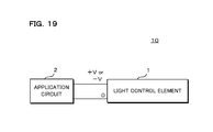
- FIG. 19 is a block diagram illustrating the configuration of an example of non-limiting light control device.
- FIG. 1 is a cross-sectional view illustrating the configuration of a light control element 1 .
- the light control element 1 includes a transparent conductive film 12 , a proton accumulation layer 13 , an inorganic electrolyte layer 14 , an organic electrolyte layer 15 , a catalyst layer 16 , a light control mirror layer 17 , and a protective layer 18 , a transparent conductive film 12 and these layers ( 13 - 18 ) are sequentially laminated on a substrate 11 .
- the light control element 1 includes the transparent conductive film 12 , the proton accumulation layer 13 on the transparent conductive film 12 , the inorganic electrolyte layer 14 on the proton accumulation layer 13 , the organic electrolyte layer 15 on the inorganic electrolyte layer 14 , the catalyst layer 16 on the organic electrolyte layer 15 , the light control mirror layer 17 on the catalyst layer 16 , and the protective layer 18 on the light control mirror layer 17 .
- “on” used in, for example, the expression “on the catalyst layer 16 ” has a meaning of the direction of the layer to be laminated and does not always mean that the layer is arranged adjacent to a layer.
- the expression “the light control mirror layer 17 is formed on the catalyst layer 16 ” indicates a case where the catalyst layer 16 and the light control mirror layer 17 are arranged adjacent to each other and a case where the catalyst layer 16 and the light control mirror layer 17 are arranged so that another layer is disposed between them.
- “on” indicates the upper direction in the drawings.
- FIG. 1 is an explanatory diagram for describing the laminating order of each layer, and the thickness and size of each layer, and thick and thin regions in each layer (magnitude relationship) are not limited to embodiments illustrated in the drawing.
- the substrate 11 is a transparent and plate-shaped member which allows light to be transmitted.
- the substrate 11 is formed, for example, by sheet glass, a resin sheet, or a combination of sheet glass and a resin sheet.
- the transparent conductive film 12 is formed by a conductive material which allows light to be transmitted, for example, indium oxide (In 2 O 3 ), tin oxide (SnO 2 ), an alloy of indium oxide and tin (In 2 O 3 —SnO 2 , abbreviated as ITO), zinc oxide (ZnO), F-doped tin oxide (FTO, fluorine-doped tin oxide), or the like.
- a conductive material which allows light to be transmitted, for example, indium oxide (In 2 O 3 ), tin oxide (SnO 2 ), an alloy of indium oxide and tin (In 2 O 3 —SnO 2 , abbreviated as ITO), zinc oxide (ZnO), F-doped tin oxide (FTO, fluorine-doped tin oxide), or the like.
- the proton accumulation layer 13 is formed by a material which enables accumulation or discharge of protons (hydrogen ions H + ) to be reversibly performed.
- the proton accumulation layer 13 is formed, for example, by a transition metal oxide such as tungsten oxide (WO 3 ), molybdenum oxide (MoO 2 ), niobium oxide (Nb 2 O 5 ), or vanadium oxide (V 2 O 5 ).
- tungsten oxide WO 3
- MoO 2 molybdenum oxide
- Nb 2 O 5 niobium oxide
- V 2 O 5 vanadium oxide
- the proton accumulation layer 13 When the proton accumulation layer 13 is changed from tungsten oxide to tungsten oxide hydride, the proton accumulation layer 13 is changed from the transparent state to the colored state. In addition, in a state where protons are discharged, the proton accumulation layer 13 is changed to tungsten oxide. When the proton accumulation layer 13 is changed from tungsten oxide hydride to tungsten oxide, the proton accumulation layer 13 is changed from the colored state to the transparent state. Protons discharged from the proton accumulation layer 13 move to the light control mirror layer 17 . Furthermore, protons discharged from the light control mirror layer 17 are accumulated in the proton accumulation layer 13 . In this way, the proton accumulation layer 13 is reversibly changed between the colored state and the transparent state depending on accumulation or discharge of protons.
- the inorganic electrolyte layer 14 is formed by an inorganic material which enables protons to pass through, particularly, is desirably formed by a transparent metal oxide.
- the inorganic electrolyte layer 14 is formed by tantalum oxide.
- the organic electrolyte layer 15 is formed by a material which enables protons to pass through, similarly to the inorganic electrolyte layer 14 .
- the organic electrolyte layer 15 is formed by a material which prevents a material (for example, palladium) forming the catalyst layer 16 from being diffused into the inorganic electrolyte layer 14 . Incidentally, the details of the organic electrolyte layer 15 will be described later.
- the catalyst layer 16 is formed by a material that increases a velocity of protons supplied to the light control mirror layer 17 or discharged from the light control mirror layer 17 .
- the catalyst layer 16 is formed by an elemental metal such as palladium, platinum, or silver or an alloy thereof. Further, the catalyst layer 16 may be formed by silicon dioxide in which palladium particles are dispersed.
- the light control mirror layer 17 is formed by a material which changes transmittance of light by occluding protons supplied through the catalyst layer 16 or discharging occluded protons.
- the light control mirror layer 17 is formed, for example, by an alloy of magnesium and calcium (Mg—Ca) or an alloy of magnesium and nickel, titanium, or niobium.
- Mg—Ca magnesium and calcium
- the light control mirror layer 17 is in the transmission state of allowing light to be transmitted.
- protons are discharged
- the light control mirror layer 17 is in a reflection state of allowing light to be reflected.
- protons discharged from the proton accumulation layer 13 move to the light control mirror layer 17 .
- the moved protons are occluded in the light control mirror layer 17 .
- protons discharged from the light control mirror layer 17 move to the proton accumulation layer 13 .
- the moved protons are accumulated in the proton accumulation layer 13 .
- the light control mirror layer 17 is reversibly changed between the transmission state and the reflection state depending on occlusion or discharge of protons.
- the protective layer 18 is formed by a material which prevents the light control mirror layer 17 from being oxidized. Further, the protective layer 18 is formed by a material having a low reflectance of light. If the protective layer 18 is formed by a material having a high reflectance of light, light is reflected by the protective layer 18 even when the light control mirror layer 17 is in the transmission state. The light reflected by the protective layer 18 decreases transmittance of the entire light control element 1 .
- the protective layer 18 is formed, for example, by an aluminum (Al) thin film.
- the protective layer 18 formed by the aluminum thin film can prevent the light control mirror layer 17 from being oxidized. Further, the aluminum thin film is oxidized in air to change to transparent alumina. When the aluminum thin film is changed to transparent alumina, the protective layer 18 does not decrease the transmittance of the entire light control element 1 .
- FIG. 2 is a flowchart illustrating the outline of production processes of the light control element 1 .
- An apparatus for producing the light control element 1 (hereinafter, referred to as the production apparatus) first prepares the substrate 11 of the light control element 1 (step S 1 ).
- the production apparatus forms the transparent conductive film 12 on the substrate 11 (step S 2 ).
- the production apparatus forms the proton accumulation layer 13 on the transparent conductive film 12 (step S 3 ).
- the production apparatus forms the inorganic electrolyte layer 14 on the proton accumulation layer 13 (step S 4 ).
- the production apparatus forms the organic electrolyte layer 15 on the inorganic electrolyte layer 14 (step S 5 ).
- the production apparatus forms the catalyst layer 16 on the organic electrolyte layer 15 (step S 6 ). Then, the production apparatus forms the light control mirror layer 17 on the catalyst layer 16 (step S 7 ). Finally, the production apparatus forms the protective layer 18 on the light control mirror layer 17 (step S 8 ).
- each layer for example, a vacuum evaporation method, a sputtering method, an ion-plating method, and the like are used.
- various printing methods such as a spin coating method, a casting method, a microgravure coating method, a gravure coating method, a bar coating method, a roll coating method, a wire bar coating method, a dip coating method, a slit coating method, a capillary coating method, a spray coating method, a nozzle coating method, a gravure printing method, a screen printing method, a flexographic printing method, an off-set printing method, a reverse printing method, and an inkjet printing method may be used.
- the forming method to be used may be selected depending on materials for forming layers, thicknesses of layers, and the like.
- each layer may not be sequentially laminated but one layer or a plurality of layers may be separately formed and then attached to one another.
- the light control element 1 can be produced by using various known production methods as long as functions of respective layers constituting the light control element 1 are not impaired.
- the organic electrolyte layer 15 of the light control element 1 will be described.
- the catalyst layer 16 is formed by palladium and the inorganic electrolyte layer 14 is formed by tantalum oxide will be described.
- the organic electrolyte layer 15 is provided between the inorganic electrolyte layer 14 and the catalyst layer 16 .
- the organic electrolyte layer 15 is formed by an organic material such as tantalum oxide (Ta 2 O 5 ) formed by a sol-gel method, polyether ether ketone (PEEK), or Nafion®.
- the organic electrolyte layer 15 is formed in order to prevent a material (for example, palladium) forming the catalyst layer 16 from being diffused into the inorganic electrolyte layer 14 .
- tantalum oxide Ta 2 O 5
- tantalum pentoxide in some cases.
- the present inventors conducted intensive studies and found out the reason for production of the defective product.
- the reason is that since electrical resistance of the inorganic electrolyte layer included in the defective product is small, a voltage is not applied effectively so that protons do not move in the light control element.
- the light control element when a voltage is applied between the transparent conductive film and the protective layer, protons move between the proton accumulation layer and the light control mirror layer.
- a proper voltage is not applied between the transparent conductive film and the protective layer, protons do not move.
- a catalyst layer containing palladium is formed on an inorganic electrolyte layer containing tantalum oxide.
- palladium may be diffused into the inorganic electrolyte layer in some cases.
- the diffused palladium decreases the electrical resistance of the inorganic electrolyte layer. Due to the decrease in the electrical resistance, a so-called leak current flows in the inorganic electrolyte layer when a voltage is applied to the inorganic electrolyte layer.
- the total electrical resistance of the conventional light control element may become lower than a determined value in some cases. As a result, even when a voltage is applied to the defective product, protons do not move.
- the electrical resistance of the inorganic electrolyte layer is decreased by diffusion of palladium so that protons do not move, and thus such transition is not performed.
- the light control element 1 of this embodiment has a structure in which the organic electrolyte layer 15 is laminated on the inorganic electrolyte layer 14 and the catalyst layer 16 is further laminated thereon.
- the organic electrolyte layer 15 of the light control element 1 can prevent palladium contained in the catalyst layer 16 from being diffused into the inorganic electrolyte layer 14 when the catalyst layer 16 is laminated in production of a light control element 1 .
- a decrease in electrical resistance in the inorganic electrolyte layer 14 due to the diffusion of palladium does not occur, and thus occurrence of the defective product can be suppressed.
- the occurrence rate of the defective product also referred to as the percent defective of the light control element
- the percent defective of the light control element it is possible to lower the occurrence rate of the defective product (also referred to as the percent defective of the light control element), that is, to suppress a decrease in yield ratio in production of the light control element.
- FIG. 3A is a cross-sectional view illustrating the configuration of a light control element 1 of Example 1.
- FIG. 3A illustrates the configuration of Example 1 (the light control element 1 including the organic electrolyte layer 15 ).
- FIG. 3B is a cross-sectional view illustrating the configuration of a light control element 1 of Comparative Example 1.
- FIG. 3B illustrates the configuration of Comparative Example 1 (the conventional light control element).
- the light control element illustrated in FIG. 3B is, as described above, a defective product in which the light control mirror layer does not normally operate. Incidentally, in FIGS. 3A and 3B , the description of the substrate 11 is omitted.
- the materials of respective layers of the light control element 1 of Example 1 used for verification were as follows.
- the transparent conductive film 12 was formed by ITO and the proton accumulation layer 13 was a tungsten oxide layer formed by a sputtering method.
- the inorganic electrolyte layer 14 was a tantalum oxide layer formed by a sputtering method and the organic electrolyte layer 15 was a tantalum oxide layer formed by a sol-gel method.
- the catalyst layer 16 was formed by palladium.
- the light control mirror layer 17 was formed by an alloy of magnesium and calcium.
- the protective layer 18 was formed by aluminum.
- Comparative Example 1 the materials of Comparative Example 1 were as follows.
- the transparent conductive film 12 was formed by ITO and the proton accumulation layer 13 was a tungsten oxide layer formed by a sputtering method.
- the inorganic electrolyte layer 14 was a tantalum oxide layer formed by a sputtering method.
- the catalyst layer 16 was formed by palladium.
- the light control mirror layer 17 was formed by an alloy of magnesium and calcium.
- the protective layer 18 was formed by aluminum. That is, Comparative Example 1 has the configuration similar to that of Example 1, except that the organic electrolyte layer 15 was not provided.
- V schematically illustrates a circuit applying a voltage
- AC impedance measurement was performed to figure out electrical characteristics of Example 1 and Comparative Example 1.
- the AC impedance measurement is a method of measuring impedance of an analysis target by applying an AC voltage while a frequency is changed, and the identification of the equivalent circuit can be carried out from the measurement result.
- FIG. 4 is a graph showing the result of AC impedance measurement.
- the graph shown in FIG. 4 is a graph called Cole-Cole plot.
- impedances of two light control elements are measured with a plurality of frequencies by using an AC impedance method and the impedance spectra thereof are drawn on a complex plane.
- the vertical axis of FIG. 4 indicates an impedance in the imaginary region and the unit is ⁇ (ohm).
- the horizontal axis of FIG. 4 is an impedance in the real region and the unit is ⁇ (ohm).
- a graph 31 is a graph representing the characteristics of Example 1.
- a graph 32 is a graph representing the characteristics of Comparative Example 1. From the graphs of FIG.
- Comparative Example 1 has the impedance only in the region having a high frequency.
- Example 1 has impedance not only in the region having a high frequency but also in a region C 1 having a low frequency. That is, only response according to charge transfer is observed in Comparative Example 1; on the other hand, response according to mass transfer is also observed in Example 1. In other words, movement of protons does not occur in Comparative Example 1; on the other hand, movement of protons occurs in Example 1.
- the CV measurement is, for example, measurement in which a potential is swept with respect to the observation system by using a triangle wave voltage source and the potential is measured.
- electrochemical reaction such as movement of protons in the light control element can be observed.
- FIG. 5 is an explanatory diagram of CV measurement.
- the relationship between the potential and the current value obtained by CV measurement is represented by the graph.
- the horizontal axis indicates the potential and the unit is V.
- the vertical axis indicates the current and the unit is mA/cm 2 .
- FIG. 5 shows two typical graphs obtained by CV measurement.
- a graph 41 is a graph obtained when electrochemical reaction does not occur.
- a graph 42 is a graph obtained when electrochemical reaction occurs.
- FIG. 6 is a graph showing the result of CV measurement.
- the horizontal axis indicates the potential and the unit is V.
- the vertical axis indicates current and the unit is mA/cm 2 .
- a graph 51 is a graph showing the measurement result of Comparative Example 1.
- a graph 52 is a graph showing the measurement result of Example 1. From the results shown in FIG. 6 , movement of protons is not observed in Comparative Example 1; on the other hand, movement of protons is observed in Example 1.
- the waveform near a peak P 1 represents the observation result corresponding to occlusion of protons of the light control mirror layer 17 .
- the waveform near a peak P 2 represents the observation result corresponding to discharge of protons from the light control mirror layer 17 . Therefore, it is found out that electrochemical reaction occurs in Example 1, but electrochemical reaction does not occur in Comparative Example 1.
- FIG. 7 is a cross-sectional view illustrating the configuration of a light control element 1 of Example 2.
- FIG. 8 is a graph showing the result of CV measurement of Example 2.
- the light control element 1 of Example 2 had the configuration similar to that of Example 1, except that the inorganic electrolyte layer 14 was a tantalum oxide layer formed by an ion-plating method, and the proton accumulation layer 13 was a tungsten oxide layer formed by an ion-plating method.
- the peak corresponding to occlusion of protons of the light control mirror layer 17 and the peak corresponding to discharge of protons from the light control mirror layer 17 were observed.
- the inorganic electrolyte layer 14 is a tantalum oxide layer formed by an ion-plating method and the proton accumulation layer 13 is a tungsten oxide layer formed by an ion-plating method.
- FIG. 9 is a cross-sectional view illustrating the configuration of a light control element 1 of Example 3.
- FIG. 10 is a graph showing the result of CV measurement of Example 3.
- the light control element 1 of Example 3 had the configuration similar to that of Example 1, except that the light control mirror layer 17 was formed by an alloy of magnesium and nickel.
- the peak corresponding to occlusion of protons of the light control mirror layer 17 and the peak corresponding to discharge of protons from the light control mirror layer 17 were observed. Therefore, it is found out that electrochemical reaction occurs by providing the organic electrolyte layer 15 when the light control mirror layer 17 is formed by an alloy of magnesium and nickel.
- FIG. 11 is a cross-sectional view illustrating the configuration of a light control element 1 of Example 4.
- FIG. 12 is a graph showing the result of CV measurement of Example 4.
- Example 4 had the configuration similar to that of Example 1, except that the light control mirror layer 17 was an yttrium layer.
- the peak corresponding to occlusion of protons of the light control mirror layer 17 and the peak corresponding to discharge of protons from the light control mirror layer 17 were observed. Therefore, it is found out that electrochemical reaction occurs by providing the organic electrolyte layer 15 when the light control mirror layer 17 is an yttrium layer.
- FIG. 13 is a cross-sectional view illustrating the configuration of a light control element 1 of Example 5.
- FIG. 14 is a graph showing the result of CV measurement of Example 5.
- Example 5 had the configuration similar to that of Example 1, except that the organic electrolyte layer 15 was a Nafion layer.
- the peak corresponding to occlusion of protons of the light control mirror layer 17 and the peak corresponding to discharge of protons from the light control mirror layer 17 were observed. Therefore, it is found out that electrochemical reaction occurs when the organic electrolyte layer 15 is a Nafion layer.
- FIG. 15 is a cross-sectional view illustrating the configuration of a light control element 1 of Example 6.
- FIG. 16 is a graph showing the result of CV measurement of Example 6.
- Example 6 had the configuration similar to that of Example 1, except that the organic electrolyte layer 15 was formed by a PEEK layer.
- the peak corresponding to occlusion of protons of the light control mirror layer 17 and the peak corresponding to discharge of protons from the light control mirror layer 17 were observed. Therefore, it is found out that electrochemical reaction occurs when the organic electrolyte layer 15 is a PEEK layer.
- FIG. 17 is a cross-sectional view illustrating the configuration of a light control element 1 of Comparative Example 2.
- FIG. 18 is a graph showing the result of CV measurement of Comparative Example 2.
- Comparative Example 2 had the configuration similar to that of Comparative Example 1, except that the proton accumulation layer 13 was a tungsten oxide layer formed by an ion-plating method and the inorganic electrolyte layer 14 was a tantalum oxide layer formed by an ion-plating method.
- the tungsten oxide layer and the tantalum oxide layer formed by an ion-plating method were used and the organic electrolyte layer was not provided, any peaks according to movement of protons were not observed. Therefore, it is found out that electrochemical reaction does not occur when the organic electrolyte layer is not provided.
- the organic electrolyte layer 15 is provided between the inorganic electrolyte layer 14 and the catalyst layer 16 .
- the organic electrolyte layer 15 makes it possible that palladium forming the catalyst layer 16 is prevented from being diffused into the inorganic electrolyte layer 14 when the catalyst layer 16 is laminated in the production processes. Furthermore, it is possible to prevent a problem in that movement of protons does not occur due to the diffusion of palladium when a voltage is applied to the light control element. In this way, when the organic electrolyte layer 15 is provided, a decrease in yield ratio in production of the light control element can be suppressed.
- FIG. 19 is a block diagram illustrating the configuration of a light control device 10 .
- the light control device 10 includes the light control element 1 and an application circuit 2 .
- the application circuit 2 is a circuit applying a voltage between the transparent conductive film 12 and the protective layer 18 of the light control element 1 .
- the application circuit 2 applies a voltage between the transparent conductive film 12 and the light control mirror layer 17 and causes the light control mirror layer 17 to transition from the transmission state to the reflection state or from the reflection state to the transmission state.
- the application circuit 2 If a first output terminal is set to 0 (V), the application circuit 2 enables a second output terminal to be set to +V (V) or ⁇ V (V).
- the application circuit 2 causes the light control mirror layer 17 of the light control element 1 to transition to the reflection state or the transmission state and the proton accumulation layer 13 of the light control element 1 to transition to the colored state or the transparent state.
- the application circuit 2 applies a first voltage (for example, a voltage having a first polarity) to the light control element 1 such that the potential of the protective layer 18 becomes higher than the potential of the transparent conductive film 12 .
- a first voltage for example, a voltage having a first polarity
- the application circuit 2 applies a second voltage different from the first voltage (for example, a voltage having a second polarity different from the first polarity) to the light control element 1 such that the potential of the protective layer 18 becomes lower than the potential of the transparent conductive film 12 .
- a voltage is applied in a direction opposite to the predetermined direction.
- the light control device 10 changes the state of the light control element 1 depending on a voltage output from the application circuit and allows light to be reflected or transmitted.
Abstract
Description
Claims (15)
Applications Claiming Priority (4)
| Application Number | Priority Date | Filing Date | Title |
|---|---|---|---|
| JP2016-005567 | 2016-01-14 | ||
| JP2016005567 | 2016-01-14 | ||
| JP2016168300A JP6894588B2 (en) | 2016-01-14 | 2016-08-30 | Dimming element, dimming equipment, and manufacturing method of dimming element |
| JP2016-168300 | 2016-08-30 |
Publications (2)
| Publication Number | Publication Date |
|---|---|
| US20170205681A1 US20170205681A1 (en) | 2017-07-20 |
| US9995986B2 true US9995986B2 (en) | 2018-06-12 |
Family
ID=59314721
Family Applications (1)
| Application Number | Title | Priority Date | Filing Date |
|---|---|---|---|
| US15/406,048 Active US9995986B2 (en) | 2016-01-14 | 2017-01-13 | Light control element, light control device, and method for producing light control element |
Country Status (2)
| Country | Link |
|---|---|
| US (1) | US9995986B2 (en) |
| CN (1) | CN106970497B (en) |
Citations (3)
| Publication number | Priority date | Publication date | Assignee | Title |
|---|---|---|---|---|
| US7545551B2 (en) * | 2005-09-12 | 2009-06-09 | National Institute Of Advanced Industrial Science And Technology | All-solid-state reflection-controllable electrochromic device and optical switchable component using it |
| US20100188726A1 (en) | 2007-06-18 | 2010-07-29 | National Institute Of Advanced Industrial Science And Tehcnology | All-Solid-State Reflective Dimming Electrochromic Device Having Buffer Layer and Dimmer Member Using the Same |
| US8773746B2 (en) * | 2010-01-08 | 2014-07-08 | National Institute Of Advanced Industrial Science And Technology | All-solid-state reflective dimming electrochromic element sealed with protective layer, and dimming member comprising the same |
Family Cites Families (4)
| Publication number | Priority date | Publication date | Assignee | Title |
|---|---|---|---|---|
| EP1340121A2 (en) * | 2000-11-27 | 2003-09-03 | Koninklijke Philips Electronics N.V. | Electrochromic optical switching device |
| TW201145234A (en) * | 2010-06-14 | 2011-12-16 | J Touch Corp | 2D/3D image switching display device |
| DE112013007836B3 (en) * | 2012-07-20 | 2023-06-22 | Semiconductor Energy Laboratory Co., Ltd. | display device |
| CN104391413B (en) * | 2012-09-03 | 2017-06-27 | 京东方科技集团股份有限公司 | A kind of electrochromic device |
-
2017
- 2017-01-12 CN CN201710023091.4A patent/CN106970497B/en active Active
- 2017-01-13 US US15/406,048 patent/US9995986B2/en active Active
Patent Citations (4)
| Publication number | Priority date | Publication date | Assignee | Title |
|---|---|---|---|---|
| US7545551B2 (en) * | 2005-09-12 | 2009-06-09 | National Institute Of Advanced Industrial Science And Technology | All-solid-state reflection-controllable electrochromic device and optical switchable component using it |
| US20100188726A1 (en) | 2007-06-18 | 2010-07-29 | National Institute Of Advanced Industrial Science And Tehcnology | All-Solid-State Reflective Dimming Electrochromic Device Having Buffer Layer and Dimmer Member Using the Same |
| JP5136978B2 (en) | 2007-06-18 | 2013-02-06 | 独立行政法人産業技術総合研究所 | All-solid-state reflective dimming electrochromic element having buffer layer and dimming member using the same |
| US8773746B2 (en) * | 2010-01-08 | 2014-07-08 | National Institute Of Advanced Industrial Science And Technology | All-solid-state reflective dimming electrochromic element sealed with protective layer, and dimming member comprising the same |
Also Published As
| Publication number | Publication date |
|---|---|
| CN106970497A (en) | 2017-07-21 |
| CN106970497B (en) | 2021-03-09 |
| US20170205681A1 (en) | 2017-07-20 |
Similar Documents
| Publication | Publication Date | Title |
|---|---|---|
| RU2647998C2 (en) | Defect-mitigation layers in electrochromic devices | |
| CN103460303B (en) | Conductive structure, contact panel and manufacture method thereof | |
| US9860981B2 (en) | Transparent conductive film and method for producing same | |
| CN103201105B (en) | Transparent conductive film | |
| CN101765808B (en) | Electrochromic devices and fabrication method | |
| EP2348357A2 (en) | Transparent electrochromic plate and method for manufacture thereof | |
| CN103329035B (en) | Porous electrode sheet and manufacture method thereof and display device | |
| JP2007532940A (en) | Method for powering electrically controlled devices with variable optical and / or energy characteristics | |
| KR20170101702A (en) | Electrochromic device | |
| CN105144045B (en) | Conductive structure and its manufacture method | |
| CN106662950A (en) | Conductive structure and a preparation method therefor | |
| EP2259329A1 (en) | Metal transparent conductors with low sheet resistance | |
| US10198134B2 (en) | Shadow elimination arrangement, touch screen and method for producing the same | |
| KR101849449B1 (en) | Conductive structure body and method for manufacturing the same | |
| CN103578609B (en) | Conductive film | |
| JP2017510847A (en) | Electrowetting device electrodes | |
| EP4073581A1 (en) | Enhanced control of an igu with graded tinting | |
| US20160224151A1 (en) | Electrode to be used in input device and method for producing same | |
| TWI528095B (en) | Electrochromic device and method of manufacturing the same | |
| US9995986B2 (en) | Light control element, light control device, and method for producing light control element | |
| CN102270074B (en) | Electrode structure and manufacture method thereof | |
| CN107660279B (en) | Conductive structure and method for manufacturing same | |
| JP6894588B2 (en) | Dimming element, dimming equipment, and manufacturing method of dimming element | |
| JPH02216131A (en) | Display controller for electrochromic element | |
| JPH0580356A (en) | Production of bidirectional nonlinear resistance element and production of liquid crystal display panel |
Legal Events
| Date | Code | Title | Description |
|---|---|---|---|
| AS | Assignment |
Owner name: NLT TECHNOLOGIES, LTD., JAPAN Free format text: ASSIGNMENT OF ASSIGNORS INTEREST;ASSIGNORS:IMAI, AYUKO;SUMIYOSHI, KEN;REEL/FRAME:040998/0935 Effective date: 20161114 |
|
| STCF | Information on status: patent grant |
Free format text: PATENTED CASE |
|
| AS | Assignment |
Owner name: TIANMA JAPAN, LTD., JAPAN Free format text: CHANGE OF NAME;ASSIGNOR:NLT TECHNOLOGIES, LTD.;REEL/FRAME:050359/0923 Effective date: 20170701 |
|
| AS | Assignment |
Owner name: TIANMA MICROELECTRONICS CO., LTD., CHINA Free format text: ASSIGNMENT OF ASSIGNORS INTEREST;ASSIGNOR:TIANMA JAPAN, LTD.;REEL/FRAME:050395/0931 Effective date: 20190910 |
|
| MAFP | Maintenance fee payment |
Free format text: PAYMENT OF MAINTENANCE FEE, 4TH YEAR, LARGE ENTITY (ORIGINAL EVENT CODE: M1551); ENTITY STATUS OF PATENT OWNER: LARGE ENTITY Year of fee payment: 4 |