US9971369B1 - Voltage regulator - Google Patents
Voltage regulator Download PDFInfo
- Publication number
- US9971369B1 US9971369B1 US15/496,129 US201715496129A US9971369B1 US 9971369 B1 US9971369 B1 US 9971369B1 US 201715496129 A US201715496129 A US 201715496129A US 9971369 B1 US9971369 B1 US 9971369B1
- Authority
- US
- United States
- Prior art keywords
- voltage
- transistor
- terminal
- power
- node
- Prior art date
- Legal status (The legal status is an assumption and is not a legal conclusion. Google has not performed a legal analysis and makes no representation as to the accuracy of the status listed.)
- Active
Links
Images


Classifications
-
- G—PHYSICS
- G05—CONTROLLING; REGULATING
- G05F—SYSTEMS FOR REGULATING ELECTRIC OR MAGNETIC VARIABLES
- G05F1/00—Automatic systems in which deviations of an electric quantity from one or more predetermined values are detected at the output of the system and fed back to a device within the system to restore the detected quantity to its predetermined value or values, i.e. retroactive systems
- G05F1/10—Regulating voltage or current
- G05F1/46—Regulating voltage or current wherein the variable actually regulated by the final control device is dc
- G05F1/56—Regulating voltage or current wherein the variable actually regulated by the final control device is dc using semiconductor devices in series with the load as final control devices
- G05F1/565—Regulating voltage or current wherein the variable actually regulated by the final control device is dc using semiconductor devices in series with the load as final control devices sensing a condition of the system or its load in addition to means responsive to deviations in the output of the system, e.g. current, voltage, power factor
- G05F1/569—Regulating voltage or current wherein the variable actually regulated by the final control device is dc using semiconductor devices in series with the load as final control devices sensing a condition of the system or its load in addition to means responsive to deviations in the output of the system, e.g. current, voltage, power factor for protection
- G05F1/571—Regulating voltage or current wherein the variable actually regulated by the final control device is dc using semiconductor devices in series with the load as final control devices sensing a condition of the system or its load in addition to means responsive to deviations in the output of the system, e.g. current, voltage, power factor for protection with overvoltage detector
-
- G—PHYSICS
- G05—CONTROLLING; REGULATING
- G05F—SYSTEMS FOR REGULATING ELECTRIC OR MAGNETIC VARIABLES
- G05F1/00—Automatic systems in which deviations of an electric quantity from one or more predetermined values are detected at the output of the system and fed back to a device within the system to restore the detected quantity to its predetermined value or values, i.e. retroactive systems
- G05F1/10—Regulating voltage or current
- G05F1/46—Regulating voltage or current wherein the variable actually regulated by the final control device is dc
- G05F1/468—Regulating voltage or current wherein the variable actually regulated by the final control device is dc characterised by reference voltage circuitry, e.g. soft start, remote shutdown
-
- G—PHYSICS
- G05—CONTROLLING; REGULATING
- G05F—SYSTEMS FOR REGULATING ELECTRIC OR MAGNETIC VARIABLES
- G05F1/00—Automatic systems in which deviations of an electric quantity from one or more predetermined values are detected at the output of the system and fed back to a device within the system to restore the detected quantity to its predetermined value or values, i.e. retroactive systems
- G05F1/10—Regulating voltage or current
- G05F1/46—Regulating voltage or current wherein the variable actually regulated by the final control device is dc
- G05F1/56—Regulating voltage or current wherein the variable actually regulated by the final control device is dc using semiconductor devices in series with the load as final control devices
- G05F1/577—Regulating voltage or current wherein the variable actually regulated by the final control device is dc using semiconductor devices in series with the load as final control devices for plural loads
Definitions
- the present invention relates to a voltage regulator, and more particularly to a source and sink voltage regulator for a cascade I/O circuit.
- the circuitry of an integrated circuit (IC) chip usually comprises transistors that withstand low voltages.
- the IC chip comprises 1.8V transistors.
- an output pad of the IC chip provides a higher output voltage (e.g., 3.3V)
- the 1.8V transistors of the I/O circuit are in a cascade connection.
- two P-type transistors in the cascade connection are connected between a power voltage (3.3V) and the output pad. If the I/O circuit provides 0V to the output pad, the source-drain voltages of the P-type transistors are within the withstanding voltage range (i.e., 1.8V).
- N-type transistors in the cascade connection are connected between the output pad and a ground voltage (GND). If the I/O circuit provides 3.3V to the output pad, the source-drain voltages of the N-type transistors are within the withstanding voltage range (i.e., 1.8V.)
- the conventional I/O circuit still has some drawbacks. For example, it is necessary to properly control the gate voltages of the P-type transistors or the N-type transistors. If the gate voltages are not properly controlled, the gate-source voltages of the transistors are possibly beyond the withstanding voltage range and thus the transistors are burnt out.
- An embodiment of the present invention provides a voltage regulator.
- the voltage regulator is connected with an input/output circuit.
- the voltage regulator includes a controlling circuit, a sink voltage generator and a source voltage generator.
- the controlling circuit generates a first reference voltage, a second reference voltage, a first power start control signal and a second power start control signal.
- the sink voltage generator receives the first reference voltage and the first power start control signal.
- the source voltage generator receives the second reference voltage and the second power start control signal.
- FIG. 1 is a schematic circuit diagram illustrating a voltage regulator for a cascade I/O circuit according to an embodiment of the present invention
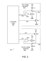
- FIG. 2 is a schematic circuit diagram illustrating the detailed circuitry of the voltage regulator according to the embodiment of the present invention
- FIG. 3A is a schematic circuit diagram illustrating the controlling circuit of the voltage regulator according to the embodiment of the present invention.
- FIG. 3B is a schematic timing waveform diagram illustrating associated signal processed by the voltage regulator according to the embodiment of the present invention.
- FIG. 4A is a schematic circuit diagram illustrating a variant example of the sink voltage generator of the voltage regulator according to the embodiment of the present invention.
- FIG. 4B is a schematic circuit diagram illustrating a variant example of the source voltage generator of the voltage regulator according to the embodiment of the present invention.
- FIG. 4C is a schematic circuit diagram illustrating a variant example of the controlling circuit of the voltage regulator according to the embodiment of the present invention.
- FIG. 1 is a schematic circuit diagram illustrating a voltage regulator for a cascade I/O circuit according to an embodiment of the present invention.
- the cascade input/out (I/O) circuit 100 comprises a pull-up circuit 102 and a pull-down circuit 104 .
- the pull-up circuit 102 comprises two P-type transistors P 1 and P 2 in a cascade connection.
- the two P-type transistors P 1 and P 2 are connected between a power voltage Vcc and an output pad 120 .
- the gate terminals of the P-type transistors P 1 and P 2 receive gate signals Cp 1 and Cp 2 , respectively.
- the pull-down circuit 104 comprises two N-type transistors N 1 and N 2 in a cascade connection.
- the two N-type transistors N 1 and N 2 are connected between the output pad 120 and a ground voltage GND.
- the gate terminals of the N-type transistors N 1 and N 2 receive gate signals Cn 1 and Cn 2 , respectively.
- the pull-up circuit 102 activates the gate signals Cp 1 and Cp 2 to turn on the P-type transistors P 1 and P 2 . Consequently, the power voltage Vcc is transmitted to the output pad 120 . Meanwhile, the pull-down circuit 104 turns off the conduction path between the output pad 120 and the ground voltage GND.
- the pull-down circuit 104 activates the gate signals Cn 1 and Cn 2 to turn on the N-type transistors N 1 and N 2 . Consequently, the ground voltage GND is transmitted to the output pad 120 . Meanwhile, the pull-up circuit 102 turns off the conduction path between the output pad 120 and the power voltage Vcc.
- the voltage regulator 200 provides a sink voltage Vsk (e.g., 1.5V) to the pull-up circuit 102 .
- the sink voltage Vsk is used as the lowest voltage level of the pull-up circuit 102 . Consequently, the operating voltages of all signals of the pull-up circuit 102 are in a range between the power voltage Vcc and the sink voltage Vsk.
- the voltage regulator 200 provides a source voltage Vse (e.g., 1.8V) to the pull-down circuit 104 .
- the source voltage Vse is used as the highest voltage level of the pull-down circuit 104 . Consequently, the operating voltages of all signals of the pull-down circuit 104 are in a range between the source voltage Vse and the ground voltage GND.
- the voltage regulator 200 provides the sink voltage Vsk to the pull-up circuit 102 . Consequently, in the pull-up circuit 102 , the highest voltage level is the power voltage Vcc and the lowest voltage level is the sink voltage Vsk. Similarly, in the normal working state, the voltage regulator 200 provides the source voltage Vse to the pull-down circuit 104 . Consequently, in the pull-down circuit 104 , the highest voltage level is the source voltage Vse and the lowest voltage level is the ground voltage GND.
- the power voltage Vcc is 3.3V
- the sink voltage Vsk is 1.5V
- the source voltage Vse is 1.8V
- the ground voltage GND is 0V.
- the gate signals Cp 1 and Cp 2 of the pull-up circuit 102 are both equal to the sink voltage Vsk (1.5V). Since the P-type transistors P 1 and P 2 are turned on, the power voltage Vcc is transmitted to the output pad 120 . Meanwhile, the gate signal Cn 1 and Cn 2 of the pull-down circuit 104 are equal to the source voltage Vse (1.8V) and the ground voltage GND (0V), respectively. Consequently, the conduction path between the output pad 120 and the ground voltage GND is turned off.
- the gate signal Cn 1 and Cn 2 of the pull-down circuit 104 are both equal to the source voltage Vse (1.8V). Since the N-type transistors N 1 and N 2 are turned on, the ground voltage GND (0V) is transmitted to the output pad 120 . Moreover, in the pull-up circuit 102 , the gate signal Cp 2 and Cp 1 are equal to the sink voltage Vsk (1.5V) and the power voltage Vcc (3.3V), respectively. Consequently, the conduction path between the output pad 120 and the power voltage Vcc is turned off.
- the voltage between any two terminals of the P-type transistor P 1 , the P-type transistor P 2 , the N-type transistor N 1 or the N-type transistor N 2 does not exceed the withstanding voltage range regardless of whether the output pad 120 outputs the high voltage (3.3V) or the low voltage (0V).
- the sink voltage generator 210 comprises an operational amplifier OP 1 , a capacitor C 1 , a transistor Mp 1 and a transistor Mn 1 .
- a positive input terminal of the operational amplifier OP 1 receives a reference voltage Vrp.
- a negative input terminal of the operational amplifier OP 1 is connected with a node a.
- the capacitor C 1 is connected between the power voltage Vcc and the node a.
- the gate terminal of the transistor Mp 1 is connected with an output terminal of the operational amplifier OP 1 .
- a first terminal of the transistor Mp 1 is connected with the node a.
- a second terminal of the transistor Mp 1 is connected with the ground voltage GND.
- the gate terminal of the transistor Mn 1 receives a power start control signal Ctrh.
- a first terminal of the transistor Mn 1 is connected with the node a.
- a second terminal of the transistor Mn 1 is connected with the ground voltage GND.
- the node a generates the sink voltage Vsk.
- the source voltage generator 220 comprises an operational amplifier OP 2 , a capacitor C 2 , a transistor Mp 2 and a transistor Mn 2 .
- a positive input terminal of the operational amplifier OP 2 receives a reference voltage Vrm.
- a negative input terminal of the operational amplifier OP 2 is connected with a node b.
- the capacitor C 2 is connected between the ground voltage GND and the node b.
- the gate terminal of the transistor Mn 2 is connected with an output terminal of the operational amplifier OP 2 .
- a first terminal of the transistor Mn 2 is connected with the node b.
- a second terminal of the transistor Mn 2 is connected with the power voltage Vcc.
- the gate terminal of the transistor Mp 2 receives a power start control signal Ctrl.
- a first terminal of the transistor Mp 2 is connected with the node b.
- a second terminal of the transistor Mp 2 is connected with the ground voltage Vcc.
- the node b generates the source voltage Vse.
- the controlling circuit 230 inactivates the power start control signals Ctrh and Ctrl. Moreover, the controlling circuit 230 provides the reference voltages Vrp and Vrn to the sink voltage generator 210 and the source voltage generator 220 , respectively. According to the reference voltage Vrp, the sink voltage generator 210 generates the sink voltage Vsk. According to the reference voltage Vrn, the source voltage generator 220 generates the source voltage Vse. For example, if the reference voltage Vrp is 1.5V, the sink voltage generator 210 generates the sink voltage Vsk of 1.5V. Similarly, if the reference voltage Vrn is 1.8V, the source voltage generator 220 generates the source voltage Vse of 1.8V.
- the controlling circuit 230 activates the power start control signals Ctrh and Ctrl.
- the ground voltage GND is temporarily used as the sink voltage Vsk by the sink voltage generator 210
- the power voltage Vcc is temporarily used as the source voltage Vse by the source voltage generator 220 .
- FIG. 3A is a schematic circuit diagram illustrating the controlling circuit of the voltage regulator according to the embodiment of the present invention.
- FIG. 3B is a schematic timing waveform diagram illustrating associated signal processed by the voltage regulator according to the embodiment of the present invention.
- the gate terminal of the transistor m 1 is connected with the node d.
- a first terminal of the transistor m 1 is connected with the power voltage Vcc.
- the resistor r 4 is connected with a second terminal of the transistor m 1 and the ground voltage GND.
- a gate terminal of the transistor m 2 is connected with a second terminal of the transistor m 1 .
- a first terminal of the transistor m 2 is connected with the power voltage Vcc.
- the resistor r 5 is connected between a second terminal of the transistor m 2 and the ground voltage GND. Moreover, the second terminal of the transistor m 2 generates the power start control signal Ctrh.
- the voltage regulator 200 After the time point t 1 , the voltage regulator 200 is in a normal working state. Meanwhile, the voltage of the node c is sufficient to turn on the transistor m 3 , and the voltage of the node d is sufficient to turn on the transistor m 1 .
- the source voltage Vse generated by the source voltage generator 220 is maintained at about 1.8V.
- the sink voltage Vsk generated by the sink voltage generator 210 is gradually increased from 0V to 1.5V.
- FIG. 4A is a schematic circuit diagram illustrating a variant example of the sink voltage generator of the voltage regulator according to the embodiment of the present invention.
- the connection between the operational amplifier OP 3 and a transistor Mn 3 of the sink voltage generator 310 is distinguished.
- the other aspects of the sink voltage generator 310 are similar to those of the sink voltage generator 210 of FIG. 2 , and are not redundantly described herein.
- a negative input terminal of the operational amplifier OP 3 receives a reference voltage Vrp.
- a positive terminal of the operational amplifier OP 3 is connected with a node a.
- the gate terminal of the transistor Mn 3 is connected with an output terminal of the operational amplifier OP 3 .
- a first terminal of the transistor Mn 3 is connected with the node a.
- a second terminal of the transistor Mn 3 is connected with the ground voltage GND. Since the operational amplifier OP 3 and the transistor Mn 3 are in a negative feedback connection, the sink voltage Vsk is equal to the reference voltage Vrp.
- FIG. 4B is a schematic circuit diagram illustrating a variant example of the source voltage generator of the voltage regulator according to the embodiment of the present invention.
- the connection between the operational amplifier OP 4 and a transistor Mp 3 of the source voltage generator 320 is distinguished.
- the other aspects of the source voltage generator 320 are similar to those of the source voltage generator 220 of FIG. 2 , and are not redundantly described herein.
- a negative input terminal of the operational amplifier OP 4 receives a reference voltage Vrm.
- a positive terminal of the operational amplifier OP 4 is connected with a node b.
- the gate terminal of the transistor Mp 3 is connected with an output terminal of the operational amplifier OP 4 .
- a first terminal of the transistor Mp 3 is connected with the node b.
- a second terminal of the transistor Mp 3 is connected with the power voltage Vcc. Since the operational amplifier OP 4 and the transistor Mp 3 are in a negative feedback connection, the source voltage Vse is equal to the reference voltage Vrn.
- FIG. 4C is a schematic circuit diagram illustrating a variant example of the controlling circuit of the voltage regulator according to the embodiment of the present invention.
- the controlling circuit 330 further comprises a bandgap circuit 332 , a first comparing circuit CMP 1 and a second comparing circuit CMP 2 .
- the bandgap circuit 332 can accurately output the reference voltages Vrp and Vrn.
- a positive input terminal of the first comparing circuit CMP 1 receives the reference voltage Vrp.
- a negative input terminal of the first comparing circuit CMP 1 receives the power voltage Vcc.
- An output terminal of the first comparing circuit CMP 1 generates the power start control signal Ctrh.
- a negative input terminal of the second comparing circuit CMP 2 receives the reference voltage Vrn.
- a positive terminal of the second comparing circuit CMP 2 receives the power voltage Vcc.
- An output terminal of the second comparing circuit CMP 2 generates the power start control signal Ctrl.
- the controlling circuit 330 activates the power start control signals Ctrh and Ctrl. Since the transistor Mn 1 of the sink voltage generator 210 or 310 is turned on, the ground voltage GND is temporarily used as the sink voltage Vsk by the sink voltage generator 210 or 310 . Moreover, since the transistor Mp 2 of the source voltage generator 220 or 320 is turned on, the power voltage Vcc is temporarily used as the source voltage Vse by the source voltage generator 220 or 320 .
- the controlling circuit 330 inactivates the power start control signals Ctrh and Ctrl. Moreover, the controlling circuit 330 provides the reference voltages Vrp and Vrn to the sink voltage generator 210 or 310 and the source voltage generator 220 or 320 , respectively. According to the reference voltage Vrp, the sink voltage generator 210 or 310 generates the sink voltage Vsk. According to the reference voltage Vrn, the source voltage generator 220 or 320 generates the source voltage Vse.
- the sink voltage generator, the source voltage generator and the controlling circuit of the voltage regulator of different examples may be combined with each other to generate the sink voltage Vsk and the source voltage Vse.
- the controlling circuit 230 of FIG. 3A , the sink voltage generator 310 of FIG. 4A and the voltage regulator 200 of FIG. 2 cooperate with each other to generate the sink voltage Vsk and the source voltage Vse.
- the present invention provides a voltage regulator.
- the voltage regulator provides the sink voltage Vsk and the source voltage Vse to the cascade I/O circuit. Consequently, the voltage between any two terminals of the transistor of the cascade I/O circuit does not exceed the withstanding voltage range. That is, the transistors of the cascade I/O circuit can be normally operated.
- the power voltage Vcc is 3.3V and the withstanding voltage of the transistor is 1.8V. It is noted that the magnitudes of the power voltage and the withstanding voltage may be altered according to the practical requirements. For example, in another embodiment, the power voltage Vcc is 5.0V and the withstanding voltage of the transistor is 3.3V.
Landscapes
- Engineering & Computer Science (AREA)
- Physics & Mathematics (AREA)
- Electromagnetism (AREA)
- General Physics & Mathematics (AREA)
- Radar, Positioning & Navigation (AREA)
- Automation & Control Theory (AREA)
- Continuous-Control Power Sources That Use Transistors (AREA)
Abstract
A voltage regulator is connected with an input/output circuit. The voltage regulator includes a controlling circuit, a sink voltage generator and a source voltage generator. The controlling circuit generates a first reference voltage, a second reference voltage, a first power start control signal and a second power start control signal. The sink voltage generator receives the first reference voltage and the first power start control signal. The source voltage generator receives the second reference voltage and the second power start control signal. When the voltage regulator is in a normal working state, the controlling circuit inactivates the first power start control signal and the second power start control signal, the sink voltage generator generates a sink voltage according to the first reference voltage, and the source voltage generator generates a source voltage according to the second reference voltage.
Description
This application claims the benefit of Taiwanese Patent Application No. 106107087, filed Mar. 3, 2017, the subject matter of which is incorporated herein by reference.
The present invention relates to a voltage regulator, and more particularly to a source and sink voltage regulator for a cascade I/O circuit.
For increasing the operating speed and reducing the power consumption, the circuitry of an integrated circuit (IC) chip usually comprises transistors that withstand low voltages. For example, the IC chip comprises 1.8V transistors.
Since an output pad of the IC chip provides a higher output voltage (e.g., 3.3V), the 1.8V transistors of the I/O circuit are in a cascade connection.
For example, in the I/O circuit, two P-type transistors in the cascade connection are connected between a power voltage (3.3V) and the output pad. If the I/O circuit provides 0V to the output pad, the source-drain voltages of the P-type transistors are within the withstanding voltage range (i.e., 1.8V).
Similarly, in the I/O circuit, two N-type transistors in the cascade connection are connected between the output pad and a ground voltage (GND). If the I/O circuit provides 3.3V to the output pad, the source-drain voltages of the N-type transistors are within the withstanding voltage range (i.e., 1.8V.)
However, the conventional I/O circuit still has some drawbacks. For example, it is necessary to properly control the gate voltages of the P-type transistors or the N-type transistors. If the gate voltages are not properly controlled, the gate-source voltages of the transistors are possibly beyond the withstanding voltage range and thus the transistors are burnt out.
An embodiment of the present invention provides a voltage regulator. The voltage regulator is connected with an input/output circuit. The voltage regulator includes a controlling circuit, a sink voltage generator and a source voltage generator. The controlling circuit generates a first reference voltage, a second reference voltage, a first power start control signal and a second power start control signal. The sink voltage generator receives the first reference voltage and the first power start control signal. The source voltage generator receives the second reference voltage and the second power start control signal. When the voltage regulator is in a normal working state, the controlling circuit inactivates the first power start control signal and the second power start control signal, the sink voltage generator generates a sink voltage according to the first reference voltage, and the source voltage generator generates a source voltage according to the second reference voltage.
Numerous objects, features and advantages of the present invention will be readily apparent upon a reading of the following detailed description of embodiments of the present invention when taken in conjunction with the accompanying drawings. However, the drawings employed herein are for the purpose of descriptions and should not be regarded as limiting.
The above objects and advantages of the present invention will become more readily apparent to those ordinarily skilled in the art after reviewing the following detailed description and accompanying drawings, in which:
The pull-up circuit 102 comprises two P-type transistors P1 and P2 in a cascade connection. The two P-type transistors P1 and P2 are connected between a power voltage Vcc and an output pad 120. Moreover, the gate terminals of the P-type transistors P1 and P2 receive gate signals Cp1 and Cp2, respectively.
The pull-down circuit 104 comprises two N-type transistors N1 and N2 in a cascade connection. The two N-type transistors N1 and N2 are connected between the output pad 120 and a ground voltage GND.
Moreover, the gate terminals of the N-type transistors N1 and N2 receive gate signals Cn1 and Cn2, respectively.
When the cascade I/O circuit 100 intends to output a power voltage Vcc to the output pad 120, the pull-up circuit 102 activates the gate signals Cp1 and Cp2 to turn on the P-type transistors P1 and P2. Consequently, the power voltage Vcc is transmitted to the output pad 120. Meanwhile, the pull-down circuit 104 turns off the conduction path between the output pad 120 and the ground voltage GND.
When the cascade I/O circuit 100 intends to output the ground voltage GND to the output pad 120, the pull-down circuit 104 activates the gate signals Cn1 and Cn2 to turn on the N-type transistors N1 and N2. Consequently, the ground voltage GND is transmitted to the output pad 120. Meanwhile, the pull-up circuit 102 turns off the conduction path between the output pad 120 and the power voltage Vcc.
If the gate signal Cp1 or Cp2 generated by the pull-up circuit 102 is improper, the source-drain voltage of the P-type transistor P1 or P2 is possibly beyond the withstanding voltage range. For avoiding this problem, the voltage regulator 200 provides a sink voltage Vsk (e.g., 1.5V) to the pull-up circuit 102. The sink voltage Vsk is used as the lowest voltage level of the pull-up circuit 102. Consequently, the operating voltages of all signals of the pull-up circuit 102 are in a range between the power voltage Vcc and the sink voltage Vsk.
Similarly, if the gate signal Cn1 or Cn2 generated by the pull-down circuit 104 is improper, the source-drain voltage of the N-type transistors N1 or N2 is possibly beyond the withstanding voltage range. For avoiding this problem, the voltage regulator 200 provides a source voltage Vse (e.g., 1.8V) to the pull-down circuit 104. The source voltage Vse is used as the highest voltage level of the pull-down circuit 104. Consequently, the operating voltages of all signals of the pull-down circuit 104 are in a range between the source voltage Vse and the ground voltage GND.
That is, in the normal working state, the voltage regulator 200 provides the sink voltage Vsk to the pull-up circuit 102. Consequently, in the pull-up circuit 102, the highest voltage level is the power voltage Vcc and the lowest voltage level is the sink voltage Vsk. Similarly, in the normal working state, the voltage regulator 200 provides the source voltage Vse to the pull-down circuit 104. Consequently, in the pull-down circuit 104, the highest voltage level is the source voltage Vse and the lowest voltage level is the ground voltage GND.
The operations of the cascade I/O circuit 100 will be described as follows. For example, the power voltage Vcc is 3.3V, the sink voltage Vsk is 1.5V, the source voltage Vse is 1.8V, and the ground voltage GND is 0V.
When the cascade I/O circuit 100 outputs the power voltage Vcc (3.3V) to the output pad 120, the gate signals Cp1 and Cp2 of the pull-up circuit 102 are both equal to the sink voltage Vsk (1.5V). Since the P-type transistors P1 and P2 are turned on, the power voltage Vcc is transmitted to the output pad 120. Meanwhile, the gate signal Cn1 and Cn2 of the pull-down circuit 104 are equal to the source voltage Vse (1.8V) and the ground voltage GND (0V), respectively. Consequently, the conduction path between the output pad 120 and the ground voltage GND is turned off.
When the cascade I/O circuit 100 outputs the ground voltage GND (0V) to the output pad 120, the gate signal Cn1 and Cn2 of the pull-down circuit 104 are both equal to the source voltage Vse (1.8V). Since the N-type transistors N1 and N2 are turned on, the ground voltage GND (0V) is transmitted to the output pad 120. Moreover, in the pull-up circuit 102, the gate signal Cp2 and Cp1 are equal to the sink voltage Vsk (1.5V) and the power voltage Vcc (3.3V), respectively. Consequently, the conduction path between the output pad 120 and the power voltage Vcc is turned off.
From the above descriptions, the voltage between any two terminals of the P-type transistor P1, the P-type transistor P2, the N-type transistor N1 or the N-type transistor N2 does not exceed the withstanding voltage range regardless of whether the output pad 120 outputs the high voltage (3.3V) or the low voltage (0V).
The sink voltage generator 210 comprises an operational amplifier OP1, a capacitor C1, a transistor Mp1 and a transistor Mn1. A positive input terminal of the operational amplifier OP1 receives a reference voltage Vrp. A negative input terminal of the operational amplifier OP1 is connected with a node a. The capacitor C1 is connected between the power voltage Vcc and the node a. The gate terminal of the transistor Mp1 is connected with an output terminal of the operational amplifier OP1. A first terminal of the transistor Mp1 is connected with the node a. A second terminal of the transistor Mp1 is connected with the ground voltage GND. The gate terminal of the transistor Mn1 receives a power start control signal Ctrh. A first terminal of the transistor Mn1 is connected with the node a. A second terminal of the transistor Mn1 is connected with the ground voltage GND. Moreover, the node a generates the sink voltage Vsk.
The source voltage generator 220 comprises an operational amplifier OP2, a capacitor C2, a transistor Mp2 and a transistor Mn2. A positive input terminal of the operational amplifier OP2 receives a reference voltage Vrm. A negative input terminal of the operational amplifier OP2 is connected with a node b. The capacitor C2 is connected between the ground voltage GND and the node b. The gate terminal of the transistor Mn2 is connected with an output terminal of the operational amplifier OP2. A first terminal of the transistor Mn2 is connected with the node b. A second terminal of the transistor Mn2 is connected with the power voltage Vcc. The gate terminal of the transistor Mp2 receives a power start control signal Ctrl. A first terminal of the transistor Mp2 is connected with the node b. A second terminal of the transistor Mp2 is connected with the ground voltage Vcc. Moreover, the node b generates the source voltage Vse.
In the normal working state of the voltage regulator 200, the controlling circuit 230 inactivates the power start control signals Ctrh and Ctrl. Moreover, the controlling circuit 230 provides the reference voltages Vrp and Vrn to the sink voltage generator 210 and the source voltage generator 220, respectively. According to the reference voltage Vrp, the sink voltage generator 210 generates the sink voltage Vsk. According to the reference voltage Vrn, the source voltage generator 220 generates the source voltage Vse. For example, if the reference voltage Vrp is 1.5V, the sink voltage generator 210 generates the sink voltage Vsk of 1.5V. Similarly, if the reference voltage Vrn is 1.8V, the source voltage generator 220 generates the source voltage Vse of 1.8V.
After the voltage regulator 200 is powered on and during a transient period of the voltage regulator 200, the controlling circuit 230 activates the power start control signals Ctrh and Ctrl. Under this circumstance, the ground voltage GND is temporarily used as the sink voltage Vsk by the sink voltage generator 210, and the power voltage Vcc is temporarily used as the source voltage Vse by the source voltage generator 220.
After the voltage regulator 200 is powered on and during the transient period of the voltage regulator 200, the transistor Mn1 of the sink voltage generator 210 is turned on and thus the ground voltage GND is used as the sink voltage Vsk. In addition, the transistor Mp2 of the source voltage generator 220 is turned on, and thus the power voltage Vcc is used as the source voltage Vse.
In the normal working state of the voltage regulator 200, the transistor Mn1 of the sink voltage generator 210 is turned off. Since the operational amplifier OP1 and the transistor Mp1 are in a negative feedback connection, the sink voltage Vsk is equal to the reference voltage Vrp. In addition, the transistor Mp2 of the source voltage generator 220 is turned off. Since the operational amplifier OP2 and the transistor Mn2 are in a negative feedback connection, the source voltage Vse is equal to the reference voltage Vrn. For example, if the reference voltage Vrp is 1.5V, the sink voltage generator 210 generates the sink voltage Vsk of 1.5V. Similarly, if the reference voltage Vrn is 1.8V, the source voltage generator 220 generates the source voltage Vse of 1.8V.
The controlling circuit 230 comprises resistors r1˜r7 and transistors m1˜m4. The resistor r1 is connected between the power voltage Vcc and a node c. The resistor r2 is connected between the node c and a node d. The resistor r3 is arranged between the node d and the ground voltage GND. That is, the resistors r1, r2 and r3 are connected between the power voltage Vcc and the ground voltage GND, and collaboratively formed as a voltage divider. Consequently, the node c generates the reference voltage Vrn, and the node d generates the reference voltage Vrp.
The gate terminal of the transistor m1 is connected with the node d. A first terminal of the transistor m1 is connected with the power voltage Vcc. The resistor r4 is connected with a second terminal of the transistor m1 and the ground voltage GND. A gate terminal of the transistor m2 is connected with a second terminal of the transistor m1. A first terminal of the transistor m2 is connected with the power voltage Vcc. The resistor r5 is connected between a second terminal of the transistor m2 and the ground voltage GND. Moreover, the second terminal of the transistor m2 generates the power start control signal Ctrh.
The gate terminal of the transistor m3 is connected with the node c. A first terminal of the transistor m3 is connected with the ground voltage GND. The resistor r6 is connected with a second terminal of the transistor m3 and the power voltage Vcc. A gate terminal of the transistor m4 is connected with the second terminal of the transistor m3. A first terminal of the transistor m4 is connected with the ground voltage GND. The resistor r7 is connected between a second terminal of the transistor m4 and the power voltage Vcc. Moreover, the second terminal of the transistor m4 generates the power start control signal Ctrl.
Please refer to FIG. 3B . At the time point to, the voltage regulator 200 is powered on. Consequently, the power voltage Vcc is gradually increased from 0V to 3.3V.
The time interval between the time point t0 and the time point t1 is a transient period. The duration of the time interval is about 10 ms˜20 ms. In the transient period, the power voltage Vcc is gradually increased, and the reference voltage Vrn at the node c and the reference voltage Vrp at the node d are gradually increased. Meanwhile, the voltage of the node c is insufficient to turn on the transistor m3, and the voltage of the node d is insufficient to turn on the transistor m1.
Since the transistor m3 is turned off, the transistor m4 is turned on. Meanwhile, the power start control signal Ctrl is substantially equal to the ground voltage GND (0V). That is, the P-type transistor Mp2 of the source voltage generator 220 is turned on in response to a low voltage level. Since the transistor m1 is turned off, the transistor m2 is turned on. Meanwhile, the power start control signal Ctrh is substantially equal to the power voltage Vcc. That is, the N-type transistor Mn1 of the sink voltage generator 210 is turned on in response to a high voltage level.
After the time point t1, the voltage regulator 200 is in a normal working state. Meanwhile, the voltage of the node c is sufficient to turn on the transistor m3, and the voltage of the node d is sufficient to turn on the transistor m1.
Since the transistor m3 is turned on, the transistor m4 is turned off. Meanwhile, the power start control signal Ctrl is substantially equal to the power voltage Vcc. That is, the P-type transistor Mp2 of the source voltage generator 220 is turned off in response to the high voltage level. Since the transistor m1 is turned on, the transistor m2 is turned off. Meanwhile, the power start control signal Ctrh is equal to the ground voltage GND (0V). That is, the N-type transistor Mn1 of the sink voltage generator 210 is turned off in response to the low voltage level.
According to the reference voltage Vrn, the source voltage Vse generated by the source voltage generator 220 is maintained at about 1.8V. According to the reference voltage Vrp, the sink voltage Vsk generated by the sink voltage generator 210 is gradually increased from 0V to 1.5V.
It is noted that the sink voltage generator 210, the source voltage generator 220 and the controlling circuit 230 of the voltage regulator 200 may be modified while retaining the teaching of the present invention.
A negative input terminal of the operational amplifier OP3 receives a reference voltage Vrp. A positive terminal of the operational amplifier OP3 is connected with a node a. The gate terminal of the transistor Mn3 is connected with an output terminal of the operational amplifier OP3. A first terminal of the transistor Mn3 is connected with the node a. A second terminal of the transistor Mn3 is connected with the ground voltage GND. Since the operational amplifier OP3 and the transistor Mn3 are in a negative feedback connection, the sink voltage Vsk is equal to the reference voltage Vrp.
A negative input terminal of the operational amplifier OP4 receives a reference voltage Vrm. A positive terminal of the operational amplifier OP4 is connected with a node b. The gate terminal of the transistor Mp3 is connected with an output terminal of the operational amplifier OP4. A first terminal of the transistor Mp3 is connected with the node b. A second terminal of the transistor Mp3 is connected with the power voltage Vcc. Since the operational amplifier OP4 and the transistor Mp3 are in a negative feedback connection, the source voltage Vse is equal to the reference voltage Vrn.
The bandgap circuit 332 can accurately output the reference voltages Vrp and Vrn. A positive input terminal of the first comparing circuit CMP1 receives the reference voltage Vrp. A negative input terminal of the first comparing circuit CMP1 receives the power voltage Vcc. An output terminal of the first comparing circuit CMP1 generates the power start control signal Ctrh. A negative input terminal of the second comparing circuit CMP2 receives the reference voltage Vrn. A positive terminal of the second comparing circuit CMP2 receives the power voltage Vcc. An output terminal of the second comparing circuit CMP2 generates the power start control signal Ctrl.
Similarly, after the voltage regulator 200 is powered on and during a transient period of the voltage regulator 200, the controlling circuit 330 activates the power start control signals Ctrh and Ctrl. Since the transistor Mn1 of the sink voltage generator 210 or 310 is turned on, the ground voltage GND is temporarily used as the sink voltage Vsk by the sink voltage generator 210 or 310. Moreover, since the transistor Mp2 of the source voltage generator 220 or 320 is turned on, the power voltage Vcc is temporarily used as the source voltage Vse by the source voltage generator 220 or 320.
During the normal operations of the voltage regulator 200, the controlling circuit 330 inactivates the power start control signals Ctrh and Ctrl. Moreover, the controlling circuit 330 provides the reference voltages Vrp and Vrn to the sink voltage generator 210 or 310 and the source voltage generator 220 or 320, respectively. According to the reference voltage Vrp, the sink voltage generator 210 or 310 generates the sink voltage Vsk. According to the reference voltage Vrn, the source voltage generator 220 or 320 generates the source voltage Vse.
Generally, the sink voltage generator, the source voltage generator and the controlling circuit of the voltage regulator of different examples may be combined with each other to generate the sink voltage Vsk and the source voltage Vse. For example, in an embodiment, the controlling circuit 230 of FIG. 3A , the sink voltage generator 310 of FIG. 4A and the voltage regulator 200 of FIG. 2 cooperate with each other to generate the sink voltage Vsk and the source voltage Vse.
From the above descriptions, the present invention provides a voltage regulator. The voltage regulator provides the sink voltage Vsk and the source voltage Vse to the cascade I/O circuit. Consequently, the voltage between any two terminals of the transistor of the cascade I/O circuit does not exceed the withstanding voltage range. That is, the transistors of the cascade I/O circuit can be normally operated.
In the above embodiments, the power voltage Vcc is 3.3V and the withstanding voltage of the transistor is 1.8V. It is noted that the magnitudes of the power voltage and the withstanding voltage may be altered according to the practical requirements. For example, in another embodiment, the power voltage Vcc is 5.0V and the withstanding voltage of the transistor is 3.3V.
While the invention has been described in terms of what is presently considered to be the most practical and preferred embodiments, it is to be understood that the invention needs not be limited to the disclosed embodiment. On the contrary, it is intended to cover various modifications and similar arrangements included within the spirit and scope of the appended claims which are to be accorded with the broadest interpretation so as to encompass all such modifications and similar structures.
Claims (9)
1. A voltage regulator connected with an input/output circuit, the voltage regulator comprising:
a controlling circuit generating a first reference voltage, a second reference voltage, a first power start control signal and a second power start control signal;
a sink voltage generator receiving the first reference voltage and the first power start control signal; and
a source voltage generator receiving the second reference voltage and the second power start control signal,
wherein when the voltage regulator is in a normal working state, the controlling circuit inactivates the first power start control signal and the second power start control signal, the sink voltage generator generates a sink voltage according to the first reference voltage, and the source voltage generator generates a source voltage according to the second reference voltage.
2. The voltage regulator as claimed in claim 1 , wherein the input/output circuit comprises:
a pull-up circuit receiving a power voltage and the sink voltage, so that an operating voltage of the pull-up circuit is in a range between the power voltage and the sink voltage; and
a pull-down circuit receiving the source voltage and a ground voltage, so that an operating voltage of the pull-down circuit is in a range between the source voltage and the ground voltage.
3. The voltage regulator as claimed in claim 2 , wherein the pull-up circuit comprises a first P-type transistor and a second P-type transistor in a cascade connection, wherein the first P-type transistor and the second P-type transistor are connected between the power voltage and an output pad, a gate terminal of the first P-type transistor receives a first gate signal, and a gate terminal of the second P-type transistor receives a second gate signal.
4. The voltage regulator as claimed in claim 3 , wherein the pull-down circuit comprises a first N-type transistor and a second N-type transistor in a cascade connection, wherein the first N-type transistor and the second N-type transistor are connected between the ground voltage and the output pad, a gate terminal of the first N-type transistor receives a third gate signal, and a gate terminal of the second N-type transistor receives a fourth gate signal.
5. The voltage regulator as claimed in claim 1 , wherein before the normal working state and during a transient period, the controlling circuit activates the first power start control signal and the second power start control signal, so that a ground voltage is used as the sink voltage by the sink voltage generator and a power voltage is used as the source voltage by the source voltage generator.
6. The voltage regulator as claimed in claim 5 , wherein the sink voltage generator comprises:
an operational amplifier, wherein a first input terminal of the operational amplifier receives the first reference voltage, and a second input terminal of the operational amplifier is connected with a node a;
a first transistor, wherein a gate terminal of the first transistor is connected with an output terminal of the operational amplifier, a first terminal of the first transistor is connected with the node a, and a second terminal of the first transistor receives the ground voltage;
a capacitor connected between the power voltage and the node a; and
a second transistor, wherein a gate terminal of the second transistor receives the first power start control signal, a first terminal of the second transistor is connected with the node a, and a second terminal of the second transistor receives the ground voltage.
7. The voltage regulator as claimed in claim 5 , wherein the sink voltage generator comprises:
an operational amplifier, wherein a first input terminal of the operational amplifier receives the second reference voltage, and a second input terminal of the operational amplifier is connected with a node b;
a first transistor, wherein a gate terminal of the first transistor is connected with an output terminal of the operational amplifier, a first terminal of the first transistor is connected with the node b, and a second terminal of the first transistor receives the power voltage;
a capacitor connected between the ground voltage and the node b; and
a second transistor, wherein a gate terminal of the second transistor receives the second power start control signal, a first terminal of the second transistor is connected with the node b, and a second terminal of the second transistor receives the power voltage.
8. The voltage regulator as claimed in claim 5 , wherein the controlling circuit comprises:
a bandgap circuit generating the first reference voltage and the second reference voltage;
a first comparing circuit, wherein a first input terminal of the first comparing circuit receives the power voltage, a second input terminal of the first comparing circuit receives the first reference voltage, and an output terminal of the first comparing circuit generates the first power start control signal; and
a second comparing circuit, wherein a first input terminal of the second comparing circuit receives the power voltage, a second input terminal of the second comparing circuit receives the second reference voltage, and an output terminal of the second comparing circuit generates the second power start control signal.
9. The voltage regulator as claimed in claim 5 , wherein the controlling circuit comprises:
a first resistor connected between the power voltage and a node c;
a second resistor connected between the node c and a node d;
a third resistor connected between the node d and the ground voltage, wherein the node d generates the first reference voltage, and the node c generates the second reference voltage;
a first transistor, wherein a gate terminal of the first transistor is connected with the node d, and a first terminal of the first transistor receives the power voltage;
a fourth resistor connected between a second terminal of the first transistor and the ground voltage;
a second transistor, wherein a gate terminal of the second transistor is connected with a second terminal of the first transistor, and a first terminal of the second transistor receives the power voltage;
a fifth resistor connected between a second terminal of the second transistor and the ground voltage, wherein the second terminal of the second transistor generates the first power start control signal;
a third transistor, wherein a gate terminal of the third transistor is connected with the node c, and a first terminal of the third transistor receives the ground voltage;
a sixth resistor connected between a second terminal of the third transistor and the power voltage;
a fourth transistor, wherein a gate terminal of the fourth transistor is connected with the second terminal of the third transistor, and a first terminal of the fourth transistor receives the ground voltage; and
a seventh resistor connected between a second terminal of the fourth transistor and the power voltage, wherein the second terminal of the fourth transistor generates the second power start control signal.
Applications Claiming Priority (2)
| Application Number | Priority Date | Filing Date | Title |
|---|---|---|---|
| TW106107087A | 2017-03-03 | ||
| TW106107087A TWI630469B (en) | 2017-03-03 | 2017-03-03 | Voltage regulator |
Publications (1)
| Publication Number | Publication Date |
|---|---|
| US9971369B1 true US9971369B1 (en) | 2018-05-15 |
Family
ID=62091474
Family Applications (1)
| Application Number | Title | Priority Date | Filing Date |
|---|---|---|---|
| US15/496,129 Active US9971369B1 (en) | 2017-03-03 | 2017-04-25 | Voltage regulator |
Country Status (3)
| Country | Link |
|---|---|
| US (1) | US9971369B1 (en) |
| CN (1) | CN108536211B (en) |
| TW (1) | TWI630469B (en) |
Families Citing this family (9)
| Publication number | Priority date | Publication date | Assignee | Title |
|---|---|---|---|---|
| WO2018102190A1 (en) | 2016-11-29 | 2018-06-07 | Blackmore Sensors and Analytics Inc. | Method and system for classification of an object in a point cloud data set |
| KR102399757B1 (en) | 2016-11-30 | 2022-05-18 | 블랙모어 센서스 앤드 애널리틱스, 엘엘씨 | Method and system for doppler detection and doppler correction of optical chirped range detection |
| WO2018125438A2 (en) | 2016-11-30 | 2018-07-05 | Blackmore Sensors and Analytics Inc. | Method and system for adaptive scanning with optical ranging systems |
| KR102380943B1 (en) | 2016-11-30 | 2022-03-30 | 블랙모어 센서스 앤드 애널리틱스, 엘엘씨 | Method and system for automatic real-time adaptive scanning with optical ranging systems |
| US10422880B2 (en) | 2017-02-03 | 2019-09-24 | Blackmore Sensors and Analytics Inc. | Method and system for doppler detection and doppler correction of optical phase-encoded range detection |
| US10401495B2 (en) | 2017-07-10 | 2019-09-03 | Blackmore Sensors and Analytics Inc. | Method and system for time separated quadrature detection of doppler effects in optical range measurements |
| JP2021515241A (en) | 2018-04-23 | 2021-06-17 | ブラックモア センサーズ アンド アナリティクス エルエルシー | Control methods and systems for autonomous vehicles using coherent distance Doppler optical sensors |
| US11822010B2 (en) | 2019-01-04 | 2023-11-21 | Blackmore Sensors & Analytics, Llc | LIDAR system |
| US11137785B2 (en) | 2020-02-11 | 2021-10-05 | Taiwan Semiconductor Manufacturing Company Limited | On-chip power regulation system for MRAM operation |
Citations (8)
| Publication number | Priority date | Publication date | Assignee | Title |
|---|---|---|---|---|
| US5608312A (en) | 1995-04-17 | 1997-03-04 | Linfinity Microelectronics, Inc. | Source and sink voltage regulator for terminators |
| US6429716B1 (en) * | 1998-12-14 | 2002-08-06 | Ati International Srl | Pre-buffer voltage level shifting circuit and method |
| US6479972B1 (en) | 2000-09-11 | 2002-11-12 | Elite Semiconductor Memory Technology Inc. | Voltage regulator for supplying power to internal circuits |
| US7002379B2 (en) | 2001-01-09 | 2006-02-21 | Broadcom Corporation | I/O circuit using low voltage transistors which can tolerate high voltages even when power supplies are powered off |
| US7570088B1 (en) * | 2005-12-01 | 2009-08-04 | Nvidia Corporation | Input/output buffer for wide supply voltage range |
| US7714553B2 (en) | 2008-02-21 | 2010-05-11 | Mediatek Inc. | Voltage regulator having fast response to abrupt load transients |
| US7843222B1 (en) * | 2009-08-06 | 2010-11-30 | Etron Technology, Inc. | Buffer-driving circuit capable of increasing responding speed and prolonging lifespan, buffer, and method thereof |
| TW201306479A (en) | 2011-07-26 | 2013-02-01 | Global Unichip Corp | Power control circuit and associated power-off control method |
Family Cites Families (6)
| Publication number | Priority date | Publication date | Assignee | Title |
|---|---|---|---|---|
| US6160430A (en) * | 1999-03-22 | 2000-12-12 | Ati International Srl | Powerup sequence artificial voltage supply circuit |
| TWI263875B (en) * | 2004-09-13 | 2006-10-11 | Faraday Tech Corp | Voltage regulator |
| US7619444B1 (en) * | 2005-12-08 | 2009-11-17 | Nvidia Corporation | Circuit technique to prevent device overstress |
| US7646108B2 (en) * | 2006-09-29 | 2010-01-12 | Intel Corporation | Multiple output voltage regulator |
| US20090039711A1 (en) * | 2007-08-08 | 2009-02-12 | Advanced Analogic Technologies, Inc. | Dual-Polarity Multi-Output DC/DC Converters and Voltage Regulators |
| CN104020811B (en) * | 2014-06-11 | 2016-03-02 | 深圳市威益德科技有限公司 | Plurality of voltages regulator circuit |
-
2017
- 2017-03-03 TW TW106107087A patent/TWI630469B/en active
- 2017-04-14 CN CN201710243089.8A patent/CN108536211B/en active Active
- 2017-04-25 US US15/496,129 patent/US9971369B1/en active Active
Patent Citations (8)
| Publication number | Priority date | Publication date | Assignee | Title |
|---|---|---|---|---|
| US5608312A (en) | 1995-04-17 | 1997-03-04 | Linfinity Microelectronics, Inc. | Source and sink voltage regulator for terminators |
| US6429716B1 (en) * | 1998-12-14 | 2002-08-06 | Ati International Srl | Pre-buffer voltage level shifting circuit and method |
| US6479972B1 (en) | 2000-09-11 | 2002-11-12 | Elite Semiconductor Memory Technology Inc. | Voltage regulator for supplying power to internal circuits |
| US7002379B2 (en) | 2001-01-09 | 2006-02-21 | Broadcom Corporation | I/O circuit using low voltage transistors which can tolerate high voltages even when power supplies are powered off |
| US7570088B1 (en) * | 2005-12-01 | 2009-08-04 | Nvidia Corporation | Input/output buffer for wide supply voltage range |
| US7714553B2 (en) | 2008-02-21 | 2010-05-11 | Mediatek Inc. | Voltage regulator having fast response to abrupt load transients |
| US7843222B1 (en) * | 2009-08-06 | 2010-11-30 | Etron Technology, Inc. | Buffer-driving circuit capable of increasing responding speed and prolonging lifespan, buffer, and method thereof |
| TW201306479A (en) | 2011-07-26 | 2013-02-01 | Global Unichip Corp | Power control circuit and associated power-off control method |
Non-Patent Citations (1)
| Title |
|---|
| Taiwan Intellectual Property Office, "Office Action", dated Nov. 24, 2017. |
Also Published As
| Publication number | Publication date |
|---|---|
| CN108536211B (en) | 2019-12-24 |
| TW201833706A (en) | 2018-09-16 |
| TWI630469B (en) | 2018-07-21 |
| CN108536211A (en) | 2018-09-14 |
Similar Documents
| Publication | Publication Date | Title |
|---|---|---|
| US9971369B1 (en) | Voltage regulator | |
| US9786340B2 (en) | Driving circuit for non-volatile memory | |
| US9442502B2 (en) | Voltage regulator with soft-start circuit | |
| US9633734B1 (en) | Driving circuit for non-volatile memory | |
| US10454466B1 (en) | Biasing cascode transistors of an output buffer circuit for operation over a wide range of supply voltages | |
| US7579882B2 (en) | Output buffer circuit eliminating high voltage insulated transistor and level shift circuit, and an electronic device using the output buffer circuit | |
| JP5690341B2 (en) | Integrated circuit adapted to be selectively AC or DC coupled | |
| JP2008532108A (en) | Voltage regulator with bypass mode | |
| JP5743850B2 (en) | Integrated circuit | |
| US20150188436A1 (en) | Semiconductor Device | |
| US8653878B2 (en) | Voltage switch circuit produced by logic circuit manufacturing process capable of withstanding high voltage stress | |
| US9018986B2 (en) | Output buffers | |
| US8957708B2 (en) | Output buffer and semiconductor device | |
| US6936998B2 (en) | Power glitch free internal voltage generation circuit | |
| US7126391B1 (en) | Power on reset circuits | |
| US7710151B2 (en) | Level shifter circuit | |
| JP2011188361A (en) | Power-on reset circuit | |
| US9753515B2 (en) | Anti-deadlock circuit for voltage regulator and associated power system | |
| US10911044B1 (en) | Wide range output driver circuit for semiconductor device | |
| US10719097B1 (en) | Voltage regulation circuit suitable to provide output voltage to core circuit | |
| KR102521572B1 (en) | Electrostatic discharge circuit and electrostatic discharge control system | |
| US20150162912A1 (en) | Level shifter | |
| US11271551B2 (en) | Level shifter | |
| US7482846B2 (en) | Pull-up devices | |
| JP4726881B2 (en) | Output buffer circuit and interface circuit using output buffer circuit |
Legal Events
| Date | Code | Title | Description |
|---|---|---|---|
| AS | Assignment |
Owner name: FARADAY TECHNOLOGY CORPORATION, TAIWAN Free format text: ASSIGNMENT OF ASSIGNORS INTEREST;ASSIGNORS:CHEN, CHI-YANG;HUANG, WEN-CHI;REEL/FRAME:042134/0672 Effective date: 20170328 |
|
| STCF | Information on status: patent grant |
Free format text: PATENTED CASE |
|
| MAFP | Maintenance fee payment |
Free format text: PAYMENT OF MAINTENANCE FEE, 4TH YEAR, LARGE ENTITY (ORIGINAL EVENT CODE: M1551); ENTITY STATUS OF PATENT OWNER: LARGE ENTITY Year of fee payment: 4 |