US9965986B2 - Shift register unit and driving method thereof, shift register and display device - Google Patents
Shift register unit and driving method thereof, shift register and display device Download PDFInfo
- Publication number
- US9965986B2 US9965986B2 US15/517,587 US201515517587A US9965986B2 US 9965986 B2 US9965986 B2 US 9965986B2 US 201515517587 A US201515517587 A US 201515517587A US 9965986 B2 US9965986 B2 US 9965986B2
- Authority
- US
- United States
- Prior art keywords
- transistor
- terminal
- signal
- shift register
- gate
- Prior art date
- Legal status (The legal status is an assumption and is not a legal conclusion. Google has not performed a legal analysis and makes no representation as to the accuracy of the status listed.)
- Active
Links
Images


Classifications
-
- G—PHYSICS
- G09—EDUCATION; CRYPTOGRAPHY; DISPLAY; ADVERTISING; SEALS
- G09G—ARRANGEMENTS OR CIRCUITS FOR CONTROL OF INDICATING DEVICES USING STATIC MEANS TO PRESENT VARIABLE INFORMATION
- G09G3/00—Control arrangements or circuits, of interest only in connection with visual indicators other than cathode-ray tubes
- G09G3/20—Control arrangements or circuits, of interest only in connection with visual indicators other than cathode-ray tubes for presentation of an assembly of a number of characters, e.g. a page, by composing the assembly by combination of individual elements arranged in a matrix no fixed position being assigned to or needed to be assigned to the individual characters or partial characters
-
- G—PHYSICS
- G09—EDUCATION; CRYPTOGRAPHY; DISPLAY; ADVERTISING; SEALS
- G09G—ARRANGEMENTS OR CIRCUITS FOR CONTROL OF INDICATING DEVICES USING STATIC MEANS TO PRESENT VARIABLE INFORMATION
- G09G3/00—Control arrangements or circuits, of interest only in connection with visual indicators other than cathode-ray tubes
- G09G3/007—Use of pixel shift techniques, e.g. by mechanical shift of the physical pixels or by optical shift of the perceived pixels
-
- G—PHYSICS
- G09—EDUCATION; CRYPTOGRAPHY; DISPLAY; ADVERTISING; SEALS
- G09G—ARRANGEMENTS OR CIRCUITS FOR CONTROL OF INDICATING DEVICES USING STATIC MEANS TO PRESENT VARIABLE INFORMATION
- G09G3/00—Control arrangements or circuits, of interest only in connection with visual indicators other than cathode-ray tubes
- G09G3/20—Control arrangements or circuits, of interest only in connection with visual indicators other than cathode-ray tubes for presentation of an assembly of a number of characters, e.g. a page, by composing the assembly by combination of individual elements arranged in a matrix no fixed position being assigned to or needed to be assigned to the individual characters or partial characters
- G09G3/34—Control arrangements or circuits, of interest only in connection with visual indicators other than cathode-ray tubes for presentation of an assembly of a number of characters, e.g. a page, by composing the assembly by combination of individual elements arranged in a matrix no fixed position being assigned to or needed to be assigned to the individual characters or partial characters by control of light from an independent source
- G09G3/36—Control arrangements or circuits, of interest only in connection with visual indicators other than cathode-ray tubes for presentation of an assembly of a number of characters, e.g. a page, by composing the assembly by combination of individual elements arranged in a matrix no fixed position being assigned to or needed to be assigned to the individual characters or partial characters by control of light from an independent source using liquid crystals
- G09G3/3611—Control of matrices with row and column drivers
- G09G3/3674—Details of drivers for scan electrodes
-
- G—PHYSICS
- G11—INFORMATION STORAGE
- G11C—STATIC STORES
- G11C19/00—Digital stores in which the information is moved stepwise, e.g. shift registers
- G11C19/28—Digital stores in which the information is moved stepwise, e.g. shift registers using semiconductor elements
- G11C19/287—Organisation of a multiplicity of shift registers
-
- G—PHYSICS
- G09—EDUCATION; CRYPTOGRAPHY; DISPLAY; ADVERTISING; SEALS
- G09G—ARRANGEMENTS OR CIRCUITS FOR CONTROL OF INDICATING DEVICES USING STATIC MEANS TO PRESENT VARIABLE INFORMATION
- G09G2230/00—Details of flat display driving waveforms
-
- G—PHYSICS
- G09—EDUCATION; CRYPTOGRAPHY; DISPLAY; ADVERTISING; SEALS
- G09G—ARRANGEMENTS OR CIRCUITS FOR CONTROL OF INDICATING DEVICES USING STATIC MEANS TO PRESENT VARIABLE INFORMATION
- G09G2300/00—Aspects of the constitution of display devices
- G09G2300/04—Structural and physical details of display devices
- G09G2300/0404—Matrix technologies
- G09G2300/0408—Integration of the drivers onto the display substrate
-
- G—PHYSICS
- G09—EDUCATION; CRYPTOGRAPHY; DISPLAY; ADVERTISING; SEALS
- G09G—ARRANGEMENTS OR CIRCUITS FOR CONTROL OF INDICATING DEVICES USING STATIC MEANS TO PRESENT VARIABLE INFORMATION
- G09G2310/00—Command of the display device
- G09G2310/02—Addressing, scanning or driving the display screen or processing steps related thereto
- G09G2310/0202—Addressing of scan or signal lines
-
- G—PHYSICS
- G09—EDUCATION; CRYPTOGRAPHY; DISPLAY; ADVERTISING; SEALS
- G09G—ARRANGEMENTS OR CIRCUITS FOR CONTROL OF INDICATING DEVICES USING STATIC MEANS TO PRESENT VARIABLE INFORMATION
- G09G2310/00—Command of the display device
- G09G2310/02—Addressing, scanning or driving the display screen or processing steps related thereto
- G09G2310/0264—Details of driving circuits
- G09G2310/0286—Details of a shift registers arranged for use in a driving circuit
-
- G—PHYSICS
- G09—EDUCATION; CRYPTOGRAPHY; DISPLAY; ADVERTISING; SEALS
- G09G—ARRANGEMENTS OR CIRCUITS FOR CONTROL OF INDICATING DEVICES USING STATIC MEANS TO PRESENT VARIABLE INFORMATION
- G09G3/00—Control arrangements or circuits, of interest only in connection with visual indicators other than cathode-ray tubes
- G09G3/20—Control arrangements or circuits, of interest only in connection with visual indicators other than cathode-ray tubes for presentation of an assembly of a number of characters, e.g. a page, by composing the assembly by combination of individual elements arranged in a matrix no fixed position being assigned to or needed to be assigned to the individual characters or partial characters
- G09G3/34—Control arrangements or circuits, of interest only in connection with visual indicators other than cathode-ray tubes for presentation of an assembly of a number of characters, e.g. a page, by composing the assembly by combination of individual elements arranged in a matrix no fixed position being assigned to or needed to be assigned to the individual characters or partial characters by control of light from an independent source
- G09G3/36—Control arrangements or circuits, of interest only in connection with visual indicators other than cathode-ray tubes for presentation of an assembly of a number of characters, e.g. a page, by composing the assembly by combination of individual elements arranged in a matrix no fixed position being assigned to or needed to be assigned to the individual characters or partial characters by control of light from an independent source using liquid crystals
- G09G3/3611—Control of matrices with row and column drivers
- G09G3/3674—Details of drivers for scan electrodes
- G09G3/3677—Details of drivers for scan electrodes suitable for active matrices only
-
- G—PHYSICS
- G11—INFORMATION STORAGE
- G11C—STATIC STORES
- G11C19/00—Digital stores in which the information is moved stepwise, e.g. shift registers
- G11C19/28—Digital stores in which the information is moved stepwise, e.g. shift registers using semiconductor elements
Definitions
- the present disclosure relates to the field of display technology, and particularly to a shift register unit and a driving method thereof, a shift register circuit and a display device.
- a pixel array includes gate scan lines and data lines arranged in crisscross.
- pixel cells in the pixel array are typically driven by a gate drive circuit.
- the gate drive circuit often uses a Gate Driver on Array (GOA) design to integrate a Thin Film Field Transistor (TFT) gate switching circuit on an array substrate of a display panel so as to implement scan driving of the display panel.
- GOA Gate Driver on Array
- TFT Thin Film Field Transistor
- Such a gate drive circuit which is integrated on the array substrate with the GOA technology, is also referred to as a shift register.
- the shift register needs to provide a plurality of control signals for driving one row of pixel cells.
- the shift register includes multiple stages of shift register units.
- only one control signal is provided per stage of shift register unit. It is required to cascade the multiple stages of shift register units in order to drive one row of pixel cells, which causes a complex structure of the shift register and a too large space occupied by the shift register.
- a shift register unit comprising:
- an input module having a control terminal connected to an input signal terminal, an input terminal connected to a high level terminal, and an output terminal connected to a pull-up control node, the input module being configured to output a pull-up control signal at the pull-up control node under control of a signal of the input signal terminal;
- a reset terminal having a control terminal connected to a fifth stage output terminal, a first input terminal connected to an output terminal of the shift register unit, a second input terminal connected to the pull-up control node, and an output terminal connected to a low level terminal, the fifth stage output terminal being an output terminal of a corresponding fifth stage shift register unit in a case that the shift register unit is used as a first stage shift register unit, and the reset module being configured to reset the output terminal of the shift register unit and the pull-up control node;
- a pull-down module having a control terminal connected to a pull-down control node, a first input terminal connected to the output terminal of the shift register unit, a second input terminal connected to the pull-up control node, and an output terminal connected to the low level terminal, the pull-down module being configured to discharge the pull-up control node and the output terminal of the shift register unit;
- an output pull-down control module having a first control terminal connected to a pull-up control node, a second control terminal connected to the high level terminal, a third control terminal connected to the output terminal of the shift register unit, a first input terminal connected to the low level terminal, a first output terminal connected to the pull-down control node and a second output terminal connected to an output control node, the output pull-down control module being configured to provide a power supply enable signal and a power supply signal at the output control node;
- an output control module having a first control terminal connected to the pull-up control node, a first input terminal connected to a first clock signal terminal, a first output terminal connected to the output terminal of the shift register unit, a second control terminal connected to the output terminal of the shift register unit, a second input terminal connected to the high level terminal, a second output terminal connected to a gate drive signal terminal, a third control terminal connected to a fourth stage output terminal, a third input terminal connected to the gate drive signal terminal, a third output terminal connected to the low level terminal, a fourth control terminal connected to a second clock signal terminal, a fourth input terminal connected to the output control node, a fourth output terminal connected to a power supply signal terminal, a fifth control terminal connected to a third clock signal terminal, a fifth input terminal connected to the output control node, and a fifth output terminal connected to a power supply enable signal terminal, the fourth stage output terminal being an output terminal of a corresponding fourth shift register unit in the case that the shift register is used as the first stage shift register unit, and the output control
- the present disclosure provides a driving method of a shift register unit, comprising:
- the input module receives the high level signal of the input signal terminal, and charges the pull-up control node with the high level signal of the high-level terminal;
- the output control module receives the high level signal of the pull-up control node and the signal of the first clock signal terminal to provide a signal to the output terminal of the shift register unit, and outputs the gate drive signal at the gate drive signal terminal based on the signal of the output terminal of the shift register unit and the signal of the fourth stage output terminal;
- the output pull-down control module receives the signal of the output terminal of the shift register unit and the high level signal of the high level terminal to provide the power supply enable signal and the power supply signal at the output control node;
- the output control module receives the signal of the second clock signal terminal and the signal of the third clock signal terminal, and outputs the power supply enable signal and the power supply signal respectively at the power supply enable signal terminal and the power supply signal terminal;
- the reset module receives the high level signal of the fifth stage output terminal, and resets the output terminal of the shift register unit and the pull-up control node to the low level signal
- the output pull-down control module receives the low level signal of the pull-up control node, and provides the high level signal to the pull-down control node
- the pull-down module receives the high level signal of the pull-down control node, and discharges the pull-up control node and the output terminal of the shift register unit
- the output control module receives the low level signal of the pull-up control node and the signal of the fourth stage output terminal, and outputs the low level signal at the gate drive signal terminal
- the output pull-down control module receives the signal of the output terminal of the shift register unit and the high level signal of the high level terminal to provide a high level signal at the output control node
- the output control module receives the signal of the second clock signal terminal and the signal of the third clock signal terminal, and outputs the power supply enable signal and the power supply signal, which are both high level signals
- the present disclosure provides a shift register, comprising multiple cascaded stages of the shift register units in the above technical solutions, wherein an output terminal of a previous stage shift register unit is connected to an input signal terminal of a next stage shift register unit.
- the present disclosure provides a display device, comprising the shift register in the above technical solutions, wherein the power supply enable signal, the power supply signal and the gate drive signal provided by the shift register unit in the shift register are used for driving a pixel cell in the display device.
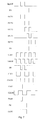
- FIG. 1 is a schematic structure diagram of a shift register unit according to a first embodiment of the present disclosure
- FIG. 2 is a schematic structure diagram of a shift register unit according to a second embodiment of the present disclosure
- FIG. 3 is a signal timing sequence diagram of the shift register unit in FIG. 2 ;
- FIG. 4 is a schematic structure diagram of a shift register unit according to a third embodiment of the present disclosure.
- FIG. 5 is a signal timing sequence diagram of the shift register unit in FIG. 4 ;
- FIG. 6 is a schematic structure diagram of a shift register according to another embodiment of the present disclosure.
- FIG. 7 is a signal timing sequence diagram of the shift register in FIG. 6 .
- the shift register unit provided by the embodiment of the present disclosure includes an input module P 1 , a reset module P 2 , a pull-down module P 3 , an output pull-down control module P 4 , and an output control module P 5 .
- the N-th stage shift register unit in the shift register will be described below.
- the input module P 1 has a control terminal connected to an input signal terminal Input N, an input terminal connected to a high level terminal VGH, and an output terminal connected to a pull-up control node PU, the pull-up control node PU being an intersection point of the input module P 1 , the reset module P 2 , the pull-down module P 3 , the pull-down control module P 4 and the output control module P 5 .
- the input module P 1 is used for outputting a pull-up control signal at the pull-up control node under control of a signal of the input signal terminal Input N.
- the reset module P 2 has a control terminal connected to the fifth stage output terminal OUT N+4, a first input terminal connected to the output terminal OUT N of the shift register unit, a second input terminal connected to the pull-up control node PU, and an output terminal connected to a low level terminal VGL, wherein the fifth-stage output terminal OUT N+4 is an output terminal of a corresponding fifth stage shift register unit in the cascaded shift register units in a case that the current shift register unit is used as a first stage shift register unit.
- the reset module P 2 is used for resetting the output terminal OUT N of the shift register unit and the pull-up control node.
- the pull-down module P 3 has a control terminal connected to a pull-down control node PD, a first input terminal connected to the output terminal OUT N of the shift register unit, a second input terminal connected to the pull-up control node PU, and an output terminal connected to the low level terminal VGL.
- the pull-down control node PD is an intersection point of the pull-down module P 3 and the output pull-down control module P 4 .
- the pull-down module P 3 is used for discharging the pull-up control node and the output terminal OUT N of the shift register unit.
- the output pull-down control module P 4 has a first control terminal connected to the pull-up control node PU, a second control terminal connected to the high level terminal VGH, a third control terminal connected to the output terminal OUT N of the shift register unit, a first input terminal connected to the low level terminal VGL, a first output terminal connected to the pull-down control node PD and a second output terminal connected to the output control node PB.
- the output control node PB is an intersection point of the output pull-down control module P 4 and the output control module P 5 .
- the output pull-down control module P 4 is used for generating and outputting a power supply enable signal and a power supply signal at the output control node PB.
- the output control module P 5 has a first control terminal connected to the pull-up control node PU, a first input terminal connected to a first clock signal terminal CL 1 , a first output terminal connected to the output terminal OUT N of the shift register unit, a second control terminal connected to the output terminal OUT N of the shift register unit, a second input terminal connected to the high level terminal VGH, a second output terminal connected to a gate drive signal terminal GATE, a third control terminal connected to a fourth stage output terminal OUT N+3, a third input terminal connected to the gate drive signal terminal GATE, a third output terminal connected to the low level terminal VGL, a fourth control terminal connected to a second clock signal terminal CL 2 , a fourth input terminal connected to the output control node PB, a fourth output terminal connected to a power supply signal terminal Elvdd, a fifth control terminal connected to a third clock signal terminal CL 3 , a fifth input terminal connected to the output control node PB, and a fifth output terminal connected to a power supply enable signal terminal
- the output control module P 5 is used for generating a gate drive signal and outputting the power supply enable signal at the power supply enable signal terminal EM, outputting the power supply signal at the power supply signal terminal Elvdd, and outputting the gate drive signal at the gate drive signal terminal GATE.
- the shift register unit provided by the embodiment of the present disclosure includes the input module P 1 , the reset module P 2 , the pull-down module P 3 , the output pull-down control module P 4 , and the output control module P 5 , wherein the output pull-down control module P 4 may provide the power supply enable signal and the power supply signal at the output control node PB, the output control module P 5 may generate the gate drive signal, receive the power supply enable signal and the power supply signal provided by the output pull-down control module, and output, at its output terminal, the three control signals, i.e., the power supply enable signal, the power supply signal and the gate drive signal.
- the shift register unit may provide three control signals, i.e., the power supply enable signal, the power supply signal and the gate drive signal, simultaneously for driving the pixel cell, and thus may reduce the number of the shift register units required in the shift register under the premise of the pixel cell being able to be driven, thereby simplifying the structure of the shift register and reducing the space occupied by the shift register.
- the driving method of the shift register unit as discussed above may comprise two phases:
- the input module P 1 receives the high level signal of the input signal terminal Input N, and charges the pull-up control node PU with the high level signal of the high-level terminal VGH;
- the output control module P 5 receives the high level signal of the pull-up control node PU and the signal of the first clock signal terminal CL 1 to provide a signal to the output terminal OUT N of the shift register unit, and outputs the gate drive signal at the gate drive signal terminal GATE based on the signal of the output terminal OUT N of the shift register unit and the signal of the fourth stage output terminal OUT N+3;
- the output pull-down control module P 4 receives the signal of the output terminal OUT N of the shift register unit and the high level signal of the high level terminal VGH to provide the power supply enable signal and the power supply signal at the output control node PB;
- the output control module P 5 receives the signal of the second clock signal terminal CL 2 and the signal of the third clock signal terminal CL 3 , and outputs the power supply enable signal and the power supply signal respectively at the
- the reset module P 2 receives the high level signal of the fifth stage output terminal OUT N+4, and resets the output terminal OUT N of the shift register unit and the pull-up control node PU to the low level signal;
- the output pull-down control module P 4 receives the low level signal of the pull-up control node PU, and provides the high level signal to the pull-down control node PD;
- the pull-down module P 3 receives the high level signal of the pull-down control node PD, and discharges the pull-up control node PU and the output terminal OUT N of the shift register unit;
- the output control module P 5 receives the low level signal of the pull-up control node PU and the signal of the fourth stage output terminal OUT N+3, and outputs the low level signal at the gate drive signal terminal GATE;
- the output pull-down control module P 4 receives the signal of the output terminal OUT N of the shift register unit and the high level signal of the high level terminal VGH to provide a high level signal at the output control node
- the above driving method is applied to the shift register unit in the foregoing embodiment.
- the driving method of the shift register unit has the same advantages as those of the shift register unit, and thus description thereof is omitted for simplicity.
- the input module P 1 comprises a first transistor T 1 , having a gate connected to the input signal terminal Input N, a source connected to the high level terminal VGH, and a drain connected to the pull-up control node PU.
- the gate of the first transistor T 1 corresponds to the control terminal of the input module
- the source of the first transistor T 1 corresponds to the input terminal of the input module
- the drain of the first transistor T 1 corresponds to the output terminal of the input module.
- the reset module P 2 comprises a second transistor T 2 and a third transistor T 3 ; wherein the second transistor T 2 has a gate connected to the fifth stage output terminal OUT N+4, a source connected to the output terminal OUT N of the shift register unit, and a drain connected to the low level terminal VGL; and the third transistor T 3 has a gate connected to the fifth stage output terminal OUT N+4, a source connected to the pull-up control node PU, and a drain connected to the low level terminal VGL.
- the gate of the second transistor T 2 and the gate of the third transistor T 3 correspond to the control terminal of the reset module
- the source of the second transistor T 2 corresponds to the first input terminal of the reset module
- the source of the third transistor T 3 corresponds to the second input terminal of the reset module
- the drain of the second transistor T 2 and the drain of the third transistor T 3 correspond to the output terminal of the reset module.
- the pull-down module P 3 comprises a fourth transistor T 4 and a fifth transistor T 5 , wherein the fourth transistor T 4 has a gate connected to the pull-down control node PD, a source connected to the output terminal OUT N of the shift register unit, and a drain connected to the low level terminal VGL; and the fifth transistor T 5 has a gate connected to the pull-down control node PD, a source connected to the pull-up control node PU, and a drain connected to the low-level terminal VGL.
- the gate of the fourth transistor T 4 and the gate of the fifth transistor T 5 correspond to the control terminal of the pull-down module
- the source of the fourth transistor T 4 corresponds to the first input terminal of the pull-down module
- the source of the fifth transistor T 5 corresponds to the second input terminal of the pull-down module
- the drain of the fourth transistor T 4 and the drain of the fifth transistor T 5 correspond to the output terminal of the pull-down module.
- the output pull-down control module P 4 comprises a sixth transistor T 6 , a seventh transistor T 7 , an eighth transistor T 8 , a ninth transistor T 9 and a tenth transistor T 10 , wherein the sixth transistor T 6 has a gate connected to the pull-up control node PU, a source connected to the pull-down control node PD, and a drain connected to the low level terminal VGL; the seventh transistor T 7 has a gate connected to a drain of the eighth transistor T 8 and a gate of the ninth transistor T 9 , a source connected to the high level terminal VGH, and a drain connected to the pull-down control node PD; the eighth transistor T 8 has a gate connected to the high level terminal VGH, a source connected to the high level terminal VGH, and the drain connected to the gate of the ninth transistor T 9 ; the ninth transistor T 9 has the gate connected to the gate of the seventh transistor T 7 , a source connected to the high level terminal VGH, and a drain connected to the output control node PB; and the
- the output control module P 5 comprises a first output control sub-module P 51 and a second output control sub-module P 52 , the first output control sub-module P 51 being configured to output the gate drive signal, and the second output control sub-module P 52 being configured to output the power supply enable signal and the power supply signal.
- the first output control sub-module P 51 comprises an eleventh transistor T 11 , a twelfth transistor T 12 and a thirteenth transistor T 13
- the second output control sub-module P 52 comprises a fourteenth transistor T 14 and a fifteenth transistor T 15
- the eleventh transistor T 11 has a gate connected to the pull-up control node PU, a source connected to the first clock signal terminal CL 1 , and a drain connected to the output terminal OUT N of the shift register unit
- the twelfth transistor T 12 has a gate connected to the output terminal OUT N of the shift register unit, a source connected to the high level terminal VGH, and a drain connected to the gate drive signal terminal GATE
- the thirteenth transistor T 13 has a gate connected to the fourth stage output terminal OUT N+3, a source connected to the gate drive signal terminal GATE, and a drain connected to the low level terminal VGL
- the fourteenth transistor T 14 has a gate connected to the second clock signal terminal CL 2 , a source connected to the eleventh
- the gate of the eleventh transistor corresponds to the first control terminal of the output control module P 5
- the source of the eleventh transistor corresponds to the first input terminal of the output control module P 5
- the drain of the eleventh transistor corresponds to the first output terminal of the output control module P 5
- the gate of the twelfth transistor corresponds to the second control terminal of the output control module P 5
- the source of the twelfth transistor corresponds to the second input terminal of the output control module P 5
- the drain of the twelfth transistor corresponds to the second output terminal of the output control module P 5
- the gate of the thirteenth transistor corresponds to the third control terminal of the output control module P 5
- the source of the thirteenth transistor corresponds to the third input terminal of the output control module P 5
- the drain of the thirteenth transistor corresponds to the third output terminal of the output control module P 5
- the gate of the fourteenth transistor corresponds to the fourth control terminal of the output control module P 5
- the source of the fourteenth transistor corresponds to the fourth control terminal of
- the source of the first transistor T 1 is connected to the source of the twelfth transistor T 12 ; and the drain of the first transistor T 1 is connected to the gate of the eleventh transistor T 11 , the source of the third transistor T 3 , the source of the fifth transistor T 5 , and the gate of the sixth transistor T 6 ; the source of the second transistor T 2 is connected to the drain of the eleventh transistor T 11 , the gate of the twelfth transistor T 12 , the source of the fourth transistor T 4 , and the gate of the tenth transistor T 10 ; and the drain of the second transistor T 2 is connected to the drain of the fourth transistor T 4 , the drain of the fifth transistor T 5 , the drain of the sixth transistor T 6 , the drain of the tenth transistor T 10 , and the drain of the thirteenth transistor T 13 ;
- the pull-up control node PU may particularly be an intersection point of the drain of the first transistor T 1 and the gate of the eleventh transistor T 11
- the pull-down control node PD may particularly be an intersection point of the source of the sixth transistor T 6 and the gate of the seventh transistor T 7
- the output control mode PB may particularly be an intersection point of the drain of the ninth transistor T 9 and the source of the tenth transistor T 10 .
- the respective transistors in the present embodiment are P-type transistors, which are only illustrated as an example. It should be noted that the respective transistors may also be N-type transistors, and a circuit design in which the transistors are N-type transistors also falls into the protection scope of the present disclosure.
- connections of the respective transistors are identical with those in the above embodiment, except that the connections of the respective input terminals and the output terminals are switched.
- the gate of the first transistor corresponds to the control terminal of the input module
- the drain of the first transistor corresponds to the input terminal of the input module
- the source of the first transistor corresponds to the output terminal of the input module.
- FIG. 3 shows a signal timing sequence diagram of the shift register unit as shown in FIG. 2 .
- the driving method of the shift register unit in the embodiment described in conjunction with FIG. 2 will be described with reference to FIG. 3 by taking P-type transistors as an example of the respective transistors.
- the first phase of the driving method of the shift register unit in the embodiment according to the present disclosure includes an A-B phase, a B-C phase, a C-D phase, a D-E phase and an E-F phase
- the second phase includes an F-G phase and a G-H phase.
- the signal of the input signal terminal Input N is a high level signal
- the gate of the first transistor T 1 receives the high level signal of the input signal terminal Input N
- the first transistor T 1 is turned on to charge the pull-up control node PU, and thus a signal of the pull-up control node PU is a high level signal
- the gate of the eleventh transistor T 11 receives the high level signal of the pull-up control node PU, the eleventh transistor T 11 is turned on, the signal of the first clock signal terminal CL 1 is a low level signal, the signal of the output terminal OUT N of the shift register unit is a low level signal, the twelfth transistor T 12 is turned off, and the signal of the gate drive signal terminal GATE is a low level signal
- the signal of the pull-up control node PU is a high level signal
- the sixth transistor T 6 is turned on
- the signal of the pull-down signal control node PD is a low level signal
- the signal of the input signal terminal Input N is a low level signal
- the first transistor T 1 is turned off, and the pull-up control node PU keeps the high level signal in the A-B phase
- the eleventh transistor T 11 is turned on, the signal of the first clock signal terminal CL 1 is a high-level signal
- the signal of the output terminal OUT N of the shift register unit is a high-level signal
- the gate of the twelfth transistor T 12 receives the high level signal of the high level terminal VGH through the twelfth transistor T 12 , and outputs the gate drive signal which is a high level signal
- the signal of the pull-up control node PU is a high level signal
- the sixth transistor T 6 is turned on, the signal of the pull-down control node PD is a low level signal
- the fourth transistor T 4 and the fifth transistor T 5 still remain in the turn-off state
- the gate of the tenth transistor T 10 receives the high level signal of the output terminal OUT N of the shift register unit
- the signal of the input signal terminal Input N is a high level signal
- the first transistor T 1 is turned on for charging the pull-up control node PU, the signal of the pull-up control node PU being a high level signal
- the eleventh transistor T 11 is turned on, the signal of the first clock signal terminal CL 1 is a low level signal
- the signal of the output terminal OUT N of the shift register unit is a low level signal
- the twelfth transistor T 12 is turned off, and the signal of the gate drive signal terminal GATE is kept as the high level signal in the B-C phase, i.e., the gate drive signal terminal GATE continues to output the gate drive signal
- the signal of the pull-up control node PU is a high level signal
- the sixth transistor T 6 is turned on, the signal of the pull-down control node PD is a low level signal
- both the fourth transistor T 4 and the fifth transistor T 5 are turned off
- the gate of the tenth transistor T 10 receives the low level signal of the output terminal
- the signal of the input signal terminal Input N is a low level signal
- the first transistor T 1 is turned off
- the pull-up control node PU keeps the high level signal in the C-D phase
- the eleventh transistor T 11 is turned on
- the signal of the first clock signal terminal CL 1 is a high level signal
- the signal of the output terminal OUT N of the shift register unit is a high level signal
- the gate of the twelfth transistor T 12 receives the high level signal of the output terminal OUT N of the shift register unit
- the twelfth transistor T 12 is turned on
- the gate drive signal terminal GATE receives the high level signal of the high level terminal VGH through the twelfth transistor T 12 , and outputs the gate drive signal, the gate drive signal being a high level signal
- the signal of the pull-up control node PU is a high level signal
- the sixth transistor T 6 is turned on
- the signal of the pull-down control node PD is a low level signal
- the signal of the input signal terminal Input N is a low level signal
- the first transistor T 1 is turned off
- the pull-up control node PU keeps the high level signal in the D-E phase
- the eleventh transistor T 11 is turned on
- the signal of the first clock signal terminal CL 1 is a low Level signal
- the signal of the output terminal OUT N of the shift register unit is a low level signal
- the twelfth transistor T 12 is turned off
- the signal of the fourth stage output terminal OUT N+3 is a high level signal
- the thirteenth transistor T 13 is turned on
- the signal of the gate drive signal terminal GATE is a low level signal
- the signal of the pull-up control node PU is a high level signal
- the sixth transistor T 6 is turned on
- the signal of the pull-down control node PD is a low level signal
- both the four transistors T 4 and the fifth transistor T 5 are turned off
- the gate of the tenth transistor T 10 receives the low level signal of the output terminal
- the signal of the input signal terminal Input N is a low level signal, and the first transistor T 1 is turned off; the signal of the fifth stage output terminal OUT N+4 is a high level signal, both the second transistor T 2 and the third transistor T 3 are turned on, the output terminal OUT N of the shift register unit is discharged by the second transistor T 2 , the output terminal OUT N of the shift register unit is reset to the low level signal, the pull-up control node PU is discharged by the third transistor T 3 , the pull-up control node PU is reset to the low-level signal; the gate of the sixth transistor T 6 receives the low-level signal of the pull-up control node PU, the sixth transistor T 6 is turned off, and thus the signal of the pull-down control node PD is a high level signal; the gate of the fourth transistor T 4 and the gate of the fifth transistor T 5 receive the high level signal of the pull-down control node PD, both the fourth transistor T 4 and the fifth transistor T 5 are turned on, the
- the signal of the input signal terminal Input N is a low level signal, and the first transistor T 1 is turned off;
- the signal of the fifth stage output terminal OUT N+4 is a low level signal, both the second transistor T 2 and the third transistor T 3 are turned off, the output terminal OUT N of the shift register unit keeps the low level signal in the F-G phase, and the pull-up control node PU keeps the low level signal in the F-G phase;
- the gate of the sixth transistor T 6 receives the low level signal of the pull-up control node PU, the sixth transistor T 6 is turned off, and thus the signal of the pull-down control signal PD is a high level signal;
- the gate of the fourth transistor T 4 and the gate of the fifth transistor T 5 receive the high level signal of the pull-down control node PD, both the fourth transistor T 4 and the fifth transistor T 5 are turned on, the fourth transistor T 4 further discharges the output terminal OUT N of the shift register unit, and the fifth transistor T 5 further discharges the pull-up control node
- the seventh transistor T 7 , the eighth transistor T 8 and the ninth transistor T 9 are all kept turn-on, wherein the output of the eighth transistor T 8 is high, controlling the seventh transistor T 7 and the ninth transistor T 9 to be turned on, thereby writing the high level signals in the PD node and the PB node respectively.
- FIG. 2 shows that both the gate and the source of the eighth transistor T 8 are connected to the high level terminal VGH, they may be connected to the inverted signal of the first clock signal CL 1 to ensure that the PU node becomes high before the PU node, so that the PD node may be discharged by the PU node when the PU node is high.
- the signal of the second clock signal terminal CL 2 and the signal of the third clock signal terminal CL 3 are mutually inverted signals, and a frequency of the signal of the first clock signal terminal CL 1 is different from a frequency of the signal of the second clock signal terminal CL 2 .
- the frequency of the signal of the first clock signal terminal CL 1 is twice the frequency of the signal of the second clock signal terminal CL 2 .
- the present disclosure further provides a shift register, which comprises multiple stages of the shift register units as previously described in the embodiments according to the present disclosure, wherein the output terminal of a previous stage of shift register unit is connected to an input signal terminal of a next stage of shift register unit.
- a current output terminal OUT 1 of the first stage of shift register unit UNIT 1 is connected to an input signal terminal Input 2 of the second stage of shift register unit UNIT 2 , as shown in FIG. 4 .
- the shift register comprises N stages of the shift register units as previously described in the embodiments according to the present disclosure, N being an integer no less than 4; wherein both the first clock signal terminal CL 1 of an i-th stage shift register unit and the first clock signal terminal CL 1 of an (i+2)-th stage shift register unit input the first clock signal, and both the first clock signal terminal CL 1 of an (i+1)-th stage shift register unit and the first clock signal terminal CL 1 of an (i+3)-th stage shift register unit input the inverted signal of the first clock signal; both the second clock signal terminal CL 2 of the i-th stage shift register unit and the second clock signal terminal of the (i+1)-th stage shift register unit input the second clock signal, and both the second clock signal terminal of the (i+2)-th stage shift register unit and the second clock signal terminal of the (i+3)-th stage shift register unit input the inverted signal of the second clock signal; and both the third clock signal terminal of the i-th stage shift register unit and the third clock signal terminal of the (i+1)-th stage
- a first clock signal terminal CL 1 of the first stage of shift register unit UNIT 1 inputs a first clock signal CLK 1
- a second clock signal terminal CL 2 inputs a second clock signal CLK 2
- a third clock signal terminal CL 3 inputs an inverted signal CLK 2 B of the second clock signal
- a first reset terminal Reset 11 is connected to an output terminal OUT 4 of the fourth stage of shift register unit
- a second reset terminal Reset 12 is connected to an output terminal OUT 5 of the fifth stage of shift register unit
- a first clock signal terminal CL 1 of the second stage of shift register unit UNIT 2 inputs an inverted signal CLK 1 B of the first clock signal
- a second clock signal terminal CL 2 inputs the second clock signal CLK 2
- a third clock signal terminal CL 3 inputs the inverted signal CLK 2 B of the second clock signal
- a first reset terminal Reset 21 is connected to the output terminal OUT 5 of the fifth stage of shift register unit
- a second reset terminal Reset 22 is connected to
- the gate drive signals, the power supply enable signals and the power supply signals output by the respective stages of shift register units are used for driving corresponding rows of pixel cells. That is, the gate drive signal terminal, the power supply enable signal terminal and the power supply power terminal of each stage of shift register unit are connected to terminals of the corresponding pixel cell.
- shift register units in the shift register have the same advantages as those of the shift register unit in the above embodiments, and thus description thereof is omitted for simplicity.
- FIG. 5 shows a signal timing sequence diagram of the shift register in the embodiment according to the present disclosure.
- a particular driving method of the shift register may refer to the driving method of the shift register units which constitute the shift register. Illustration of the signal timing sequence diagram in FIG. 5 may also refer to that of the signal timing sequence diagram in FIG. 3 .
- a third clock signal which has a hysteresis with respect to the second clock signal (e.g., is delayed by a half of a clock cycle with respect to the second clock signal), may be provided in order to ensure the timings of driving the respective shift register units.
- both the first clock signal terminal CL 1 of the i-th stage shift register unit and the first clock signal terminal CL 1 of the (i+2)-th stage shift register unit input the first clock signal
- both the first clock signal terminal CL 1 of the (i+1)-th stage shift register unit and the first clock signal terminal CL 1 of the (i+3)-th stage shift register unit input the inverted signal of the first clock signal
- the second clock signal terminal CL 2 of the i-th stage shift register unit inputs the second clock signal
- the second clock signal terminal CL 2 of the (i+1)-th stage shift register unit inputs the third clock signal
- the second clock signal terminal CL 2 of the (i+2)-th stage shift register unit inputs the inverted signal of the second clock signal
- the second clock signal terminal of the (i+3)-th stage shift register unit inputs the inverted signal of the second clock signal
- the third clock signal terminal CL 3 of the i-th stage shift register unit inputs the inverted signal of the
- a first clock signal terminal CL 1 of the first stage of shift register unit UNIT 1 inputs a first clock signal CLK 1
- a second clock signal terminal CL 2 inputs a second clock signal CLK 2
- a third clock signal terminal CL 3 inputs an inverted signal CLK 2 B of the second clock signal
- a first reset terminal Reset 11 is connected to an output terminal OUT 4 of the fourth stage of shift register unit
- a second reset terminal Reset 12 is connected to an output terminal OUT 5 of the fifth stage of shift register unit
- a first clock signal terminal CL 1 of the second stage of shift register unit UNIT 2 inputs an inverted signal CLK 1 B of the first clock signal
- a second clock signal terminal CL 2 inputs the third clock signal CLK 3
- a third clock signal terminal CL 3 inputs an inverted signal CLK 3 B of the third clock signal
- a first reset terminal Reset 21 is connected to the output terminal OUT 5 of the fifth stage of shift register unit
- a second reset terminal Reset 22 is connected to
- FIG. 7 shows a signal timing sequence diagram of the shift register in the present embodiment.
- a particular driving method of the shift register may refer to the driving method of the shift register units which constitute the shift register. Illustration of the signal timing sequence diagram in FIG. 7 may also refer to that of the signal timing sequence diagram in FIG. 3 .
- the present disclosure further provides a display device.
- the display device comprises the shift register in the above third embodiment, wherein the power supply enable signal, the power supply signal and the gate drive signal provided by the shift register unit in the shift register are used for driving the pixel cells in the display device.
- the shift register in the display device has the same advantages as that in the above embodiments, and thus description thereof is omitted for simplicity.
- the display device may be an organic light-emitting diode display panel, an e-paper, a mobile phone, a tablet, a TV, a display, a notebook, a digital photo frame, a navigator, and any other products or components having a display function.
Landscapes
- Engineering & Computer Science (AREA)
- Physics & Mathematics (AREA)
- Computer Hardware Design (AREA)
- General Physics & Mathematics (AREA)
- Theoretical Computer Science (AREA)
- Chemical & Material Sciences (AREA)
- Crystallography & Structural Chemistry (AREA)
- Shift Register Type Memory (AREA)
- Control Of Indicators Other Than Cathode Ray Tubes (AREA)
- Liquid Crystal Display Device Control (AREA)
Abstract
Description
Claims (20)
Applications Claiming Priority (4)
| Application Number | Priority Date | Filing Date | Title |
|---|---|---|---|
| CN201510353895.1A CN104867438B (en) | 2015-06-24 | 2015-06-24 | Shift register cell and its driving method, shift register and display device |
| CN201510353895.1 | 2015-06-24 | ||
| CN201510353895 | 2015-06-24 | ||
| PCT/CN2015/092003 WO2016206240A1 (en) | 2015-06-24 | 2015-10-15 | Shift register unit and drive method thereof, shift register and display device |
Publications (2)
| Publication Number | Publication Date |
|---|---|
| US20170309211A1 US20170309211A1 (en) | 2017-10-26 |
| US9965986B2 true US9965986B2 (en) | 2018-05-08 |
Family
ID=53913238
Family Applications (1)
| Application Number | Title | Priority Date | Filing Date |
|---|---|---|---|
| US15/517,587 Active US9965986B2 (en) | 2015-06-24 | 2015-10-15 | Shift register unit and driving method thereof, shift register and display device |
Country Status (3)
| Country | Link |
|---|---|
| US (1) | US9965986B2 (en) |
| CN (1) | CN104867438B (en) |
| WO (1) | WO2016206240A1 (en) |
Families Citing this family (17)
| Publication number | Priority date | Publication date | Assignee | Title |
|---|---|---|---|---|
| CN104867438B (en) * | 2015-06-24 | 2018-02-13 | 合肥鑫晟光电科技有限公司 | Shift register cell and its driving method, shift register and display device |
| CN105632560B (en) * | 2016-01-04 | 2019-08-02 | 京东方科技集团股份有限公司 | Shift register unit, driving method, gate driving circuit and display device |
| CN105788508B (en) * | 2016-05-24 | 2017-07-25 | 京东方科技集团股份有限公司 | A gate drive circuit and display panel |
| CN106205461B (en) * | 2016-09-30 | 2019-04-02 | 京东方科技集团股份有限公司 | Shift register unit, driving method, gate driving circuit and display device |
| CN106251804B (en) * | 2016-09-30 | 2018-12-21 | 京东方科技集团股份有限公司 | Shift register cell, driving method, gate driving circuit and display device |
| CN109147635B (en) * | 2017-06-27 | 2021-04-16 | 上海天马有机发光显示技术有限公司 | A shift register, its driving method and display device |
| CN108257574B (en) * | 2018-03-23 | 2020-07-21 | 京东方科技集团股份有限公司 | Pixel circuit, array substrate, driving method thereof and related device |
| CN108511025B (en) * | 2018-04-12 | 2020-06-16 | 京东方科技集团股份有限公司 | A shift register unit, gate drive circuit and display device |
| CN109686292B (en) * | 2019-01-25 | 2022-05-27 | 鄂尔多斯市源盛光电有限责任公司 | Gate driving unit, gate driving method, gate driving circuit and display device |
| CN110007628B (en) * | 2019-04-10 | 2022-02-01 | 深圳市华星光电半导体显示技术有限公司 | GOA circuit and display panel |
| CN110070822A (en) * | 2019-06-12 | 2019-07-30 | 京东方科技集团股份有限公司 | A kind of shift register cell and its driving method, gate driving circuit |
| CN110767256B (en) * | 2019-11-11 | 2024-10-22 | 合肥京东方卓印科技有限公司 | Shift register unit and driving method thereof, gate driving circuit and display device |
| CN111145823B (en) * | 2019-12-25 | 2022-04-05 | 武汉天马微电子有限公司 | Shift register, gate driving circuit, display panel and display device |
| CN111477181B (en) | 2020-05-22 | 2021-08-27 | 京东方科技集团股份有限公司 | Gate driving circuit, display substrate, display device and gate driving method |
| US12062311B2 (en) * | 2021-08-30 | 2024-08-13 | Boe Technology Group Co., Ltd. | Display panel, method for driving shift register unit thereof, and shift register |
| CN114465617B (en) * | 2021-12-30 | 2022-12-09 | 北京奕斯伟计算技术股份有限公司 | Level shift circuit, integrated circuit, and electronic device |
| CN115206239B (en) * | 2022-06-30 | 2024-09-24 | 厦门天马显示科技有限公司 | Display panel, display driving method and display device |
Citations (12)
| Publication number | Priority date | Publication date | Assignee | Title |
|---|---|---|---|---|
| US20100260312A1 (en) | 2009-04-08 | 2010-10-14 | Tsung-Ting Tsai | Shift register of lcd devices |
| US20110316831A1 (en) | 2010-06-23 | 2011-12-29 | Panasonic Liquid Crystal Display Co., Ltd. | Bidirectional shift register and image display device using the same |
| CN102915698A (en) | 2012-10-18 | 2013-02-06 | 京东方科技集团股份有限公司 | Shifting register unit, grid electrode drive circuit and display device |
| CN103208262A (en) | 2012-01-12 | 2013-07-17 | 三星电子株式会社 | Gate driver and display apparatus having the same |
| CN103280198A (en) | 2013-02-06 | 2013-09-04 | 友达光电股份有限公司 | Display panel and gate driver thereof |
| CN104409102A (en) | 2014-10-31 | 2015-03-11 | 友达光电股份有限公司 | Shift register |
| CN104464600A (en) | 2014-12-26 | 2015-03-25 | 合肥鑫晟光电科技有限公司 | Shifting register unit, driving method of shifting register unit, shifting register circuit and display device |
| CN104867438A (en) | 2015-06-24 | 2015-08-26 | 合肥鑫晟光电科技有限公司 | Shift register unit and driving method thereof, shift register and display device |
| US20160321999A1 (en) * | 2013-12-30 | 2016-11-03 | Kunshan New Flat Panel Display Techn. Center Co. | Scanning Drive Circuit and Organic Light-Emitting Display |
| US20160329015A1 (en) * | 2014-11-20 | 2016-11-10 | Boe Technology Group Co., Ltd. | Shift register unit and method for driving the same, shift register and display apparatus |
| US20170193887A1 (en) * | 2016-01-05 | 2017-07-06 | Boe Technology Group Co., Ltd. | Shift register, a gate line driving circuit, an array substrate and a display apparatus |
| US20170193961A1 (en) * | 2016-01-04 | 2017-07-06 | Boe Technology Group Co., Ltd. | Shift register unit, its driving method, gate driver circuit and display device |
-
2015
- 2015-06-24 CN CN201510353895.1A patent/CN104867438B/en active Active
- 2015-10-15 WO PCT/CN2015/092003 patent/WO2016206240A1/en not_active Ceased
- 2015-10-15 US US15/517,587 patent/US9965986B2/en active Active
Patent Citations (15)
| Publication number | Priority date | Publication date | Assignee | Title |
|---|---|---|---|---|
| US20100260312A1 (en) | 2009-04-08 | 2010-10-14 | Tsung-Ting Tsai | Shift register of lcd devices |
| US20110316831A1 (en) | 2010-06-23 | 2011-12-29 | Panasonic Liquid Crystal Display Co., Ltd. | Bidirectional shift register and image display device using the same |
| US8816728B2 (en) | 2012-01-12 | 2014-08-26 | Samsung Display Co., Ltd. | Gate driving circuit and display apparatus having the same |
| CN103208262A (en) | 2012-01-12 | 2013-07-17 | 三星电子株式会社 | Gate driver and display apparatus having the same |
| US8587347B2 (en) | 2012-01-12 | 2013-11-19 | Samsung Display Co., Ltd. | Gate driving circuit and display apparatus having the same |
| CN102915698A (en) | 2012-10-18 | 2013-02-06 | 京东方科技集团股份有限公司 | Shifting register unit, grid electrode drive circuit and display device |
| CN103280198A (en) | 2013-02-06 | 2013-09-04 | 友达光电股份有限公司 | Display panel and gate driver thereof |
| US20160321999A1 (en) * | 2013-12-30 | 2016-11-03 | Kunshan New Flat Panel Display Techn. Center Co. | Scanning Drive Circuit and Organic Light-Emitting Display |
| CN104409102A (en) | 2014-10-31 | 2015-03-11 | 友达光电股份有限公司 | Shift register |
| US20160329015A1 (en) * | 2014-11-20 | 2016-11-10 | Boe Technology Group Co., Ltd. | Shift register unit and method for driving the same, shift register and display apparatus |
| CN104464600A (en) | 2014-12-26 | 2015-03-25 | 合肥鑫晟光电科技有限公司 | Shifting register unit, driving method of shifting register unit, shifting register circuit and display device |
| US20160351159A1 (en) | 2014-12-26 | 2016-12-01 | Boe Technology Group Co., Ltd. | Shift register unit and method for driving same, shift register circuit and display apparatus |
| CN104867438A (en) | 2015-06-24 | 2015-08-26 | 合肥鑫晟光电科技有限公司 | Shift register unit and driving method thereof, shift register and display device |
| US20170193961A1 (en) * | 2016-01-04 | 2017-07-06 | Boe Technology Group Co., Ltd. | Shift register unit, its driving method, gate driver circuit and display device |
| US20170193887A1 (en) * | 2016-01-05 | 2017-07-06 | Boe Technology Group Co., Ltd. | Shift register, a gate line driving circuit, an array substrate and a display apparatus |
Non-Patent Citations (5)
| Title |
|---|
| English translation of Box No. V of the Written Opinion for the International Searching Authority for International Application No. PCT/CN2015/092003, 2 pages. |
| English translation of Written Opinion of the International Searching Authority for International Application No. PCT/CN2015/092003, dated Apr. 1, 2016, 7 pages. |
| First Office Action from Chinese Patent Application No. 201510353895.1, dated Jan. 22, 2017, 10 pages. |
| International Search Report and Written Opinion of International Application No. PCT/CN2015/092003, dated Apr. 1, 2016, 8 pages. |
| Second Office Action from Chinese Patent Application No. 201510353895.1, dated Jul. 17, 2017, 5 pages. |
Also Published As
| Publication number | Publication date |
|---|---|
| WO2016206240A1 (en) | 2016-12-29 |
| US20170309211A1 (en) | 2017-10-26 |
| CN104867438B (en) | 2018-02-13 |
| CN104867438A (en) | 2015-08-26 |
Similar Documents
| Publication | Publication Date | Title |
|---|---|---|
| US9965986B2 (en) | Shift register unit and driving method thereof, shift register and display device | |
| US11127478B2 (en) | Shift register unit and driving method thereof, gate driving circuit, and display device | |
| US9847067B2 (en) | Shift register, gate driving circuit, display panel, driving method thereof and display device | |
| US11282470B2 (en) | Shift register element, method for driving the same, gate driver circuit, and display device | |
| US9747854B2 (en) | Shift register, gate driving circuit, method for driving display panel and display device | |
| US9530521B2 (en) | Shift register unit, gate driving circuit, and display device | |
| US10657879B1 (en) | Gate driving circuit, method for driving the same, and display apparatus | |
| EP2991077B1 (en) | Shift register unit and display device | |
| CN108182905B (en) | Switching circuit, control unit, display device, gate driving circuit and method | |
| US11355068B2 (en) | Shift register unit, gate drive circuit and drive method | |
| US20150325190A1 (en) | Shift register unit, gate driving circuit and display device | |
| EP3882901B1 (en) | Shift register unit, drive method, gate drive circuit, and display device | |
| US11094389B2 (en) | Shift register unit and driving method, gate driving circuit, and display device | |
| US9299452B2 (en) | Shift registers, display panels, display devices, and electronic devices | |
| CN105575318B (en) | A display panel and display device | |
| US10872546B2 (en) | Shift register unit and method for driving the same, gate driving circuit and display apparatus | |
| CN108281124A (en) | Shift register cell and its driving method, gate driving circuit and display device | |
| US10706947B2 (en) | Shift register unit and driving method thereof, gate driving circuit, and display device | |
| US10580380B2 (en) | Level conversion circuit, display apparatus, and driving method | |
| US11423823B2 (en) | Shift register and driving method thereof, gate driving circuit and display device capabling reset the output terminal | |
| WO2020168895A1 (en) | Shift register unit and method for driving same, gate driver, touch control display panel, and touch control display apparatus | |
| US20180218688A1 (en) | Shift register, gate driving circuit, array substrate | |
| US10997890B2 (en) | Shift register, a gate driver circuit and a display device | |
| US11640795B2 (en) | Shift register unit, gate drive circuit and drive method | |
| US10553140B2 (en) | Inversion control circuit, method for driving the same, display panel, and display device |
Legal Events
| Date | Code | Title | Description |
|---|---|---|---|
| AS | Assignment |
Owner name: HEFEI XINSHENG OPTOELECTRONICS TECHNOLOGY CO., LTD Free format text: ASSIGNMENT OF ASSIGNORS INTEREST;ASSIGNOR:ZHANG, YUTING;REEL/FRAME:041928/0156 Effective date: 20170329 Owner name: BOE TECHNOLOGY GROUP CO., LTD., CHINA Free format text: ASSIGNMENT OF ASSIGNORS INTEREST;ASSIGNOR:ZHANG, YUTING;REEL/FRAME:041928/0156 Effective date: 20170329 |
|
| STCF | Information on status: patent grant |
Free format text: PATENTED CASE |
|
| MAFP | Maintenance fee payment |
Free format text: PAYMENT OF MAINTENANCE FEE, 4TH YEAR, LARGE ENTITY (ORIGINAL EVENT CODE: M1551); ENTITY STATUS OF PATENT OWNER: LARGE ENTITY Year of fee payment: 4 |
|
| MAFP | Maintenance fee payment |
Free format text: PAYMENT OF MAINTENANCE FEE, 8TH YEAR, LARGE ENTITY (ORIGINAL EVENT CODE: M1552); ENTITY STATUS OF PATENT OWNER: LARGE ENTITY Year of fee payment: 8 |