US9964806B2 - Display device - Google Patents
Display device Download PDFInfo
- Publication number
- US9964806B2 US9964806B2 US15/229,706 US201615229706A US9964806B2 US 9964806 B2 US9964806 B2 US 9964806B2 US 201615229706 A US201615229706 A US 201615229706A US 9964806 B2 US9964806 B2 US 9964806B2
- Authority
- US
- United States
- Prior art keywords
- color
- liquid crystal
- display device
- substrate
- disposed
- Prior art date
- Legal status (The legal status is an assumption and is not a legal conclusion. Google has not performed a legal analysis and makes no representation as to the accuracy of the status listed.)
- Active, expires
Links
- 239000004973 liquid crystal related substance Substances 0.000 claims abstract description 203
- 239000000758 substrate Substances 0.000 claims abstract description 97
- 239000010410 layer Substances 0.000 claims description 254
- 239000000975 dye Substances 0.000 claims description 119
- 239000002245 particle Substances 0.000 claims description 31
- 238000000149 argon plasma sintering Methods 0.000 claims description 12
- 239000001000 anthraquinone dye Substances 0.000 claims description 8
- 239000011229 interlayer Substances 0.000 claims description 7
- 239000002019 doping agent Substances 0.000 claims description 6
- 239000004988 Nematic liquid crystal Substances 0.000 claims 1
- 239000002096 quantum dot Substances 0.000 description 53
- 230000005684 electric field Effects 0.000 description 43
- 239000000463 material Substances 0.000 description 29
- 238000002834 transmittance Methods 0.000 description 28
- 230000010287 polarization Effects 0.000 description 27
- 238000002835 absorbance Methods 0.000 description 15
- 230000003287 optical effect Effects 0.000 description 10
- XLOMVQKBTHCTTD-UHFFFAOYSA-N Zinc monoxide Chemical compound [Zn]=O XLOMVQKBTHCTTD-UHFFFAOYSA-N 0.000 description 8
- 238000004519 manufacturing process Methods 0.000 description 7
- 230000007704 transition Effects 0.000 description 7
- MDPQAAIBOYKPTH-UHFFFAOYSA-N CC(C)(C)c1ccc(Sc2cccc3c2C(=O)c2cccc(Sc4ccc5ccccc5c4)c2C3=O)cc1.CC(C)(C)c1ccc(Sc2cccc3c2C(=O)c2cccc(Sc4ccccc4)c2C3=O)cc1.O=C1c2cccc(Sc3ccc4ccccc4c3)c2C(=O)c2cccc(Sc3ccc4ccccc4c3)c21.O=C1c2cccc(Sc3ccccc3)c2C(=O)c2cccc(Sc3ccccc3)c21 Chemical compound CC(C)(C)c1ccc(Sc2cccc3c2C(=O)c2cccc(Sc4ccc5ccccc5c4)c2C3=O)cc1.CC(C)(C)c1ccc(Sc2cccc3c2C(=O)c2cccc(Sc4ccccc4)c2C3=O)cc1.O=C1c2cccc(Sc3ccc4ccccc4c3)c2C(=O)c2cccc(Sc3ccc4ccccc4c3)c21.O=C1c2cccc(Sc3ccccc3)c2C(=O)c2cccc(Sc3ccccc3)c21 MDPQAAIBOYKPTH-UHFFFAOYSA-N 0.000 description 5
- 230000007547 defect Effects 0.000 description 5
- 239000000203 mixture Substances 0.000 description 5
- 239000004065 semiconductor Substances 0.000 description 5
- 230000005540 biological transmission Effects 0.000 description 4
- 150000001875 compounds Chemical class 0.000 description 4
- 230000001105 regulatory effect Effects 0.000 description 4
- 230000004044 response Effects 0.000 description 4
- 239000011787 zinc oxide Substances 0.000 description 4
- 230000000903 blocking effect Effects 0.000 description 3
- 230000001276 controlling effect Effects 0.000 description 3
- 238000005259 measurement Methods 0.000 description 3
- -1 polysiloxane Polymers 0.000 description 3
- 239000011347 resin Substances 0.000 description 3
- 229920005989 resin Polymers 0.000 description 3
- 229910052984 zinc sulfide Inorganic materials 0.000 description 3
- 229910004613 CdTe Inorganic materials 0.000 description 2
- 229910004262 HgTe Inorganic materials 0.000 description 2
- 239000004642 Polyimide Substances 0.000 description 2
- PPBRXRYQALVLMV-UHFFFAOYSA-N Styrene Chemical compound C=CC1=CC=CC=C1 PPBRXRYQALVLMV-UHFFFAOYSA-N 0.000 description 2
- 229910007709 ZnTe Inorganic materials 0.000 description 2
- 238000007792 addition Methods 0.000 description 2
- 230000008901 benefit Effects 0.000 description 2
- UHYPYGJEEGLRJD-UHFFFAOYSA-N cadmium(2+);selenium(2-) Chemical compound [Se-2].[Cd+2] UHYPYGJEEGLRJD-UHFFFAOYSA-N 0.000 description 2
- 239000003086 colorant Substances 0.000 description 2
- 239000004020 conductor Substances 0.000 description 2
- ZYGHJZDHTFUPRJ-UHFFFAOYSA-N coumarin Chemical compound C1=CC=C2OC(=O)C=CC2=C1 ZYGHJZDHTFUPRJ-UHFFFAOYSA-N 0.000 description 2
- 230000007423 decrease Effects 0.000 description 2
- 238000009792 diffusion process Methods 0.000 description 2
- 239000011521 glass Substances 0.000 description 2
- 239000011159 matrix material Substances 0.000 description 2
- 238000000034 method Methods 0.000 description 2
- 239000002159 nanocrystal Substances 0.000 description 2
- 239000011368 organic material Substances 0.000 description 2
- 239000011146 organic particle Substances 0.000 description 2
- 229920003023 plastic Polymers 0.000 description 2
- 229920005575 poly(amic acid) Polymers 0.000 description 2
- 229920003229 poly(methyl methacrylate) Polymers 0.000 description 2
- 229920001721 polyimide Polymers 0.000 description 2
- 239000004926 polymethyl methacrylate Substances 0.000 description 2
- 229920001296 polysiloxane Polymers 0.000 description 2
- SBIBMFFZSBJNJF-UHFFFAOYSA-N selenium;zinc Chemical compound [Se]=[Zn] SBIBMFFZSBJNJF-UHFFFAOYSA-N 0.000 description 2
- 229910052950 sphalerite Inorganic materials 0.000 description 2
- 239000012780 transparent material Substances 0.000 description 2
- MFEVGQHCNVXMER-UHFFFAOYSA-L 1,3,2$l^{2}-dioxaplumbetan-4-one Chemical compound [Pb+2].[O-]C([O-])=O MFEVGQHCNVXMER-UHFFFAOYSA-L 0.000 description 1
- TZMSYXZUNZXBOL-UHFFFAOYSA-N 10H-phenoxazine Chemical compound C1=CC=C2NC3=CC=CC=C3OC2=C1 TZMSYXZUNZXBOL-UHFFFAOYSA-N 0.000 description 1
- GZVHEAJQGPRDLQ-UHFFFAOYSA-N 6-phenyl-1,3,5-triazine-2,4-diamine Chemical compound NC1=NC(N)=NC(C=2C=CC=CC=2)=N1 GZVHEAJQGPRDLQ-UHFFFAOYSA-N 0.000 description 1
- 239000004925 Acrylic resin Substances 0.000 description 1
- 229920000178 Acrylic resin Polymers 0.000 description 1
- BULRPDFNLCXRQD-UHFFFAOYSA-N Cc1ccc2c(c1)OC(=O)C(/C1=N/c3ccccc3S1)=C2 Chemical compound Cc1ccc2c(c1)OC(=O)C(/C1=N/c3ccccc3S1)=C2 BULRPDFNLCXRQD-UHFFFAOYSA-N 0.000 description 1
- 229910016423 CuZnS Inorganic materials 0.000 description 1
- 229910002601 GaN Inorganic materials 0.000 description 1
- 229910005540 GaP Inorganic materials 0.000 description 1
- 229910000003 Lead carbonate Inorganic materials 0.000 description 1
- 239000004677 Nylon Substances 0.000 description 1
- 239000004698 Polyethylene Substances 0.000 description 1
- VYPSYNLAJGMNEJ-UHFFFAOYSA-N Silicium dioxide Chemical compound O=[Si]=O VYPSYNLAJGMNEJ-UHFFFAOYSA-N 0.000 description 1
- XUIMIQQOPSSXEZ-UHFFFAOYSA-N Silicon Chemical compound [Si] XUIMIQQOPSSXEZ-UHFFFAOYSA-N 0.000 description 1
- GWEVSGVZZGPLCZ-UHFFFAOYSA-N Titan oxide Chemical compound O=[Ti]=O GWEVSGVZZGPLCZ-UHFFFAOYSA-N 0.000 description 1
- 239000005083 Zinc sulfide Substances 0.000 description 1
- 239000011358 absorbing material Substances 0.000 description 1
- 238000010521 absorption reaction Methods 0.000 description 1
- 239000012790 adhesive layer Substances 0.000 description 1
- 229910000410 antimony oxide Inorganic materials 0.000 description 1
- 239000000987 azo dye Substances 0.000 description 1
- 230000008859 change Effects 0.000 description 1
- 229910052956 cinnabar Inorganic materials 0.000 description 1
- 229960000956 coumarin Drugs 0.000 description 1
- 235000001671 coumarin Nutrition 0.000 description 1
- 229910003460 diamond Inorganic materials 0.000 description 1
- 239000010432 diamond Substances 0.000 description 1
- 230000000694 effects Effects 0.000 description 1
- 238000001914 filtration Methods 0.000 description 1
- COHYTHOBJLSHDF-BUHFOSPRSA-N indigo dye Chemical compound N\1C2=CC=CC=C2C(=O)C/1=C1/C(=O)C2=CC=CC=C2N1 COHYTHOBJLSHDF-BUHFOSPRSA-N 0.000 description 1
- COHYTHOBJLSHDF-UHFFFAOYSA-N indigo powder Natural products N1C2=CC=CC=C2C(=O)C1=C1C(=O)C2=CC=CC=C2N1 COHYTHOBJLSHDF-UHFFFAOYSA-N 0.000 description 1
- AMGQUBHHOARCQH-UHFFFAOYSA-N indium;oxotin Chemical compound [In].[Sn]=O AMGQUBHHOARCQH-UHFFFAOYSA-N 0.000 description 1
- 239000010954 inorganic particle Substances 0.000 description 1
- 229910000464 lead oxide Inorganic materials 0.000 description 1
- DZVCFNFOPIZQKX-LTHRDKTGSA-M merocyanine Chemical compound [Na+].O=C1N(CCCC)C(=O)N(CCCC)C(=O)C1=C\C=C\C=C/1N(CCCS([O-])(=O)=O)C2=CC=CC=C2O\1 DZVCFNFOPIZQKX-LTHRDKTGSA-M 0.000 description 1
- 229910052751 metal Inorganic materials 0.000 description 1
- 239000002184 metal Substances 0.000 description 1
- 238000012986 modification Methods 0.000 description 1
- 230000004048 modification Effects 0.000 description 1
- AJDUTMFFZHIJEM-UHFFFAOYSA-N n-(9,10-dioxoanthracen-1-yl)-4-[4-[[4-[4-[(9,10-dioxoanthracen-1-yl)carbamoyl]phenyl]phenyl]diazenyl]phenyl]benzamide Chemical compound O=C1C2=CC=CC=C2C(=O)C2=C1C=CC=C2NC(=O)C(C=C1)=CC=C1C(C=C1)=CC=C1N=NC(C=C1)=CC=C1C(C=C1)=CC=C1C(=O)NC1=CC=CC2=C1C(=O)C1=CC=CC=C1C2=O AJDUTMFFZHIJEM-UHFFFAOYSA-N 0.000 description 1
- 239000002086 nanomaterial Substances 0.000 description 1
- 229920001778 nylon Polymers 0.000 description 1
- 239000011242 organic-inorganic particle Substances 0.000 description 1
- TWNQGVIAIRXVLR-UHFFFAOYSA-N oxo(oxoalumanyloxy)alumane Chemical compound O=[Al]O[Al]=O TWNQGVIAIRXVLR-UHFFFAOYSA-N 0.000 description 1
- VTRUBDSFZJNXHI-UHFFFAOYSA-N oxoantimony Chemical compound [Sb]=O VTRUBDSFZJNXHI-UHFFFAOYSA-N 0.000 description 1
- YEXPOXQUZXUXJW-UHFFFAOYSA-N oxolead Chemical compound [Pb]=O YEXPOXQUZXUXJW-UHFFFAOYSA-N 0.000 description 1
- RVTZCBVAJQQJTK-UHFFFAOYSA-N oxygen(2-);zirconium(4+) Chemical compound [O-2].[O-2].[Zr+4] RVTZCBVAJQQJTK-UHFFFAOYSA-N 0.000 description 1
- 125000002080 perylenyl group Chemical group C1(=CC=C2C=CC=C3C4=CC=CC5=CC=CC(C1=C23)=C45)* 0.000 description 1
- CSHWQDPOILHKBI-UHFFFAOYSA-N peryrene Natural products C1=CC(C2=CC=CC=3C2=C2C=CC=3)=C3C2=CC=CC3=C1 CSHWQDPOILHKBI-UHFFFAOYSA-N 0.000 description 1
- 230000000704 physical effect Effects 0.000 description 1
- 229920000573 polyethylene Polymers 0.000 description 1
- 229920000123 polythiophene Polymers 0.000 description 1
- 230000001681 protective effect Effects 0.000 description 1
- 229910052710 silicon Inorganic materials 0.000 description 1
- 239000010703 silicon Substances 0.000 description 1
- 229910052814 silicon oxide Inorganic materials 0.000 description 1
- 238000006467 substitution reaction Methods 0.000 description 1
- 229920002803 thermoplastic polyurethane Polymers 0.000 description 1
- OGIDPMRJRNCKJF-UHFFFAOYSA-N titanium oxide Inorganic materials [Ti]=O OGIDPMRJRNCKJF-UHFFFAOYSA-N 0.000 description 1
- 239000001043 yellow dye Substances 0.000 description 1
- YVTHLONGBIQYBO-UHFFFAOYSA-N zinc indium(3+) oxygen(2-) Chemical compound [O--].[Zn++].[In+3] YVTHLONGBIQYBO-UHFFFAOYSA-N 0.000 description 1
- DRDVZXDWVBGGMH-UHFFFAOYSA-N zinc;sulfide Chemical compound [S-2].[Zn+2] DRDVZXDWVBGGMH-UHFFFAOYSA-N 0.000 description 1
- 229910001928 zirconium oxide Inorganic materials 0.000 description 1
Images


Classifications
-
- G—PHYSICS
- G02—OPTICS
- G02F—OPTICAL DEVICES OR ARRANGEMENTS FOR THE CONTROL OF LIGHT BY MODIFICATION OF THE OPTICAL PROPERTIES OF THE MEDIA OF THE ELEMENTS INVOLVED THEREIN; NON-LINEAR OPTICS; FREQUENCY-CHANGING OF LIGHT; OPTICAL LOGIC ELEMENTS; OPTICAL ANALOGUE/DIGITAL CONVERTERS
- G02F1/00—Devices or arrangements for the control of the intensity, colour, phase, polarisation or direction of light arriving from an independent light source, e.g. switching, gating or modulating; Non-linear optics
- G02F1/01—Devices or arrangements for the control of the intensity, colour, phase, polarisation or direction of light arriving from an independent light source, e.g. switching, gating or modulating; Non-linear optics for the control of the intensity, phase, polarisation or colour
- G02F1/13—Devices or arrangements for the control of the intensity, colour, phase, polarisation or direction of light arriving from an independent light source, e.g. switching, gating or modulating; Non-linear optics for the control of the intensity, phase, polarisation or colour based on liquid crystals, e.g. single liquid crystal display cells
- G02F1/133—Constructional arrangements; Operation of liquid crystal cells; Circuit arrangements
- G02F1/1333—Constructional arrangements; Manufacturing methods
- G02F1/1335—Structural association of cells with optical devices, e.g. polarisers or reflectors
- G02F1/1336—Illuminating devices
- G02F1/133602—Direct backlight
- G02F1/133606—Direct backlight including a specially adapted diffusing, scattering or light controlling members
-
- G—PHYSICS
- G02—OPTICS
- G02F—OPTICAL DEVICES OR ARRANGEMENTS FOR THE CONTROL OF LIGHT BY MODIFICATION OF THE OPTICAL PROPERTIES OF THE MEDIA OF THE ELEMENTS INVOLVED THEREIN; NON-LINEAR OPTICS; FREQUENCY-CHANGING OF LIGHT; OPTICAL LOGIC ELEMENTS; OPTICAL ANALOGUE/DIGITAL CONVERTERS
- G02F1/00—Devices or arrangements for the control of the intensity, colour, phase, polarisation or direction of light arriving from an independent light source, e.g. switching, gating or modulating; Non-linear optics
- G02F1/01—Devices or arrangements for the control of the intensity, colour, phase, polarisation or direction of light arriving from an independent light source, e.g. switching, gating or modulating; Non-linear optics for the control of the intensity, phase, polarisation or colour
- G02F1/13—Devices or arrangements for the control of the intensity, colour, phase, polarisation or direction of light arriving from an independent light source, e.g. switching, gating or modulating; Non-linear optics for the control of the intensity, phase, polarisation or colour based on liquid crystals, e.g. single liquid crystal display cells
- G02F1/133—Constructional arrangements; Operation of liquid crystal cells; Circuit arrangements
- G02F1/1333—Constructional arrangements; Manufacturing methods
- G02F1/1335—Structural association of cells with optical devices, e.g. polarisers or reflectors
- G02F1/1336—Illuminating devices
- G02F1/133617—Illumination with ultraviolet light; Luminescent elements or materials associated to the cell
-
- C—CHEMISTRY; METALLURGY
- C09—DYES; PAINTS; POLISHES; NATURAL RESINS; ADHESIVES; COMPOSITIONS NOT OTHERWISE PROVIDED FOR; APPLICATIONS OF MATERIALS NOT OTHERWISE PROVIDED FOR
- C09K—MATERIALS FOR MISCELLANEOUS APPLICATIONS, NOT PROVIDED FOR ELSEWHERE
- C09K19/00—Liquid crystal materials
- C09K19/52—Liquid crystal materials characterised by components which are not liquid crystals, e.g. additives with special physical aspect: solvents, solid particles
- C09K19/60—Pleochroic dyes
- C09K19/603—Anthroquinonic
-
- G—PHYSICS
- G02—OPTICS
- G02F—OPTICAL DEVICES OR ARRANGEMENTS FOR THE CONTROL OF LIGHT BY MODIFICATION OF THE OPTICAL PROPERTIES OF THE MEDIA OF THE ELEMENTS INVOLVED THEREIN; NON-LINEAR OPTICS; FREQUENCY-CHANGING OF LIGHT; OPTICAL LOGIC ELEMENTS; OPTICAL ANALOGUE/DIGITAL CONVERTERS
- G02F1/00—Devices or arrangements for the control of the intensity, colour, phase, polarisation or direction of light arriving from an independent light source, e.g. switching, gating or modulating; Non-linear optics
- G02F1/01—Devices or arrangements for the control of the intensity, colour, phase, polarisation or direction of light arriving from an independent light source, e.g. switching, gating or modulating; Non-linear optics for the control of the intensity, phase, polarisation or colour
- G02F1/13—Devices or arrangements for the control of the intensity, colour, phase, polarisation or direction of light arriving from an independent light source, e.g. switching, gating or modulating; Non-linear optics for the control of the intensity, phase, polarisation or colour based on liquid crystals, e.g. single liquid crystal display cells
- G02F1/133—Constructional arrangements; Operation of liquid crystal cells; Circuit arrangements
- G02F1/1333—Constructional arrangements; Manufacturing methods
- G02F1/1335—Structural association of cells with optical devices, e.g. polarisers or reflectors
- G02F1/133504—Diffusing, scattering, diffracting elements
-
- G—PHYSICS
- G02—OPTICS
- G02F—OPTICAL DEVICES OR ARRANGEMENTS FOR THE CONTROL OF LIGHT BY MODIFICATION OF THE OPTICAL PROPERTIES OF THE MEDIA OF THE ELEMENTS INVOLVED THEREIN; NON-LINEAR OPTICS; FREQUENCY-CHANGING OF LIGHT; OPTICAL LOGIC ELEMENTS; OPTICAL ANALOGUE/DIGITAL CONVERTERS
- G02F1/00—Devices or arrangements for the control of the intensity, colour, phase, polarisation or direction of light arriving from an independent light source, e.g. switching, gating or modulating; Non-linear optics
- G02F1/01—Devices or arrangements for the control of the intensity, colour, phase, polarisation or direction of light arriving from an independent light source, e.g. switching, gating or modulating; Non-linear optics for the control of the intensity, phase, polarisation or colour
- G02F1/13—Devices or arrangements for the control of the intensity, colour, phase, polarisation or direction of light arriving from an independent light source, e.g. switching, gating or modulating; Non-linear optics for the control of the intensity, phase, polarisation or colour based on liquid crystals, e.g. single liquid crystal display cells
- G02F1/133—Constructional arrangements; Operation of liquid crystal cells; Circuit arrangements
- G02F1/1333—Constructional arrangements; Manufacturing methods
- G02F1/1335—Structural association of cells with optical devices, e.g. polarisers or reflectors
- G02F1/133509—Filters, e.g. light shielding masks
- G02F1/133512—Light shielding layers, e.g. black matrix
-
- G—PHYSICS
- G02—OPTICS
- G02F—OPTICAL DEVICES OR ARRANGEMENTS FOR THE CONTROL OF LIGHT BY MODIFICATION OF THE OPTICAL PROPERTIES OF THE MEDIA OF THE ELEMENTS INVOLVED THEREIN; NON-LINEAR OPTICS; FREQUENCY-CHANGING OF LIGHT; OPTICAL LOGIC ELEMENTS; OPTICAL ANALOGUE/DIGITAL CONVERTERS
- G02F1/00—Devices or arrangements for the control of the intensity, colour, phase, polarisation or direction of light arriving from an independent light source, e.g. switching, gating or modulating; Non-linear optics
- G02F1/01—Devices or arrangements for the control of the intensity, colour, phase, polarisation or direction of light arriving from an independent light source, e.g. switching, gating or modulating; Non-linear optics for the control of the intensity, phase, polarisation or colour
- G02F1/13—Devices or arrangements for the control of the intensity, colour, phase, polarisation or direction of light arriving from an independent light source, e.g. switching, gating or modulating; Non-linear optics for the control of the intensity, phase, polarisation or colour based on liquid crystals, e.g. single liquid crystal display cells
- G02F1/133—Constructional arrangements; Operation of liquid crystal cells; Circuit arrangements
- G02F1/1333—Constructional arrangements; Manufacturing methods
- G02F1/1335—Structural association of cells with optical devices, e.g. polarisers or reflectors
- G02F1/133528—Polarisers
-
- G—PHYSICS
- G02—OPTICS
- G02F—OPTICAL DEVICES OR ARRANGEMENTS FOR THE CONTROL OF LIGHT BY MODIFICATION OF THE OPTICAL PROPERTIES OF THE MEDIA OF THE ELEMENTS INVOLVED THEREIN; NON-LINEAR OPTICS; FREQUENCY-CHANGING OF LIGHT; OPTICAL LOGIC ELEMENTS; OPTICAL ANALOGUE/DIGITAL CONVERTERS
- G02F1/00—Devices or arrangements for the control of the intensity, colour, phase, polarisation or direction of light arriving from an independent light source, e.g. switching, gating or modulating; Non-linear optics
- G02F1/01—Devices or arrangements for the control of the intensity, colour, phase, polarisation or direction of light arriving from an independent light source, e.g. switching, gating or modulating; Non-linear optics for the control of the intensity, phase, polarisation or colour
- G02F1/13—Devices or arrangements for the control of the intensity, colour, phase, polarisation or direction of light arriving from an independent light source, e.g. switching, gating or modulating; Non-linear optics for the control of the intensity, phase, polarisation or colour based on liquid crystals, e.g. single liquid crystal display cells
- G02F1/133—Constructional arrangements; Operation of liquid crystal cells; Circuit arrangements
- G02F1/1333—Constructional arrangements; Manufacturing methods
- G02F1/1335—Structural association of cells with optical devices, e.g. polarisers or reflectors
- G02F1/1336—Illuminating devices
- G02F1/13362—Illuminating devices providing polarized light, e.g. by converting a polarisation component into another one
-
- G—PHYSICS
- G02—OPTICS
- G02F—OPTICAL DEVICES OR ARRANGEMENTS FOR THE CONTROL OF LIGHT BY MODIFICATION OF THE OPTICAL PROPERTIES OF THE MEDIA OF THE ELEMENTS INVOLVED THEREIN; NON-LINEAR OPTICS; FREQUENCY-CHANGING OF LIGHT; OPTICAL LOGIC ELEMENTS; OPTICAL ANALOGUE/DIGITAL CONVERTERS
- G02F1/00—Devices or arrangements for the control of the intensity, colour, phase, polarisation or direction of light arriving from an independent light source, e.g. switching, gating or modulating; Non-linear optics
- G02F1/01—Devices or arrangements for the control of the intensity, colour, phase, polarisation or direction of light arriving from an independent light source, e.g. switching, gating or modulating; Non-linear optics for the control of the intensity, phase, polarisation or colour
- G02F1/13—Devices or arrangements for the control of the intensity, colour, phase, polarisation or direction of light arriving from an independent light source, e.g. switching, gating or modulating; Non-linear optics for the control of the intensity, phase, polarisation or colour based on liquid crystals, e.g. single liquid crystal display cells
- G02F1/133—Constructional arrangements; Operation of liquid crystal cells; Circuit arrangements
- G02F1/1333—Constructional arrangements; Manufacturing methods
- G02F1/1335—Structural association of cells with optical devices, e.g. polarisers or reflectors
- G02F1/1336—Illuminating devices
- G02F1/133621—Illuminating devices providing coloured light
-
- G—PHYSICS
- G02—OPTICS
- G02F—OPTICAL DEVICES OR ARRANGEMENTS FOR THE CONTROL OF LIGHT BY MODIFICATION OF THE OPTICAL PROPERTIES OF THE MEDIA OF THE ELEMENTS INVOLVED THEREIN; NON-LINEAR OPTICS; FREQUENCY-CHANGING OF LIGHT; OPTICAL LOGIC ELEMENTS; OPTICAL ANALOGUE/DIGITAL CONVERTERS
- G02F1/00—Devices or arrangements for the control of the intensity, colour, phase, polarisation or direction of light arriving from an independent light source, e.g. switching, gating or modulating; Non-linear optics
- G02F1/01—Devices or arrangements for the control of the intensity, colour, phase, polarisation or direction of light arriving from an independent light source, e.g. switching, gating or modulating; Non-linear optics for the control of the intensity, phase, polarisation or colour
- G02F1/13—Devices or arrangements for the control of the intensity, colour, phase, polarisation or direction of light arriving from an independent light source, e.g. switching, gating or modulating; Non-linear optics for the control of the intensity, phase, polarisation or colour based on liquid crystals, e.g. single liquid crystal display cells
- G02F1/133—Constructional arrangements; Operation of liquid crystal cells; Circuit arrangements
- G02F1/1333—Constructional arrangements; Manufacturing methods
- G02F1/1337—Surface-induced orientation of the liquid crystal molecules, e.g. by alignment layers
- G02F1/13378—Surface-induced orientation of the liquid crystal molecules, e.g. by alignment layers by treatment of the surface, e.g. embossing, rubbing or light irradiation
-
- G—PHYSICS
- G02—OPTICS
- G02F—OPTICAL DEVICES OR ARRANGEMENTS FOR THE CONTROL OF LIGHT BY MODIFICATION OF THE OPTICAL PROPERTIES OF THE MEDIA OF THE ELEMENTS INVOLVED THEREIN; NON-LINEAR OPTICS; FREQUENCY-CHANGING OF LIGHT; OPTICAL LOGIC ELEMENTS; OPTICAL ANALOGUE/DIGITAL CONVERTERS
- G02F1/00—Devices or arrangements for the control of the intensity, colour, phase, polarisation or direction of light arriving from an independent light source, e.g. switching, gating or modulating; Non-linear optics
- G02F1/01—Devices or arrangements for the control of the intensity, colour, phase, polarisation or direction of light arriving from an independent light source, e.g. switching, gating or modulating; Non-linear optics for the control of the intensity, phase, polarisation or colour
- G02F1/13—Devices or arrangements for the control of the intensity, colour, phase, polarisation or direction of light arriving from an independent light source, e.g. switching, gating or modulating; Non-linear optics for the control of the intensity, phase, polarisation or colour based on liquid crystals, e.g. single liquid crystal display cells
- G02F1/133—Constructional arrangements; Operation of liquid crystal cells; Circuit arrangements
- G02F1/1333—Constructional arrangements; Manufacturing methods
- G02F1/1343—Electrodes
- G02F1/134309—Electrodes characterised by their geometrical arrangement
- G02F1/134336—Matrix
-
- G—PHYSICS
- G02—OPTICS
- G02F—OPTICAL DEVICES OR ARRANGEMENTS FOR THE CONTROL OF LIGHT BY MODIFICATION OF THE OPTICAL PROPERTIES OF THE MEDIA OF THE ELEMENTS INVOLVED THEREIN; NON-LINEAR OPTICS; FREQUENCY-CHANGING OF LIGHT; OPTICAL LOGIC ELEMENTS; OPTICAL ANALOGUE/DIGITAL CONVERTERS
- G02F1/00—Devices or arrangements for the control of the intensity, colour, phase, polarisation or direction of light arriving from an independent light source, e.g. switching, gating or modulating; Non-linear optics
- G02F1/01—Devices or arrangements for the control of the intensity, colour, phase, polarisation or direction of light arriving from an independent light source, e.g. switching, gating or modulating; Non-linear optics for the control of the intensity, phase, polarisation or colour
- G02F1/13—Devices or arrangements for the control of the intensity, colour, phase, polarisation or direction of light arriving from an independent light source, e.g. switching, gating or modulating; Non-linear optics for the control of the intensity, phase, polarisation or colour based on liquid crystals, e.g. single liquid crystal display cells
- G02F1/133—Constructional arrangements; Operation of liquid crystal cells; Circuit arrangements
- G02F1/1333—Constructional arrangements; Manufacturing methods
- G02F1/1343—Electrodes
- G02F1/13439—Electrodes characterised by their electrical, optical, physical properties; materials therefor; method of making
-
- G—PHYSICS
- G02—OPTICS
- G02F—OPTICAL DEVICES OR ARRANGEMENTS FOR THE CONTROL OF LIGHT BY MODIFICATION OF THE OPTICAL PROPERTIES OF THE MEDIA OF THE ELEMENTS INVOLVED THEREIN; NON-LINEAR OPTICS; FREQUENCY-CHANGING OF LIGHT; OPTICAL LOGIC ELEMENTS; OPTICAL ANALOGUE/DIGITAL CONVERTERS
- G02F1/00—Devices or arrangements for the control of the intensity, colour, phase, polarisation or direction of light arriving from an independent light source, e.g. switching, gating or modulating; Non-linear optics
- G02F1/01—Devices or arrangements for the control of the intensity, colour, phase, polarisation or direction of light arriving from an independent light source, e.g. switching, gating or modulating; Non-linear optics for the control of the intensity, phase, polarisation or colour
- G02F1/13—Devices or arrangements for the control of the intensity, colour, phase, polarisation or direction of light arriving from an independent light source, e.g. switching, gating or modulating; Non-linear optics for the control of the intensity, phase, polarisation or colour based on liquid crystals, e.g. single liquid crystal display cells
- G02F1/137—Devices or arrangements for the control of the intensity, colour, phase, polarisation or direction of light arriving from an independent light source, e.g. switching, gating or modulating; Non-linear optics for the control of the intensity, phase, polarisation or colour based on liquid crystals, e.g. single liquid crystal display cells characterised by the electro-optical or magneto-optical effect, e.g. field-induced phase transition, orientation effect, guest-host interaction or dynamic scattering
- G02F1/13725—Devices or arrangements for the control of the intensity, colour, phase, polarisation or direction of light arriving from an independent light source, e.g. switching, gating or modulating; Non-linear optics for the control of the intensity, phase, polarisation or colour based on liquid crystals, e.g. single liquid crystal display cells characterised by the electro-optical or magneto-optical effect, e.g. field-induced phase transition, orientation effect, guest-host interaction or dynamic scattering based on guest-host interaction
-
- G—PHYSICS
- G02—OPTICS
- G02F—OPTICAL DEVICES OR ARRANGEMENTS FOR THE CONTROL OF LIGHT BY MODIFICATION OF THE OPTICAL PROPERTIES OF THE MEDIA OF THE ELEMENTS INVOLVED THEREIN; NON-LINEAR OPTICS; FREQUENCY-CHANGING OF LIGHT; OPTICAL LOGIC ELEMENTS; OPTICAL ANALOGUE/DIGITAL CONVERTERS
- G02F1/00—Devices or arrangements for the control of the intensity, colour, phase, polarisation or direction of light arriving from an independent light source, e.g. switching, gating or modulating; Non-linear optics
- G02F1/01—Devices or arrangements for the control of the intensity, colour, phase, polarisation or direction of light arriving from an independent light source, e.g. switching, gating or modulating; Non-linear optics for the control of the intensity, phase, polarisation or colour
- G02F1/13—Devices or arrangements for the control of the intensity, colour, phase, polarisation or direction of light arriving from an independent light source, e.g. switching, gating or modulating; Non-linear optics for the control of the intensity, phase, polarisation or colour based on liquid crystals, e.g. single liquid crystal display cells
- G02F1/133—Constructional arrangements; Operation of liquid crystal cells; Circuit arrangements
- G02F1/1333—Constructional arrangements; Manufacturing methods
- G02F1/133357—Planarisation layers
-
- G—PHYSICS
- G02—OPTICS
- G02F—OPTICAL DEVICES OR ARRANGEMENTS FOR THE CONTROL OF LIGHT BY MODIFICATION OF THE OPTICAL PROPERTIES OF THE MEDIA OF THE ELEMENTS INVOLVED THEREIN; NON-LINEAR OPTICS; FREQUENCY-CHANGING OF LIGHT; OPTICAL LOGIC ELEMENTS; OPTICAL ANALOGUE/DIGITAL CONVERTERS
- G02F1/00—Devices or arrangements for the control of the intensity, colour, phase, polarisation or direction of light arriving from an independent light source, e.g. switching, gating or modulating; Non-linear optics
- G02F1/01—Devices or arrangements for the control of the intensity, colour, phase, polarisation or direction of light arriving from an independent light source, e.g. switching, gating or modulating; Non-linear optics for the control of the intensity, phase, polarisation or colour
- G02F1/13—Devices or arrangements for the control of the intensity, colour, phase, polarisation or direction of light arriving from an independent light source, e.g. switching, gating or modulating; Non-linear optics for the control of the intensity, phase, polarisation or colour based on liquid crystals, e.g. single liquid crystal display cells
- G02F1/133—Constructional arrangements; Operation of liquid crystal cells; Circuit arrangements
- G02F1/1333—Constructional arrangements; Manufacturing methods
- G02F1/1335—Structural association of cells with optical devices, e.g. polarisers or reflectors
- G02F1/1336—Illuminating devices
- G02F1/133614—Illuminating devices using photoluminescence, e.g. phosphors illuminated by UV or blue light
-
- G—PHYSICS
- G02—OPTICS
- G02F—OPTICAL DEVICES OR ARRANGEMENTS FOR THE CONTROL OF LIGHT BY MODIFICATION OF THE OPTICAL PROPERTIES OF THE MEDIA OF THE ELEMENTS INVOLVED THEREIN; NON-LINEAR OPTICS; FREQUENCY-CHANGING OF LIGHT; OPTICAL LOGIC ELEMENTS; OPTICAL ANALOGUE/DIGITAL CONVERTERS
- G02F1/00—Devices or arrangements for the control of the intensity, colour, phase, polarisation or direction of light arriving from an independent light source, e.g. switching, gating or modulating; Non-linear optics
- G02F1/01—Devices or arrangements for the control of the intensity, colour, phase, polarisation or direction of light arriving from an independent light source, e.g. switching, gating or modulating; Non-linear optics for the control of the intensity, phase, polarisation or colour
- G02F1/13—Devices or arrangements for the control of the intensity, colour, phase, polarisation or direction of light arriving from an independent light source, e.g. switching, gating or modulating; Non-linear optics for the control of the intensity, phase, polarisation or colour based on liquid crystals, e.g. single liquid crystal display cells
- G02F1/133—Constructional arrangements; Operation of liquid crystal cells; Circuit arrangements
- G02F1/1333—Constructional arrangements; Manufacturing methods
- G02F1/1337—Surface-induced orientation of the liquid crystal molecules, e.g. by alignment layers
- G02F1/133742—Surface-induced orientation of the liquid crystal molecules, e.g. by alignment layers for homeotropic alignment
-
- G—PHYSICS
- G02—OPTICS
- G02F—OPTICAL DEVICES OR ARRANGEMENTS FOR THE CONTROL OF LIGHT BY MODIFICATION OF THE OPTICAL PROPERTIES OF THE MEDIA OF THE ELEMENTS INVOLVED THEREIN; NON-LINEAR OPTICS; FREQUENCY-CHANGING OF LIGHT; OPTICAL LOGIC ELEMENTS; OPTICAL ANALOGUE/DIGITAL CONVERTERS
- G02F1/00—Devices or arrangements for the control of the intensity, colour, phase, polarisation or direction of light arriving from an independent light source, e.g. switching, gating or modulating; Non-linear optics
- G02F1/01—Devices or arrangements for the control of the intensity, colour, phase, polarisation or direction of light arriving from an independent light source, e.g. switching, gating or modulating; Non-linear optics for the control of the intensity, phase, polarisation or colour
- G02F1/13—Devices or arrangements for the control of the intensity, colour, phase, polarisation or direction of light arriving from an independent light source, e.g. switching, gating or modulating; Non-linear optics for the control of the intensity, phase, polarisation or colour based on liquid crystals, e.g. single liquid crystal display cells
- G02F1/133—Constructional arrangements; Operation of liquid crystal cells; Circuit arrangements
- G02F1/1333—Constructional arrangements; Manufacturing methods
- G02F1/1343—Electrodes
- G02F1/134309—Electrodes characterised by their geometrical arrangement
- G02F1/134363—Electrodes characterised by their geometrical arrangement for applying an electric field parallel to the substrate, i.e. in-plane switching [IPS]
-
- G—PHYSICS
- G02—OPTICS
- G02F—OPTICAL DEVICES OR ARRANGEMENTS FOR THE CONTROL OF LIGHT BY MODIFICATION OF THE OPTICAL PROPERTIES OF THE MEDIA OF THE ELEMENTS INVOLVED THEREIN; NON-LINEAR OPTICS; FREQUENCY-CHANGING OF LIGHT; OPTICAL LOGIC ELEMENTS; OPTICAL ANALOGUE/DIGITAL CONVERTERS
- G02F1/00—Devices or arrangements for the control of the intensity, colour, phase, polarisation or direction of light arriving from an independent light source, e.g. switching, gating or modulating; Non-linear optics
- G02F1/01—Devices or arrangements for the control of the intensity, colour, phase, polarisation or direction of light arriving from an independent light source, e.g. switching, gating or modulating; Non-linear optics for the control of the intensity, phase, polarisation or colour
- G02F1/13—Devices or arrangements for the control of the intensity, colour, phase, polarisation or direction of light arriving from an independent light source, e.g. switching, gating or modulating; Non-linear optics for the control of the intensity, phase, polarisation or colour based on liquid crystals, e.g. single liquid crystal display cells
- G02F1/133—Constructional arrangements; Operation of liquid crystal cells; Circuit arrangements
- G02F1/1333—Constructional arrangements; Manufacturing methods
- G02F1/1343—Electrodes
- G02F1/134309—Electrodes characterised by their geometrical arrangement
- G02F1/134372—Electrodes characterised by their geometrical arrangement for fringe field switching [FFS] where the common electrode is not patterned
-
- G02F2001/133357—
-
- G02F2001/133614—
-
- G02F2001/133742—
-
- G02F2001/134372—
-
- G—PHYSICS
- G02—OPTICS
- G02F—OPTICAL DEVICES OR ARRANGEMENTS FOR THE CONTROL OF LIGHT BY MODIFICATION OF THE OPTICAL PROPERTIES OF THE MEDIA OF THE ELEMENTS INVOLVED THEREIN; NON-LINEAR OPTICS; FREQUENCY-CHANGING OF LIGHT; OPTICAL LOGIC ELEMENTS; OPTICAL ANALOGUE/DIGITAL CONVERTERS
- G02F2201/00—Constructional arrangements not provided for in groups G02F1/00 - G02F7/00
- G02F2201/12—Constructional arrangements not provided for in groups G02F1/00 - G02F7/00 electrode
- G02F2201/121—Constructional arrangements not provided for in groups G02F1/00 - G02F7/00 electrode common or background
-
- G—PHYSICS
- G02—OPTICS
- G02F—OPTICAL DEVICES OR ARRANGEMENTS FOR THE CONTROL OF LIGHT BY MODIFICATION OF THE OPTICAL PROPERTIES OF THE MEDIA OF THE ELEMENTS INVOLVED THEREIN; NON-LINEAR OPTICS; FREQUENCY-CHANGING OF LIGHT; OPTICAL LOGIC ELEMENTS; OPTICAL ANALOGUE/DIGITAL CONVERTERS
- G02F2201/00—Constructional arrangements not provided for in groups G02F1/00 - G02F7/00
- G02F2201/12—Constructional arrangements not provided for in groups G02F1/00 - G02F7/00 electrode
- G02F2201/123—Constructional arrangements not provided for in groups G02F1/00 - G02F7/00 electrode pixel
-
- G—PHYSICS
- G02—OPTICS
- G02F—OPTICAL DEVICES OR ARRANGEMENTS FOR THE CONTROL OF LIGHT BY MODIFICATION OF THE OPTICAL PROPERTIES OF THE MEDIA OF THE ELEMENTS INVOLVED THEREIN; NON-LINEAR OPTICS; FREQUENCY-CHANGING OF LIGHT; OPTICAL LOGIC ELEMENTS; OPTICAL ANALOGUE/DIGITAL CONVERTERS
- G02F2202/00—Materials and properties
- G02F2202/04—Materials and properties dye
-
- G—PHYSICS
- G02—OPTICS
- G02F—OPTICAL DEVICES OR ARRANGEMENTS FOR THE CONTROL OF LIGHT BY MODIFICATION OF THE OPTICAL PROPERTIES OF THE MEDIA OF THE ELEMENTS INVOLVED THEREIN; NON-LINEAR OPTICS; FREQUENCY-CHANGING OF LIGHT; OPTICAL LOGIC ELEMENTS; OPTICAL ANALOGUE/DIGITAL CONVERTERS
- G02F2202/00—Materials and properties
- G02F2202/36—Micro- or nanomaterials
-
- G—PHYSICS
- G02—OPTICS
- G02F—OPTICAL DEVICES OR ARRANGEMENTS FOR THE CONTROL OF LIGHT BY MODIFICATION OF THE OPTICAL PROPERTIES OF THE MEDIA OF THE ELEMENTS INVOLVED THEREIN; NON-LINEAR OPTICS; FREQUENCY-CHANGING OF LIGHT; OPTICAL LOGIC ELEMENTS; OPTICAL ANALOGUE/DIGITAL CONVERTERS
- G02F2203/00—Function characteristic
- G02F2203/03—Function characteristic scattering
-
- G—PHYSICS
- G02—OPTICS
- G02F—OPTICAL DEVICES OR ARRANGEMENTS FOR THE CONTROL OF LIGHT BY MODIFICATION OF THE OPTICAL PROPERTIES OF THE MEDIA OF THE ELEMENTS INVOLVED THEREIN; NON-LINEAR OPTICS; FREQUENCY-CHANGING OF LIGHT; OPTICAL LOGIC ELEMENTS; OPTICAL ANALOGUE/DIGITAL CONVERTERS
- G02F2203/00—Function characteristic
- G02F2203/05—Function characteristic wavelength dependent
Definitions
- the present disclosure relates to a display device, and more particularly, to a display device comprising a liquid crystal layer.
- a liquid crystal display (LCD) device is one of the most widely used type of display devices.
- the LCD device generally includes two polarizers at the top and the bottom of a liquid crystal layer to adjust the amount of light transmitted therethrough.
- the two polarizers interact with the liquid crystal layer and thus serve the function of a shutter for controlling the amount of light transmitted through the LCD device.
- the LCD device may further include an additional light source.
- a white light source is generally used as the light source, and desired colors are obtained by filtering white light from the white light source through color filters.
- a side gamma curve may differ from a front gamma curve.
- Quantum dot particles may be used, instead of color filters, to improve side visibility in a display device.
- Quantum dot particles receive light of a particular wavelength and emit light having a different wavelength from that of the received light. Light emitted from quantum dot particles is scattered and may thus improve the side visibility of an LCD device.
- Quantum dot particles not only scatter light, but also change the polarization state of light.
- an upper polarizer may be provided between a layer of quantum dot particles and a liquid crystal layer to control transmittance.
- the presence of the upper polarizer increases the distance between the liquid crystal layer and the quantum dot particles and may thus cause a parallax mixing defect, which is a phenomenon in which light from one pixel leaks to a neighboring pixel.
- Exemplary embodiments of the present disclosure provide a display device capable of improving side visibility and reducing mixing defects.
- a display device includes, a plurality of pixels, a first substrate including a pixel electrode disposed in a pixel of the plurality of pixels; a second substrate facing the first substrate, the second substrate including a color adjusting pattern, which is disposed in the pixel of the plurality of pixels, and a common electrode, which is disposed on the color adjusting pattern; and a liquid crystal layer interposed between the first substrate and the second substrate and including a liquid crystal and a dichroic dye, wherein the plurality of pixels include a first-color pixel, which is configured to display a first color, and a second-color pixel, which is configured to display a second color different from the first color; and the color adjusting pattern includes a first color adjusting pattern, which is disposed in the first-color pixel, and a second color adjusting pattern, which is disposed in the second-color pixel, and the first color adjusting panel is configured to convert a wavelength of incident light into a first
- the pixels may further include a third-color pixel, which is configured to displays a third color different from the first color and the second color, and the color adjusting pattern further includes a third color adjusting pattern, which is disposed in the third-color pixel and is configured to convert the wavelength of incident light into a third-color wavelength.
- the display device may further include a light source assembly disposed on a surface of the first substrate, and including a blue light source.
- the third color adjusting pattern may further include light scattering particles.
- the dichroic dye may include at least one of anthraquinone dye selected from structures 1 to 4 in Formula 1:
- the first substrate may further include a first alignment layer aligned in a first direction; the second substrate may further include a second alignment layer aligned in a second direction different from the first direction; and the liquid crystal layer may be disposed between the first alignment layer and the second alignment layer.
- the liquid crystal may comprise a chiral dopant and the liquid crystal is a twisted nematic (TN) liquid crystal, which may be twisted and horizontally aligned between the first alignment layer and the second alignment layer.
- TN twisted nematic
- the liquid crystal layer may have a u value of about a square root ( ⁇ ) of 15 (e.g. ⁇ 15), in which u is determined by the following Equation 11:
- d denotes the cell gap of the liquid crystal layer
- ⁇ n denotes the refractive index anisotropy of the liquid crystal
- ⁇ denotes the wavelength of light incident upon the liquid crystal layer from the blue light source.
- the first substrate may further include a first alignment layer
- the second substrate may further include a second alignment layer having a same alignment direction as the first alignment layer
- the liquid crystal may be horizontally aligned on the first alignment layer and on the second alignment layer.
- the first substrate may further include a first alignment layer
- the second substrate may further include a second alignment layer having a same alignment direction as the first alignment layer
- the liquid crystal may be vertically aligned on the first alignment layer and on the second alignment layer.
- Each of the pixel electrodes may include branches and slits disposed between the branches, and a direction in which the branches extend may be the same as a direction in which the slits extend.
- the display device may further include a polarizing member disposed on a surface of the first substrate.
- the polarizing member may not be interposed between the liquid crystal layer and the color adjusting pattern.
- a display device includes, a plurality of pixels; a first substrate including a pixel electrode disposed in a pixel of the plurality of pixels, and a common electrode, which is electrically insulated from the pixel electrodes; a second substrate facing the first substrate and including a color adjusting pattern disposed in a pixel of the plurality of pixels; and a liquid crystal layer interposed between the first substrate and the second substrate and including liquid crystal and a dichroic dye, wherein, the pixels include a first-color pixel, which displays a first color, and a second-color pixel, which displays a second color that is different from the first color the color adjusting pattern includes a first color adjusting pattern, which is disposed in the first-color pixel, and a second color adjusting pattern, which is disposed in the second-color pixel, and the first color adjusting pattern is configured to convert a wavelength of incident light into a first color wavelength, and the second color adjusting pattern is configured to convert the wavelength of incident light
- the plurality of pixels may further include a third-color pixel, which is configured to display a third color different from the first color and the second color, and the color adjusting pattern may further include a third color adjusting pattern, which is disposed in the third-color pixel and is configured to convert the wavelength of incident light into a third-color wavelength.
- the display device may further comprise a light source assembly disposed on a surface of the first substrate and including a blue light source.
- the third color adjusting pattern may further include light scattering particles.
- the dichroic dye may comprise at least one anthraquinone dye selected from structures 1 to 4 of Formula 1:
- the first substrate may further include a first alignment layer aligned in a first direction
- the second substrate may further include a second alignment layer aligned in a second direction different from the first direction
- the liquid crystal layer may be disposed between the first alignment layer and the second alignment layer.
- the liquid crystal may comprise a chiral dopant and the liquid crystal is a TN liquid crystal, which may be twisted and horizontally aligned between the first alignment layer and the second alignment layer.
- the liquid crystal layer may have a u value of about ⁇ 15, wherein u is determined by following Equation 11:
- d denotes the cell gap of the liquid crystal layer
- ⁇ n denotes the refractive index anisotropy of the liquid crystal
- ⁇ denotes the wavelength of light incident upon the liquid crystal layer from the blue light source.
- the first substrate may further include an interlayer dielectric layer interposed between the pixel electrode and the common electrode.
- the pixel electrode may include branches and slits disposed between the branches, and a direction in which the branches extend and a direction in which the slits extend may be the same as the second direction.
- the pixel electrodes and the common electrode may be disposed in the same layer and are spaced from each other.
- the pixel electrode and the common electrode may face each other with the slits of each of the pixel electrodes interposed therebetween, and a direction in which the slits of each of the pixel electrodes extend is the same as the second direction, and a direction in which the pixel electrode and the common electrode extend is the same as the second direction.
- the display device may further comprise a polarizing member disposed on a surface of the first substrate.
- a polarizing member may not be interposed between the liquid crystal layer and the color adjusting pattern.
- side visibility may be improved, and mixing defects may be reduced.
- the thickness and the manufacturing cost of an LCD device may be reduced by omitting at least one polarizer.
- FIG. 1 is a cross-sectional view of a display device according to an exemplary embodiment
- FIG. 2 is an illustration explaining the relationship between liquid crystal molecules and a transition moment of a dichroic dye
- FIG. 3 is a cross-sectional view illustrating the display panel of FIG. in a state in which an electric field is applied to a liquid crystal layer;
- FIG. 4 is a graph of the light transmittance (arbitrary units) versus a u value as defined by Equation 11, which shows the light transmittance properties of a display panel comprising the TN liquid crystal molecules;
- FIG. 5 is a graph of contrast ratio versus refractive index anisotropy, which shows the relationship between refractive index anisotropy, the concentration of a dichroic dye, and contrast ratio;
- FIG. 6 is a cross-sectional view of a display panel according to another exemplary embodiment
- FIG. 7 is a cross-sectional view illustrating the display panel of FIG. 6 in a state in which an electric field is applied to a liquid crystal layer.
- FIG. 8 is a cross-sectional view of a display panel according to another exemplary embodiment.
- FIG. 9 is a cross-sectional view illustrating the display panel of FIG. 8 in a state in which an electric field is applied to a liquid crystal layer;
- FIG. 10 is a cross-sectional view of a display panel according to another exemplary embodiment.
- FIG. 11 is a cross-sectional view illustrating the display panel of FIG. 10 in a state in which an electric field is applied to a liquid crystal layer;
- FIG. 12 is a cross-sectional view of a display panel according to another exemplary embodiment.
- FIG. 13 is a cross-sectional view illustrating the display panel of FIG. 12 in a state in which an electric field is applied to the liquid crystal layer;
- FIG. 14 is a cross-sectional view of a display panel according to another exemplary embodiment of the present disclosure.
- first, second, third, etc. may be used herein to describe various elements, components, regions, layers and/or sections, these elements, components, regions, layers and/or sections should not be limited by these terms. These terms are only used to distinguish one element, component, region, layer or section from another element, component, region, layer or section. Thus, a first element, component, region, layer or section discussed below could be termed a second element, component, region, layer or section without departing from the teachings of the invention.
- spatially relative terms such as “bottom,” “below,” “lower,” “under,” “above,” “upper,” “top” and the like, may be used herein for ease of description to describe the relationship of one element or feature to another element(s) or feature(s) as illustrated in the figures. It will be understood that the spatially relative terms are intended to encompass different orientations of the device in use or operation, in addition to the orientation depicted in the figures. For example, if the device in the figures is turned over, elements described as “below” or “beneath” relative to other elements or features would then be oriented “above” relative to the other elements or features. Thus, the exemplary term “below” can encompass both an orientation of above and below. The device may be otherwise oriented (rotated 90 degrees or at other orientations) and the spatially relative descriptors used herein interpreted accordingly.
- “About” or “approximately” as used herein is inclusive of the stated value and means within an acceptable range of deviation for the particular value as determined by one of ordinary skill in the art, considering the measurement in question and the error associated with measurement of the particular quantity (e.g., the limitations of the measurement system). For example, “about” can mean within one or more standard deviations, or within ⁇ 30%, 20%, 10%, or 5% of the stated value.
- Exemplary embodiments are described herein with reference to cross section illustrations that are schematic illustrations of idealized embodiments. As such, variations from the shapes of the illustrations as a result, for example, of manufacturing techniques and/or tolerances, are to be expected. Thus, embodiments described herein should not be construed as limited to the particular shapes of regions as illustrated herein but are to include deviations in shapes that result, for example, from manufacturing. For example, a region illustrated or described as flat may have rough and/or nonlinear features. Moreover, sharp angles that are illustrated may be rounded. Thus, the regions illustrated in the figures are schematic in nature and their shapes are not intended to illustrate the precise shape of a region and are not intended to limit the scope of the present claims.
- FIG. 1 is a cross-sectional view of a display device according to an exemplary embodiment.
- a display device 30 includes a display panel 10 and a light source assembly 20 , which is disposed on one side of the display panel 10 .
- the display panel 10 includes a plurality of pixels PX.
- the pixels PX may be arranged in a matrix form.
- the pixels PX may be divided color pixels displaying different colors from one another.
- the pixels PX may include a red color pixel PX 1 , a green color pixel PX 2 , and a blue color pixel PX 3 .
- the red color pixel PX 1 , the green color pixel PX 2 , and the blue color pixel PX 3 may be alternately arranged.
- the display panel 10 includes a first substrate 100 , a second substrate 200 , which faces the first substrate 100 , and a liquid crystal layer 300 , which is interposed between the first substrate 100 and the second substrate 200 .
- the light source assembly 20 is disposed on an outer side of the first substrate 100 to be adjacent to the first substrate 100 .
- a screen (not shown) may be displayed on an outer side of the second substrate 200 , for example, in a direction Z.
- a direction Z may be defined as a first side
- a direction ⁇ Z which is opposite to the direction Z, may be defined as a second side.
- the first substrate 100 may include a first insulating substrate 110 , a plurality of pixel electrodes 120 , which are disposed on the first insulating substrate 110 , and a first alignment layer 160 , which covers each of the pixel electrodes 120 .
- the first insulating substrate 110 may be formed of a transparent material such as glass or a transparent plastic material.
- the pixel electrodes 120 are disposed on a first side of the first insulating substrate 110 .
- the pixel electrodes 120 may be disposed in the pixels PX, respectively.
- a single pixel electrode is disposed in a single pixel.
- the pixel electrodes 120 which are disposed in the pixels PX, may be physically and electrically isolated from one another.
- the pixel electrodes 120 may be formed of a transparent conductive material.
- the pixel electrodes 120 may be formed of at least one material selected from indium tin oxide (ITO), indium zinc oxide (IZO), and zinc oxide (ZO), but the present disclosure is not limited thereto.
- wiring, electrodes, switching devices, and insulating layers may be disposed between the first insulating substrate 110 and the pixel electrodes 120 .
- Various structures regarding the arrangement of the wiring, the electrodes, the switching devices, and the insulating layers between the first insulating substrate 110 and the pixel electrodes 120 are already well known in the art to which the present disclosure pertains, and thus, a detailed description thereof will be omitted.
- the first alignment layer 160 is disposed on a first side of the pixel electrodes 120 .
- the first alignment layer 160 is disposed to cover the pixel electrodes 120 .
- the first alignment layer 160 is disposed to be in contact with the liquid crystal layer 300 .
- the first alignment layer 160 may comprise at least one material such as polyamic acid, polysiloxane, or polyimide, but is not limited thereto, and may be any suitable material which may be used to form a liquid crystal alignment layer.
- the alignment direction of the first alignment layer 160 may be a first direction X.
- the first alignment layer 160 may be rubbed in the first direction X.
- the first alignment layer 160 may be a photo-alignment layer.
- the second substrate 200 includes: a second insulating substrate 210 ; light-shielding members 220 and color adjusting patterns 230 , which are disposed on the second insulating substrate 210 ; a planarization layer 240 , which is disposed on the light-shielding member 220 and on the color adjusting patterns 230 ; a common electrode 250 , which is disposed on the planarization layer 240 ; and a second alignment layer 260 , which is disposed on the common electrode 250 .
- the second insulating substrate 210 may be formed of a transparent material such as glass or a transparent plastic material.
- the light-shielding members 220 are disposed on a surface of a second side of the second insulating substrate 210 .
- the light-shielding members 220 are disposed along the boundaries among the pixels PX.
- the light-shielding members 220 define openings, which at least partially expose the pixels PX.
- the light-shielding members 220 may be formed in a matrix form.
- the light-shielding members 220 may be formed of a material capable of blocking the transmission of light by absorbing or reflecting light within a particular wavelength range.
- the light-shielding members 220 may be formed of a material capable of blocking the transmission of light having a wavelength in the visible range.
- the light-source assembly 20 may provide blue light, and the light-shielding members 220 may be formed of a material capable of blocking the transmission of blue light.
- the light-shielding members 220 may allow the transmission of some light in a non-blue, visible wavelength range.
- the color adjusting patterns 230 are disposed on a surface of the second side of the second insulating substrate 210 .
- the color adjusting patterns 230 may be disposed to fill the spaces of the second insulating substrate 210 which are not occupied by the light-shielding members 220 .
- the color adjusting patterns 230 may maintain or convert the color of light transmitted therethrough. If the light provided by the light source assembly 20 has a blue wavelength, a first color adjusting pattern 230 R, which is disposed in the red color pixel PX 1 , and a second color adjusting pattern 230 G, which is disposed in the green color pixel PX 2 , may act as wavelength-converting layers, and a third color adjusting pattern 230 B, which is disposed in the blue color pixel PX 3 , may be a wavelength-maintaining layer.
- the first color adjusting pattern 230 R and the second color adjusting pattern 230 G may include quantum dots QD_R and quantum dots QD_G, respectively, each of which are wavelength-converting materials.
- Each of the quantum dots QD_R and the quantum dots QD_G is a spherical semiconductor nanomaterial having a size of several to hundreds of nanometers and may include a core, which is formed of a material with a small bandgap, and a shell, which is disposed to surround the core.
- the quantum dots QD_R and the quantum dots QD_G unlike materials in a bulk state, have a discontinuous bandgap energy due to the quantum confinement effect.
- the quantum dots QD_R and the quantum dots QD_G absorb light, the energy level inside each of the quantum dots QD_R and the quantum dots QD_G may be lowered, and thus, the quantum dots QD_R and the quantum dots QD_G may emit light having a different wavelength from that of light incident thereupon.
- the light emitted by the quantum dots QD_R and the quantum dots QD_G may be scattered in various directions regardless of the angle of incidence of the light incident upon the quantum dots QD_R and the quantum dots QD_G.
- the quantum dots QD_R and the quantum dots QD_G may convert the wavelength of the blue light and may thus emit, for example, green or red light.
- the particle size of the quantum dots QD_R and the quantum dots QD_G increases, the energy gap between the energy levels becomes narrower, and thus, the quantum dots QD_R and the quantum dots QD_G may emit light having a relatively lower energy wavelength, i.e., a longer wavelength.
- quantum dots of a larger particle size i.e., the quantum dots QD_R
- the average particle size of the quantum dots QD_R in the first color adjusting pattern 230 R may be larger than the average size of the quantum dots QD_G in the second color adjusting pattern 230 G.
- the quantum dots QD_R and the quantum dots QD_G may include at least one of a Group 2 compound semiconductor, a Group 3 compound semiconductor, a Group 4 compound semiconductor, and a Group 5 compound semiconductor.
- the core nanocrystals of the quantum dots QD_R and the quantum dots QD_G may include at least one of CdSe, CdTe, CdS, ZnSe, ZnTe, ZnS, ZnO, InP, GaP, InN, InGaP, InGaN, HgTe, and HgS.
- the cell nanocrystals of the quantum dots QD_R and the quantum dots QD_G may include at least one of CuZnS, CdSe, CdTe, CdS, ZnSe, ZnTe, ZnS, GaP, GaN, HgTe, and HgS.
- the quantum dots QD_R of the first color adjusting pattern 230 R may be formed of the same material as the quantum dots QD_G of the second color adjusting pattern 230 G.
- the quantum dots QD_R of the first color adjusting pattern 230 R may be formed of a different material from the quantum dots QD_G of the second color adjusting pattern 230 G.
- Each of the first color adjusting pattern 230 R and the second color adjusting pattern 230 G may further include a light-transmitting material layer TPL in addition to the quantum dots QD_R or QD_G.
- the light-transmitting material layer TPL transmits light therethrough without changing the wavelength of the light.
- the quantum dots QD_R or QD_G may be dispersed in the light-transmitting material layer TPL.
- the light-transmitting material layer TPL may be formed of an organic material, but the present disclosure is not limited thereto.
- the third color adjusting pattern 230 B may also include the light-transmitting material layer TPL. If the light provided by the light source assembly 20 is blue light, the light-transmitting material layer TPL may transmit the blue light therethrough without changing the wavelength of the blue light.
- the third color adjusting pattern 230 B may further include light scattering particles SCT, which are dispersed in the light-transmitting material layer TPL.
- the quantum dots QD_R or QD_G of the first or second color adjusting patterns 230 R and 230 G which are wavelength-converting layers, may emit light in directions that are irrelevant to the angle of incidence of light incident thereupon. That is, the red color pixel PX 1 and the green color pixel PX 2 may emit light which is scattered in various directions.
- the blue color pixel PX 3 may include the light scattering particles SCT.
- the light scattering particles SCT may be formed of a material having a different refractive index from the light-transmitting material layer TPL.
- the light scattering particles SCT may be hollow particles.
- At least one of organic particles, inorganic particles, and organic-inorganic hybrid particles may be used as the light scattering particles SCT.
- the organic particles include at least one of silicon resin particles, acrylic resin particles (such as polymethyl methacrylate (PMMA) particles), nylon resin particles, styrene resin particles, polyethylene particles, urethane resin particles, and benzoguanamine particles.
- the inorganic particles include at least one of diamond, titanium oxide, zirconium oxide, lead oxide, lead carbonate, zinc oxide, zinc sulfide, antimony oxide, silicon oxide, and aluminum oxide.
- the first color adjusting pattern 230 R and/or the second color adjusting pattern 230 G may also include the light scattering particles SCT.
- the first color adjusting pattern 230 R and the second color adjusting pattern 230 G may scatter light due to the presence of the quantum dots QD_R and the quantum dots QD_G
- the third color adjusting pattern 230 B may scatter light due to the presence of the light scattering particles SCT.
- a problem in which a side gamma curve differs from a front gamma curve may be improved. Accordingly, additional structures for improving side visibility at the level of the pixel electrodes 120 are unnecessary.
- each pixel electrode may be divided into a high sub-pixel electrode and a low sub-pixel electrode, and complicated additional wiring and electrodes may be included to separately drive the high and low sub-pixel electrodes.
- a simple one-pixel electrode structure is employed. Thus, the manufacture of the display device 30 may be simplified, and problems such as a decrease in the aperture ratio that may be caused by the presence of additional wiring may be addressed.
- the first color adjusting pattern 230 R, the second color adjusting pattern 230 G, and the third color adjusting pattern 230 B may have the same thickness, but the present disclosure is not limited thereto.
- the planarization layer 240 may be disposed on a surface of a second side of the light-shielding members 220 and the color adjusting patterns 230 .
- the planarization layer 240 may be formed to cover the entire light-shielding members 220 and the entire color adjusting patterns 230 .
- the planarization layer 240 may be formed of an organic material. In some exemplary embodiments, the planarization layer 240 may not be present.
- the common electrode 250 may be disposed on surface of a second side of the planarization layer 240 .
- the common electrode 250 may be disposed to cover the entire planarization layer 240 .
- the common electrode 250 may be formed as a single continuous layer without regard to the distinction between the pixels PX.
- the common electrode 250 may be formed of a transparent conductive material.
- the common electrode 250 may include at least one of ITO, IZO, and IZO, but the present disclosure is not limited thereto.
- the second alignment layer 260 may be disposed on a surface of a second side of the common electrode 250 .
- the second alignment layer 260 may be disposed to cover the common electrode 250 .
- the second alignment layer 260 is disposed to be in contact with the liquid crystal layer 300 .
- the second alignment layer 260 may comprise at least one material such as polyamic acid, polysiloxane, or polyimide that is commonly used to form a liquid crystal alignment layer.
- the second alignment layer 260 may have a different alignment direction from the first alignment layer 160 , and the alignment direction of the second alignment layer 260 may be a second direction Y.
- the second alignment layer 260 may be rubbed in the second direction Y.
- the crossing angle between the first direction X and the second direction Y may be 90°, but the present disclosure is not limited thereto.
- the second alignment layer 260 may be a photo-alignment layer.
- the liquid crystal layer 300 is interposed between the first alignment layer 160 of the first substrate 100 and the second alignment layer 260 of the second substrate 200 .
- the liquid crystal layer 300 may include a liquid crystal 310 and a dichroic dye 320 .
- Twisted nematic (TN) liquid crystal including a chiral dopant may be used as the liquid crystal 310 .
- the TN liquid crystal 310 may have positive dielectric anisotropy.
- the TN liquid crystal 310 may be horizontally aligned on the first alignment layer 160 and the second alignment layer 260 .
- the TN liquid crystal 310 may be aligned on the first alignment layer 160 such that the long axis of the TN liquid crystal is oriented along the first direction X (i.e., aligned in the first direction X), and may be aligned on the second alignment layer 260 such that the long axis of the TN liquid crystal is oriented along the second direction Y (i.e., aligned in the second direction Y).
- the TN liquid crystal 310 may be aligned between the first alignment layer 160 and the second alignment layer 260 such that the long axis of the TN liquid crystal is gradually twisted from the first direction X to the second direction Y along a thickness direction Z.
- the dichroic dye 320 is a guest material mixed in a host material, i.e., the liquid crystal 310 .
- the dichroic dye 320 may be uniformly mixed in the liquid crystal 310 .
- the dichroic dye 320 absorbs light of a particular wavelength.
- the dichroic dye 320 may include at least one selected from an azo dye, an anthraquinone dye, a coumarin dye, a perylene dye, a merocyanine dye, an azomethine dye, a phthaloperylene dye, an indigo dye, a dioxadine dye, a polythiophene dye, and a phenoxazine dye.
- a yellow dye capable of absorbing blue light may be used as the dichroic dye 320 .
- an anthraquinone dye may be used as the dichroic dye 320 because of its high reliability and stability.
- an anthraquinone dye has a relatively simple structure, may be easily mixed with the liquid crystal 310 , and may thus simplify the manufacture of the display device 30 .
- the anthraquinone dye may be at least one selected from structures 1 to 4 of Formula 1:
- the liquid crystal layer 300 may further include a fluorescent material in addition to the dichroic dye 320 .
- a material having a structure represented by Formula 2 may be used as the fluorescent material:
- An appropriate concentration of the dichroic dye 320 mixed in the liquid crystal 310 may vary depending on the absorption capability of the dichroic dye 320 .
- the dichroic dye 320 may be mixed in the liquid crystal 310 to a concentration of about 0.1 weight percent (wt %) to about 15 wt %, based on the total weight of the liquid crystal 310 and the dichroic dye 320 .
- a polarizing member 170 is disposed between the light source assembly 20 and the display panel 10 . That is, the polarizing member 170 is disposed on a surface of a second side of the first substrate 100 .
- the polarizing member 170 controls the polarization of light incident upon the first substrate 100 .
- the polarizing member 170 may be an absorptive polarizing member.
- the polarizing member 170 may be attached on a surface of a second side of the first insulating substrate 110 of the first substrate 100 via an adhesive layer.
- the polarization direction of the polarizing member 170 may coincide with the alignment direction of the first alignment layer 170 , i.e., the first direction X.
- the polarizing member 170 is disposed between the light source assembly 20 and the display panel 10 to display an image.
- a polarizing member may be not be present at a surface of a first side of the liquid crystal layer 300 because the dichroic dye 320 in the liquid crystal layer 300 directly absorbs light and thus controls light transmittance.
- a polarizing member may be omitted between the liquid crystal layer 300 and the layer including the color adjusting patterns 230 .
- the polarizing member may be omitted at a surface of a first side of the second substrate 200 .
- the thickness of the display panel 10 and the manufacturing cost of the display device 30 may be reduced. Also, by omitting a polarizing member between the liquid crystal layer 300 and the layer including the color adjusting patterns 230 , the distance between the liquid crystal layer 300 and the layer of the color adjusting patterns 230 may be reduced by as much as the thickness of the polarizing member, and thus, a parallax mixing defect, which is a phenomenon in which light from one pixel leaks to a neighboring pixel, may be prevented.
- the light source assembly 20 includes a light source 21 and an optical member 22 .
- a light-emitting diode (LED) light source, an organic LED (OLED) light source, or a fluorescent lamp may be used as the light source 21 .
- the light source 21 may emit light of a particular wavelength. For example, a blue light source may be used as the light source 21 .
- Light emitted from the light source 21 may be provided to the display panel 10 via the optical member 22 .
- the optical member 22 improves the quality of light provided to the display panel 10 .
- the optical member 22 may include at least one of a diffusion film, a diffusion plate, a prism film, a microlens array, a reflective polarization film, and a protective film.
- the optical member 22 may further include a light guide plate.
- the arrangement of the light source 21 and the optical member 22 is known in the field to which the present disclosure pertains, and thus, a detailed description thereof will be omitted.
- the light source assembly 20 may provide ultraviolet (UV) light instead of blue light.
- the third color adjusting pattern 230 B may also include quantum dots (not illustrated) as a wavelength converting material. More specifically, the quantum dots QD_R of the first color adjusting pattern 230 R may convert UV light into red light, the quantum dots QD_G of the second color adjusting pattern 230 G may convert UV light into green light, and the quantum dots of the third color adjusting pattern 230 B may convert UV light into blue light.
- a UV light absorbing material may be used as the dichroic dye 320 of the liquid crystal layer 300 , and the light scattering particles SCT of the third color adjusting patterns 230 B may be omitted.
- FIG. 2 is a schematic view illustrating the relationship between liquid crystal molecules and a transition moment of a dichroic dye.
- a variety of physical properties of the liquid crystal layer 300 may vary depending on the liquid crystal 310 , the dichroic dye 320 , and the combination thereof.
- the color of the liquid crystal layer 300 may be determined by the dichroic dye 320
- the dielectric anisotropy, the elastic constant, and the refractive index of the liquid crystal layer 300 may be determined by the liquid crystal 310 .
- the directors of the molecules of the dichroic dye 320 generally coincide with the directors of the liquid crystal 310 .
- the direction of the long axes of the liquid crystal 310 and the direction of the long axes of the molecules of the dichroic dye 320 may differ from each other due to thermal fluctuation.
- the influence of thermal fluctuation on the dichroic dye 320 or the liquid crystal 310 may vary depending on the length and the geometric shape of the molecules of the dichroic dye 320 or the liquid crystal 310 .
- an order parameter S L of the liquid crystal 310 determined by the distribution of the long axes of the liquid crystal 310
- an order parameter S D of the dichroic dye 320 determined by the distribution of the long axes of the molecules of the dichroic dye 320
- the difference between the angle ⁇ and the angle ⁇ is one of the reasons that the order parameter S L of the liquid crystal 310 and the order parameter S D of the dichroic dye 320 differ from each other.
- One of the parameters that determine the effectiveness of the dichroic dye 320 is a transition moment order parameter of absorbance S T of the dichroic dye 320 .
- the absorbance S T of dichroic dye 320 is related to the color and the absorbance rate of the dichroic dye 320 .
- the value of absorbance S T may vary depending on the order parameter S D of the long axes of the dichroic dye 320 .
- the absorbance S T may be determined by Equation 2:
- incident light absorbance A for polarized light having an electric field vector P form an angle ⁇ with the n directors may be represented by Equation 3:
- a ⁇ ( ⁇ , ⁇ ) kcd ⁇ [ ( S D 2 ) ⁇ sin 2 ⁇ ⁇ + ( 1 - S D 3 ) + ( S D 2 ) ⁇ ( 2 - 3 ⁇ ⁇ sin 2 ⁇ ⁇ ) ⁇ ⁇ cos 2 ⁇ ⁇ ] Equation ⁇ ⁇ 3
- k denotes the amplitude of the transition moment T
- c denotes the concentration of the dichroic dye 320
- d denotes the thickness of the liquid crystal layer 300 , i.e., the cell gap of the liquid crystal layer 300 .
- Equation 5 The order parameter S T of the transition moment T may be experimentally determined, as indicated by Equation 5:
- Equation 6 Equation 6
- the dichroic dye 320 follows the Beer-Lambert law.
- the absorbance coefficient of the dichroic dye 320 in an anisotropic medium is ⁇
- T ⁇ denotes transmittance for polarized light parallel to the long-axis direction of the dichroic dye 320 , i.e., transmittance when the polarization direction of light applied to the liquid crystal layer 300 is parallel to the alignment direction
- T ⁇ denotes transmittance for polarized light perpendicular to the long-axis direction of the dichroic dye 320 , i.e., transmittance when the polarization direction of light applied to the liquid crystal layer 300 is perpendicular to the alignment direction
- c denotes the concentration of the dichroic dye 320
- d denotes
- Equation 7 transmittance is lower when the polarization direction of the light applied to the liquid crystal layer 300 is parallel to the long-axis direction of the dichroic dye 320 than when the polarization direction of the light applied to the liquid crystal layer 300 is perpendicular to the long-axis direction of the dichroic dye 320 .
- the angle that the polarization direction of the polarized light forms with the n directors of the molecules of the dichroic dye 320 may become 0°. Since optical rotation occurs along the liquid crystal 310 and the dichroic dye 320 , which are both twisted in the thickness direction Z, the angle that the polarization direction of the polarized light forms with the directors of the molecules of the dichroic dye 320 may be maintained at about 0° throughout the thickness direction Z.
- the display panel 10 may display a black image without the inclusion of an additional polarizing member at the first side of the liquid crystal layer 300 . That is, in the absence of an electric field, the display panel 10 may be in a normally black mode in which a black image is displayed.
- FIG. 3 is a cross-sectional view illustrating a state in which an electric field is applied (e.g. electric field is “on”) to a liquid crystal layer of the display panel of FIG. 1 .
- an electric field e.g. electric field is “on”
- FIG. 3 if different voltages are applied to the pixel electrodes 120 and the common electrode 250 and as a result, a vertical electric field is generated between the pixel electrodes 120 and the common electrode 250 , the directors of the liquid crystal 310 , which have positive dielectric anisotropy, rotate to be aligned in parallel to the direction of the electric field.
- the directors of the molecules of the dichroic dye 320 coincide with the directors of the liquid crystal 310 in a liquid crystal mixture, the directors of the molecules of the dichroic dye 320 may also rotate to be in aligned parallel to the direction of electric field. Then, if light polarized in the first direction X by the polarizing member 170 is provided to the liquid crystal layer 300 , the angle formed by the polarization direction of the polarized light and the directors of the molecules of the dichroic dye 320 may be about 90°.
- liquid crystal 310 and the molecules of the dichroic dye 320 may have the same angle (e.g., an angle perpendicular to the first substrate 100 ) throughout the thickness direction Z. Accordingly, no optical rotation occurs along the thickness direction Z, and the angle formed by the polarization direction of the polarized light and the directors of the molecules of the dichroic dye 320 may be maintained at about 90°.
- the display panel 10 may display a white image without the inclusion of an additional polarizing member at the first side of the liquid crystal layer 300 .
- An intermediate gray image between a black image and a white image may be displayed by controlling the difference between the voltage applied to the pixel electrodes 120 and the voltage applied to the common electrode 250 .
- Contrast ratio CR which is the ratio of maximum luminance to minimum luminance, may be represented as the ratio of the transmittance T ⁇ , which is the transmittance when the polarization direction of light applied to the liquid crystal layer 300 is perpendicular to the alignment direction of the dichroic dye 320 , to the transmittance T ⁇ , which is the transmittance when the polarization direction of the light applied to the liquid crystal layer 300 is parallel to the alignment direction of the dichroic dye 320 , as indicated by Equation 9:
- the optical properties of the display panel 10 comprising the TN liquid crystal 310 may be calculated using Jones matrices in accordance with the Gooch-Tarry equation.
- normalized transmittance T TN may be represented by Equation 10:
- T TN 1 2 ⁇ ( 1 - sin 2 ⁇ ( ⁇ 2 ) ⁇ 1 + u 2 1 + u 2 ) , Equation ⁇ ⁇ 10
- Equation 10 u is determined by the following Equation 11:
- Equation 10 2 ⁇ ⁇ ⁇ ⁇ nd ⁇ Equation ⁇ ⁇ 11
- d denotes the cell gap of the liquid crystal layer 300
- ⁇ n denotes the refractive index anisotropy of the liquid crystal 310
- ⁇ denotes the wavelength of light incident upon the liquid crystal layer.
- the normalized transmittance T TN as calculated by Equation 10 is represented in FIG. 4 as a graph.
- FIG. 4 is a graph showing the transmittance properties of a display panel comprising the TN liquid crystal molecules.
- the x axis represents the value of u as defined by Equation 11
- the y axis represents transmittance T. Since the amount of light transmitted through the polarizing member 170 is reduced to 50% already, the transmittance of the display panel 10 comprising the TN liquid crystal 310 , i.e., the transmittance T, may become 50% or lower.
- the transmittance T repeatedly increases and decreases.
- First maximum of transmittance is obtained when the value of u is about ⁇ 5
- the second maximum of transmittance is obtained when the value of u is about ⁇ 15
- the third maximum of transmittance is obtained when the value of u is about ⁇ 35.
- the value of u is proportional to the refractive index anisotropy ⁇ n and the cell gap d. If the display panel 10 is designed in accordance with the first maximum of transmittance, which corresponds to a smallest “u” value, the display panel 10 may have a small cell gap d. However, according to Equation 9, the smaller the cell gap d, the lower the contrast ratio CR. Thus, to address this, the absorbance coefficient ⁇ , the concentration c, or the order parameter S D of the dichroic dye 320 needs to be increased.
- the absorbance coefficient ⁇ and the order parameter S D of the dichroic dye 320 are substantially difficult to control, it may not be easy to sufficiently compensate for the contrast ratio CR by controlling the absorbance coefficient ⁇ and the order parameter S D of the dichroic dye 320 .
- the concentration c of the dichroic dye 320 is relatively easy to control, but if the concentration c of the dichroic dye 320 is increased in a situation where the cell gap d is relatively small, the solubility and dispersibility of the dichroic dye 320 in a liquid crystal mixture may not be sufficient.
- the display panel 10 may be designed in accordance with the second maximum of transmittance. If the display panel 10 is designed in accordance with the second maximum of transmittance such that the value of u becomes about ⁇ 15, a sufficiently large cell gap d may be used, and as a result, a sufficient contrast ratio CR may be obtained without excessively increasing the concentration c of the dichroic dye 320 .
- FIG. 5 is a graph showing the relationship between the refractive index anisotropy, the concentration of a dichroic dye, and the contrast ratio. Referring to FIG. 5 , to secure a high contrast ratio CR, it may be more effective to set the value of u in accordance with the second maximum of transmittance rather than increasing the concentration c of the dichroic dye 320 .
- FIG. 6 is a cross-sectional view of a display panel according to another exemplary embodiment of the present disclosure.
- a display panel 11 according to the present exemplary embodiment differs from the display panel 10 according to the exemplary embodiment of FIG. 1 in that a common electrode 151 is formed on a first substrate 101 . That is, FIG. 6 illustrates a Plane-to-Line Switching (PLS)-mode liquid crystal display (LCD) panel.
- PLS Plane-to-Line Switching
- LCD liquid crystal display
- a common electrode 151 is disposed on a surface of a first side of a first insulating substrate 110
- an interlayer dielectric layer 140 is disposed on a surface of a first side of the common electrode 151
- a plurality of pixel electrodes 121 are disposed on a surface of a first side of the interlayer dielectric layer 140
- a second alignment layer 260 is disposed on a surface of a second side of color adjusting patterns 230 and a planarization layer 240 without a common electrode interposed therebetween.
- the common electrode 151 and the interlayer dielectric layer 140 may be disposed to cover the entire surface of the first insulating substrate 110 .
- Each of the pixel electrodes 121 includes branches and slits, with the slits disposed between the branches, and an electric field between the pixel electrodes 121 and the common electrode 151 may be generated among the slits of each of the pixel electrodes 121 . Even though there are provided slits between the branches of each of the pixel electrodes 121 , the branches of each of the pixel electrodes 121 may be integrally formed in one piece.
- the branches and the slits of each of the pixel electrodes 121 may extend in a direction (i.e., a second direction Y) perpendicular to a rubbing direction (i.e., a first direction X) of a first alignment layer 160 .
- a liquid crystal layer 300 of the display panel 11 is the same as the liquid crystal layer 300 of the display panel 10 according to the exemplary embodiment of FIG. 1 . That is, TN liquid crystal molecules are used as liquid crystal 310 , and by making the rubbing direction of the first alignment layer 160 and a rubbing direction of the second alignment layer 260 differ from each other, the liquid crystal 310 and a dichroic dye 320 are twisted along a thickness direction Z.
- the angle the polarization direction of the polarized light forms with the n directors of the molecules of the dichroic dye 320 may be 0°. Since optical rotation occurs along the length of the liquid crystal 310 and the dichroic dye 320 , which are both twisted in the thickness direction Z, the angle the polarization direction of the polarized light forms with the directors of the molecules of the dichroic dye 320 may be maintained at about 0° throughout the thickness direction Z. Accordingly, the display panel 11 may display a black image, as already discussed above with reference to FIG. 1 .
- FIG. 7 is a cross-sectional view illustrating a state in which an electric field is applied to a liquid crystal layer of the display panel of FIG. 6 .
- FIG. 7 if different voltages are applied to the pixel electrodes 121 and the common electrode 251 , a horizontal electric field and a vertical electric field are generated between the pixel electrodes 121 and the common electrode 251 , and the directors of the liquid crystal 310 , which have positive dielectric anisotropy, rotate to be aligned in parallel to the direction of the electric field.
- the liquid crystal 310 rotates in a direction perpendicular to the direction in which the branches and the slits of each of the pixel electrodes 121 extend, i.e., the second direction Y.
- the directors of the molecules of the dichroic dye 320 coincide with the directors of the liquid crystal 310 in a liquid crystal mixture, the directors of the molecules of the dichroic dye 320 may also rotate to be aligned in parallel to the direction of the electric field.
- the angle formed by the polarization direction of the polarized light and the directors of the molecules of the dichroic dye 320 may be about 90°.
- a relatively small amount of light is absorbed by the dichroic dye 320 such that a large amount of light may arrive at the color adjusting patterns 230 .
- the display panel 11 may display a white image without the inclusion of an additional polarizing member at the first side of the liquid crystal layer 300 .
- FIGS. 6 and 7 illustrate an example in which the interlayer dielectric layer 140 and the pixel electrodes 121 are disposed on a surface of the first side of the common electrode 151 , as an example in which the display panel 11 has a “middle com” configuration.
- the display panel 11 may have a “top com” configuration in which the pixel electrodes 121 are disposed on the first side of the first insulating substrate 110 and the interlayer dielectric layer 140 and the common electrode 151 are disposed on a surface of a first side of the pixel electrodes 121 .
- FIG. 8 is a cross-sectional view of a display panel according to another exemplary embodiment of the present disclosure.
- a display panel 12 according to the present exemplary embodiment is identical to the display panel 11 according to the exemplary embodiment of FIG. 6 in that pixel electrodes 122 and common electrodes 152 are both disposed on a first substrate 102 , but differs from the display panel 11 in that the pixel electrodes 122 and the common electrodes 152 are formed in the same layer. That is, FIG. 8 illustrates an In-Plane Switching (IPS)-mode LCD panel.
- IPS In-Plane Switching
- the pixel electrodes 122 and the common electrodes 152 are disposed in the same layer on a first side of a first insulating substrate 110 such that the common electrodes 152 are spaced apart from each other.
- the pixel electrodes 122 and the common electrodes 152 may face each other with slits interposed therebetween. Thus, a horizontal electric field between the pixel electrodes 122 and the common electrodes 152 may be generated among the slits.
- a direction in which the slits, the pixel electrodes 122 , and the common electrodes 152 extend may be a direction (i.e., a second direction Y) perpendicular to a rubbing direction (i.e., a first direction X) of a first alignment layer 160 .
- a second direction Y perpendicular to a rubbing direction (i.e., a first direction X) of a first alignment layer 160 .
- the common electrodes 152 may be integrally formed in a single piece.
- the pixel electrodes 122 , the common electrodes 152 , or both may be formed of an opaque metal.
- FIG. 9 is a cross-sectional view illustrating a state in which an electric field is applied to a liquid crystal layer of the display panel of FIG. 8 .
- the initial alignment state of the liquid crystal layer 300 is the same as in the exemplary embodiment of FIG. 6 .
- the alignment direction of liquid crystal 310 and a dichroic dye 320 is substantially the same as in the exemplary embodiment of FIG. 7 in which a horizontal electric field between the pixel electrodes 122 and the common electrodes 152 is generated among the slits in response to the application of an electric field to the liquid crystal layer 300 .
- the display panel 12 may generate black and white images in substantially the same manner as described with reference to the exemplary embodiments of FIGS. 6 and 7 .
- FIG. 10 is a cross-sectional view of a display panel according to another exemplary embodiment of the present disclosure.
- a display panel 13 according to the present exemplary embodiment differs from the display panel 10 according to the exemplary embodiment of FIG. 1 in that the alignment direction of a first alignment layer 160 and the alignment direction of a second alignment layer 260 are both the same as a first direction X.
- the first direction X and the second direction Y of FIG. 1 are switched with each other in FIG. 10 .
- liquid crystal 311 and a dichroic dye 320 of a liquid crystal layer 301 may be horizontally aligned on the first alignment layer 160 and the second alignment layer 260 .
- the directors of the liquid crystal 311 and the dichroic dye 320 are uniformly maintained in the first direction X along a thickness direction Z.
- the liquid crystal 311 has positive dielectric anisotropy, but may not comprise a chiral dopant because the directors of the liquid crystal 311 are not twisted.
- the arrangement of pixel electrodes 120 and a common electrode 250 is the same as in the exemplary embodiment of FIG. 1 .
- the angle that the polarization direction of the polarized light forms with the directors of the molecules of the dichroic dye 320 may be about 0°. Since the directors of the liquid crystal 311 and the directors of the molecules of the dichroic dye 320 are uniform throughout the thickness direction Z, the angle that the polarization direction of the polarized light forms with the directors of the molecules of the dichroic dye 320 may be maintained to be about 0° throughout the thickness direction Z. Accordingly, the display panel 13 may display a black image, as already discussed above with reference to FIG. 1 .
- FIG. 11 is a cross-sectional view illustrating a state in which an electric field is applied to the liquid crystal layer of the display panel of FIG. 10 .
- FIG. 11 if different voltages are applied to the pixel electrodes 120 and the common electrode 250 , a vertical electric field is generated between the pixel electrodes 120 and the common electrode 250 , and as a result the directors of the liquid crystal 311 , which have positive dielectric anisotropy, rotate to be aligned in parallel to the direction of the electric field.
- the directors of the molecules of the dichroic dye 320 coincide with the directors of the liquid crystal 311 in a liquid crystal mixture, the directors of the molecules of the dichroic dye 320 may also rotate to be aligned in parallel to the direction of the electric field. Then, if light polarized in the first direction X by a polarizing member 170 is provided to the liquid crystal layer 301 , the angle formed by the polarization direction of the polarized light and the directors of the molecules of the dichroic dye 320 may be about 90°.
- the liquid crystal 311 and the molecules of the dichroic dye 320 may have the same angle (i.e., an angle perpendicular to a first substrate 100 ) throughout the thickness direction Z, the exception being the liquid crystal 311 and molecules of the dichroic dye 320 which are present in areas directly regulated by the alignment force of the first alignment layer 160 and the second alignment layer 260 .
- the display panel 13 may display a white image without the inclusion of an additional polarizing member at a first side of the liquid crystal layer 301 .
- FIG. 12 is a cross-sectional view of a display panel according to another exemplary embodiment of the present disclosure.
- a display panel 14 according to the present exemplary embodiment differs from the display panel 10 according to the exemplary embodiment of FIG. 1 in that liquid crystal 312 is initially vertically aligned on a first alignment layer 161 of a first substrate 103 and a second alignment layer 261 of a second substrate 203 .
- first direction X and the second direction Y of FIG. 1 are switched with each other in FIG. 12 .
- the liquid crystal 312 and a dichroic dye 320 of a liquid crystal layer 302 are vertically aligned on the first alignment layer 161 and the second alignment layer 261 .
- the liquid crystal 312 has negative dielectric anisotropy.
- the directors of the liquid crystal 312 and the dichroic dye 320 are aligned in a horizontal direction.
- the first alignment layer 161 and the second alignment layer 261 are vertical alignment layers, but may be rubbed or photo-aligned in the first direction X.
- the first alignment layer 161 and the second alignment layer 261 may determine a direction in which the liquid crystal 312 are to be aligned over a plane in response to the application of an electric field to the liquid crystal layer 302 .
- the angle between the polarization direction of the polarized light forms and the directors of the molecules of the dichroic dye 320 may be about 90°. Since the directors of the liquid crystal 311 and the directors of the molecules of the dichroic dye 320 are uniform throughout the thickness direction Z, the angle between the polarization direction of the polarized light and the directors of the molecules of the dichroic dye 320 may be maintained at about 90° throughout the thickness direction Z. Accordingly, the display panel 14 may display a white image, as already discussed above with reference to FIG. 3 .
- the display panel 14 may be in a normally white mode in which a white image is displayed in the absence of an electric field.
- the directors of the liquid crystal 312 and the dichroic dye 320 form an angle of about 90° with the polarization direction of polarized light applied to the liquid crystal layer 302 , even in areas near the first alignment layer 161 and the second alignment layer 261 , sufficient transmittance may be secured in a white mode.
- FIG. 13 is a cross-sectional view illustrating a state in which an electric field is applied to the liquid crystal layer of the display panel of FIG. 12 .
- FIG. 13 if different voltages are applied to the pixel electrodes 120 and the common electrode 250 and as a result, a vertical electric field is generated between the pixel electrodes 120 and the common electrode 250 , the directors of the liquid crystal 312 , which have negative dielectric anisotropy, rotate to be aligned in a direction perpendicular to the direction of the electric field.
- the directors of the molecules of the dichroic dye 320 coincide with the directors of the liquid crystal 312 in a liquid crystal mixture, the directors of the molecules of the dichroic dye 320 may also rotate to be aligned in a direction perpendicular to the direction of the electric field.
- the liquid crystal 312 and the dichroic dye 320 may rotate in plane in various directions when liquid crystal 312 and dichroic dye 320 are rotated by the vertical electric field.
- the liquid crystal 312 may form various angles with the polarization direction of light applied to the liquid crystal layer 302 depending on a direction in which they are to be aligned.
- the liquid crystal 312 since the first alignment layer 161 and the second alignment layer 261 are treated to have a physical alignment capability in the first direction X, the liquid crystal 312 may be aligned in the first direction X.
- the display panel 14 may display a black image without the inclusion of an additional polarizing member at a first side of the liquid crystal layer 302 .
- FIG. 14 is a cross-sectional view of a display panel according to another exemplary embodiment of the present disclosure.
- FIG. 14 also illustrates a state in which an electric field is applied to a liquid crystal layer of the display panel of FIG. 13 .
- a display panel 15 according to the present exemplary embodiment differs from the display panel 14 according to the exemplary embodiment of FIG. 12 in that each of a plurality of pixel electrodes 123 includes branches and slits, with the slits disposed between the branches.
- the branches and the slits of each of the pixel electrodes 123 extend in a direction (i.e., a second direction Y) perpendicular to a first direction X. Due to this structure, a fringe field may be generated among the branches of each of the pixel electrodes 123 in response to the application of an electric field to a liquid crystal layer 302 . The fringe field may determine a direction in which liquid crystal 312 is to be aligned over a plane. Thus, in response to the application of an electric field to the liquid crystal layer 302 , the liquid crystal 312 and a dichroic dye 320 may be effectively aligned along a first direction X.
- a first alignment layer 162 of a first substrate 104 and a second alignment layer 262 of a second substrate 204 may be rubbed or photo-aligned in the first direction X, as in the exemplary embodiment of FIG. 12 , but no additional horizontal alignment force, other than vertical alignment force, may be imparted to the first alignment layer 162 and the second alignment layer 262 .
- each of the pixel electrodes 123 includes branches and slits, and the direction in which the liquid crystal 312 is aligned is regulated by a fringe field formed by the branches and the slits of each of the pixel electrodes 123 .
- the common electrode 250 instead of the pixel electrodes 123 , may be formed to include branches and slits, and the direction in which the liquid crystal 312 is aligned is regulated by a fringe field formed by the branches and the slits of the common electrode 250 .
- each of the pixel electrodes 123 and the common electrode 250 may both be formed to include branches and slits.
- projections may be formed on a first insulating substrate 110 .
- the projections may be formed at the positions of, for example, the slits of FIG. 14 .
- both slits and projections may be provided.
Abstract
Description

where d denotes the cell gap of the liquid crystal layer, Δn denotes the refractive index anisotropy of the liquid crystal, and λ denotes the wavelength of light incident upon the liquid crystal layer from the blue light source.

where d denotes the cell gap of the liquid crystal layer, Δn denotes the refractive index anisotropy of the liquid crystal, and λ denotes the wavelength of light incident upon the liquid crystal layer from the blue light source.


where <cos2θ> is the average of cos2θ.
where k denotes the amplitude of the transition moment T, c denotes the concentration of the
T ∥ =e −(2S
; and
T ⊥ =e −(1+S
where T∥ denotes transmittance for polarized light parallel to the long-axis direction of the
where in
Claims (27)
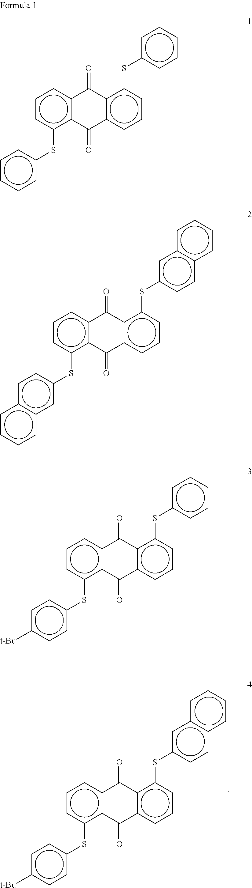

Applications Claiming Priority (2)
| Application Number | Priority Date | Filing Date | Title |
|---|---|---|---|
| KR10-2016-0018272 | 2016-02-17 | ||
| KR1020160018272A KR20170097250A (en) | 2016-02-17 | 2016-02-17 | Display device |
Publications (2)
| Publication Number | Publication Date |
|---|---|
| US20170235191A1 US20170235191A1 (en) | 2017-08-17 |
| US9964806B2 true US9964806B2 (en) | 2018-05-08 |
Family
ID=56851491
Family Applications (1)
| Application Number | Title | Priority Date | Filing Date |
|---|---|---|---|
| US15/229,706 Active 2036-11-12 US9964806B2 (en) | 2016-02-17 | 2016-08-05 | Display device |
Country Status (6)
| Country | Link |
|---|---|
| US (1) | US9964806B2 (en) |
| EP (1) | EP3208655A1 (en) |
| JP (1) | JP2017146580A (en) |
| KR (1) | KR20170097250A (en) |
| CN (1) | CN107092128A (en) |
| TW (1) | TW201732397A (en) |
Cited By (3)
| Publication number | Priority date | Publication date | Assignee | Title |
|---|---|---|---|---|
| US20180067355A1 (en) * | 2015-03-27 | 2018-03-08 | Lg Chem, Ltd. | Reflective liquid crystal device and use thereof |
| US20190049777A1 (en) * | 2017-07-21 | 2019-02-14 | Shenzhen China Star Optoelectronics Technology Co., Ltd. | Display panel and display device |
| US11404458B2 (en) * | 2017-08-14 | 2022-08-02 | Industry-University Cooperation Foundation Hanyang University | Image sensor including quantum dot layer |
Families Citing this family (19)
| Publication number | Priority date | Publication date | Assignee | Title |
|---|---|---|---|---|
| KR20170130648A (en) * | 2016-05-18 | 2017-11-29 | 삼성디스플레이 주식회사 | Display device |
| KR102556273B1 (en) * | 2016-08-23 | 2023-07-17 | 삼성디스플레이 주식회사 | Convexed type display device |
| KR20180072033A (en) | 2016-12-20 | 2018-06-29 | 삼성디스플레이 주식회사 | Display device and manufacturing method thereof |
| US10930710B2 (en) * | 2017-05-04 | 2021-02-23 | Apple Inc. | Display with nanostructure angle-of-view adjustment structures |
| KR102282060B1 (en) * | 2017-05-23 | 2021-07-27 | 삼성디스플레이 주식회사 | Display device and manufacturing method of the same |
| CN107340662A (en) * | 2017-08-31 | 2017-11-10 | 南京中电熊猫液晶显示科技有限公司 | A kind of transparent display and its manufacture method |
| KR102027186B1 (en) * | 2017-09-11 | 2019-10-01 | 서울대학교산학협력단 | Light-modulated quantum dot color display and method for manufacturing the same |
| KR101965529B1 (en) * | 2018-04-06 | 2019-04-03 | 한양대학교 산학협력단 | Dual image sensor including quantum dot layer |
| KR102183681B1 (en) * | 2018-04-20 | 2020-11-27 | 주식회사 엘지화학 | Preparation Method for Alignable Substrate |
| US10879489B2 (en) * | 2018-05-21 | 2020-12-29 | Korea Advanced Institute Of Science And Technology | Organic device having protective film and method of manufacturing the same |
| CN109143662B (en) * | 2018-09-03 | 2021-06-29 | Tcl华星光电技术有限公司 | Quantum dot color filter substrate and display panel |
| KR20200058665A (en) * | 2018-11-19 | 2020-05-28 | 삼성디스플레이 주식회사 | Display device |
| CN113166645B (en) * | 2018-12-26 | 2023-11-21 | Dic株式会社 | Ink composition, light conversion layer, and color filter |
| CN113196875A (en) * | 2018-12-27 | 2021-07-30 | 夏普株式会社 | Display device and method for manufacturing display device |
| KR102273007B1 (en) * | 2019-11-04 | 2021-07-05 | 주식회사 캐머론 | Light controlling plate and its manufacturing method |
| CN111552121B (en) * | 2020-05-08 | 2021-09-24 | 深圳市华星光电半导体显示技术有限公司 | Alignment film, display panel and preparation method thereof |
| CN113126380B (en) * | 2021-04-29 | 2022-09-23 | 昆山龙腾光电股份有限公司 | Liquid crystal display panel and display device |
| CN114355643A (en) * | 2022-01-13 | 2022-04-15 | 中国民用航空飞行学院 | Low color cast display with controllable brightness and visual angle |
| CN114815414B (en) * | 2022-05-16 | 2023-10-24 | 京东方科技集团股份有限公司 | Display panel, display device and preparation method of display panel |
Citations (7)
| Publication number | Priority date | Publication date | Assignee | Title |
|---|---|---|---|---|
| GB2354336A (en) | 1999-07-13 | 2001-03-21 | Screen Technology Ltd | Liquid crystal displays |
| US20020008841A1 (en) | 1998-09-11 | 2002-01-24 | Katsufumi Ohmuro | Flat display device having a liquid crystal panel |
| US20040125305A1 (en) | 1996-02-14 | 2004-07-01 | Semiconductor Energy Laboratory, Co., Ltd., A Japan Corporation | A liquid crystal electro-optical device and method of driving the same. |
| KR20060113160A (en) | 2005-04-29 | 2006-11-02 | 삼성전자주식회사 | Photo-luminescenct liquid crystal display |
| KR20110077932A (en) | 2009-12-30 | 2011-07-07 | 전북대학교산학협력단 | Liquid crystal display apparatus |
| US20130344577A1 (en) | 2012-06-20 | 2013-12-26 | Sony Corporation | Liquid crystal based sensor devices for detecting toxins, bacteria and their activities |
| KR20150039066A (en) | 2013-09-30 | 2015-04-09 | 엘지디스플레이 주식회사 | Stereoscopic image display device using quantum dot color filter and method of fabricating the quantum dot color filter |
Family Cites Families (16)
| Publication number | Priority date | Publication date | Assignee | Title |
|---|---|---|---|---|
| CN1164041A (en) * | 1995-06-30 | 1997-11-05 | 卡西欧计算机公司 | Color liquid crystal display device |
| JPH0915656A (en) * | 1995-06-30 | 1997-01-17 | Casio Comput Co Ltd | Liquid crystal display element |
| JPH10239702A (en) * | 1997-02-28 | 1998-09-11 | Toshiba Corp | Laminated gh liquid crystal display element |
| JP3378465B2 (en) * | 1997-05-16 | 2003-02-17 | 株式会社東芝 | Light emitting device |
| JP2002182228A (en) * | 2000-12-13 | 2002-06-26 | Seiko Epson Corp | Liquid crystal display device and electronic equipment |
| JP2002327176A (en) * | 2001-03-01 | 2002-11-15 | Toshiba Corp | Guest-host liquid crystal composition and liquid crystal display device |
| CN101276011A (en) * | 2007-03-27 | 2008-10-01 | 奇美电子股份有限公司 | Colorful optical filter and manufacturing method thereof |
| JP2009276496A (en) * | 2008-05-14 | 2009-11-26 | Sony Corp | Liquid crystal display device |
| GB0816557D0 (en) * | 2008-09-10 | 2008-10-15 | Merck Patent Gmbh | Electro-optical switching element and electro-optical display |
| CN103033978B (en) * | 2012-12-14 | 2015-04-29 | 京东方科技集团股份有限公司 | Color film substrate and manufacturing method thereof and display device |
| CN103917000B (en) * | 2013-01-07 | 2017-06-13 | 群康科技(深圳)有限公司 | Patterning color changes film and applies its display device |
| KR101408690B1 (en) * | 2013-01-25 | 2014-06-17 | 동아대학교 산학협력단 | Transparent liquid crystal display device |
| JP6106047B2 (en) * | 2013-08-12 | 2017-03-29 | 富士フイルム株式会社 | Optical film, polarizing plate, and liquid crystal display device |
| CN103592710B (en) * | 2013-11-11 | 2016-08-17 | 京东方科技集团股份有限公司 | Color membrane substrates and preparation method thereof, display floater and display device |
| KR102171599B1 (en) * | 2014-05-27 | 2020-10-30 | 삼성디스플레이 주식회사 | Liquid crystal display device and method of fabricating the same |
| CN105068296B (en) * | 2015-09-14 | 2019-02-19 | 深圳市华星光电技术有限公司 | Liquid crystal display device |
-
2016
- 2016-02-17 KR KR1020160018272A patent/KR20170097250A/en not_active Application Discontinuation
- 2016-08-05 US US15/229,706 patent/US9964806B2/en active Active
- 2016-08-31 EP EP16186460.8A patent/EP3208655A1/en not_active Withdrawn
- 2016-09-09 JP JP2016176266A patent/JP2017146580A/en active Pending
- 2016-11-28 CN CN201611069199.9A patent/CN107092128A/en active Pending
-
2017
- 2017-02-17 TW TW106105395A patent/TW201732397A/en unknown
Patent Citations (7)
| Publication number | Priority date | Publication date | Assignee | Title |
|---|---|---|---|---|
| US20040125305A1 (en) | 1996-02-14 | 2004-07-01 | Semiconductor Energy Laboratory, Co., Ltd., A Japan Corporation | A liquid crystal electro-optical device and method of driving the same. |
| US20020008841A1 (en) | 1998-09-11 | 2002-01-24 | Katsufumi Ohmuro | Flat display device having a liquid crystal panel |
| GB2354336A (en) | 1999-07-13 | 2001-03-21 | Screen Technology Ltd | Liquid crystal displays |
| KR20060113160A (en) | 2005-04-29 | 2006-11-02 | 삼성전자주식회사 | Photo-luminescenct liquid crystal display |
| KR20110077932A (en) | 2009-12-30 | 2011-07-07 | 전북대학교산학협력단 | Liquid crystal display apparatus |
| US20130344577A1 (en) | 2012-06-20 | 2013-12-26 | Sony Corporation | Liquid crystal based sensor devices for detecting toxins, bacteria and their activities |
| KR20150039066A (en) | 2013-09-30 | 2015-04-09 | 엘지디스플레이 주식회사 | Stereoscopic image display device using quantum dot color filter and method of fabricating the quantum dot color filter |
Non-Patent Citations (5)
| Title |
|---|
| European Search Report dated Feb. 24, 2017, issued by the EPO for European patent application No. 16186460.8 filed Aug. 31, 2016. |
| Hiroki Iwanaga, "Development of Highly Soluble Anthraquinone Dichroic Dyes and Their Application to Three-Layer Guest-Host Liquid Crystal Displays", Materials 2009, vol. 2, 1636-1661. |
| Hiroki Iwanaga, et al., "Properties of novel yellow anthraquinone dichroic dyes with naphthylthio groups for guest-host liquid crystal displays", Journal of Molecular Structure 975 (2010), pp. 110-114. |
| Vladimir Chigrinov, et al., "Non Polarizer Guest-Host mode based on Dyes with Negative Dichroism", Jpn. J. Appl. Phys., vol. 42 (2003), pp. 1297-1300. |
| Zhenyue Luo, et al., "Quantum Dots Enhanced Liquid Displays", Journal of Display Technology, vol. 10, No. 12, pp. 987-990, Dec. 2014. |
Cited By (4)
| Publication number | Priority date | Publication date | Assignee | Title |
|---|---|---|---|---|
| US20180067355A1 (en) * | 2015-03-27 | 2018-03-08 | Lg Chem, Ltd. | Reflective liquid crystal device and use thereof |
| US10473995B2 (en) * | 2015-03-27 | 2019-11-12 | Lg Chem, Ltd. | Reflective liquid crystal device and use thereof |
| US20190049777A1 (en) * | 2017-07-21 | 2019-02-14 | Shenzhen China Star Optoelectronics Technology Co., Ltd. | Display panel and display device |
| US11404458B2 (en) * | 2017-08-14 | 2022-08-02 | Industry-University Cooperation Foundation Hanyang University | Image sensor including quantum dot layer |
Also Published As
| Publication number | Publication date |
|---|---|
| TW201732397A (en) | 2017-09-16 |
| JP2017146580A (en) | 2017-08-24 |
| CN107092128A (en) | 2017-08-25 |
| KR20170097250A (en) | 2017-08-28 |
| US20170235191A1 (en) | 2017-08-17 |
| EP3208655A1 (en) | 2017-08-23 |
Similar Documents
| Publication | Publication Date | Title |
|---|---|---|
| US9964806B2 (en) | Display device | |
| US11175536B2 (en) | LC-based optical display system | |
| US6809788B2 (en) | Liquid crystal display element with different ratios of polydomain and monodomain states | |
| US8610845B2 (en) | Display device having color filter and polymer-dispersed liquid crystal (PDLC) layer | |
| US7898639B2 (en) | Polymer dispersed liquid crystal display with light emitted layer on the substrate and method of fabricating the same | |
| JP4471014B2 (en) | Liquid crystal display device, backlight light source and optical film | |
| US20170336675A1 (en) | Display device | |
| US11215884B1 (en) | Display panel and display device | |
| WO2013141051A1 (en) | Display panel and display device | |
| CN206515585U (en) | Reflected displaying device | |
| JPH08227071A (en) | Reflection type liquid crystal display element | |
| JP2003140183A (en) | Reflective liquid crystal display device | |
| KR101356272B1 (en) | Polymer Dispersed Liquid Crystal Display and Manafacturing Method Thereof | |
| US20100253891A1 (en) | Liquid crystal display device | |
| CN1127672C (en) | Reflection liquid crystal display device | |
| JP2006195112A (en) | Liquid crystal element, and dimmer element and liquid crystal display device using the same | |
| US20150253619A1 (en) | Liquid crystal display | |
| KR20190015671A (en) | Liquid crystal display device and method of manufacturing the same | |
| US8976317B2 (en) | Display device | |
| JP2000298266A (en) | Polymer-dispersed liquid crystal display panel and its manufacture | |
| US20230251522A1 (en) | Liquid crystal panel and display device | |
| JP2000029021A (en) | Reflective liquid crystal display device | |
| CN1777837A (en) | Liquid crystal display with offset viewing cone | |
| JPH0996810A (en) | Liquid crystal display element and optically anisotropic element | |
| JP2004184670A (en) | Liquid crystal display element |
Legal Events
| Date | Code | Title | Description |
|---|---|---|---|
| AS | Assignment |
Owner name: SAMSUNG DISPLAY CO., LTD., KOREA, REPUBLIC OF Free format text: ASSIGNMENT OF ASSIGNORS INTEREST;ASSIGNORS:JANG, YUN;ROH, NAM SEOK;PARK, SEUNG BEOM;SIGNING DATES FROM 20160711 TO 20160712;REEL/FRAME:039363/0420 |
|
| STCF | Information on status: patent grant |
Free format text: PATENTED CASE |
|
| FEPP | Fee payment procedure |
Free format text: MAINTENANCE FEE REMINDER MAILED (ORIGINAL EVENT CODE: REM.); ENTITY STATUS OF PATENT OWNER: LARGE ENTITY |
|
| FEPP | Fee payment procedure |
Free format text: SURCHARGE FOR LATE PAYMENT, LARGE ENTITY (ORIGINAL EVENT CODE: M1554); ENTITY STATUS OF PATENT OWNER: LARGE ENTITY |
|
| MAFP | Maintenance fee payment |
Free format text: PAYMENT OF MAINTENANCE FEE, 4TH YEAR, LARGE ENTITY (ORIGINAL EVENT CODE: M1551); ENTITY STATUS OF PATENT OWNER: LARGE ENTITY Year of fee payment: 4 |