US9936581B1 - Mechanical and electrical interconnects between conductive threads in fabrics to PCB, FPC, and rigid-flex circuits - Google Patents
Mechanical and electrical interconnects between conductive threads in fabrics to PCB, FPC, and rigid-flex circuits Download PDFInfo
- Publication number
- US9936581B1 US9936581B1 US15/729,482 US201715729482A US9936581B1 US 9936581 B1 US9936581 B1 US 9936581B1 US 201715729482 A US201715729482 A US 201715729482A US 9936581 B1 US9936581 B1 US 9936581B1
- Authority
- US
- United States
- Prior art keywords
- conductive film
- anisotropic conductive
- electrically
- anisotropic
- circuit board
- Prior art date
- Legal status (The legal status is an assumption and is not a legal conclusion. Google has not performed a legal analysis and makes no representation as to the accuracy of the status listed.)
- Expired - Fee Related
Links
Images


Classifications
-
- H—ELECTRICITY
- H05—ELECTRIC TECHNIQUES NOT OTHERWISE PROVIDED FOR
- H05K—PRINTED CIRCUITS; CASINGS OR CONSTRUCTIONAL DETAILS OF ELECTRIC APPARATUS; MANUFACTURE OF ASSEMBLAGES OF ELECTRICAL COMPONENTS
- H05K1/00—Printed circuits
- H05K1/02—Details
- H05K1/14—Structural association of two or more printed circuits
- H05K1/144—Stacked arrangements of planar printed circuit boards
-
- H—ELECTRICITY
- H05—ELECTRIC TECHNIQUES NOT OTHERWISE PROVIDED FOR
- H05K—PRINTED CIRCUITS; CASINGS OR CONSTRUCTIONAL DETAILS OF ELECTRIC APPARATUS; MANUFACTURE OF ASSEMBLAGES OF ELECTRICAL COMPONENTS
- H05K1/00—Printed circuits
- H05K1/02—Details
- H05K1/0277—Bendability or stretchability details
- H05K1/028—Bending or folding regions of flexible printed circuits
-
- H—ELECTRICITY
- H05—ELECTRIC TECHNIQUES NOT OTHERWISE PROVIDED FOR
- H05K—PRINTED CIRCUITS; CASINGS OR CONSTRUCTIONAL DETAILS OF ELECTRIC APPARATUS; MANUFACTURE OF ASSEMBLAGES OF ELECTRICAL COMPONENTS
- H05K1/00—Printed circuits
- H05K1/02—Details
- H05K1/03—Use of materials for the substrate
- H05K1/038—Textiles
-
- H—ELECTRICITY
- H05—ELECTRIC TECHNIQUES NOT OTHERWISE PROVIDED FOR
- H05K—PRINTED CIRCUITS; CASINGS OR CONSTRUCTIONAL DETAILS OF ELECTRIC APPARATUS; MANUFACTURE OF ASSEMBLAGES OF ELECTRICAL COMPONENTS
- H05K1/00—Printed circuits
- H05K1/02—Details
- H05K1/11—Printed elements for providing electric connections to or between printed circuits
- H05K1/118—Printed elements for providing electric connections to or between printed circuits specially for flexible printed circuits, e.g. using folded portions
-
- H—ELECTRICITY
- H05—ELECTRIC TECHNIQUES NOT OTHERWISE PROVIDED FOR
- H05K—PRINTED CIRCUITS; CASINGS OR CONSTRUCTIONAL DETAILS OF ELECTRIC APPARATUS; MANUFACTURE OF ASSEMBLAGES OF ELECTRICAL COMPONENTS
- H05K3/00—Apparatus or processes for manufacturing printed circuits
- H05K3/10—Apparatus or processes for manufacturing printed circuits in which conductive material is applied to the insulating support in such a manner as to form the desired conductive pattern
- H05K3/103—Apparatus or processes for manufacturing printed circuits in which conductive material is applied to the insulating support in such a manner as to form the desired conductive pattern by bonding or embedding conductive wires or strips
-
- H—ELECTRICITY
- H05—ELECTRIC TECHNIQUES NOT OTHERWISE PROVIDED FOR
- H05K—PRINTED CIRCUITS; CASINGS OR CONSTRUCTIONAL DETAILS OF ELECTRIC APPARATUS; MANUFACTURE OF ASSEMBLAGES OF ELECTRICAL COMPONENTS
- H05K3/00—Apparatus or processes for manufacturing printed circuits
- H05K3/22—Secondary treatment of printed circuits
-
- H—ELECTRICITY
- H05—ELECTRIC TECHNIQUES NOT OTHERWISE PROVIDED FOR
- H05K—PRINTED CIRCUITS; CASINGS OR CONSTRUCTIONAL DETAILS OF ELECTRIC APPARATUS; MANUFACTURE OF ASSEMBLAGES OF ELECTRICAL COMPONENTS
- H05K3/00—Apparatus or processes for manufacturing printed circuits
- H05K3/30—Assembling printed circuits with electric components, e.g. with resistors
- H05K3/32—Assembling printed circuits with electric components, e.g. with resistors electrically connecting electric components or wires to printed circuits
- H05K3/321—Assembling printed circuits with electric components, e.g. with resistors electrically connecting electric components or wires to printed circuits by conductive adhesives
- H05K3/323—Assembling printed circuits with electric components, e.g. with resistors electrically connecting electric components or wires to printed circuits by conductive adhesives by applying an anisotropic conductive adhesive layer over an array of pads
-
- H—ELECTRICITY
- H05—ELECTRIC TECHNIQUES NOT OTHERWISE PROVIDED FOR
- H05K—PRINTED CIRCUITS; CASINGS OR CONSTRUCTIONAL DETAILS OF ELECTRIC APPARATUS; MANUFACTURE OF ASSEMBLAGES OF ELECTRICAL COMPONENTS
- H05K3/00—Apparatus or processes for manufacturing printed circuits
- H05K3/46—Manufacturing multilayer circuits
- H05K3/4611—Manufacturing multilayer circuits by laminating two or more circuit boards
- H05K3/4626—Manufacturing multilayer circuits by laminating two or more circuit boards characterised by the insulating layers or materials
- H05K3/4635—Manufacturing multilayer circuits by laminating two or more circuit boards characterised by the insulating layers or materials laminating flexible circuit boards using additional insulating adhesive materials between the boards
-
- H—ELECTRICITY
- H05—ELECTRIC TECHNIQUES NOT OTHERWISE PROVIDED FOR
- H05K—PRINTED CIRCUITS; CASINGS OR CONSTRUCTIONAL DETAILS OF ELECTRIC APPARATUS; MANUFACTURE OF ASSEMBLAGES OF ELECTRICAL COMPONENTS
- H05K2201/00—Indexing scheme relating to printed circuits covered by H05K1/00
- H05K2201/02—Fillers; Particles; Fibers; Reinforcement materials
- H05K2201/0275—Fibers and reinforcement materials
- H05K2201/0281—Conductive fibers
-
- H—ELECTRICITY
- H05—ELECTRIC TECHNIQUES NOT OTHERWISE PROVIDED FOR
- H05K—PRINTED CIRCUITS; CASINGS OR CONSTRUCTIONAL DETAILS OF ELECTRIC APPARATUS; MANUFACTURE OF ASSEMBLAGES OF ELECTRICAL COMPONENTS
- H05K2201/00—Indexing scheme relating to printed circuits covered by H05K1/00
- H05K2201/10—Details of components or other objects attached to or integrated in a printed circuit board
- H05K2201/10227—Other objects, e.g. metallic pieces
- H05K2201/10287—Metal wires as connectors or conductors
Definitions
- the present invention is generally directed to conductive interconnects. More specifically, the present invention is directed to conductive interconnects between a conductive thread or fiber and a flexible printed circuit board.
- Flexible printed circuit boards provide circuit board structures that are less rigid than earlier generation printed circuit boards, and enable varying degrees of flexing, bending and twisting. Flexible interconnects between conductive wires and flexible printed circuit boards are needed for applications where durability and flexibility are a concern.
- an interconnection is made between the conductive wire and the flexible printed circuit board by first forming a contact pad on a top, outer surface of the flexible printed circuit board and then attaching an end of the conductive wire to the contact pad, typically using solder or conductive adhesive. This forms a rigid interconnect between the contact pad and the conductive wire.
- rigid interconnections are susceptible to breaking when subject to physical stress, especially in those applications more prone to bending, flexing and twisting of the flexible printed circuit board.
- An electrically interconnected assembly is a technology enabler for mechanical and electrical interconnects between conductive threads, such as those within fabrics and textiles, to electrical connection points, such as contact pads on a printed circuit board (PCB), a flexible printed circuit (FPC), and/or rigid-flexible circuit board.
- the electrically interconnected assembly uses an anisotropic conductive coated fabric to make an electrical and mechanical interconnect in fabrics or textiles. All fabrics or textiles can be anisotropic conductive coated and cut into sheet form or supplied in roll form.
- an electrically interconnected assembly comprises an electronic device, a first anisotropic conductive film, one or more electrically conductive threads, a second anisotropic conductive film, and a fabric.
- the electronic device has a first surface and one or more electrical connection points on the first surface.
- the first anisotropic conductive film has a first surface and a second surface opposing the first surface, wherein the first anisotropic conductive film is conductive along a z-axis that is perpendicular to the first surface and the second surface, further wherein the second surface of the first anisotropic film is coupled to the first surface of the electronic device.
- the fabric is coupled to the first surface of the second anisotropic conductive film.
- the one or more electrically conductive threads are physically separated from each other.
- the first anisotropic conductive film and the second anisotropic conducting film are non-conducting along a longitudinal plane perpendicular to the z-axis.
- the first anisotropic conductive film comprises a plurality of electrically conductive particles intermixed within an adhesive.
- each electrical connection point comprises a contact pad or solder bump.
- the electronic device comprises a circuit board.
- the circuit board comprises one of a flexible circuit board, a rigid printed circuit board, or a rigid-flexible printed circuit board.
- each electrically conductive thread is one of a metal wire, a thread with an electrically conductive plating finish, an electrically conductive polymer or an electrically conductive fiber.
- the first anisotropic conductive film and the anisotropic conductive film are compressed along the z-axis and non-compressed along an x-y plane.
- a method of fabricating an electrically interconnected assembly includes attaching a first surface of a first anisotropic conductive film to a first surface of an electronic device, wherein the first surface of the electronic device includes one or more electrical connection points.
- the method also includes attaching at least a first portion of each of one or more electrically conductive threads to a second surface of the first anisotropic conductive film, and a second portion of the first portion of each electrically conductive thread is aligned with a corresponding one of the electrical connection points.
- the attached electronic device, first anisotropic conductive film, and one or more electrically conductive threads form a sub-assembly.
- the method also includes attaching a first surface of a second anisotropic conductive film to a fabric to form a cap structure, and stacking the cap structure onto the sub-assembly such that a second surface of the second anisotropic conductive film is positioned on the first portions of the one or more conductive threads.
- the method also includes applying heat and pressure to the stacked cap structure and sub-assembly to form an electrical interconnection between the second portion of each electrically conductive thread and the corresponding one electrical connection point via the first and second anisotropic conductive films.
- applying pressure comprises compressing the first anisotropic conductive film along a z-axis that is perpendicular to the first surface and the second surface of the first anisotropic conductive film, and compressing the second anisotropic conductive film along the z-axis that is perpendicular to a second surface of the second anisotropic conductive film that opposes the first surface of the second anisotropic conductive film.
- the first anisotropic conductive film and the second anisotropic conductive film become conducting along the z-axis due to the applied pressure along the z-axis.
- the first anisotropic conductive film and the second anisotropic conducting film are non-conducting along a longitudinal plane perpendicular to the z-axis.
- the one or more electrically conductive threads are physically separated from each other.
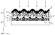
- FIG. 1 illustrates a cut out side view of an electrically interconnected assembly according to some embodiments.
- Embodiments of the present application are directed to a electrically interconnected assembly.
- Those of ordinary skill in the art will realize that the following detailed description of a electrically interconnected assembly is illustrative only and is not intended to be in any way limiting. Other embodiments of a electrically interconnected assembly will readily suggest themselves to such skilled persons having the benefit of this disclosure.
- fabrics and textiles are collectively referred to as fabrics.
- fabric generally applies to cloth or other similar materials made of threads, fibers, filaments or the like. Materials used for fabric threads can include, but are not limited to, cotton, wool, nylon, polyester or other synthetic materials.
- Electrically conductive threads, or simply “conductive threads”, refer to electrically conductive metal wires, threads with an electrically conductive plating finish, electrically conductive polymers or electrically conductive fibers, or the like capable of electrical conductivity.
- An anisotropic conductive layer is made of anisotropic conductive particles mixed within an adhesive material, collectively referred to as an anisotropic conductive film (ACF).
- the conductive particles can be nano-particles or micro-particles made of a conductive material, such as a metal or metal alloy. Examples of such conductive particles include, but are not limited to, nickle-copper particles or gold plated copper particles. The exact material of the conductive particles is application specific.
- the ACF is made into a planar sheet. One planar surface of the ACF sheet is covered with a removable protective carrier, such as a polyethylene terephthalate (PET) carrier or paper. The removable protective carrier can be subsequentlyremoved to expose the planar surface of the ACF.
- PET polyethylene terephthalate
- the removable protective carrier is similar in functionality to the removable backing on two-sided tape.
- a fabric is attached as a protective cover.
- the ACF and the fabric are integrated as a single element.
- the integrated ACF and fabric form a cap structure that provides both mechanical and electrical interconnection for an underlying electrical interconnect.
- the electrical interconnect is formed between a conductive thread and an electrical connection point on a corresponding electronic device. In some embodiments, the electrical interconnect is between a conductive thread and a circuit board having a contact pad to be connected to the conductive thread.
- Multiple electrical interconnects can be formed between multiple conductive threads and multiple electrical connection points, one electrical interconnect for one conductive wire and a corresponding one electrical connection point. Subsequent description is directed to a circuit board and contact pads, but it is understood that such description is generally applicable to other types of electronic devices and corresponding electrical connection points.
- another ACF separate from the cap structure is applied over a surface of a circuit board, including the contact pads, for example copper pads, on the surface of the circuit board.
- the conductive threads are positioned over the other ACF and properly aligned with the corresponding contact pads on the circuit board.
- the cap structure is applied over the conductive threads onto the other ACF to complete the stack-up. Pressure and heat are applied to the stack-up. Each conductive thread becomes electrically connected to its corresponding contact pad via the conductive particles in the other ACF and cap structure.
- the ACF in both the other ACF and the cap structure is anisotropic in that electrical conduction is enabled in the z-axis, the direction of applied pressure, where the z-axis extends perpendicularly between the PET carrier and the fabric, but limited laterally.
- ACF is configured such that in an uncompressed state, the conductive particles are physically separated from each other to prevent electrical conduction from one surface to another. However, upon being compressed in a specific direction, the conductive particles are pressed together in the direction of compression, thereby forming a conductive link parallel to the direction of compression, for example the z-axis, but remaining non-conductive in the direction perpendicular to the direction of compression, for example the x-y plane. When compressed in the z-direction, the conductive particles are pressed together in the z-axis to form columns, each column electrically isolated from adjacent columns due to the original spacing of the particles in the non-compressed ACF. Spacing between adjacent electrically isolated columns can be 100 microns, or smaller.
- the anisotropic nature of the other ACF and cap structure provides electrical interconnectivity between one conductive thread and one corresponding contact pad without short circuiting adjacent conductive threads.
- FIG. 1 illustrates a cut out side view of an electrically interconnected assembly according to some embodiments.
- the electrically interconnected assembly 2 includes a circuit board 4 having one or more contact pads 6 disposed on a surface 32 .
- the circuit board 4 can be any conventional type of circuit board including, but not limited to, a printed circuit board (PCB), a flexible circuit board (FCB), or a rigid-flexible circuit board.
- PCB printed circuit board
- FCB flexible circuit board
- a rigid-flexible circuit board A PCB is more rigid than a FCB or a rigid-flexible circuit board, and can generally be considered as a “rigid” circuit board, although there may be some degree of flexibility.
- the circuit board 4 includes a plurality of stacked layers, the layers made of one or more non-conductive layers and one or more conductive layers.
- the non-conductive layers can be made of rigid material or flexible material.
- Rigid materials can include, but are not limited to, glass-filled material, pre-preg or base material.
- Flexible materials can include, but are not limited to, polyimide, polyethylene teraphthalate (PET), polyethylene nitride (PEN) or polyurethane.
- the conductive layers are each electrically conductive layers made of a metal, such as copper, that is patterned into electrically conductive traces, or interconnects.
- the contact pads 6 provide electrical connection points for corresponding interconnects.
- the circuit board 4 is shown in FIG. 1 as a simple block, but is intended to represent a circuit board of the type described above.
- the electrically interconnected assembly 2 also includes an ACF 8 , conductive threads 12 , an ACF 10 , and a fabric 14 .
- the ACF 8 is adhered to the surface 32 , including contact pads 6 , of the circuit board 4 .
- the fabric 14 is adhered to the ACF 10 .
- the electrically interconnected assembly 2 shown in FIG. 1 shows the completed assembly after heat and pressure have been applied.
- the ACF 8 and ACF 10 are adhered together and compressed in the z-direction with the conductive threads 10 sandwiched in between.
- Each of the ACF 8 and the ACF 10 includes conductive particles 16 distributed throughout an adhesive material 18 .
- Each conductive thread 12 is aligned with a corresponding one of the contact pads 6 .
- an end of the conductive thread 12 is aligned with the corresponding contact pad 6 .
- a portion of the conductive thread 12 other than an end is aligned with the corresponding contact pad 6 .
- the density of the columns is such that at least one or more columns is aligned with each conductive thread 12 and corresponding contact pad 6 .
- the aligned one or more columns provides an electrical interconnect between the conductive thread 12 and corresponding contact pad 6 .
- the conductive particles 16 in the ACF 10 are also compressed together along the z-axis due to the applied compression. Conductive particles 16 aligned in the z-direction with each conductive thread 12 are pushed toward, and with some particles, pushed against the conductive threads 12 in an opposite direction as the conductive particles 16 in the ACF 8 .
- the use of both ACF 8 and ACF 10 acts to envelop, or encase, the perimeter of each conductive thread 12 with conductive particles 16 to create a more robust electrical connection.
- ACF 8 and ACF 10 more securely maintains each conductive thread 12 in position relative to its corresponding contact pad 6 , and also serves as a mechanical stress relief for the connection of the conductive thread 16 to the ACF 8 and underlying contact pad 6 when incorporated onto the fabric 14 .
- FIGS. 2-7 illustrate a method of fabricating an electrically interconnected assembly according to some embodiments.
- the method shown in FIGS. 2-7 is described in relation to the electrically interconnected assembly of FIG. 1 . It is understood that the same methodology can be applied to fabricate similar electrically interconnected assemblies or that similar methodologies can be used to fabricate the same or similar electrically interconnected assembly as that shown in FIG. 1 .
- FIG. 2 illustrates the constituent components of a cap structure prior to assembly.
- the fabric 14 and the ACF 10 are sized to match a footprint of the circuit board 4 or other electrical component to which they are to be applied as a cap structure.
- a footprint of the fabric 14 and a footprint of the ACF 10 are larger than a footprint of the circuit board 4 .
- 0.25 to 0.5 inch portion of oversized fabric and ACF can extend beyond the footprint of the circuit board.
- the portion of the fabric that extends beyond the footprint of the circuit board can be used as attachment area to another substrate, such as another piece of fabric positioned on the opposite side of the circuit board so as to sandwich the circuit board between the two pieces of fabric.
- the footprint of the ACF 10 matches the footprint of the fabric 14 . In other embodiments, the footprint of the ACF 10 is smaller than a footprint of the fabric 14 .
- the ACF 10 is provided as a planar sheet. Planar surface 24 of the ACF 10 is covered with a removable protective carrier 20 , such as a polyethylene terephthalate (PET) carrier or paper.
- the removable protective carrier 20 can be subsequently removed, as shown in FIG. 6 , to expose the planar surface 24 . This exposed planar surface can be subsequently attached to another substrate. In this manner the removable protective carrier 20 is similar in functionality to the removable backing on two-sided tape.
- the fabric 14 is attached to the ACF 10 as a protective cover, as shown in FIG. 3 .
- the ACF 10 and the fabric 14 are integrated as a single element.
- the integrated ACF and fabric form a cap structure 30 .
- the ACF 10 in the cap structure 30 is in a non-compressed state at this step.
- FIG. 4 illustrates the circuit board 4 , the ACF 8 , and the conductive threads 12 prior to assembly.
- the circuit board 4 includes a surface 32 on which contact pads 6 are formed.
- the ACF 8 has opposing surfaces 26 and 28 , surface 26 is covered with a removable protective carrier 21 .
- a footprint of the ACF 8 substantially matches a footprint of the surface 32 of the circuit board 4 .
- the thickness of the ACF 8 may or may not be the same as the thickness of the ACF 10 depending on the application.
- the number of contact pads 6 shown in the figures is for exemplary purposes only and can be more or less than that shown.
- the circuit board 4 is shown as a side-view.
- an array of contact pads can be formed over any portion of the surface 32 in the x-y plane.
- the figures also show the number of conductive threads equaling the number of contact pads. It is understood that only select contact pads may be interconnected to conductive threads, in which case the number of conductive threads is less than the number of contact pads.
- FIG. 5 illustrates the circuit board 4 , the ACF 8 , and the conductive threads 12 assembled in a non-compressed state.
- the surface 28 of the ACF 8 is applied onto the surface 32 and contact pads 6 of the circuit board 4 .
- the carrier 21 is then removed from the surface 26 of the ACF 8 .
- Each conductive thread 12 is then positioned on the surface 26 of the ACF 8 and vertically aligned over a corresponding one of the contact pads 6 .
- the adhesive of the ACF 8 maintains the conductive threads 12 in position during this sub-assembly step.
- an end of the conductive thread is aligned over the corresponding contact pad.
- a portion other than the end of the conductive pad is aligned over the corresponding contact pad.
- each of the conductive threads are shown in the figures as being aligned in parallel. It is understood that this is merely an exemplary alignment pattern and that the conductive threads can be alternatively angled relative to each other, as well as differently from each other, as long as none of the conductive threads overlap each other.
- the assembled circuit board 4 , ACF 8 , and conductive threads 12 form sub-assembly 40 .
- FIG. 6 illustrates the cap structure of FIG. 3 attached to the sub-assembly of FIG. 5 in a non-compressed state.
- the carrier 20 ( FIG. 3 ) from the ACF 10 is removed and the cap structure 30 is positioned onto the sub-assembly 40 with the portions of the conductive threads 12 attached to the ACF 8 sandwiched therebetween.
- the footprints of each of the circuit board 4 , the ACF 8 , the ACF 10 and the fabric 14 are the same. In other embodiments, the size and footprints of the various components can vary relative to each other.
- the footprint of the fabric 14 can be larger than the footprint of the circuit board 4
- the footprint of the ACF 10 can be configured larger than the footprint of the ACF 8 , up to the same size and corresponding footprint of the fabric 14 .
- the portion of the ACF 10 that extends beyond the footprint of the circuit board 4 can be used to adhere the fabric 14 to another substrate, such as a second piece of fabric on the opposite side of the circuit board 4 as the fabric 14 .
- the cap structure 14 functions as a patch over the circuit board 4 which can be attached to another substrate with the circuit board 4 sandwiched in between.
- the cap structure 30 can be attached using a hot bar style attachment method and/or a hot roll method to adhere conductive threads to a PCB, FPC, or rigid-flexible circuit board. It is understood that other conventional techniques can be used to appropriately apply heat and compression. Compression in the z-direction compresses both the ACF 8 and the ACF 10 along the z-axis, but leaves the ACF 8 and the ACF 10 non-compressed in the x-y plane.
- Compression in the z-direction forms the electrically conductive interconnect columns of contacting conductive particles in the ACF 8 and the ACF 10 .
- the contacting conductive particles within the ACF 8 form an electrically conductive interconnect between each conductive thread 12 and corresponding contact pad 6 .
- the contacting conductive particles within the ACF 10 enhance the electrical connection with the conductive thread 12 and the ACF 8 .
- the ACF 10 secures the conductive thread 12 in place relative to the ACF 8 and the corresponding contact pad 6 .
- each conductive thread function to span out electrical interconnections beyond a footprint of the circuit board.
- An opposite end, or another portion of, each conductive thread can be coupled to another electronic device including, but not limited to, another circuit board, a sensor, a microphone, a speaker or a battery. Coupling to the other electrical device can be accomplished using a similar electrically interconnected assembly.
- ACF and an ACF coated fabric provides enhanced mechanical and electrical interconnection of the conductive threads to the contact pads.
- the electrically interconnected assembly eliminates soldered joints and reduces mechanical strain when attaching PCB, FPC, or rigid-flex circuits in wearable fabric and textile products.
- this ACF enhanced structure can be used to electrically and mechanically couple a conductive thread to any type of electronic device that has an electrical connection point.
Landscapes
- Engineering & Computer Science (AREA)
- Microelectronics & Electronic Packaging (AREA)
- Manufacturing & Machinery (AREA)
- Textile Engineering (AREA)
- Combinations Of Printed Boards (AREA)
Abstract
Description
Claims (14)
Priority Applications (1)
| Application Number | Priority Date | Filing Date | Title |
|---|---|---|---|
| US15/729,482 US9936581B1 (en) | 2016-10-11 | 2017-10-10 | Mechanical and electrical interconnects between conductive threads in fabrics to PCB, FPC, and rigid-flex circuits |
Applications Claiming Priority (2)
| Application Number | Priority Date | Filing Date | Title |
|---|---|---|---|
| US201662406516P | 2016-10-11 | 2016-10-11 | |
| US15/729,482 US9936581B1 (en) | 2016-10-11 | 2017-10-10 | Mechanical and electrical interconnects between conductive threads in fabrics to PCB, FPC, and rigid-flex circuits |
Publications (1)
| Publication Number | Publication Date |
|---|---|
| US9936581B1 true US9936581B1 (en) | 2018-04-03 |
Family
ID=61725012
Family Applications (1)
| Application Number | Title | Priority Date | Filing Date |
|---|---|---|---|
| US15/729,482 Expired - Fee Related US9936581B1 (en) | 2016-10-11 | 2017-10-10 | Mechanical and electrical interconnects between conductive threads in fabrics to PCB, FPC, and rigid-flex circuits |
Country Status (1)
| Country | Link |
|---|---|
| US (1) | US9936581B1 (en) |
Cited By (7)
| Publication number | Priority date | Publication date | Assignee | Title |
|---|---|---|---|---|
| US10535845B1 (en) | 2017-07-14 | 2020-01-14 | Flex Ltd. | Flexible and stretchable chain battery |
| CN111051979A (en) * | 2018-08-14 | 2020-04-21 | 现代普脈斯有限公司 | Lighting device with foldable circuit wire and LED and method of manufacturing the same |
| US20200221258A1 (en) * | 2018-07-20 | 2020-07-09 | 3Si Security Systems, Inc. | Flexible anti-theft pack for tracking and location |
| US10863619B2 (en) * | 2018-06-01 | 2020-12-08 | Samsung Display Co., Ltd. | Display apparatus and electronic device including the same |
| US10881001B2 (en) | 2017-03-02 | 2020-12-29 | Flex Ltd. | Micro conductive thread interconnect component to make an interconnect between conductive threads in fabrics to PCB, FPC, and rigid-flex circuits |
| GB2593925A (en) * | 2020-04-09 | 2021-10-13 | Kymira Ltd | Electronic unit for a garment |
| US20240006296A1 (en) * | 2022-07-01 | 2024-01-04 | Intel Corporation | Build up material architecture for microelectronic package device |
Citations (2)
| Publication number | Priority date | Publication date | Assignee | Title |
|---|---|---|---|---|
| US20050110406A1 (en) * | 2003-10-24 | 2005-05-26 | Jeong Young-Chul | Interconnector, method for manufacturing a plasma display device using the same, and a plasma display device with the same |
| US20130270528A1 (en) * | 2012-04-16 | 2013-10-17 | Lg Display Co., Ltd. | Organic light emitting display device and reworking method thereof |
-
2017
- 2017-10-10 US US15/729,482 patent/US9936581B1/en not_active Expired - Fee Related
Patent Citations (2)
| Publication number | Priority date | Publication date | Assignee | Title |
|---|---|---|---|---|
| US20050110406A1 (en) * | 2003-10-24 | 2005-05-26 | Jeong Young-Chul | Interconnector, method for manufacturing a plasma display device using the same, and a plasma display device with the same |
| US20130270528A1 (en) * | 2012-04-16 | 2013-10-17 | Lg Display Co., Ltd. | Organic light emitting display device and reworking method thereof |
Cited By (10)
| Publication number | Priority date | Publication date | Assignee | Title |
|---|---|---|---|---|
| US10881001B2 (en) | 2017-03-02 | 2020-12-29 | Flex Ltd. | Micro conductive thread interconnect component to make an interconnect between conductive threads in fabrics to PCB, FPC, and rigid-flex circuits |
| US10535845B1 (en) | 2017-07-14 | 2020-01-14 | Flex Ltd. | Flexible and stretchable chain battery |
| US10863619B2 (en) * | 2018-06-01 | 2020-12-08 | Samsung Display Co., Ltd. | Display apparatus and electronic device including the same |
| US20200221258A1 (en) * | 2018-07-20 | 2020-07-09 | 3Si Security Systems, Inc. | Flexible anti-theft pack for tracking and location |
| US10812940B2 (en) * | 2018-07-20 | 2020-10-20 | 3Si Security Systems, Inc. | Flexible anti-theft pack for tracking and location |
| CN111051979A (en) * | 2018-08-14 | 2020-04-21 | 现代普脈斯有限公司 | Lighting device with foldable circuit wire and LED and method of manufacturing the same |
| GB2593925A (en) * | 2020-04-09 | 2021-10-13 | Kymira Ltd | Electronic unit for a garment |
| WO2021205188A1 (en) * | 2020-04-09 | 2021-10-14 | Kymira Ltd. | Electronic unit for a garment |
| GB2593925B (en) * | 2020-04-09 | 2023-05-17 | Kymira Ltd | Electronic unit for a garment |
| US20240006296A1 (en) * | 2022-07-01 | 2024-01-04 | Intel Corporation | Build up material architecture for microelectronic package device |
Similar Documents
| Publication | Publication Date | Title |
|---|---|---|
| US10881001B2 (en) | Micro conductive thread interconnect component to make an interconnect between conductive threads in fabrics to PCB, FPC, and rigid-flex circuits | |
| US7595452B2 (en) | Circuit board and method for its production | |
| US11641554B2 (en) | Transducer and manufacturing method thereof | |
| US20130160183A1 (en) | Textile arrangement and method for manufacturing | |
| US20100065320A1 (en) | Wiring board and method for manufacturing the same | |
| JP2004095566A (en) | SHIELD FILM, SHIELD FLEXIBLE PRINTED WIRING BOARD AND PROCESS FOR PRODUCING THEM | |
| US20110100683A1 (en) | Electronic textile | |
| JP6502673B2 (en) | Connection structure, wearable device and manufacturing method of connection structure | |
| US20160211473A1 (en) | Electrically interconnecting foil | |
| WO2008047619A1 (en) | Circuit substrate device and circuit substrate module device | |
| JP2009200113A (en) | Shield wiring circuit board | |
| US10985484B1 (en) | Electronic conductive interconnection for bridging across irregular areas in a textile product | |
| KR20190052840A (en) | Method for bonding flexible sensor on fpcb, and fpcb bonded flexible sensor | |
| JP2006528842A (en) | Flexible circuit connection by stitching | |
| JP7250490B2 (en) | transducer | |
| JPH0737433A (en) | Conductive elastic connector and method of manufacturing the same | |
| CN110278701A (en) | Electromagnetic wave shielding film and shielding printed circuit board | |
| JP2850786B2 (en) | Shield substrate and manufacturing method thereof | |
| JP2011211030A (en) | Wiring board and method of manufacturing the same | |
| JP2011077125A (en) | Wiring board, manufacturing method of wiring board, connection structure of wiring board, and connection method of wiring board | |
| JPH01195607A (en) | Conductive adhesive sheet | |
| US20250376793A1 (en) | Functional fiber and panel interconnect for electronic textiles | |
| JP2007103671A (en) | Conductive wiring board using paralleled lines | |
| WO2006082745A1 (en) | Connection component, multilayer substrate | |
| JPH10326665A (en) | Manufacture of connecting terminal sheet for electric part item |
Legal Events
| Date | Code | Title | Description |
|---|---|---|---|
| AS | Assignment |
Owner name: FLEX LTD., SINGAPORE Free format text: ASSIGNMENT OF ASSIGNORS INTEREST;ASSIGNOR:BERGMAN, MARK;REEL/FRAME:043828/0924 Effective date: 20171010 |
|
| FEPP | Fee payment procedure |
Free format text: ENTITY STATUS SET TO UNDISCOUNTED (ORIGINAL EVENT CODE: BIG.) |
|
| STCF | Information on status: patent grant |
Free format text: PATENTED CASE |
|
| FEPP | Fee payment procedure |
Free format text: SURCHARGE FOR LATE PAYMENT, LARGE ENTITY (ORIGINAL EVENT CODE: M1554); ENTITY STATUS OF PATENT OWNER: LARGE ENTITY |
|
| MAFP | Maintenance fee payment |
Free format text: PAYMENT OF MAINTENANCE FEE, 4TH YEAR, LARGE ENTITY (ORIGINAL EVENT CODE: M1551); ENTITY STATUS OF PATENT OWNER: LARGE ENTITY Year of fee payment: 4 |
|
| FEPP | Fee payment procedure |
Free format text: MAINTENANCE FEE REMINDER MAILED (ORIGINAL EVENT CODE: REM.); ENTITY STATUS OF PATENT OWNER: LARGE ENTITY |
|
| LAPS | Lapse for failure to pay maintenance fees |
Free format text: PATENT EXPIRED FOR FAILURE TO PAY MAINTENANCE FEES (ORIGINAL EVENT CODE: EXP.); ENTITY STATUS OF PATENT OWNER: LARGE ENTITY |
|
| STCH | Information on status: patent discontinuation |
Free format text: PATENT EXPIRED DUE TO NONPAYMENT OF MAINTENANCE FEES UNDER 37 CFR 1.362 |