US9919917B2 - Inertial sensor and method of manufacturing the same - Google Patents
Inertial sensor and method of manufacturing the same Download PDFInfo
- Publication number
- US9919917B2 US9919917B2 US14/514,356 US201414514356A US9919917B2 US 9919917 B2 US9919917 B2 US 9919917B2 US 201414514356 A US201414514356 A US 201414514356A US 9919917 B2 US9919917 B2 US 9919917B2
- Authority
- US
- United States
- Prior art keywords
- substrate
- patterning
- mass body
- membrane
- inertial sensor
- Prior art date
- Legal status (The legal status is an assumption and is not a legal conclusion. Google has not performed a legal analysis and makes no representation as to the accuracy of the status listed.)
- Active, expires
Links
- 238000004519 manufacturing process Methods 0.000 title claims abstract description 15
- 238000000059 patterning Methods 0.000 claims abstract description 94
- 239000012528 membrane Substances 0.000 claims abstract description 70
- 239000000853 adhesive Substances 0.000 claims abstract description 45
- 230000001070 adhesive effect Effects 0.000 claims abstract description 45
- 239000012790 adhesive layer Substances 0.000 claims abstract description 38
- 238000005530 etching Methods 0.000 claims abstract description 31
- 239000000758 substrate Substances 0.000 claims description 78
- 238000000034 method Methods 0.000 claims description 22
- 230000035945 sensitivity Effects 0.000 abstract description 12
- 230000008569 process Effects 0.000 description 15
- 238000006073 displacement reaction Methods 0.000 description 10
- 230000001133 acceleration Effects 0.000 description 9
- 238000000708 deep reactive-ion etching Methods 0.000 description 4
- XUIMIQQOPSSXEZ-UHFFFAOYSA-N Silicon Chemical compound [Si] XUIMIQQOPSSXEZ-UHFFFAOYSA-N 0.000 description 3
- 230000008901 benefit Effects 0.000 description 3
- 239000010410 layer Substances 0.000 description 3
- 229910052710 silicon Inorganic materials 0.000 description 3
- 239000010703 silicon Substances 0.000 description 3
- VYPSYNLAJGMNEJ-UHFFFAOYSA-N Silicium dioxide Chemical compound O=[Si]=O VYPSYNLAJGMNEJ-UHFFFAOYSA-N 0.000 description 2
- 238000013016 damping Methods 0.000 description 2
- 230000000694 effects Effects 0.000 description 2
- 239000012212 insulator Substances 0.000 description 2
- 239000000463 material Substances 0.000 description 2
- 230000004048 modification Effects 0.000 description 2
- 238000012986 modification Methods 0.000 description 2
- 229910052814 silicon oxide Inorganic materials 0.000 description 2
- 239000000126 substance Substances 0.000 description 2
- 238000007792 addition Methods 0.000 description 1
- 239000007864 aqueous solution Substances 0.000 description 1
- 238000006243 chemical reaction Methods 0.000 description 1
- 238000001312 dry etching Methods 0.000 description 1
- 150000002500 ions Chemical class 0.000 description 1
- HFGPZNIAWCZYJU-UHFFFAOYSA-N lead zirconate titanate Chemical compound [O-2].[O-2].[O-2].[O-2].[O-2].[Ti+4].[Zr+4].[Pb+2] HFGPZNIAWCZYJU-UHFFFAOYSA-N 0.000 description 1
- 229910052451 lead zirconate titanate Inorganic materials 0.000 description 1
- 238000003754 machining Methods 0.000 description 1
- 230000002265 prevention Effects 0.000 description 1
- 230000002250 progressing effect Effects 0.000 description 1
- 230000004044 response Effects 0.000 description 1
- 238000006467 substitution reaction Methods 0.000 description 1
- 238000001039 wet etching Methods 0.000 description 1
Images


Classifications
-
- B—PERFORMING OPERATIONS; TRANSPORTING
- B81—MICROSTRUCTURAL TECHNOLOGY
- B81C—PROCESSES OR APPARATUS SPECIALLY ADAPTED FOR THE MANUFACTURE OR TREATMENT OF MICROSTRUCTURAL DEVICES OR SYSTEMS
- B81C1/00—Manufacture or treatment of devices or systems in or on a substrate
- B81C1/00015—Manufacture or treatment of devices or systems in or on a substrate for manufacturing microsystems
- B81C1/00134—Manufacture or treatment of devices or systems in or on a substrate for manufacturing microsystems comprising flexible or deformable structures
- B81C1/00158—Diaphragms, membranes
-
- G—PHYSICS
- G01—MEASURING; TESTING
- G01P—MEASURING LINEAR OR ANGULAR SPEED, ACCELERATION, DECELERATION, OR SHOCK; INDICATING PRESENCE, ABSENCE, OR DIRECTION, OF MOVEMENT
- G01P15/00—Measuring acceleration; Measuring deceleration; Measuring shock, i.e. sudden change of acceleration
- G01P15/02—Measuring acceleration; Measuring deceleration; Measuring shock, i.e. sudden change of acceleration by making use of inertia forces using solid seismic masses
- G01P15/08—Measuring acceleration; Measuring deceleration; Measuring shock, i.e. sudden change of acceleration by making use of inertia forces using solid seismic masses with conversion into electric or magnetic values
-
- G—PHYSICS
- G01—MEASURING; TESTING
- G01C—MEASURING DISTANCES, LEVELS OR BEARINGS; SURVEYING; NAVIGATION; GYROSCOPIC INSTRUMENTS; PHOTOGRAMMETRY OR VIDEOGRAMMETRY
- G01C19/00—Gyroscopes; Turn-sensitive devices using vibrating masses; Turn-sensitive devices without moving masses; Measuring angular rate using gyroscopic effects
- G01C19/56—Turn-sensitive devices using vibrating masses, e.g. vibratory angular rate sensors based on Coriolis forces
-
- G—PHYSICS
- G01—MEASURING; TESTING
- G01P—MEASURING LINEAR OR ANGULAR SPEED, ACCELERATION, DECELERATION, OR SHOCK; INDICATING PRESENCE, ABSENCE, OR DIRECTION, OF MOVEMENT
- G01P15/00—Measuring acceleration; Measuring deceleration; Measuring shock, i.e. sudden change of acceleration
- G01P15/02—Measuring acceleration; Measuring deceleration; Measuring shock, i.e. sudden change of acceleration by making use of inertia forces using solid seismic masses
- G01P15/08—Measuring acceleration; Measuring deceleration; Measuring shock, i.e. sudden change of acceleration by making use of inertia forces using solid seismic masses with conversion into electric or magnetic values
- G01P15/0802—Details
-
- G—PHYSICS
- G01—MEASURING; TESTING
- G01P—MEASURING LINEAR OR ANGULAR SPEED, ACCELERATION, DECELERATION, OR SHOCK; INDICATING PRESENCE, ABSENCE, OR DIRECTION, OF MOVEMENT
- G01P15/00—Measuring acceleration; Measuring deceleration; Measuring shock, i.e. sudden change of acceleration
- G01P15/02—Measuring acceleration; Measuring deceleration; Measuring shock, i.e. sudden change of acceleration by making use of inertia forces using solid seismic masses
- G01P15/08—Measuring acceleration; Measuring deceleration; Measuring shock, i.e. sudden change of acceleration by making use of inertia forces using solid seismic masses with conversion into electric or magnetic values
- G01P15/09—Measuring acceleration; Measuring deceleration; Measuring shock, i.e. sudden change of acceleration by making use of inertia forces using solid seismic masses with conversion into electric or magnetic values by piezoelectric pick-up
- G01P15/0922—Measuring acceleration; Measuring deceleration; Measuring shock, i.e. sudden change of acceleration by making use of inertia forces using solid seismic masses with conversion into electric or magnetic values by piezoelectric pick-up of the bending or flexing mode type
-
- G—PHYSICS
- G01—MEASURING; TESTING
- G01P—MEASURING LINEAR OR ANGULAR SPEED, ACCELERATION, DECELERATION, OR SHOCK; INDICATING PRESENCE, ABSENCE, OR DIRECTION, OF MOVEMENT
- G01P15/00—Measuring acceleration; Measuring deceleration; Measuring shock, i.e. sudden change of acceleration
- G01P15/18—Measuring acceleration; Measuring deceleration; Measuring shock, i.e. sudden change of acceleration in two or more dimensions
-
- H—ELECTRICITY
- H10—SEMICONDUCTOR DEVICES; ELECTRIC SOLID-STATE DEVICES NOT OTHERWISE PROVIDED FOR
- H10N—ELECTRIC SOLID-STATE DEVICES NOT OTHERWISE PROVIDED FOR
- H10N99/00—Subject matter not provided for in other groups of this subclass
-
- B—PERFORMING OPERATIONS; TRANSPORTING
- B81—MICROSTRUCTURAL TECHNOLOGY
- B81B—MICROSTRUCTURAL DEVICES OR SYSTEMS, e.g. MICROMECHANICAL DEVICES
- B81B2201/00—Specific applications of microelectromechanical systems
- B81B2201/02—Sensors
- B81B2201/0228—Inertial sensors
- B81B2201/0235—Accelerometers
-
- B—PERFORMING OPERATIONS; TRANSPORTING
- B81—MICROSTRUCTURAL TECHNOLOGY
- B81B—MICROSTRUCTURAL DEVICES OR SYSTEMS, e.g. MICROMECHANICAL DEVICES
- B81B2203/00—Basic microelectromechanical structures
- B81B2203/05—Type of movement
- B81B2203/053—Translation according to an axis perpendicular to the substrate
-
- B—PERFORMING OPERATIONS; TRANSPORTING
- B81—MICROSTRUCTURAL TECHNOLOGY
- B81B—MICROSTRUCTURAL DEVICES OR SYSTEMS, e.g. MICROMECHANICAL DEVICES
- B81B3/00—Devices comprising flexible or deformable elements, e.g. comprising elastic tongues or membranes
- B81B3/0062—Devices moving in two or more dimensions, i.e. having special features which allow movement in more than one dimension
-
- B—PERFORMING OPERATIONS; TRANSPORTING
- B81—MICROSTRUCTURAL TECHNOLOGY
- B81B—MICROSTRUCTURAL DEVICES OR SYSTEMS, e.g. MICROMECHANICAL DEVICES
- B81B3/00—Devices comprising flexible or deformable elements, e.g. comprising elastic tongues or membranes
- B81B3/0064—Constitution or structural means for improving or controlling the physical properties of a device
- B81B3/0067—Mechanical properties
- B81B3/007—For controlling stiffness, e.g. ribs
-
- B—PERFORMING OPERATIONS; TRANSPORTING
- B81—MICROSTRUCTURAL TECHNOLOGY
- B81C—PROCESSES OR APPARATUS SPECIALLY ADAPTED FOR THE MANUFACTURE OR TREATMENT OF MICROSTRUCTURAL DEVICES OR SYSTEMS
- B81C1/00—Manufacture or treatment of devices or systems in or on a substrate
- B81C1/00436—Shaping materials, i.e. techniques for structuring the substrate or the layers on the substrate
- B81C1/00444—Surface micromachining, i.e. structuring layers on the substrate
- B81C1/00468—Releasing structures
- B81C1/00484—Processes for releasing structures not provided for in group B81C1/00476
-
- B—PERFORMING OPERATIONS; TRANSPORTING
- B81—MICROSTRUCTURAL TECHNOLOGY
- B81C—PROCESSES OR APPARATUS SPECIALLY ADAPTED FOR THE MANUFACTURE OR TREATMENT OF MICROSTRUCTURAL DEVICES OR SYSTEMS
- B81C1/00—Manufacture or treatment of devices or systems in or on a substrate
- B81C1/00436—Shaping materials, i.e. techniques for structuring the substrate or the layers on the substrate
- B81C1/00523—Etching material
- B81C1/00531—Dry etching
-
- B—PERFORMING OPERATIONS; TRANSPORTING
- B81—MICROSTRUCTURAL TECHNOLOGY
- B81C—PROCESSES OR APPARATUS SPECIALLY ADAPTED FOR THE MANUFACTURE OR TREATMENT OF MICROSTRUCTURAL DEVICES OR SYSTEMS
- B81C1/00—Manufacture or treatment of devices or systems in or on a substrate
- B81C1/00436—Shaping materials, i.e. techniques for structuring the substrate or the layers on the substrate
- B81C1/00523—Etching material
- B81C1/00539—Wet etching
-
- B—PERFORMING OPERATIONS; TRANSPORTING
- B81—MICROSTRUCTURAL TECHNOLOGY
- B81C—PROCESSES OR APPARATUS SPECIALLY ADAPTED FOR THE MANUFACTURE OR TREATMENT OF MICROSTRUCTURAL DEVICES OR SYSTEMS
- B81C1/00—Manufacture or treatment of devices or systems in or on a substrate
- B81C1/00436—Shaping materials, i.e. techniques for structuring the substrate or the layers on the substrate
- B81C1/00555—Achieving a desired geometry, i.e. controlling etch rates, anisotropy or selectivity
- B81C1/00563—Avoid or control over-etching
- B81C1/00571—Avoid or control under-cutting
-
- B—PERFORMING OPERATIONS; TRANSPORTING
- B81—MICROSTRUCTURAL TECHNOLOGY
- B81C—PROCESSES OR APPARATUS SPECIALLY ADAPTED FOR THE MANUFACTURE OR TREATMENT OF MICROSTRUCTURAL DEVICES OR SYSTEMS
- B81C2201/00—Manufacture or treatment of microstructural devices or systems
- B81C2201/01—Manufacture or treatment of microstructural devices or systems in or on a substrate
- B81C2201/0101—Shaping material; Structuring the bulk substrate or layers on the substrate; Film patterning
- B81C2201/0128—Processes for removing material
- B81C2201/013—Etching
- B81C2201/0132—Dry etching, i.e. plasma etching, barrel etching, reactive ion etching [RIE], sputter etching or ion milling
-
- B—PERFORMING OPERATIONS; TRANSPORTING
- B81—MICROSTRUCTURAL TECHNOLOGY
- B81C—PROCESSES OR APPARATUS SPECIALLY ADAPTED FOR THE MANUFACTURE OR TREATMENT OF MICROSTRUCTURAL DEVICES OR SYSTEMS
- B81C2201/00—Manufacture or treatment of microstructural devices or systems
- B81C2201/01—Manufacture or treatment of microstructural devices or systems in or on a substrate
- B81C2201/0101—Shaping material; Structuring the bulk substrate or layers on the substrate; Film patterning
- B81C2201/0128—Processes for removing material
- B81C2201/013—Etching
- B81C2201/0133—Wet etching
-
- B—PERFORMING OPERATIONS; TRANSPORTING
- B81—MICROSTRUCTURAL TECHNOLOGY
- B81C—PROCESSES OR APPARATUS SPECIALLY ADAPTED FOR THE MANUFACTURE OR TREATMENT OF MICROSTRUCTURAL DEVICES OR SYSTEMS
- B81C2201/00—Manufacture or treatment of microstructural devices or systems
- B81C2201/01—Manufacture or treatment of microstructural devices or systems in or on a substrate
- B81C2201/0101—Shaping material; Structuring the bulk substrate or layers on the substrate; Film patterning
- B81C2201/0128—Processes for removing material
- B81C2201/013—Etching
- B81C2201/0135—Controlling etch progression
- B81C2201/014—Controlling etch progression by depositing an etch stop layer, e.g. silicon nitride, silicon oxide, metal
-
- C—CHEMISTRY; METALLURGY
- C09—DYES; PAINTS; POLISHES; NATURAL RESINS; ADHESIVES; COMPOSITIONS NOT OTHERWISE PROVIDED FOR; APPLICATIONS OF MATERIALS NOT OTHERWISE PROVIDED FOR
- C09K—MATERIALS FOR MISCELLANEOUS APPLICATIONS, NOT PROVIDED FOR ELSEWHERE
- C09K13/00—Etching, surface-brightening or pickling compositions
- C09K13/04—Etching, surface-brightening or pickling compositions containing an inorganic acid
- C09K13/08—Etching, surface-brightening or pickling compositions containing an inorganic acid containing a fluorine compound
-
- G—PHYSICS
- G01—MEASURING; TESTING
- G01P—MEASURING LINEAR OR ANGULAR SPEED, ACCELERATION, DECELERATION, OR SHOCK; INDICATING PRESENCE, ABSENCE, OR DIRECTION, OF MOVEMENT
- G01P15/00—Measuring acceleration; Measuring deceleration; Measuring shock, i.e. sudden change of acceleration
- G01P15/02—Measuring acceleration; Measuring deceleration; Measuring shock, i.e. sudden change of acceleration by making use of inertia forces using solid seismic masses
- G01P15/08—Measuring acceleration; Measuring deceleration; Measuring shock, i.e. sudden change of acceleration by making use of inertia forces using solid seismic masses with conversion into electric or magnetic values
- G01P2015/0805—Measuring acceleration; Measuring deceleration; Measuring shock, i.e. sudden change of acceleration by making use of inertia forces using solid seismic masses with conversion into electric or magnetic values being provided with a particular type of spring-mass-system for defining the displacement of a seismic mass due to an external acceleration
- G01P2015/0822—Measuring acceleration; Measuring deceleration; Measuring shock, i.e. sudden change of acceleration by making use of inertia forces using solid seismic masses with conversion into electric or magnetic values being provided with a particular type of spring-mass-system for defining the displacement of a seismic mass due to an external acceleration for defining out-of-plane movement of the mass
- G01P2015/084—Measuring acceleration; Measuring deceleration; Measuring shock, i.e. sudden change of acceleration by making use of inertia forces using solid seismic masses with conversion into electric or magnetic values being provided with a particular type of spring-mass-system for defining the displacement of a seismic mass due to an external acceleration for defining out-of-plane movement of the mass the mass being suspended at more than one of its sides, e.g. membrane-type suspension, so as to permit multi-axis movement of the mass
-
- G—PHYSICS
- G01—MEASURING; TESTING
- G01P—MEASURING LINEAR OR ANGULAR SPEED, ACCELERATION, DECELERATION, OR SHOCK; INDICATING PRESENCE, ABSENCE, OR DIRECTION, OF MOVEMENT
- G01P15/00—Measuring acceleration; Measuring deceleration; Measuring shock, i.e. sudden change of acceleration
- G01P15/02—Measuring acceleration; Measuring deceleration; Measuring shock, i.e. sudden change of acceleration by making use of inertia forces using solid seismic masses
- G01P15/08—Measuring acceleration; Measuring deceleration; Measuring shock, i.e. sudden change of acceleration by making use of inertia forces using solid seismic masses with conversion into electric or magnetic values
- G01P2015/0862—Measuring acceleration; Measuring deceleration; Measuring shock, i.e. sudden change of acceleration by making use of inertia forces using solid seismic masses with conversion into electric or magnetic values being provided with particular means being integrated into a MEMS accelerometer structure for providing particular additional functionalities to those of a spring mass system
- G01P2015/0871—Measuring acceleration; Measuring deceleration; Measuring shock, i.e. sudden change of acceleration by making use of inertia forces using solid seismic masses with conversion into electric or magnetic values being provided with particular means being integrated into a MEMS accelerometer structure for providing particular additional functionalities to those of a spring mass system using stopper structures for limiting the travel of the seismic mass
Definitions
- the present invention relates to an inertial sensor and a method of manufacturing the same.
- an inertial sensor has been used in various fields, for example, the military, such as an artificial satellite, a missile, an unmanned aircraft, or the like, vehicles, such as an air bag, electronic stability control (ESC), a black box for a vehicle, or the like, hand shaking prevention of a camcorder, motion sensing of a mobile phone or a game machine, navigation, or the like.
- the military such as an artificial satellite, a missile, an unmanned aircraft, or the like
- vehicles such as an air bag, electronic stability control (ESC), a black box for a vehicle, or the like
- ESC electronic stability control
- camcorder hand shaking prevention of a camcorder
- motion sensing of a mobile phone or a game machine navigation, or the like.
- the inertial sensor generally adopts a configuration in which a mass body is bonded to a flexible substrate such as a membrane, or the like, so as to measure acceleration and angular velocity.
- the inertial sensor may calculate the acceleration by measuring inertial force applied to the mass body and may calculate the angular velocity by measuring Coriolis force applied to the mass body.
- the angular velocity ⁇ may be obtained by sensing the Coriolis force (F) applied to the mass body.
- the mass body when the acceleration a is measured by the inertial sensor, the mass body may be displaced by the inertial force F.
- the angular velocity ⁇ is measured by the inertial sensor, the mass body is vibrated by the motion velocity v.
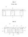
- FIGS. 1 to 3 are process cross-sectional views showing a method of manufacturing an inertial sensor according to the prior art in a process order. A problem of the prior art will be described with reference to FIGS. 1 to 3 .
- a mass body 2 and a post 3 are formed by preparing a silicon on insulator (SOI) substrate and then, selectively removing a support substrate 1 of the SOI substrate.
- SOI silicon on insulator
- an insulating layer 6 (silicon oxide) is selectively removed by supplying an etchant between the mass body 2 and the post 3 , thereby forming an adhesive layer 4 .
- an area of the adhesive layer 4 determines the spring constant of a membrane 5 .
- the area of the adhesive layer 4 is narrow, the area of the membrane 5 having elasticity is substantially wide, such that the spring constant is reduced, thereby increasing the sensitivity of the inertial sensor 10 .
- the area of the adhesive layer 4 is gradually narrow, the area of the adhesive layer 4 is affected by a cross sectional area of the mass body 2 even in the case of considering an undercut phenomenon since the adhesive layer 4 is removed by supplying the etchant between the mass body 2 and the post 3 . Therefore, in order to narrow the area of the adhesive layer 4 , the cross sectional area of the mass body 2 is also narrow. In this case, however, the mass of the mass body 2 is reduced and thus, the sensitivity of the inertial sensor 10 is degraded.
- the inertial sensor 10 has a limitation in improving the sensitivity of the inertial sensor 10 since it is impossible to reduce the spring constant of the membrane 5 while increasing the mass of the mass body 2 in the manufacturing process.
- the present invention has been made in an effort to provide an inertial sensor and a method of manufacturing the same capable of narrowing an area of an adhesive layer by using a mass body including a patterning part patterned to vertically penetrate therethrough so as to reduce a spring constant of a membrane, thereby improving sensitivity of the inertial sensor.
- an inertial sensor including: a plate-shaped membrane; a mass body that includes an adhesive part disposed under a central portion of the membrane and provided at the central portion thereof and a patterning part provided at an outer side of the adhesive part and patterned to vertically penetrate therethrough; and a first adhesive layer that is formed between the membrane and the adhesive part and is provided at an inner side of the patterning part.
- the first adhesive layer may be selectively removed by isotropic etching using the patterning part as a mask to be provided at an inner side of the patterning part.
- the patterning part may be patterned so as to vertically penetrate therethrough by being provided with a plurality of holes.
- the patterning part may be patterned to vertically penetrate therethrough by being provided with a plurality of first rib parts extending to an outer side of the adhesive part from the adhesive part.
- the patterning part may be patterned to vertically penetrate therethrough by being provided with the plurality of first rib parts extending to the outer side of the adhesive part from the adhesive part and a plurality of second rib parts extending to the outer side of the adhesive part from the sides of the first rib parts at each predetermined distance.
- the inertial sensor may further include: a post disposed at a bottom portion of an edge of the membrane so as to surround the mass body; and a second adhesive layer formed between the membrane and the post.
- the inertial sensor may further include a support part that extends from the post in a direction of the mass body and is formed to be spaced apart from the bottom surface of the membrane by a predetermined distance.
- a method of manufacturing an inertial sensor including: (A) preparing a base member in which a first substrate, a second substrate, and a membrane are stacked in order; (B) patterning a patterning part of a mass body including an adhesive part provided at a central portion of the mass body and the patterning part provided at an outer side of the adhesive part so as to vertically penetrate therethrough while patterning the first substrate so as to form the mass body at the central portion of the first substrate; and (C) forming a first adhesive layer on the second substrate remaining at an inner side of the patterning part by selectively removing the second substrate between the membrane and the patterning part by isotropic etching using the patterning part as a mask.
- the patterning part may be patterned so as to vertically penetrate therethrough by being provided with a plurality of holes.
- the patterning part may be patterned so as to vertically penetrate therethrough by forming a plurality of first rib parts extending to an outer side of the adhesive part from the adhesive part.
- the patterning part may be patterned to vertically penetrate therethrough by being provided with the plurality of first rib parts extending to the outer side of the adhesive part from the adhesive part and a plurality of second rib parts extending to the outer side of the adhesive part from the sides of the first rib parts at each predetermined distance.
- the first substrate may be patterned so as to form a post surrounding the mass body at an edge of the first substrate.
- a second adhesive layer may be formed on the second substrate remaining between the membrane and the post by selectively removing the second substrate by isotropic etching using the mass body and the post as a mask.
- the patterning part may be patterned while patterning the first substrate by anisotropic etching.
- the first substrate may be patterned so as to form a support part extending from the post in a direction of the mass body, and at step (C), the support part may be spaced apart from a bottom surface of the membrane by removing the second substrate between the membrane and the support part by isotropic etching.
- FIGS. 1 to 3 are process cross-sectional views showing a method of manufacturing an inertial sensor according to the prior art
- FIG. 4 is a cross-sectional view of an inertial sensor according to a preferred embodiment of the present invention.
- FIG. 5 is a plan view of a mass body and a post of an inertial sensor according to a preferred embodiment of the present invention.
- FIGS. 6 and 7 are plan views showing a modified example of the mass body and the post shown in FIG. 5 ;
- FIG. 8 is a cross-sectional view showing a modified example of the inertial sensor according to the preferred embodiment of the present invention.
- FIG. 9 is a cross-sectional view showing a process of limiting downward displacement of the inertial sensor shown in FIG. 8 ;
- FIG. 10 is a plan view of a mass body, a post, and a support part of the inertial sensor shown in FIG. 8 ;
- FIGS. 11 to 14 are process cross-sectional views showing a method of manufacturing an inertial sensor according to a preferred embodiment of the present invention in a process order.
- FIG. 4 is a cross-sectional view of an inertial sensor according to a preferred embodiment of the present invention
- FIG. 5 is a plan view of a mass body and a post of an inertial sensor according to a preferred embodiment of the present invention
- FIGS. 6 and 7 are plan views showing a modified example of the mass body and the post shown in FIG. 5 .
- an inertial sensor 100 is configured to include a plate-shaped membrane 110 , a mass body 120 that includes an adhesive part 123 disposed under a central portion 113 of the membrane 110 and provided at the central portion thereof and a patterning part 125 provided at an outer side of the adhesive part 123 and patterned to vertically penetrate therethrough, and a first adhesive layer 130 that is formed between the membrane 110 and the adhesive part 123 and is provided at an inner side of the patterning part 125 .
- the membrane 110 is formed in a plate shape and has elasticity so as to vibrate the mass body 120 .
- a boundary of the membrane 110 is not accurately partitioned but may be partitioned into a central portion 113 provided at the center of the membrane 110 and an edge 115 provided along the outside of the membrane 110 .
- the bottom portion of the central portion 113 of the membrane 110 is provided with the mass body 120 , such that the central portion 113 of the membrane 110 is displaced in response to the movement of the mass body 120 .
- the bottom portion of the edge 115 of the membrane 110 is provided with the post 140 to serve to support the central portion 113 of the membrane 110 .
- the membrane 110 is provided with a piezoelectric substance such as lead zirconate titanate and an electrode to sense the displacement of the mass body 120 by using a piezoelectric effect or vibrate the mass body 120 by using an inverse piezoelectric effect.
- the inertial sensor 100 does not necessarily depend on a piezoelectric scheme using the piezoelectric substance, but may depend on all of the driving schemes or the sensing schemes, such as a piezoresistive scheme or a capacitive scheme, which are known to those skilled in the art.
- the mass body 120 is displaced by inertial force or Coriolis force and is disposed at the bottom portion of the central portion 113 of the membrane 110 .
- the mass body 120 is partitioned into the adhesive part 123 provided at the central portion thereof and the patterning part 125 provided at the outer side of the adhesive part 123 .
- the adhesive part 123 is a part that is attached to the bottom surface of the membrane 110 through the first adhesive layer 130 .
- the patterning part 125 is a patterning part so as to vertically penetrate therethrough (a vertical direction with respect to a plate-shaped membrane 110 ) and the first adhesive layer 130 is not present between the patterning part 125 and the bottom surface of the membrane 110 .
- the reason why the first adhesive layer 130 is not present between the patterning part 125 and the membrane 110 is to selectively remove the first adhesive layer 130 by isotropic etching using the patterning part 125 as a mask during a manufacturing process.
- the adhesive part 123 of the mass body 120 is attached to the bottom surface of the membrane 110 by the first adhesive layer 130 and the patterning part 125 is not attached to the bottom surface of the membrane 110 . Therefore, when being compared with the inertial sensor according to the prior art, an area of the first adhesive layer 130 may be narrow and thus, a spring constant of the membrane 110 may be relatively reduced.
- the inertial sensor 100 may reduce the spring constant of the membrane 110 and increase the mass of the mass body 120 , such that the displacement of the mass body 120 may be increased in regards to the same acceleration or angular velocity, thereby making it possible to improve the sensitivity of the inertial sensor 100 .
- the shape of the patterning part 125 of the mass body 120 is not specifically limited if the patterning part 125 is configured to vertically penetrate therethrough so as to be used as the mask.
- the patterning part 125 may be preferably patterned by forming a plurality of holes 126 . More preferably, the plurality of holes 126 may be formed at a predetermined distance ⁇ P (see FIG. 5 ).
- the patterning part 125 may be patterned so as to form rib parts 127 and 128 as shown in FIGS. 6 and 7 .
- the patterning part 125 may be patterned so as to form the plurality of first rib parts 127 that extend to the outer side of the adhesive part 123 from the adhesive part 123 (see FIG. 6 ).
- the patterning part 125 may be patterned so as to form the first rib part 127 and the plurality of second rib parts 128 extending to the outer side of the adhesive part 123 from the side of the first rib part 127 at each predetermined distance (see FIG. 7 ). That is, the patterning part 125 may be patterned so as to form the first rib part 127 or the second rib part 128 by machining a plurality of slits 129 in an outer direction of the adhesive part 123 . Meanwhile, the patterning part 125 is provided with the plurality of machined slits 129 and a support part 160 may be disposed between the slits 129 (see FIG. 10 ). The detailed description thereof will be described below.
- the damping force is reduced due to the viscosity of air at the time of vibration, such that the displacement of the mass body 120 is increased, thereby making it possible to increase the sensitivity of the inertial sensor 100 .
- the first adhesive layer 130 is formed between the membrane 110 and the adhesive part 123 to serve to bond the mass body 120 to the membrane 110 .
- the first adhesive layer 130 is removed by isotropic etching using the patterning part 125 as the mask during the manufacturing process and is thus provided at only the inner side of the patterning part 125 .
- the bottom portion of the edge 115 of the membrane 110 is disposed with the post 140 that supports the membrane 110 .
- the post 140 is formed in a hollow shape surrounding the mass body 120 so as to secure a space that may displace the mass body 120 .
- the post 140 may be formed in a square column shape in which a cavity is formed at the center thereof (see FIG. 5 ).
- a second adhesive layer 150 is formed between the membrane 110 and the post 140 , such that the post 140 is bonded to the bottom surface of the membrane 110 by the second adhesive layer 150 (see FIG. 4 ).
- FIG. 8 is a cross-sectional view showing a modified example of the inertial sensor according to the preferred embodiment of the present invention
- FIG. 9 is a cross-sectional view showing a process of limiting downward displacement of the inertial sensor shown in FIG. 8
- FIG. 10 is a plan view of a mass body, a post, and a support part of the inertial sensor shown in FIG. 8 .
- the inertial sensor 100 may further include the support part 160 that serves to limit the downward displacement of the mass body 120 .
- the support part 160 is not necessarily provided in four and may be formed in two or more along the inner side of the post 140 at equidistance. That is, the support part 160 may be formed in two along the inner side of the post 140 at a distance of 180° or may be formed in three along the inner side of the post 140 at a distance of 120°.
- the pin-shaped support part 160 may extend immediately before the adhesive part 123 of the mass body 120 along between the slits 129 . Therefore, the downward displacement of the mass body 120 may be easily limited and the inner space of the inertial sensor 100 may be efficiently used, by freely controlling the length of the support part 160 while maintaining the size of the mass body 120 .
- the support part 160 is disposed to be spaced apart from the bottom surface of the membrane 110 by a predetermined distance D (see FIG. 8 ).
- the predetermined distance D is a reference limiting the downward displacement of the mass body 120 and even though an excessive force exceeding tolerance is applied to the mass body 120 , the displacement in the downward direction of the mass body 120 is limited to the predetermined distance D between the support part 160 and the membrane 110 (see FIG. 9 ).
- FIGS. 11 to 14 are process cross-sectional views showing a method of manufacturing an inertial sensor according to a preferred embodiment of the present invention in a process order.
- the inertial sensor 100 is configured to include (A) preparing a base member 170 in which a first substrate 180 , a second substrate 190 , and the membrane 110 are stacked in order, (B) patterning the patterning part 125 of the mass body 120 including the adhesive part 123 provided at the central portion of the mass body 120 and the patterning part 125 provided at the outer side of the adhesive part 123 so as to vertically penetrate therethrough while patterning the first substrate 180 so as to form the mass body 120 at the central portion 183 of the first substrate 180 , and (C) forming the first adhesive layer 130 on the second substrate 190 remaining at the inner side of the patterning part 125 by selectively removing the second substrate 190 between the membrane 110 and the patterning part 125 by isotropic etching using the patterning part 125 as the mask.
- a step of preparing the base member 170 in which the first substrate 180 , the second substrate 190 , and the membrane 110 are stacked in order is performed.
- a material of the base member 170 is not specifically limited, but it is preferable to use a silicon on insulator (SOI) substrate to which a micro electro mechanical systems (MEMS) process is easily applied.
- the first substrate 180 is a support substrate of the SOI substrate
- the second substrate 190 is an insulating layer (silicon oxide) of the SOI substrate
- the membrane 110 is an upper silicon layer of the SOI substrate.
- a step of patterning the patterning part 125 of the mass body 120 to vertically penetrate therethrough is performed while forming the mass body 120 by patterning the first substrate 180 .
- the central portion 183 and side portions 185 of the first substrate 180 are provided with the mass body 120 .
- the mass body 120 is partitioned into the adhesive part 123 provided at the central portion of the mass body 120 and the patterning part 125 provided at the outer side of the adhesive part 123 and the patterning part 125 is to vertically penetrate therethrough. Therefore, a mask 187 corresponding to the mass body 120 and the patterning part 125 is disposed on the first substrate 180 (see FIG.
- the etching process may use anisotropic etching so as to remove the first substrate 180 in a vertical direction of the membrane 110 .
- the anisotropic etching is not specifically limited, but may preferably use dry etching and may more preferably use deep reactive ion etching (DRIE).
- the DRIE is a process of performing the etching by simultaneously progressing the physical impact and the chemical reaction of the ions formed by plasma.
- the DRIE may precisely remove the first substrate 180 and may perform the selective etching according to a material, such that only the first substrate 180 among the first substrate 180 and the mask 187 may be etched.
- the plurality of holes 126 may be formed on the patterning part 125 (see FIG. 5 ), the plurality of first rib parts 127 extending to the outer side of the adhesive part 123 from the adhesive part 123 may be formed (see FIG. 6 ), and the plurality of second rib parts 128 extending to the outer side of the adhesive part 123 from the side of the first rib part 127 at each predetermined distance may additionally be formed at the first rib part 127 (see FIG. 7 ).
- the post 140 surrounding the mass body 120 may be formed at the edge of the first substrate 180 while forming the mass body 120 at the central portion 183 of the first substrate 180 by patterning the first substrate 180 .
- the support part 160 extending from the post 140 in the direction of the mass body 120 by patterning the first substrate 180 simultaneously with the mass body 120 and the post 140 may be formed (see FIG. 8 ).
- the mass body 120 , the post 140 , and the support part 160 may be simultaneously formed when the mask 187 corresponding to the shape of the mass body 120 , the post 140 , and the support part 160 is disposed on the first substrate and then, the first substrate 180 is selectively removed by the etching process.
- a step of forming of the first adhesive layer 130 on the second substrate 190 remaining at the inner side of the patterning part 125 by selectively removing the second substrate 190 between the membrane 110 and the patterning part 125 by isotropic etching using the patterning part 125 as the mask is performed.
- the isotropic etching may be performed using the patterning part 125 as the mask at the present step. Since the second substrate 190 is removed by isotropic etching, the undercut phenomenon in which the second substrate 190 is removed in both of the thickness direction and the plane direction occurs.
- the second substrate 190 between the patterning part 125 and the membrane 110 may be removed and the first adhesive layer 130 may finally be formed on the second substrate remaining at only the inner side of the patterning part 125 .
- a predetermined portion R: see an enlarged view of FIG. 14
- the undercut phenomenon occurs at the predetermined portion R from two adjacent holes 126 to remove the second substrate 190 by a predetermined depth ⁇ E in a plane direction.
- the depth ⁇ E in which the second substrate 190 is removed in the plane direction by isotropic etching is larger than 1 ⁇ 2 of the distance ⁇ P of the hole 126 of the patterning part 125 , such that the second substrate 190 between the patterning part 125 and the membrane 110 can be completely removed ( ⁇ E> ⁇ P/2).
- the above contents describe two adjacent holes 126 at the shortest distance ⁇ P as a reference but when the two adjacent holes 126 on a diagonal line are described as the reference, the depth ⁇ E in which the second substrate 190 is removed by isotropic etching to be larger than ⁇ 2 ⁇ 1 ⁇ 2 of the distance ⁇ P between the holes 126 of the patterning part 125 .
- the depth ⁇ E in which the second substrate 190 is removed in the plane direction by isotropic etching is larger than 1 ⁇ 2 of the slit distance ( ⁇ P; see FIGS. 6 to 7 ) of the slit 129 of the patterning part 125 even when the first rib part 127 or the second rib part 128 are formed.
- the isotropic etching is not specifically limited but may use wet etching using an etchant. In this case, as the etchant, an HF aqueous solution may be used.
- the area of the first adhesive layer 130 may be narrow and thus, the spring constant of the membrane 110 is relatively reduced, thereby making it possible to improve the sensitivity of the inertial sensor 100 .
- the second adhesive layer 150 may be formed on the second substrate 190 remaining between the membrane 110 and the post 140 by selectively removing the second substrate 190 by isotropic etching using the mass body 120 and the post 140 as the mask.
- the bottom surface of the membrane 110 may be spaced apart from the support part 160 by removing the second substrate 190 between the membrane 110 and the support part 160 by isotropic etching (see FIG. 8 ).
- the preferred embodiment of the present invention uses the mass body including the patterning part patterned to vertically penetrate therethrough and narrows the area of the adhesive layer by isotropic etching using the patterning part as the mask to reduce the spring constant of the membrane, thereby making it possible to improve the sensitivity of the inertial sensor.
- the preferred embodiment of the present invention freely controls the area of the first adhesive layer by using the patterning part to be designed to widen the cross sectional area of the mass body so as to increase the mass of the mass body, thereby making it possible to improve the sensitivity of the inertial sensor.
- the preferred embodiment of the present invention reduces the damping force due to the viscosity of air at the time of vibration by forming the mass body including a patterning part patterned to vertically penetrate therethrough so as to increase the displacement of the mass body, thereby making it possible to increase the sensitivity of the inertial sensor.
Abstract
Disclosed herein an inertial sensor and a method of manufacturing the same. An inertial sensor 100 according to a preferred embodiment of the present invention is configured to include a plate-shaped membrane 110, a mass body 120 that includes an adhesive part 123 disposed under a central portion 113 of the membrane 110 and provided at the central portion thereof and a patterning part 125 provided at an outer side of the adhesive part 123 and patterned to vertically penetrate therethrough, and a first adhesive layer 130 that is formed between the membrane 110 and the adhesive part 123 and is provided at an inner side of the patterning part 125. An area of the first adhesive layer 130 is narrow by isotropic etching using the patterning part 125 as a mask, thereby making it possible to improve sensitivity of the inertial sensor 100.
Description
This application is a divisional of U.S. patent application Ser. No. 13/177,485 filed on Jul. 6, 2011, which claims the benefit of Korean Patent Application No. 10-2011-0050200, filed on May. 26, 2011, entitled “Inertial Sensor And Method Of Manufacturing The Same” which are hereby incorporated by reference in their entireties into this application.
1. Technical Field
The present invention relates to an inertial sensor and a method of manufacturing the same.
2. Description of the Related Art
Recently, an inertial sensor has been used in various fields, for example, the military, such as an artificial satellite, a missile, an unmanned aircraft, or the like, vehicles, such as an air bag, electronic stability control (ESC), a black box for a vehicle, or the like, hand shaking prevention of a camcorder, motion sensing of a mobile phone or a game machine, navigation, or the like.
The inertial sensor generally adopts a configuration in which a mass body is bonded to a flexible substrate such as a membrane, or the like, so as to measure acceleration and angular velocity. Through the configuration, the inertial sensor may calculate the acceleration by measuring inertial force applied to the mass body and may calculate the angular velocity by measuring Coriolis force applied to the mass body.
A process of measuring the acceleration and the angular velocity by using the inertial sensor will be described in detail below. First, the acceleration may be obtained by Newton's law of motion “F=ma”, where “F” represents inertial force applied to the mass body, “m” represents a mass of the mass body, and “a” is acceleration to be measured. Therefore, the acceleration a may be obtained by sensing the force F applied to the mass body and dividing the sensed force F by the mass m of the mass body that is a predetermined value. Further, the angular velocity may be obtained by Coriolis force “F=2mΩ·v”, where “F” represents the Coriolis force applied to the mass body, “m” represents the mass of the mass body, “Ω” represents the angular velocity to be measured, and “v” represents the motion velocity of the mass body. Among others, since the motion velocity v of the mass body and the mass m of the mass body are values that are known in advance, the angular velocity Ω may be obtained by sensing the Coriolis force (F) applied to the mass body.
As described above, when the acceleration a is measured by the inertial sensor, the mass body may be displaced by the inertial force F. In addition, when the angular velocity Ω is measured by the inertial sensor, the mass body is vibrated by the motion velocity v. As described above, in order to measure the acceleration a or the angular velocity Ω, there is a need to move the mass body according to the elasticity of the membrane and in order to improve the sensitivity of the inertial sensor, it is preferable to make the mass of the mass body large and it is preferable to make a spring constant of the membrane small.
First, as shown in FIGS. 1 and 2 , a mass body 2 and a post 3 are formed by preparing a silicon on insulator (SOI) substrate and then, selectively removing a support substrate 1 of the SOI substrate.
Thereafter, as shown in FIG. 3 , an insulating layer 6 (silicon oxide) is selectively removed by supplying an etchant between the mass body 2 and the post 3, thereby forming an adhesive layer 4. In this case, an area of the adhesive layer 4 determines the spring constant of a membrane 5. In detail, as the area of the adhesive layer 4 is narrow, the area of the membrane 5 having elasticity is substantially wide, such that the spring constant is reduced, thereby increasing the sensitivity of the inertial sensor 10. Therefore, although it is preferable that the area of the adhesive layer 4 is gradually narrow, the area of the adhesive layer 4 is affected by a cross sectional area of the mass body 2 even in the case of considering an undercut phenomenon since the adhesive layer 4 is removed by supplying the etchant between the mass body 2 and the post 3. Therefore, in order to narrow the area of the adhesive layer 4, the cross sectional area of the mass body 2 is also narrow. In this case, however, the mass of the mass body 2 is reduced and thus, the sensitivity of the inertial sensor 10 is degraded.
As a result, the inertial sensor 10 according to the prior art has a limitation in improving the sensitivity of the inertial sensor 10 since it is impossible to reduce the spring constant of the membrane 5 while increasing the mass of the mass body 2 in the manufacturing process.
The present invention has been made in an effort to provide an inertial sensor and a method of manufacturing the same capable of narrowing an area of an adhesive layer by using a mass body including a patterning part patterned to vertically penetrate therethrough so as to reduce a spring constant of a membrane, thereby improving sensitivity of the inertial sensor.
According to a preferred embodiment of the present invention, there is provided an inertial sensor, including: a plate-shaped membrane; a mass body that includes an adhesive part disposed under a central portion of the membrane and provided at the central portion thereof and a patterning part provided at an outer side of the adhesive part and patterned to vertically penetrate therethrough; and a first adhesive layer that is formed between the membrane and the adhesive part and is provided at an inner side of the patterning part.
The first adhesive layer may be selectively removed by isotropic etching using the patterning part as a mask to be provided at an inner side of the patterning part.
The patterning part may be patterned so as to vertically penetrate therethrough by being provided with a plurality of holes.
The patterning part may be patterned to vertically penetrate therethrough by being provided with a plurality of first rib parts extending to an outer side of the adhesive part from the adhesive part.
The patterning part may be patterned to vertically penetrate therethrough by being provided with the plurality of first rib parts extending to the outer side of the adhesive part from the adhesive part and a plurality of second rib parts extending to the outer side of the adhesive part from the sides of the first rib parts at each predetermined distance.
The inertial sensor may further include: a post disposed at a bottom portion of an edge of the membrane so as to surround the mass body; and a second adhesive layer formed between the membrane and the post.
The inertial sensor may further include a support part that extends from the post in a direction of the mass body and is formed to be spaced apart from the bottom surface of the membrane by a predetermined distance.
According to another preferred embodiment of the present invention, there is provided a method of manufacturing an inertial sensor, including: (A) preparing a base member in which a first substrate, a second substrate, and a membrane are stacked in order; (B) patterning a patterning part of a mass body including an adhesive part provided at a central portion of the mass body and the patterning part provided at an outer side of the adhesive part so as to vertically penetrate therethrough while patterning the first substrate so as to form the mass body at the central portion of the first substrate; and (C) forming a first adhesive layer on the second substrate remaining at an inner side of the patterning part by selectively removing the second substrate between the membrane and the patterning part by isotropic etching using the patterning part as a mask.
At step (B), the patterning part may be patterned so as to vertically penetrate therethrough by being provided with a plurality of holes.
At step (B), the patterning part may be patterned so as to vertically penetrate therethrough by forming a plurality of first rib parts extending to an outer side of the adhesive part from the adhesive part.
At step (B), the patterning part may be patterned to vertically penetrate therethrough by being provided with the plurality of first rib parts extending to the outer side of the adhesive part from the adhesive part and a plurality of second rib parts extending to the outer side of the adhesive part from the sides of the first rib parts at each predetermined distance.
At step (B), the first substrate may be patterned so as to form a post surrounding the mass body at an edge of the first substrate.
At step (C), a second adhesive layer may be formed on the second substrate remaining between the membrane and the post by selectively removing the second substrate by isotropic etching using the mass body and the post as a mask.
At step (B), the patterning part may be patterned while patterning the first substrate by anisotropic etching.
At step (B), the first substrate may be patterned so as to form a support part extending from the post in a direction of the mass body, and at step (C), the support part may be spaced apart from a bottom surface of the membrane by removing the second substrate between the membrane and the support part by isotropic etching.
Various features and advantages of the present invention will be more obvious from the following description with reference to the accompanying drawings.
The terms and words used in the present specification and claims should not be interpreted as being limited to typical meanings or dictionary definitions, but should be interpreted as having meanings and concepts relevant to the technical scope of the present invention based on the rule according to which an inventor can appropriately define the concept of the term to describe most appropriately the best method he or she knows for carrying out the invention.
The above and other objects, features and advantages of the present invention will be more clearly understood from the following detailed description taken in conjunction with the accompanying drawings. In the specification, in adding reference numerals to components throughout the drawings, it is to be noted that like reference numerals designate like components even though components are shown in different drawings. Terms used in the specification, ‘first’, ‘second’, etc. can be used to describe various components, but the components are not to be construed as being limited to the terms. The terms are only used to differentiate one component from other components. Further, in describing the present invention, a detailed description of related known functions or configurations will be omitted so as not to obscure the subject of the present invention. Further, when it is determined that the detailed description of the known art related to the present invention may obscure the gist of the present invention, the detailed description will be omitted.
Hereinafter, the preferred embodiments of the present invention will be described in detail with reference to the accompanying drawings.
As shown in FIGS. 4 and 5 , an inertial sensor 100 according to a preferred embodiment of the present invention is configured to include a plate-shaped membrane 110, a mass body 120 that includes an adhesive part 123 disposed under a central portion 113 of the membrane 110 and provided at the central portion thereof and a patterning part 125 provided at an outer side of the adhesive part 123 and patterned to vertically penetrate therethrough, and a first adhesive layer 130 that is formed between the membrane 110 and the adhesive part 123 and is provided at an inner side of the patterning part 125.
The membrane 110 is formed in a plate shape and has elasticity so as to vibrate the mass body 120. In this configuration, a boundary of the membrane 110 is not accurately partitioned but may be partitioned into a central portion 113 provided at the center of the membrane 110 and an edge 115 provided along the outside of the membrane 110. In this case, the bottom portion of the central portion 113 of the membrane 110 is provided with the mass body 120, such that the central portion 113 of the membrane 110 is displaced in response to the movement of the mass body 120. In addition, the bottom portion of the edge 115 of the membrane 110 is provided with the post 140 to serve to support the central portion 113 of the membrane 110. Meanwhile, the membrane 110 is provided with a piezoelectric substance such as lead zirconate titanate and an electrode to sense the displacement of the mass body 120 by using a piezoelectric effect or vibrate the mass body 120 by using an inverse piezoelectric effect. However, the inertial sensor 100 according to the preferred embodiment of the present invention does not necessarily depend on a piezoelectric scheme using the piezoelectric substance, but may depend on all of the driving schemes or the sensing schemes, such as a piezoresistive scheme or a capacitive scheme, which are known to those skilled in the art.
The mass body 120 is displaced by inertial force or Coriolis force and is disposed at the bottom portion of the central portion 113 of the membrane 110. In detail, the mass body 120 is partitioned into the adhesive part 123 provided at the central portion thereof and the patterning part 125 provided at the outer side of the adhesive part 123. In this configuration, the adhesive part 123 is a part that is attached to the bottom surface of the membrane 110 through the first adhesive layer 130. Further, the patterning part 125 is a patterning part so as to vertically penetrate therethrough (a vertical direction with respect to a plate-shaped membrane 110) and the first adhesive layer 130 is not present between the patterning part 125 and the bottom surface of the membrane 110. The reason why the first adhesive layer 130 is not present between the patterning part 125 and the membrane 110 is to selectively remove the first adhesive layer 130 by isotropic etching using the patterning part 125 as a mask during a manufacturing process. As described above, only the adhesive part 123 of the mass body 120 is attached to the bottom surface of the membrane 110 by the first adhesive layer 130 and the patterning part 125 is not attached to the bottom surface of the membrane 110. Therefore, when being compared with the inertial sensor according to the prior art, an area of the first adhesive layer 130 may be narrow and thus, a spring constant of the membrane 110 may be relatively reduced. Further, since an area of the first adhesive layer 130 may be freely controlled by using the patterning part 125, a cross sectional area of the mass body 120 may be widened, thereby making it possible to increase a mass of the mass body 120. As described above, the inertial sensor 100 according to the preferred embodiment of the present invention may reduce the spring constant of the membrane 110 and increase the mass of the mass body 120, such that the displacement of the mass body 120 may be increased in regards to the same acceleration or angular velocity, thereby making it possible to improve the sensitivity of the inertial sensor 100.
Meanwhile, the shape of the patterning part 125 of the mass body 120 is not specifically limited if the patterning part 125 is configured to vertically penetrate therethrough so as to be used as the mask. However, in order to equally remove the first adhesive layer 130 by isotropic etching using the patterning part 125 as the mask, the patterning part 125 may be preferably patterned by forming a plurality of holes 126. More preferably, the plurality of holes 126 may be formed at a predetermined distance ΔP (see FIG. 5 ). In addition to this, the patterning part 125 may be patterned so as to form rib parts 127 and 128 as shown in FIGS. 6 and 7 . In detail, the patterning part 125 may be patterned so as to form the plurality of first rib parts 127 that extend to the outer side of the adhesive part 123 from the adhesive part 123 (see FIG. 6 ). Alternatively, the patterning part 125 may be patterned so as to form the first rib part 127 and the plurality of second rib parts 128 extending to the outer side of the adhesive part 123 from the side of the first rib part 127 at each predetermined distance (see FIG. 7 ). That is, the patterning part 125 may be patterned so as to form the first rib part 127 or the second rib part 128 by machining a plurality of slits 129 in an outer direction of the adhesive part 123. Meanwhile, the patterning part 125 is provided with the plurality of machined slits 129 and a support part 160 may be disposed between the slits 129 (see FIG. 10 ). The detailed description thereof will be described below.
As described above, since the patterning part 125 of the mass body 120 vertically penetrates therethrough to freely communicate with the air, the damping force is reduced due to the viscosity of air at the time of vibration, such that the displacement of the mass body 120 is increased, thereby making it possible to increase the sensitivity of the inertial sensor 100.
As shown in FIG. 4 , the first adhesive layer 130 is formed between the membrane 110 and the adhesive part 123 to serve to bond the mass body 120 to the membrane 110. As described above, the first adhesive layer 130 is removed by isotropic etching using the patterning part 125 as the mask during the manufacturing process and is thus provided at only the inner side of the patterning part 125.
Meanwhile, the bottom portion of the edge 115 of the membrane 110 is disposed with the post 140 that supports the membrane 110. In this configuration, the post 140 is formed in a hollow shape surrounding the mass body 120 so as to secure a space that may displace the mass body 120. For example, the post 140 may be formed in a square column shape in which a cavity is formed at the center thereof (see FIG. 5 ). Meanwhile, a second adhesive layer 150 is formed between the membrane 110 and the post 140, such that the post 140 is bonded to the bottom surface of the membrane 110 by the second adhesive layer 150 (see FIG. 4 ).
As shown in FIGS. 8 to 10 , the inertial sensor 100 according to the preferred embodiment of the present invention may further include the support part 160 that serves to limit the downward displacement of the mass body 120. In this configuration, four support parts 160 are formed in a pin shape along the inner side of the post 140 at a predetermined distance and may extend in the direction of the mass body 120 (see FIG. 10 ). However, the support part 160 is not necessarily provided in four and may be formed in two or more along the inner side of the post 140 at equidistance. That is, the support part 160 may be formed in two along the inner side of the post 140 at a distance of 180° or may be formed in three along the inner side of the post 140 at a distance of 120°. Meanwhile, when the patterning part 125 is provided with the plurality of machined slits 129, the pin-shaped support part 160 may extend immediately before the adhesive part 123 of the mass body 120 along between the slits 129. Therefore, the downward displacement of the mass body 120 may be easily limited and the inner space of the inertial sensor 100 may be efficiently used, by freely controlling the length of the support part 160 while maintaining the size of the mass body 120. In addition, the support part 160 is disposed to be spaced apart from the bottom surface of the membrane 110 by a predetermined distance D (see FIG. 8 ). The predetermined distance D is a reference limiting the downward displacement of the mass body 120 and even though an excessive force exceeding tolerance is applied to the mass body 120, the displacement in the downward direction of the mass body 120 is limited to the predetermined distance D between the support part 160 and the membrane 110 (see FIG. 9 ).
As shown in FIGS. 11 to 14 , the inertial sensor 100 according to the preferred embodiment of the present invention is configured to include (A) preparing a base member 170 in which a first substrate 180, a second substrate 190, and the membrane 110 are stacked in order, (B) patterning the patterning part 125 of the mass body 120 including the adhesive part 123 provided at the central portion of the mass body 120 and the patterning part 125 provided at the outer side of the adhesive part 123 so as to vertically penetrate therethrough while patterning the first substrate 180 so as to form the mass body 120 at the central portion 183 of the first substrate 180, and (C) forming the first adhesive layer 130 on the second substrate 190 remaining at the inner side of the patterning part 125 by selectively removing the second substrate 190 between the membrane 110 and the patterning part 125 by isotropic etching using the patterning part 125 as the mask.
First, as shown in FIG. 11 , a step of preparing the base member 170 in which the first substrate 180, the second substrate 190, and the membrane 110 are stacked in order is performed. In this case, a material of the base member 170 is not specifically limited, but it is preferable to use a silicon on insulator (SOI) substrate to which a micro electro mechanical systems (MEMS) process is easily applied. In this case, the first substrate 180 is a support substrate of the SOI substrate, the second substrate 190 is an insulating layer (silicon oxide) of the SOI substrate, and the membrane 110 is an upper silicon layer of the SOI substrate.
Next, as shown in FIGS. 12 and 13 , a step of patterning the patterning part 125 of the mass body 120 to vertically penetrate therethrough is performed while forming the mass body 120 by patterning the first substrate 180. In detail, the central portion 183 and side portions 185 of the first substrate 180 are provided with the mass body 120. In addition, the mass body 120 is partitioned into the adhesive part 123 provided at the central portion of the mass body 120 and the patterning part 125 provided at the outer side of the adhesive part 123 and the patterning part 125 is to vertically penetrate therethrough. Therefore, a mask 187 corresponding to the mass body 120 and the patterning part 125 is disposed on the first substrate 180 (see FIG. 12 ) and then, the first substrate 180 is selectively removed through an etching process (see FIG. 13 ). In this case, it is preferable that the etching process may use anisotropic etching so as to remove the first substrate 180 in a vertical direction of the membrane 110. The anisotropic etching is not specifically limited, but may preferably use dry etching and may more preferably use deep reactive ion etching (DRIE). The DRIE is a process of performing the etching by simultaneously progressing the physical impact and the chemical reaction of the ions formed by plasma. In particular, the DRIE may precisely remove the first substrate 180 and may perform the selective etching according to a material, such that only the first substrate 180 among the first substrate 180 and the mask 187 may be etched.
In this case, the plurality of holes 126 may be formed on the patterning part 125 (see FIG. 5 ), the plurality of first rib parts 127 extending to the outer side of the adhesive part 123 from the adhesive part 123 may be formed (see FIG. 6 ), and the plurality of second rib parts 128 extending to the outer side of the adhesive part 123 from the side of the first rib part 127 at each predetermined distance may additionally be formed at the first rib part 127 (see FIG. 7 ).
Meanwhile, the post 140 surrounding the mass body 120 may be formed at the edge of the first substrate 180 while forming the mass body 120 at the central portion 183 of the first substrate 180 by patterning the first substrate 180. In addition, the support part 160 extending from the post 140 in the direction of the mass body 120 by patterning the first substrate 180 simultaneously with the mass body 120 and the post 140 may be formed (see FIG. 8 ). In detail, the mass body 120, the post 140, and the support part 160 may be simultaneously formed when the mask 187 corresponding to the shape of the mass body 120, the post 140, and the support part 160 is disposed on the first substrate and then, the first substrate 180 is selectively removed by the etching process.
Next, as shown in FIG. 14 , a step of forming of the first adhesive layer 130 on the second substrate 190 remaining at the inner side of the patterning part 125 by selectively removing the second substrate 190 between the membrane 110 and the patterning part 125 by isotropic etching using the patterning part 125 as the mask is performed. At the previous step, since the patterning part 125 is patterned so as to vertically penetrate therethrough, the isotropic etching may be performed using the patterning part 125 as the mask at the present step. Since the second substrate 190 is removed by isotropic etching, the undercut phenomenon in which the second substrate 190 is removed in both of the thickness direction and the plane direction occurs. Therefore, the second substrate 190 between the patterning part 125 and the membrane 110 may be removed and the first adhesive layer 130 may finally be formed on the second substrate remaining at only the inner side of the patterning part 125. However, in order to completely remove the second substrate 190 between the patterning part 125 and the membrane 110, a predetermined portion (R: see an enlarged view of FIG. 14 ) corresponding between the holes 126 on the second substrate 190 is to be removed. However, the undercut phenomenon occurs at the predetermined portion R from two adjacent holes 126 to remove the second substrate 190 by a predetermined depth ΔE in a plane direction. Therefore, the depth ΔE in which the second substrate 190 is removed in the plane direction by isotropic etching is larger than ½ of the distance ΔP of the hole 126 of the patterning part 125, such that the second substrate 190 between the patterning part 125 and the membrane 110 can be completely removed (ΔE>ΔP/2). However, as shown in an enlarged view of FIG. 5 , the above contents describe two adjacent holes 126 at the shortest distance ΔP as a reference but when the two adjacent holes 126 on a diagonal line are described as the reference, the depth ΔE in which the second substrate 190 is removed by isotropic etching to be larger than √2×½ of the distance ΔP between the holes 126 of the patterning part 125.
In addition, although the case in which the hole 126 is formed on the patterning part 125 is described as the reference, it is preferable that the depth ΔE in which the second substrate 190 is removed in the plane direction by isotropic etching is larger than ½ of the slit distance (ΔP; see FIGS. 6 to 7 ) of the slit 129 of the patterning part 125 even when the first rib part 127 or the second rib part 128 are formed. Meanwhile, the isotropic etching is not specifically limited but may use wet etching using an etchant. In this case, as the etchant, an HF aqueous solution may be used.
As described above, since the first adhesive layer 130 is formed by removing the second substrate 190 between the membrane 110 and the patterning part 125, the area of the first adhesive layer 130 may be narrow and thus, the spring constant of the membrane 110 is relatively reduced, thereby making it possible to improve the sensitivity of the inertial sensor 100.
Meanwhile, at the previous step, when the post 140 is formed by patterning the first substrate 180, at the present step, the second adhesive layer 150 may be formed on the second substrate 190 remaining between the membrane 110 and the post 140 by selectively removing the second substrate 190 by isotropic etching using the mass body 120 and the post 140 as the mask.
Further, at the previous step, when the support part 160 is formed by patterning the first substrate 180, at the present step, the bottom surface of the membrane 110 may be spaced apart from the support part 160 by removing the second substrate 190 between the membrane 110 and the support part 160 by isotropic etching (see FIG. 8 ).
As set forth above, the preferred embodiment of the present invention uses the mass body including the patterning part patterned to vertically penetrate therethrough and narrows the area of the adhesive layer by isotropic etching using the patterning part as the mask to reduce the spring constant of the membrane, thereby making it possible to improve the sensitivity of the inertial sensor.
Further, the preferred embodiment of the present invention freely controls the area of the first adhesive layer by using the patterning part to be designed to widen the cross sectional area of the mass body so as to increase the mass of the mass body, thereby making it possible to improve the sensitivity of the inertial sensor.
In addition, the preferred embodiment of the present invention reduces the damping force due to the viscosity of air at the time of vibration by forming the mass body including a patterning part patterned to vertically penetrate therethrough so as to increase the displacement of the mass body, thereby making it possible to increase the sensitivity of the inertial sensor.
Although the embodiment of the present invention has been disclosed for illustrative purposes, it will be appreciated that an inertial sensor and a method of manufacturing the same according to the invention are not limited thereby, and those skilled in the art will appreciate that various modifications, additions and substitutions are possible, without departing from the scope and spirit of the invention. Accordingly, any and all modifications, variations or equivalent arrangements should be considered to be within the scope of the invention, and the detailed scope of the invention will be disclosed by the accompanying claims.
Claims (7)
1. A method of manufacturing an inertial sensor, comprising:
(A) preparing a base member in which a first substrate, a second substrate, and a membrane are stacked in order;
(B) patterning a patterning part of a mass body including an adhesive part provided at a central portion of the mass body and the patterning part provided at an outer side of the adhesive part so as to vertically penetrate therethrough while patterning the first substrate so as to form the mass body at the central portion of the first substrate; and
(C) forming a first adhesive layer on the second substrate remaining at an inner side of the patterning part by selectively removing the second substrate between the membrane and the patterning part by isotropic etching using the patterning part as a mask,
wherein at step (B), the patterning part is patterned so as to vertically penetrate therethrough by being provided with the plurality of first rib parts extending to the outer side of the adhesive part from the adhesive part and a plurality of second rib parts extending to the outer side of the adhesive part from the sides of the first rib parts at each predetermined distance.
2. The method as set forth in claim 1 , wherein at step (B), the first substrate is patterned so as to form a post surrounding the mass body at an edge of the first substrate.
3. The method as set forth in claim 2 , wherein at step (C), a second adhesive layer is formed on the second substrate remaining between the membrane and the post by selectively removing the second substrate by isotropic etching using the mass body and the post as a mask.
4. The method as set forth in claim 1 , wherein at step (B), the patterning part is patterned while patterning the first substrate by anisotropic etching.
5. The method as set forth in claim 2 , wherein at step (B), the first substrate is patterned so as to form a support part extending from the post in a direction of the mass body, and at step (C), the support part is spaced apart from a bottom surface of the membrane by removing the second substrate between the membrane and the support part by isotropic etching.
6. The method as set forth in claim 1 , wherein at step (B), the patterning part is patterned so as to vertically penetrate therethrough by being provided with a plurality of holes.
7. The method as set forth in claim 1 , wherein at step (B), the patterning part is patterned so as to vertically penetrate therethrough by forming a plurality of first rib parts extending to an outer side of the adhesive part from the adhesive part.
Priority Applications (1)
| Application Number | Priority Date | Filing Date | Title |
|---|---|---|---|
| US14/514,356 US9919917B2 (en) | 2011-05-26 | 2014-10-14 | Inertial sensor and method of manufacturing the same |
Applications Claiming Priority (5)
| Application Number | Priority Date | Filing Date | Title |
|---|---|---|---|
| KR1020110050200 | 2010-05-26 | ||
| KR1020110050200A KR20120131788A (en) | 2011-05-26 | 2011-05-26 | Inertial Sensor And Method of Manufacturing The Same |
| KR10-2011-0050200 | 2011-05-26 | ||
| US13/177,485 US8887569B2 (en) | 2010-05-26 | 2011-07-06 | Inertial sensor and method of manufacturing the same |
| US14/514,356 US9919917B2 (en) | 2011-05-26 | 2014-10-14 | Inertial sensor and method of manufacturing the same |
Related Parent Applications (1)
| Application Number | Title | Priority Date | Filing Date |
|---|---|---|---|
| US13/177,485 Division US8887569B2 (en) | 2010-05-26 | 2011-07-06 | Inertial sensor and method of manufacturing the same |
Publications (2)
| Publication Number | Publication Date |
|---|---|
| US20150031161A1 US20150031161A1 (en) | 2015-01-29 |
| US9919917B2 true US9919917B2 (en) | 2018-03-20 |
Family
ID=45020961
Family Applications (2)
| Application Number | Title | Priority Date | Filing Date |
|---|---|---|---|
| US13/177,485 Active 2032-10-06 US8887569B2 (en) | 2010-05-26 | 2011-07-06 | Inertial sensor and method of manufacturing the same |
| US14/514,356 Active 2033-04-30 US9919917B2 (en) | 2011-05-26 | 2014-10-14 | Inertial sensor and method of manufacturing the same |
Family Applications Before (1)
| Application Number | Title | Priority Date | Filing Date |
|---|---|---|---|
| US13/177,485 Active 2032-10-06 US8887569B2 (en) | 2010-05-26 | 2011-07-06 | Inertial sensor and method of manufacturing the same |
Country Status (2)
| Country | Link |
|---|---|
| US (2) | US8887569B2 (en) |
| KR (1) | KR20120131788A (en) |
Families Citing this family (2)
| Publication number | Priority date | Publication date | Assignee | Title |
|---|---|---|---|---|
| KR101194536B1 (en) * | 2011-04-20 | 2012-10-24 | 삼성전기주식회사 | Method of manufacturing inertial sensor |
| WO2017049278A1 (en) * | 2015-09-18 | 2017-03-23 | Vesper Technologies Inc. | Plate spring |
Citations (8)
| Publication number | Priority date | Publication date | Assignee | Title |
|---|---|---|---|---|
| US5576250A (en) * | 1992-12-28 | 1996-11-19 | Commissariat A L'energie Atomique | Process for the production of accelerometers using silicon on insulator technology |
| US6772632B2 (en) * | 2002-05-13 | 2004-08-10 | Wacoh Corporation | Acceleration sensor and manufacturing method for the same |
| US7357026B2 (en) | 2004-06-03 | 2008-04-15 | Oki Electric Industry Co., Ltd. | Acceleration sensor |
| US7389691B2 (en) * | 2004-12-22 | 2008-06-24 | Oki Electric Industry Co., Ltd. | Acceleration sensor |
| US7845229B2 (en) | 2006-08-11 | 2010-12-07 | Rohm Co., Ltd. | Acceleration sensor |
| US20110215067A1 (en) * | 2006-03-14 | 2011-09-08 | Oki Semiconductor Co., Ltd. | Acceleration sensor with protrusions facing stoppers |
| US20120152020A1 (en) * | 2010-12-15 | 2012-06-21 | Samsung Electro-Mechanics Co., Ltd. | Inertial sensor |
| US20160069926A1 (en) * | 2014-09-04 | 2016-03-10 | Samsung Electro-Mechanics Co., Ltd., | Acceleration sensor and method of manufacturing the same |
-
2011
- 2011-05-26 KR KR1020110050200A patent/KR20120131788A/en not_active Application Discontinuation
- 2011-07-06 US US13/177,485 patent/US8887569B2/en active Active
-
2014
- 2014-10-14 US US14/514,356 patent/US9919917B2/en active Active
Patent Citations (8)
| Publication number | Priority date | Publication date | Assignee | Title |
|---|---|---|---|---|
| US5576250A (en) * | 1992-12-28 | 1996-11-19 | Commissariat A L'energie Atomique | Process for the production of accelerometers using silicon on insulator technology |
| US6772632B2 (en) * | 2002-05-13 | 2004-08-10 | Wacoh Corporation | Acceleration sensor and manufacturing method for the same |
| US7357026B2 (en) | 2004-06-03 | 2008-04-15 | Oki Electric Industry Co., Ltd. | Acceleration sensor |
| US7389691B2 (en) * | 2004-12-22 | 2008-06-24 | Oki Electric Industry Co., Ltd. | Acceleration sensor |
| US20110215067A1 (en) * | 2006-03-14 | 2011-09-08 | Oki Semiconductor Co., Ltd. | Acceleration sensor with protrusions facing stoppers |
| US7845229B2 (en) | 2006-08-11 | 2010-12-07 | Rohm Co., Ltd. | Acceleration sensor |
| US20120152020A1 (en) * | 2010-12-15 | 2012-06-21 | Samsung Electro-Mechanics Co., Ltd. | Inertial sensor |
| US20160069926A1 (en) * | 2014-09-04 | 2016-03-10 | Samsung Electro-Mechanics Co., Ltd., | Acceleration sensor and method of manufacturing the same |
Non-Patent Citations (1)
| Title |
|---|
| Office Action dated Dec. 24, 2013 for U.S. Appl. No. 13/177,485. |
Also Published As
| Publication number | Publication date |
|---|---|
| US20110290022A1 (en) | 2011-12-01 |
| US20150031161A1 (en) | 2015-01-29 |
| US8887569B2 (en) | 2014-11-18 |
| KR20120131788A (en) | 2012-12-05 |
Similar Documents
| Publication | Publication Date | Title |
|---|---|---|
| US8739628B2 (en) | Inertial sensor | |
| US8607638B2 (en) | Micro electro mechanical systems component | |
| CN101553425B (en) | Micro electro mechanical system | |
| US8508105B2 (en) | Inertial sensor | |
| JP6893179B2 (en) | MEMS inertial measuring device with tilted electrodes for orthogonal tuning | |
| JP6067026B2 (en) | Micro electro mechanical system (MEMS) | |
| US8973438B2 (en) | Inertial sensor and method of manufacturing the same | |
| US8701489B2 (en) | Inertial sensor | |
| US9052333B2 (en) | Sensor capable of measuring acceleration, angular velocity, and DC acceleration | |
| US20150241215A1 (en) | Micro electro mechanical systems sensor | |
| US9919917B2 (en) | Inertial sensor and method of manufacturing the same | |
| KR100928761B1 (en) | Capacitance dynamic mass sensor and manufacturing method thereof | |
| KR20120121564A (en) | Inertial Sensor | |
| KR20120105161A (en) | Inertial sensor and method of manufacturing the same | |
| US9052195B2 (en) | Inertial sensor for detecting angular velocity | |
| US20150185010A1 (en) | Acceleration sensor | |
| US8850888B2 (en) | Inertial sensor | |
| CN103723675B (en) | Manufacture method and micromechanical component for micromechanical component | |
| KR101516069B1 (en) | Inertial Sensor | |
| TWI617787B (en) | A microelectromechanical device structure and a method of adjusting a frequency of a mechanical oscillation occuring in a microelectromechanical device structure | |
| US8984942B2 (en) | Suspended masses in micro-mechanical devices | |
| US9212909B2 (en) | Method of manufacturing inertial sensor | |
| US20110296915A1 (en) | Multi-axis capacitive accelerometer | |
| JP2022071262A (en) | Physical quantity sensor, physical quantity sensor device, and inertial measurement device | |
| KR20120133524A (en) | Inertial Sensor |
Legal Events
| Date | Code | Title | Description |
|---|---|---|---|
| AS | Assignment |
Owner name: SAMSUNG ELECTRO-MECHANICS CO., LTD., KOREA, REPUBL Free format text: ASSIGNMENT OF ASSIGNORS INTEREST;ASSIGNORS:KIM, JONG WOON;JEUNG, WON KYU;REEL/FRAME:033962/0923 Effective date: 20110620 |
|
| STCF | Information on status: patent grant |
Free format text: PATENTED CASE |
|
| MAFP | Maintenance fee payment |
Free format text: PAYMENT OF MAINTENANCE FEE, 4TH YEAR, LARGE ENTITY (ORIGINAL EVENT CODE: M1551); ENTITY STATUS OF PATENT OWNER: LARGE ENTITY Year of fee payment: 4 |