US9916999B2 - Methods of fabricating a semiconductor package structure including at least one redistribution layer - Google Patents
Methods of fabricating a semiconductor package structure including at least one redistribution layer Download PDFInfo
- Publication number
- US9916999B2 US9916999B2 US14/731,380 US201514731380A US9916999B2 US 9916999 B2 US9916999 B2 US 9916999B2 US 201514731380 A US201514731380 A US 201514731380A US 9916999 B2 US9916999 B2 US 9916999B2
- Authority
- US
- United States
- Prior art keywords
- layer
- forming
- redistribution
- carrier
- metal
- Prior art date
- Legal status (The legal status is an assumption and is not a legal conclusion. Google has not performed a legal analysis and makes no representation as to the accuracy of the status listed.)
- Active
Links
Images


Classifications
-
- H—ELECTRICITY
- H10—SEMICONDUCTOR DEVICES; ELECTRIC SOLID-STATE DEVICES NOT OTHERWISE PROVIDED FOR
- H10P—GENERIC PROCESSES OR APPARATUS FOR THE MANUFACTURE OR TREATMENT OF DEVICES COVERED BY CLASS H10
- H10P72/00—Handling or holding of wafers, substrates or devices during manufacture or treatment thereof
- H10P72/70—Handling or holding of wafers, substrates or devices during manufacture or treatment thereof for supporting or gripping
- H10P72/74—Handling or holding of wafers, substrates or devices during manufacture or treatment thereof for supporting or gripping using temporarily an auxiliary support
-
- H01L21/6835—
-
- H01L21/4857—
-
- H01L21/6836—
-
- H01L23/5383—
-
- H01L24/92—
-
- H01L24/97—
-
- H—ELECTRICITY
- H10—SEMICONDUCTOR DEVICES; ELECTRIC SOLID-STATE DEVICES NOT OTHERWISE PROVIDED FOR
- H10P—GENERIC PROCESSES OR APPARATUS FOR THE MANUFACTURE OR TREATMENT OF DEVICES COVERED BY CLASS H10
- H10P72/00—Handling or holding of wafers, substrates or devices during manufacture or treatment thereof
- H10P72/70—Handling or holding of wafers, substrates or devices during manufacture or treatment thereof for supporting or gripping
- H10P72/74—Handling or holding of wafers, substrates or devices during manufacture or treatment thereof for supporting or gripping using temporarily an auxiliary support
- H10P72/7402—Wafer tapes, e.g. grinding or dicing support tapes
-
- H—ELECTRICITY
- H10—SEMICONDUCTOR DEVICES; ELECTRIC SOLID-STATE DEVICES NOT OTHERWISE PROVIDED FOR
- H10W—GENERIC PACKAGES, INTERCONNECTIONS, CONNECTORS OR OTHER CONSTRUCTIONAL DETAILS OF DEVICES COVERED BY CLASS H10
- H10W70/00—Package substrates; Interposers; Redistribution layers [RDL]
- H10W70/01—Manufacture or treatment
- H10W70/05—Manufacture or treatment of insulating or insulated package substrates, or of interposers, or of redistribution layers
-
- H—ELECTRICITY
- H10—SEMICONDUCTOR DEVICES; ELECTRIC SOLID-STATE DEVICES NOT OTHERWISE PROVIDED FOR
- H10W—GENERIC PACKAGES, INTERCONNECTIONS, CONNECTORS OR OTHER CONSTRUCTIONAL DETAILS OF DEVICES COVERED BY CLASS H10
- H10W70/00—Package substrates; Interposers; Redistribution layers [RDL]
- H10W70/60—Insulating or insulated package substrates; Interposers; Redistribution layers
- H10W70/611—Insulating or insulated package substrates; Interposers; Redistribution layers for connecting multiple chips together
-
- H—ELECTRICITY
- H10—SEMICONDUCTOR DEVICES; ELECTRIC SOLID-STATE DEVICES NOT OTHERWISE PROVIDED FOR
- H10W—GENERIC PACKAGES, INTERCONNECTIONS, CONNECTORS OR OTHER CONSTRUCTIONAL DETAILS OF DEVICES COVERED BY CLASS H10
- H10W70/00—Package substrates; Interposers; Redistribution layers [RDL]
- H10W70/60—Insulating or insulated package substrates; Interposers; Redistribution layers
- H10W70/67—Insulating or insulated package substrates; Interposers; Redistribution layers characterised by their insulating layers or insulating parts
- H10W70/68—Shapes or dispositions thereof
- H10W70/685—Shapes or dispositions thereof comprising multiple insulating layers
-
- H01L21/78—
-
- H01L2221/68331—
-
- H01L2221/68345—
-
- H01L2221/68359—
-
- H01L2221/68363—
-
- H01L2221/68381—
-
- H01L2224/11—
-
- H01L2224/11312—
-
- H01L2224/1132—
-
- H01L2224/11462—
-
- H01L2224/11464—
-
- H01L2224/131—
-
- H01L2224/13111—
-
- H01L2224/13139—
-
- H01L2224/13144—
-
- H01L2224/13147—
-
- H01L2224/16227—
-
- H01L2224/1703—
-
- H01L2224/17181—
-
- H01L2224/81—
-
- H01L2224/81005—
-
- H01L2224/81192—
-
- H01L2224/92—
-
- H01L2224/97—
-
- H01L23/49816—
-
- H01L23/5385—
-
- H01L24/11—
-
- H01L24/13—
-
- H01L24/16—
-
- H01L24/17—
-
- H01L24/81—
-
- H01L25/0655—
-
- H01L25/18—
-
- H01L25/50—
-
- H01L2924/00014—
-
- H01L2924/014—
-
- H01L2924/15311—
-
- H—ELECTRICITY
- H10—SEMICONDUCTOR DEVICES; ELECTRIC SOLID-STATE DEVICES NOT OTHERWISE PROVIDED FOR
- H10P—GENERIC PROCESSES OR APPARATUS FOR THE MANUFACTURE OR TREATMENT OF DEVICES COVERED BY CLASS H10
- H10P54/00—Cutting or separating of wafers, substrates or parts of devices
-
- H—ELECTRICITY
- H10—SEMICONDUCTOR DEVICES; ELECTRIC SOLID-STATE DEVICES NOT OTHERWISE PROVIDED FOR
- H10P—GENERIC PROCESSES OR APPARATUS FOR THE MANUFACTURE OR TREATMENT OF DEVICES COVERED BY CLASS H10
- H10P72/00—Handling or holding of wafers, substrates or devices during manufacture or treatment thereof
- H10P72/70—Handling or holding of wafers, substrates or devices during manufacture or treatment thereof for supporting or gripping
- H10P72/74—Handling or holding of wafers, substrates or devices during manufacture or treatment thereof for supporting or gripping using temporarily an auxiliary support
- H10P72/7416—Handling or holding of wafers, substrates or devices during manufacture or treatment thereof for supporting or gripping using temporarily an auxiliary support used during dicing or grinding
- H10P72/7418—Handling or holding of wafers, substrates or devices during manufacture or treatment thereof for supporting or gripping using temporarily an auxiliary support used during dicing or grinding of passive members, e.g. a chip mounting substrate
-
- H—ELECTRICITY
- H10—SEMICONDUCTOR DEVICES; ELECTRIC SOLID-STATE DEVICES NOT OTHERWISE PROVIDED FOR
- H10P—GENERIC PROCESSES OR APPARATUS FOR THE MANUFACTURE OR TREATMENT OF DEVICES COVERED BY CLASS H10
- H10P72/00—Handling or holding of wafers, substrates or devices during manufacture or treatment thereof
- H10P72/70—Handling or holding of wafers, substrates or devices during manufacture or treatment thereof for supporting or gripping
- H10P72/74—Handling or holding of wafers, substrates or devices during manufacture or treatment thereof for supporting or gripping using temporarily an auxiliary support
- H10P72/7424—Handling or holding of wafers, substrates or devices during manufacture or treatment thereof for supporting or gripping using temporarily an auxiliary support used as a support during the manufacture of self-supporting substrates
-
- H—ELECTRICITY
- H10—SEMICONDUCTOR DEVICES; ELECTRIC SOLID-STATE DEVICES NOT OTHERWISE PROVIDED FOR
- H10P—GENERIC PROCESSES OR APPARATUS FOR THE MANUFACTURE OR TREATMENT OF DEVICES COVERED BY CLASS H10
- H10P72/00—Handling or holding of wafers, substrates or devices during manufacture or treatment thereof
- H10P72/70—Handling or holding of wafers, substrates or devices during manufacture or treatment thereof for supporting or gripping
- H10P72/74—Handling or holding of wafers, substrates or devices during manufacture or treatment thereof for supporting or gripping using temporarily an auxiliary support
- H10P72/743—Handling or holding of wafers, substrates or devices during manufacture or treatment thereof for supporting or gripping using temporarily an auxiliary support used as a support during manufacture of interconnect decals or build up layers
-
- H—ELECTRICITY
- H10—SEMICONDUCTOR DEVICES; ELECTRIC SOLID-STATE DEVICES NOT OTHERWISE PROVIDED FOR
- H10P—GENERIC PROCESSES OR APPARATUS FOR THE MANUFACTURE OR TREATMENT OF DEVICES COVERED BY CLASS H10
- H10P72/00—Handling or holding of wafers, substrates or devices during manufacture or treatment thereof
- H10P72/70—Handling or holding of wafers, substrates or devices during manufacture or treatment thereof for supporting or gripping
- H10P72/74—Handling or holding of wafers, substrates or devices during manufacture or treatment thereof for supporting or gripping using temporarily an auxiliary support
- H10P72/744—Details of chemical or physical process used for separating the auxiliary support from a device or a wafer
-
- H—ELECTRICITY
- H10—SEMICONDUCTOR DEVICES; ELECTRIC SOLID-STATE DEVICES NOT OTHERWISE PROVIDED FOR
- H10W—GENERIC PACKAGES, INTERCONNECTIONS, CONNECTORS OR OTHER CONSTRUCTIONAL DETAILS OF DEVICES COVERED BY CLASS H10
- H10W72/00—Interconnections or connectors in packages
- H10W72/01—Manufacture or treatment
- H10W72/012—Manufacture or treatment of bump connectors, dummy bumps or thermal bumps
- H10W72/01221—Manufacture or treatment of bump connectors, dummy bumps or thermal bumps using local deposition
- H10W72/01223—Manufacture or treatment of bump connectors, dummy bumps or thermal bumps using local deposition in liquid form, e.g. by dispensing droplets or by screen printing
-
- H—ELECTRICITY
- H10—SEMICONDUCTOR DEVICES; ELECTRIC SOLID-STATE DEVICES NOT OTHERWISE PROVIDED FOR
- H10W—GENERIC PACKAGES, INTERCONNECTIONS, CONNECTORS OR OTHER CONSTRUCTIONAL DETAILS OF DEVICES COVERED BY CLASS H10
- H10W72/00—Interconnections or connectors in packages
- H10W72/01—Manufacture or treatment
- H10W72/012—Manufacture or treatment of bump connectors, dummy bumps or thermal bumps
- H10W72/01231—Manufacture or treatment of bump connectors, dummy bumps or thermal bumps using blanket deposition
- H10W72/01233—Manufacture or treatment of bump connectors, dummy bumps or thermal bumps using blanket deposition in liquid form, e.g. spin coating, spray coating or immersion coating
- H10W72/01235—Manufacture or treatment of bump connectors, dummy bumps or thermal bumps using blanket deposition in liquid form, e.g. spin coating, spray coating or immersion coating by plating, e.g. electroless plating or electroplating
-
- H—ELECTRICITY
- H10—SEMICONDUCTOR DEVICES; ELECTRIC SOLID-STATE DEVICES NOT OTHERWISE PROVIDED FOR
- H10W—GENERIC PACKAGES, INTERCONNECTIONS, CONNECTORS OR OTHER CONSTRUCTIONAL DETAILS OF DEVICES COVERED BY CLASS H10
- H10W72/00—Interconnections or connectors in packages
- H10W72/01—Manufacture or treatment
- H10W72/0198—Manufacture or treatment batch processes
-
- H—ELECTRICITY
- H10—SEMICONDUCTOR DEVICES; ELECTRIC SOLID-STATE DEVICES NOT OTHERWISE PROVIDED FOR
- H10W—GENERIC PACKAGES, INTERCONNECTIONS, CONNECTORS OR OTHER CONSTRUCTIONAL DETAILS OF DEVICES COVERED BY CLASS H10
- H10W72/00—Interconnections or connectors in packages
- H10W72/071—Connecting or disconnecting
- H10W72/072—Connecting or disconnecting of bump connectors
- H10W72/07202—Connecting or disconnecting of bump connectors using auxiliary members
- H10W72/07204—Connecting or disconnecting of bump connectors using auxiliary members using temporary auxiliary members, e.g. sacrificial coatings
- H10W72/07207—Temporary substrates, e.g. removable substrates
-
- H—ELECTRICITY
- H10—SEMICONDUCTOR DEVICES; ELECTRIC SOLID-STATE DEVICES NOT OTHERWISE PROVIDED FOR
- H10W—GENERIC PACKAGES, INTERCONNECTIONS, CONNECTORS OR OTHER CONSTRUCTIONAL DETAILS OF DEVICES COVERED BY CLASS H10
- H10W72/00—Interconnections or connectors in packages
- H10W72/071—Connecting or disconnecting
- H10W72/072—Connecting or disconnecting of bump connectors
- H10W72/07251—Connecting or disconnecting of bump connectors characterised by changes in properties of the bump connectors during connecting
- H10W72/07252—Connecting or disconnecting of bump connectors characterised by changes in properties of the bump connectors during connecting changes in structures or sizes
-
- H—ELECTRICITY
- H10—SEMICONDUCTOR DEVICES; ELECTRIC SOLID-STATE DEVICES NOT OTHERWISE PROVIDED FOR
- H10W—GENERIC PACKAGES, INTERCONNECTIONS, CONNECTORS OR OTHER CONSTRUCTIONAL DETAILS OF DEVICES COVERED BY CLASS H10
- H10W72/00—Interconnections or connectors in packages
- H10W72/071—Connecting or disconnecting
- H10W72/072—Connecting or disconnecting of bump connectors
- H10W72/07251—Connecting or disconnecting of bump connectors characterised by changes in properties of the bump connectors during connecting
- H10W72/07254—Connecting or disconnecting of bump connectors characterised by changes in properties of the bump connectors during connecting changes in dispositions
-
- H—ELECTRICITY
- H10—SEMICONDUCTOR DEVICES; ELECTRIC SOLID-STATE DEVICES NOT OTHERWISE PROVIDED FOR
- H10W—GENERIC PACKAGES, INTERCONNECTIONS, CONNECTORS OR OTHER CONSTRUCTIONAL DETAILS OF DEVICES COVERED BY CLASS H10
- H10W72/00—Interconnections or connectors in packages
- H10W72/20—Bump connectors, e.g. solder bumps or copper pillars; Dummy bumps; Thermal bumps
- H10W72/221—Structures or relative sizes
- H10W72/227—Multiple bumps having different sizes
-
- H—ELECTRICITY
- H10—SEMICONDUCTOR DEVICES; ELECTRIC SOLID-STATE DEVICES NOT OTHERWISE PROVIDED FOR
- H10W—GENERIC PACKAGES, INTERCONNECTIONS, CONNECTORS OR OTHER CONSTRUCTIONAL DETAILS OF DEVICES COVERED BY CLASS H10
- H10W72/00—Interconnections or connectors in packages
- H10W72/20—Bump connectors, e.g. solder bumps or copper pillars; Dummy bumps; Thermal bumps
- H10W72/241—Dispositions, e.g. layouts
- H10W72/247—Dispositions of multiple bumps
-
- H—ELECTRICITY
- H10—SEMICONDUCTOR DEVICES; ELECTRIC SOLID-STATE DEVICES NOT OTHERWISE PROVIDED FOR
- H10W—GENERIC PACKAGES, INTERCONNECTIONS, CONNECTORS OR OTHER CONSTRUCTIONAL DETAILS OF DEVICES COVERED BY CLASS H10
- H10W72/00—Interconnections or connectors in packages
- H10W72/20—Bump connectors, e.g. solder bumps or copper pillars; Dummy bumps; Thermal bumps
- H10W72/251—Materials
- H10W72/252—Materials comprising solid metals or solid metalloids, e.g. PbSn, Ag or Cu
-
- H—ELECTRICITY
- H10—SEMICONDUCTOR DEVICES; ELECTRIC SOLID-STATE DEVICES NOT OTHERWISE PROVIDED FOR
- H10W—GENERIC PACKAGES, INTERCONNECTIONS, CONNECTORS OR OTHER CONSTRUCTIONAL DETAILS OF DEVICES COVERED BY CLASS H10
- H10W90/00—Package configurations
-
- H—ELECTRICITY
- H10—SEMICONDUCTOR DEVICES; ELECTRIC SOLID-STATE DEVICES NOT OTHERWISE PROVIDED FOR
- H10W—GENERIC PACKAGES, INTERCONNECTIONS, CONNECTORS OR OTHER CONSTRUCTIONAL DETAILS OF DEVICES COVERED BY CLASS H10
- H10W90/00—Package configurations
- H10W90/401—Package configurations characterised by multiple insulating or insulated package substrates, interposers or RDLs
-
- H—ELECTRICITY
- H10—SEMICONDUCTOR DEVICES; ELECTRIC SOLID-STATE DEVICES NOT OTHERWISE PROVIDED FOR
- H10W—GENERIC PACKAGES, INTERCONNECTIONS, CONNECTORS OR OTHER CONSTRUCTIONAL DETAILS OF DEVICES COVERED BY CLASS H10
- H10W90/00—Package configurations
- H10W90/701—Package configurations characterised by the relative positions of pads or connectors relative to package parts
- H10W90/721—Package configurations characterised by the relative positions of pads or connectors relative to package parts of bump connectors
- H10W90/724—Package configurations characterised by the relative positions of pads or connectors relative to package parts of bump connectors between a chip and a stacked insulating package substrate, interposer or RDL
-
- H—ELECTRICITY
- H10—SEMICONDUCTOR DEVICES; ELECTRIC SOLID-STATE DEVICES NOT OTHERWISE PROVIDED FOR
- H10W—GENERIC PACKAGES, INTERCONNECTIONS, CONNECTORS OR OTHER CONSTRUCTIONAL DETAILS OF DEVICES COVERED BY CLASS H10
- H10W99/00—Subject matter not provided for in other groups of this subclass
Definitions
- the present disclosure provides a package structure.
- the package structure includes a substrate, a first connector, a redistribution layer, a second connector, and a chip.
- the first connector is disposed over the substrate.
- the redistribution layer is directly disposed over the first connector, and is connected to the substrate by the first connector.
- the redistribution layer includes a block layer, and a metal layer over the block layer.
- the second connector is directly disposed over the redistribution layer, and the chip is connected to the redistribution layer by the second connector.
- the metal layer includes a dielectric layer and a plurality of metal segments.
- the metal segments are disposed in the dielectric layer.
- the first connector interposes the block layer, and connects to the metal layer.
- the block layer is made of silicon carbide, silicon nitride, or a combination thereof.
- the package structure includes a plurality of redistribution layers.
- the metal layers are horizontally aligned, and the different metal layers are connected by a plurality of vias, which penetrate the block layers therebetween.
- the first connector interposes the bottommost layer of the block layers, and connects the bottommost layer of the metal layers and the substrate.
- the first connector and the second connector are independently a solder bump or a solder ball.
- the package structure further includes a passivation layer between the substrate and the redistribution layer, and interposed by the first connector.
- the passivation layer is made of silicon oxide, silicon nitride, benzocyclobutene (BCB), polyimide (PI), polybenzoxazole (PBO), or a combination thereof.
- the present disclosure provides a method for manufacturing a package structure, and the method includes following steps.
- a redistribution layer is formed, including forming a metal layer and forming a block layer over the metal layer.
- a first connector is formed directly on a first side of the redistribution layer.
- a second connector is formed directly on a second side opposite to the first side of the redistribution layer.
- the second side of the redistribution layer is connected to a chip by the second connector.
- the first side of the redistribution layer is connected to a substrate by the first connector.
- the redistribution layer is formed over a first carrier.
- the method further includes connecting the first side of the redistribution layer to a second carrier by the first connector. Then, the first carrier is removed before forming the second connector.
- the method further includes removing the second carrier after bonding the second side of the redistribution layer to the chip.
- the method further includes forming a temporary adhesive over the chip before removing the second carrier. Then, the temporary adhesive is removed after bonding the first side of the redistribution layer to the substrate.
- forming the metal layer is performed by a damascene process.
- forming the metal layer includes depositing a dielectric layer. Next, the dielectric layer is etched to form a plurality of openings. Then, the openings are filled with a metal material to form a plurality of metal segments.
- forming the first connector includes the first connector and interposing the block layer and connecting to the metal layer.
- the method includes forming a plurality of redistribution layers.
- the method further includes forming a passivation layer over the redistribution layer, and interposed by the first connector.
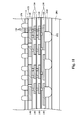
- FIGS. 1A through 1L are cross-sectional views at various stages of fabricating a package structure in accordance with various embodiments of the present disclosure.
- fabricating an interposer including an interposer substrate layer with through-silicon-vias (TSVs) and additional metallization layers built on top of the interposer substrate layer is a complex process.
- TSVs through-silicon-vias
- additional metallization layers built on top of the interposer substrate layer is a complex process.
- the reason is that there are several fabrication steps required to form the interposer substrate layer with the TSVs, which includes forming TSVs within the interposer substrate layer, and performing backside thinning and chemical vapor deposition (CVD) or chemical-mechanical planarization (CMP). These fabrication steps increase the difficulty of wafer-handling.
- CVD chemical vapor deposition
- CMP chemical-mechanical planarization
- the present disclosure provides a package structure and a fabricating method thereof.
- the fabricating method of the present disclosure eliminates the TSV module, and skips the grinding process for the silicon substrate. Therefore, the method provided by the present disclosure has a simpler process flow and a lower process cost.
- FIGS. 1A through 1L are cross-sectional views at various stages of fabricating a package structure 100 ( FIG. 1L ) in accordance with various embodiments of the present disclosure.
- a first passivation layer 112 is formed over a first carrier 202 .
- the first carrier 202 may be made of silicon or glass.
- the first passivation layer 112 is formed by directly depositing over the first carrier 202 .
- the first passivation layer 112 may be formed by directly depositing over the first carrier 202 , or may be formed after forming a release layer.
- the first passivation layer 112 is made of silicon oxide (SiO 2 ), silicon nitride (SiN), benzocyclobutene (BCB), polyimide (PI), polybenzoxazole (PBO), or a combination thereof.
- the redistribution layer includes a metal layer and a block layer, and the metal layer includes a dielectric layer and metal segments disposed in the dielectric layer.
- the metal layer may be formed by a damascene process, such as a single-damascene process and a dual-damascene process.
- the dielectric layer and the metal segments of the metal layer formed by a damascene process are coplanar.
- a metal layer 120 is formed by the process shown in the following FIGS. 1B through 1D .
- FIG. 1B shows that a dielectric layer 122 is deposited over the first passivation layer 112 .
- the dielectric layer 122 is made of silicon oxide (SiO 2 ), silicon nitride (Si 3 N 4 ), or a combination thereof.
- the dielectric layer 122 may be formed by any suitable deposition process. Examples of the deposition include, but are not limited to, chemical vapor deposition (CVD), physical vapor deposition (PVD), atomic layer deposition (ALD), and a combination thereof.
- CVD chemical vapor deposition
- PVD physical vapor deposition
- ALD atomic layer deposition
- the dielectric layer 122 is etched to form a plurality of openings 124 .
- the openings are lines, vias, holes, or trenches.
- the etching may be dry etching or wet etching.
- the openings 124 are filled with a metal material to form a plurality of metal segments 126 .
- the metal segments 126 are formed by deposition.
- the metal segments 126 are made of copper (Cu), aluminum (Al), or a combination thereof.
- a barrier layer may be formed on the sidewalls of the openings 124 before filling the metal material.
- a chemical-mechanical planarization (CMP) process may be performed after filling the openings 124 with the metal material to level the metal segments 126 with the dielectric layer 122 . The metal layer 120 is thereby formed.
- a block layer 130 is formed over the metal layer 120 ( FIG. 1D ).
- the redistribution layer 140 is thereby formed.
- the block layer 130 may be formed by deposition, such as CVD, PVD, ALD, or other suitable process.
- the block layer 130 is made of silicon carbide (SiC), silicon nitride (SiN), or a combination thereof.
- FIGS. 1B through 1E show a process of forming one redistribution layer 140 in accordance with various embodiments of the present disclosure.
- the package structure 100 may include a plurality of redistribution layers 140 depending on the requirement of the product.
- FIG. 1F shows the formed structure with four redistribution layers 140 .
- the block layers 130 between the metal layers 120 are not continuous, and are penetrated by a plurality of vias 128 .
- the vias 128 connect the metal segments 126 of different metal layers 120 .
- the metal layer 120 is formed by a single-damascene process or a dual-damascene process, and portions of the block layers 130 are removed during this process.
- the vias 128 may be formed along with the metal segments 126 .
- a first metal layer including a first dielectric layer and first metal segments is formed.
- a first block layer is formed over the first metal layer.
- a second metal layer is formed by a damascene process, which starts with forming a second dielectric layer over the first block layer. The process continues with removing portions of the second dielectric layer as well as the first block layer to form openings.
- a metal material is filled into the openings to form second metal segments as well as vias penetrating the first block layer.
- a second block layer is formed over the second metal layer. The above steps may be repeated until reaching the required layers of the redistribution layer.
- a second passivation layer 114 is formed over the topmost redistribution layer 140 . Further, portions of the second passivation layer 114 and the topmost block layer 130 are removed to expose portions of the topmost metal layer 120 . Then, a plurality of first connectors 152 is formed directly over the exposed portions of the topmost metal layer 120 . That is, the second passivation layer 114 and the topmost block layer 130 are interposed by the first connectors 152 . Examples of the material of the second passivation layer 114 may refer to counterparts of the first passivation layer 112 , and are not repeated herein. In embodiments, the first connectors 152 are solder bumps or solder balls.
- Material of the first connectors 152 may be silver, copper, or tin-based compositions.
- the first connectors 152 may be formed using electroplating or electroless plating techniques, or using screening or jet printing techniques.
- the first connectors 152 also may be other types of connectors, such as copper or gold pillars, conductive studs, or C4 (controlled collapse chip connection) bumps.
- topmost metal layer 120 or block layer 130 indicated herein represents the relative position of the metal layer 120 or block layer 130 to the first carrier 202 . That is, the “topmost” metal layer 120 or block layer 130 is at the top when the first carrier 202 is at the bottom, and is the farthest metal layer 120 or block layer 130 from the first carrier 202 .
- forming the first connector includes forming an under-bump metallization (UBM) layer over the exposed portion of the topmost metal layer, and forming a first connector body over the UBM layer.
- the UBM layer may be U-shaped, and may cover portions of the second passivation layer 114 .
- Examples of the material of the UBM layer include, but are not limited to, TiN, Ti, Sn, Ag, Cu, Au, Ni, alloys thereof, and a combination thereof.
- the structure shown in FIG. 1G is bonded to a second carrier 204 by the first connectors 152 and an adhesion layer 210 .
- the adhesion layer 210 is formed over the second passivation layer 114 before bonding to the second carrier 204 .
- the first carrier 202 is removed from the first passivation layer 112 .
- the first passivation layer 112 is thereby exposed.
- the first carrier 202 may be made of silicon or glass.
- the first carrier may be removed by grinding and wet etching.
- the first carrier may be removed by laser debonding.
- FIG. 1H shows the structure with the second carrier 204 as the bottommost component.
- the following FIGS. 1H through 1L are inverted relative to FIGS. 1A through 1G .
- portions of the passivation layer 112 are removed to form a plurality of second connectors 154 directly over the topmost metal layer 120 .
- the second connectors 154 are connected to the metal segments 126 of the topmost metal layer 120 .
- Examples of the material of the second connectors 154 may refer to counterparts of the first connectors 152 , and are not repeated herein.
- topmost metal layer 120 indicated herein represents the relative position of the metal layer 120 to the second carrier 204 . That is, the “topmost” metal layer 120 is at the top when the second carrier 204 is at the bottom, and is the farthest metal layer 120 from the second carrier 204 . Further, FIG. 1I is inverted relative to FIG. 1G . Hence, the “topmost metal layer 120 ” referred herein is different from the “topmost metal layer 120 ” discussed above in accordance with FIG. 1G .
- chips 160 are mounted over the second connectors 154 .
- the chips 160 are connected to the redistribution layer 140 by the second connectors 154 .
- the chips 160 are connected to the topmost metal layer 120 by the second connectors 154 .
- the “topmost metal layer 120 ” indicated herein represents the relative position of the metal layer 120 to the second carrier 204 .
- the chips 160 may be the same or different types of chips.
- a temporary adhesive 220 is formed over the chips 160 .
- the temporary adhesive 220 is used to connect the chips 160 , and sustains the structure for the subsequent process of removing the second carrier 204 .
- the temporary adhesive 220 may be a dicing tape.
- the second carrier 204 and the adhesion layer 210 are removed.
- the second carrier 204 may be removed by any suitable methods, such as temporary bonding/debonding (TB/DB) technology. For instance, the second carrier 204 is removed by mechanical debonding or laser debonding.
- a dicing process is performed to the structure shown in FIG. 1K along the dotted lines to separate the chips 160 .
- the diced structure is mounted on a substrate 170 to form the package structure 100 shown in FIG. 1L .
- the substrate 170 is connected to the redistribution layer 140 by the first connectors 152 .
- the substrate 170 is connected to the bottommost layer of the metal layers 120 by the first connectors 152 .
- the package structure 100 is thereby formed.
- the substrate may be a board, such as a printed circuit board (PCB).
- the “bottommost” metal layer 120 indicated herein represents the relative position of the metal layer 120 to the substrate 170 . That is, the “bottommost” metal layer 120 is the nearest metal layer 120 to the substrate 170 when the substrate 170 is at the bottom. Further, FIG. 1L is inverted relative to FIG. 1G . Hence, the “bottommost metal layer 120 ” referred herein is the same as the “topmost metal layer 120 ” discussed above in accordance with FIG. 1G .
- the package structure further includes third connectors 156 under the substrate 170 .
- Examples of material of the third connectors 156 may refer to counterparts of the first connectors 152 , and are not repeated herein.
- the method for fabricating the package structure of the present disclosure is TSV-less and silicon-substrate-less, which means that the method of the present disclosure eliminates the process of forming an interposer substrate layer with TSVs.
- the redistribution layer in the package structure is formed to directly connect to the substrate and the chip.
- the formed package structure includes the block layer adjacent to the metal layer. Therefore, the method for fabricating the package structure of the present disclosure includes a simpler process flow by eliminating the TSV module and skipping silicon grinding process, and thereby having a lower process cost.
- the package structure 100 fabricated by the process shown in FIGS. 1A through 1L includes a substrate 170 , first connector 152 , second connectors 154 , third connectors 156 , redistribution layers 140 , a first passivation layer 112 , a second passivation layer 114 , and chips 160 .
- the substrate 170 is disposed over the third connectors 156 .
- the first connectors 154 are disposed over the substrate 170 .
- the second passivation layer 114 is disposed under the bottommost redistribution layer 140 , and is interposed by the first connectors 152 .
- the redistribution layers 140 are directly disposed over the first connectors 152 , and the bottommost redistribution layer 140 is connected to the substrate 170 by the first connector 152 .
- Each of the redistribution layers 140 includes a block layer 130 and a metal layer 120 over the block layer 130 .
- Each of the metal layers 120 includes a dielectric layer 122 and metal segments 126 disposed in the dielectric layer 122 .
- the metal layers 120 are horizontally aligned, and the different metal layers 120 are connected by vias 128 , which penetrate the block layers 130 between the different metal layers 120 .
- the first passivation layer 112 is disposed over the topmost redistribution layer 140 , and is spaced for the second connectors 154 connecting the redistribution layer 140 and the chips 160 .
- the second connectors 154 are directly disposed over the topmost redistribution layer 140 , and the chips 160 are connected to the redistribution layer 140 by the second connectors 154 .
- the first connectors 152 interpose the bottommost layer of the block layers 130 , and connect the bottommost layer of the metal layers 120 and the substrate 170 .
- the “topmost” and the “bottommost” represent the relative positions to the substrate 170 . That is, when the substrate 170 is at the bottom, the “topmost” indicates the farthest layer from the substrate 170 , while the “bottommost” indicates the nearest layer to the substrate 170 .
- the package structure of the present disclosure is TSV-less and silicon-substrate-less.
- the redistribution layer in the package structure is directly connected to the substrate and the chip, and provides electrical interconnections.
- the package structure of the present disclosure can be formed by a simpler and less costly process.
- the embodiments of the present disclosure discussed above have advantages over existing package structures and processes, and the advantages are summarized below.
- the process for fabricating the interposer substrate layer with TSVs is complicated and costly.
- the present disclosure applies the redistribution layer to the package structure, which is directly connected to the substrate and the chip.
- the redistribution layer includes the block layer adjacent to the metal layer.
- the metal segments in the metal layer may be formatted by a single-damascene or dual-damascene process, so the dielectric layer and the metal segments of the formed metal layer are coplanar.
- the present disclosure provides a simpler process flow and a lower process cost for fabricating a package structure.
Landscapes
- Internal Circuitry In Semiconductor Integrated Circuit Devices (AREA)
- Physics & Mathematics (AREA)
- Geometry (AREA)
Abstract
Description
Claims (16)
Priority Applications (6)
| Application Number | Priority Date | Filing Date | Title |
|---|---|---|---|
| US14/731,380 US9916999B2 (en) | 2015-06-04 | 2015-06-04 | Methods of fabricating a semiconductor package structure including at least one redistribution layer |
| TW104130803A TWI585930B (en) | 2015-06-04 | 2015-09-17 | Package structure and preparation method thereof |
| CN201510607208.4A CN106252322A (en) | 2015-06-04 | 2015-09-22 | Package structure and method for manufacturing the same |
| CN202011050422.1A CN112185933A (en) | 2015-06-04 | 2015-09-22 | Microelectronic device including redistribution layer |
| US15/910,360 US10566229B2 (en) | 2015-06-04 | 2018-03-02 | Microelectronic package structures including redistribution layers |
| US16/776,343 US10818536B2 (en) | 2015-06-04 | 2020-01-29 | Microelectronic devices including redistribution layers |
Applications Claiming Priority (1)
| Application Number | Priority Date | Filing Date | Title |
|---|---|---|---|
| US14/731,380 US9916999B2 (en) | 2015-06-04 | 2015-06-04 | Methods of fabricating a semiconductor package structure including at least one redistribution layer |
Related Child Applications (1)
| Application Number | Title | Priority Date | Filing Date |
|---|---|---|---|
| US15/910,360 Division US10566229B2 (en) | 2015-06-04 | 2018-03-02 | Microelectronic package structures including redistribution layers |
Publications (2)
| Publication Number | Publication Date |
|---|---|
| US20160358847A1 US20160358847A1 (en) | 2016-12-08 |
| US9916999B2 true US9916999B2 (en) | 2018-03-13 |
Family
ID=57452036
Family Applications (3)
| Application Number | Title | Priority Date | Filing Date |
|---|---|---|---|
| US14/731,380 Active US9916999B2 (en) | 2015-06-04 | 2015-06-04 | Methods of fabricating a semiconductor package structure including at least one redistribution layer |
| US15/910,360 Active US10566229B2 (en) | 2015-06-04 | 2018-03-02 | Microelectronic package structures including redistribution layers |
| US16/776,343 Active US10818536B2 (en) | 2015-06-04 | 2020-01-29 | Microelectronic devices including redistribution layers |
Family Applications After (2)
| Application Number | Title | Priority Date | Filing Date |
|---|---|---|---|
| US15/910,360 Active US10566229B2 (en) | 2015-06-04 | 2018-03-02 | Microelectronic package structures including redistribution layers |
| US16/776,343 Active US10818536B2 (en) | 2015-06-04 | 2020-01-29 | Microelectronic devices including redistribution layers |
Country Status (3)
| Country | Link |
|---|---|
| US (3) | US9916999B2 (en) |
| CN (2) | CN112185933A (en) |
| TW (1) | TWI585930B (en) |
Families Citing this family (13)
| Publication number | Priority date | Publication date | Assignee | Title |
|---|---|---|---|---|
| US9916999B2 (en) | 2015-06-04 | 2018-03-13 | Micron Technology, Inc. | Methods of fabricating a semiconductor package structure including at least one redistribution layer |
| KR101672641B1 (en) * | 2015-07-01 | 2016-11-03 | 앰코 테크놀로지 코리아 주식회사 | Manufacturing method of semiconductor device and semiconductor device thereof |
| US10598853B2 (en) * | 2016-02-29 | 2020-03-24 | Nanyang Technological University | Optical structure and method of forming the same |
| KR102412613B1 (en) | 2017-07-24 | 2022-06-23 | 삼성전자주식회사 | Semiconductor package and method for manufacturing the same |
| KR102530754B1 (en) * | 2018-08-24 | 2023-05-10 | 삼성전자주식회사 | Method for manufacturing semiconductor package having redistribution layer |
| DE102018122515B4 (en) * | 2018-09-14 | 2020-03-26 | Infineon Technologies Ag | Method for producing a semiconductor oxide or glass-based connecting body with a wiring structure |
| US11410968B2 (en) | 2019-10-18 | 2022-08-09 | Taiwan Semiconductor Manufacturing Company, Ltd. | Semiconductor device and method of forming the same |
| KR102859459B1 (en) | 2020-09-02 | 2025-09-12 | 삼성전자주식회사 | Interconnection structure and Semiconductor package including the same |
| US20230140738A1 (en) * | 2021-10-30 | 2023-05-04 | Raymond Won Bae | Microelectronic test and package interface substrates, devices, and methods of manufacture thereof alignment improvement of interconnect on buildup redistribution layers |
| KR20230138318A (en) * | 2022-03-23 | 2023-10-05 | 삼성전자주식회사 | Semiconductor Package |
| US20230386984A1 (en) * | 2022-05-27 | 2023-11-30 | Taiwan Semiconductor Manufacturing Company Limited | Redistribution structure with copper bumps on planar metal interconnects and methods of forming the same |
| US20230420357A1 (en) * | 2022-06-24 | 2023-12-28 | Intel Corporation | Silicon nitride layer under a copper pad |
| CN118366954A (en) * | 2024-06-17 | 2024-07-19 | 中科亿海微电子科技(苏州)有限公司 | A method for exchanging FPGA pins in BGA packaging form and a compatible chip |
Citations (12)
| Publication number | Priority date | Publication date | Assignee | Title |
|---|---|---|---|---|
| US20100072599A1 (en) * | 2008-09-22 | 2010-03-25 | Stats Chippac, Ltd. | Semiconductor Device and Method of Forming a Wafer Level Package with Top and Bottom Solder Bump Interconnection |
| US20110079917A1 (en) * | 2009-10-06 | 2011-04-07 | Broadcom Corporation | Interposer structure with passive component and method for fabricating same |
| US20110159639A1 (en) * | 2009-12-31 | 2011-06-30 | Kuo-Chung Yee | Method for Making a Stackable Package |
| TW201216807A (en) | 2010-10-14 | 2012-04-16 | Unimicron Technology Crop | Method for manufacturing coreless substrate and coreless substrate using the method |
| US20130008706A1 (en) * | 2011-07-08 | 2013-01-10 | Unimicron Technology Corporation | Coreless packaging substrate and method of fabricating the same |
| US8508024B2 (en) * | 2010-01-13 | 2013-08-13 | Via Technologies, Inc | Chip package structure and package substrate |
| US20140021591A1 (en) * | 2012-07-19 | 2014-01-23 | Siliconware Precision Industries Co., Ltd. | Emi shielding semiconductor element and semiconductor stack structure |
| US20140027929A1 (en) * | 2011-12-14 | 2014-01-30 | STATS ChipPAC. Ltd. | Semiconductor Device and Method of Forming Vertical Interconnect Structure with Conductive Micro Via Array for 3-D FO-WLCSP |
| TW201430967A (en) | 2012-11-09 | 2014-08-01 | 艾馬克科技公司 | Semiconductor device and method of manufacturing the same |
| US20140264794A1 (en) | 2013-03-14 | 2014-09-18 | Invensas Corporation | Low cte interposer without tsv structure |
| US20160358865A1 (en) * | 2015-06-03 | 2016-12-08 | Inotera Memories, Inc. | Wafer level package and fabrication method thereof |
| US20170125332A1 (en) * | 2015-02-27 | 2017-05-04 | Qualcomm Incorporated | Integrated circuit package comprising surface capacitor and ground plane |
Family Cites Families (14)
| Publication number | Priority date | Publication date | Assignee | Title |
|---|---|---|---|---|
| US7915744B2 (en) * | 2005-04-18 | 2011-03-29 | Mediatek Inc. | Bond pad structures and semiconductor devices using the same |
| US8659170B2 (en) * | 2010-01-20 | 2014-02-25 | Taiwan Semiconductor Manufacturing Company, Ltd. | Semiconductor device having conductive pads and a method of manufacturing the same |
| US8518746B2 (en) * | 2010-09-02 | 2013-08-27 | Stats Chippac, Ltd. | Semiconductor device and method of forming TSV semiconductor wafer with embedded semiconductor die |
| TWI503928B (en) * | 2012-09-10 | 2015-10-11 | 矽品精密工業股份有限公司 | Semiconductor package and its manufacturing method and interposer structure |
| US9508674B2 (en) * | 2012-11-14 | 2016-11-29 | Taiwan Semiconductor Manufacturing Company, Ltd. | Warpage control of semiconductor die package |
| US9299649B2 (en) * | 2013-02-08 | 2016-03-29 | Taiwan Semiconductor Manufacturing Company, Ltd. | 3D packages and methods for forming the same |
| US8802504B1 (en) * | 2013-03-14 | 2014-08-12 | Taiwan Semiconductor Manufacturing Company, Ltd. | 3D packages and methods for forming the same |
| US9764153B2 (en) * | 2013-03-14 | 2017-09-19 | Taiwan Semiconductor Manufacturing Company, Ltd. | Interconnect structure and method of forming same |
| CN104051411B (en) * | 2013-03-15 | 2018-08-28 | 台湾积体电路制造股份有限公司 | Laminated packaging structure |
| US9006030B1 (en) * | 2013-12-09 | 2015-04-14 | Xilinx, Inc. | Warpage management for fan-out mold packaged integrated circuit |
| US9466560B2 (en) * | 2014-05-28 | 2016-10-11 | United Microelectronics Corp. | Interposer fabricating process and wafer packaging structure |
| US9704735B2 (en) * | 2014-08-19 | 2017-07-11 | Intel Corporation | Dual side solder resist layers for coreless packages and packages with an embedded interconnect bridge and their methods of fabrication |
| US9916999B2 (en) * | 2015-06-04 | 2018-03-13 | Micron Technology, Inc. | Methods of fabricating a semiconductor package structure including at least one redistribution layer |
| US10037961B2 (en) * | 2016-05-17 | 2018-07-31 | Taiwan Semiconductor Manufacturing Co., Ltd. | Integrated fan-out package and method of fabricating the same |
-
2015
- 2015-06-04 US US14/731,380 patent/US9916999B2/en active Active
- 2015-09-17 TW TW104130803A patent/TWI585930B/en active
- 2015-09-22 CN CN202011050422.1A patent/CN112185933A/en active Pending
- 2015-09-22 CN CN201510607208.4A patent/CN106252322A/en active Pending
-
2018
- 2018-03-02 US US15/910,360 patent/US10566229B2/en active Active
-
2020
- 2020-01-29 US US16/776,343 patent/US10818536B2/en active Active
Patent Citations (12)
| Publication number | Priority date | Publication date | Assignee | Title |
|---|---|---|---|---|
| US20100072599A1 (en) * | 2008-09-22 | 2010-03-25 | Stats Chippac, Ltd. | Semiconductor Device and Method of Forming a Wafer Level Package with Top and Bottom Solder Bump Interconnection |
| US20110079917A1 (en) * | 2009-10-06 | 2011-04-07 | Broadcom Corporation | Interposer structure with passive component and method for fabricating same |
| US20110159639A1 (en) * | 2009-12-31 | 2011-06-30 | Kuo-Chung Yee | Method for Making a Stackable Package |
| US8508024B2 (en) * | 2010-01-13 | 2013-08-13 | Via Technologies, Inc | Chip package structure and package substrate |
| TW201216807A (en) | 2010-10-14 | 2012-04-16 | Unimicron Technology Crop | Method for manufacturing coreless substrate and coreless substrate using the method |
| US20130008706A1 (en) * | 2011-07-08 | 2013-01-10 | Unimicron Technology Corporation | Coreless packaging substrate and method of fabricating the same |
| US20140027929A1 (en) * | 2011-12-14 | 2014-01-30 | STATS ChipPAC. Ltd. | Semiconductor Device and Method of Forming Vertical Interconnect Structure with Conductive Micro Via Array for 3-D FO-WLCSP |
| US20140021591A1 (en) * | 2012-07-19 | 2014-01-23 | Siliconware Precision Industries Co., Ltd. | Emi shielding semiconductor element and semiconductor stack structure |
| TW201430967A (en) | 2012-11-09 | 2014-08-01 | 艾馬克科技公司 | Semiconductor device and method of manufacturing the same |
| US20140264794A1 (en) | 2013-03-14 | 2014-09-18 | Invensas Corporation | Low cte interposer without tsv structure |
| US20170125332A1 (en) * | 2015-02-27 | 2017-05-04 | Qualcomm Incorporated | Integrated circuit package comprising surface capacitor and ground plane |
| US20160358865A1 (en) * | 2015-06-03 | 2016-12-08 | Inotera Memories, Inc. | Wafer level package and fabrication method thereof |
Also Published As
| Publication number | Publication date |
|---|---|
| US20160358847A1 (en) | 2016-12-08 |
| TW201644032A (en) | 2016-12-16 |
| CN112185933A (en) | 2021-01-05 |
| US10818536B2 (en) | 2020-10-27 |
| TWI585930B (en) | 2017-06-01 |
| US20180190531A1 (en) | 2018-07-05 |
| US20200168497A1 (en) | 2020-05-28 |
| CN106252322A (en) | 2016-12-21 |
| US10566229B2 (en) | 2020-02-18 |
Similar Documents
| Publication | Publication Date | Title |
|---|---|---|
| US10818536B2 (en) | Microelectronic devices including redistribution layers | |
| US11830745B2 (en) | 3D packages and methods for forming the same | |
| USRE49987E1 (en) | Multiple plated via arrays of different wire heights on a same substrate | |
| US10854567B2 (en) | 3D packages and methods for forming the same | |
| US10290604B2 (en) | Substrateless integrated circuit packages and methods of forming same | |
| US8669174B2 (en) | Multi-die stacking using bumps with different sizes | |
| US9570368B2 (en) | Method of manufacturing semiconductor package including forming a recessed region in a substrate | |
| US7928534B2 (en) | Bond pad connection to redistribution lines having tapered profiles | |
| US8174124B2 (en) | Dummy pattern in wafer backside routing | |
| US10049928B2 (en) | Embedded 3D interposer structure | |
| US20250022825A1 (en) | Seal ring structure and method of forming same |
Legal Events
| Date | Code | Title | Description |
|---|---|---|---|
| AS | Assignment |
Owner name: INOTERA MEMORIES, INC., TAIWAN Free format text: ASSIGNMENT OF ASSIGNORS INTEREST;ASSIGNORS:SHIH, SHING-YIH;CHIANG, HSU;SHIH, NENG-TAI;REEL/FRAME:035792/0037 Effective date: 20150604 |
|
| AS | Assignment |
Owner name: MORGAN STANLEY SENIOR FUNDING, INC., MARYLAND Free format text: SUPPLEMENT NO. 3 TO PATENT SECURITY AGREEMENT;ASSIGNOR:MICRON TECHNOLOGY, INC.;REEL/FRAME:041675/0105 Effective date: 20170124 |
|
| AS | Assignment |
Owner name: MICRON TECHNOLOGY, INC., IDAHO Free format text: ASSIGNMENT OF ASSIGNORS INTEREST;ASSIGNOR:INOTERA MEMORIES, INC.;REEL/FRAME:041820/0815 Effective date: 20170222 |
|
| STCF | Information on status: patent grant |
Free format text: PATENTED CASE |
|
| AS | Assignment |
Owner name: JPMORGAN CHASE BANK, N.A., AS COLLATERAL AGENT, ILLINOIS Free format text: SECURITY INTEREST;ASSIGNORS:MICRON TECHNOLOGY, INC.;MICRON SEMICONDUCTOR PRODUCTS, INC.;REEL/FRAME:047540/0001 Effective date: 20180703 Owner name: JPMORGAN CHASE BANK, N.A., AS COLLATERAL AGENT, IL Free format text: SECURITY INTEREST;ASSIGNORS:MICRON TECHNOLOGY, INC.;MICRON SEMICONDUCTOR PRODUCTS, INC.;REEL/FRAME:047540/0001 Effective date: 20180703 |
|
| AS | Assignment |
Owner name: MICRON TECHNOLOGY, INC., IDAHO Free format text: RELEASE BY SECURED PARTY;ASSIGNOR:MORGAN STANLEY SENIOR FUNDING, INC., AS COLLATERAL AGENT;REEL/FRAME:050695/0825 Effective date: 20190731 |
|
| AS | Assignment |
Owner name: MICRON SEMICONDUCTOR PRODUCTS, INC., IDAHO Free format text: RELEASE BY SECURED PARTY;ASSIGNOR:JPMORGAN CHASE BANK, N.A., AS COLLATERAL AGENT;REEL/FRAME:051028/0001 Effective date: 20190731 Owner name: MICRON TECHNOLOGY, INC., IDAHO Free format text: RELEASE BY SECURED PARTY;ASSIGNOR:JPMORGAN CHASE BANK, N.A., AS COLLATERAL AGENT;REEL/FRAME:051028/0001 Effective date: 20190731 |
|
| MAFP | Maintenance fee payment |
Free format text: PAYMENT OF MAINTENANCE FEE, 4TH YEAR, LARGE ENTITY (ORIGINAL EVENT CODE: M1551); ENTITY STATUS OF PATENT OWNER: LARGE ENTITY Year of fee payment: 4 |
|
| MAFP | Maintenance fee payment |
Free format text: PAYMENT OF MAINTENANCE FEE, 8TH YEAR, LARGE ENTITY (ORIGINAL EVENT CODE: M1552); ENTITY STATUS OF PATENT OWNER: LARGE ENTITY Year of fee payment: 8 |