US9912357B1 - Digital polar transmitter having a digital front end - Google Patents
Digital polar transmitter having a digital front end Download PDFInfo
- Publication number
- US9912357B1 US9912357B1 US15/382,808 US201615382808A US9912357B1 US 9912357 B1 US9912357 B1 US 9912357B1 US 201615382808 A US201615382808 A US 201615382808A US 9912357 B1 US9912357 B1 US 9912357B1
- Authority
- US
- United States
- Prior art keywords
- signal
- zero crossing
- commands
- arrangement
- dtc
- Prior art date
- Legal status (The legal status is an assumption and is not a legal conclusion. Google has not performed a legal analysis and makes no representation as to the accuracy of the status listed.)
- Expired - Fee Related
Links
Images


Classifications
-
- H—ELECTRICITY
- H04—ELECTRIC COMMUNICATION TECHNIQUE
- H04B—TRANSMISSION
- H04B1/00—Details of transmission systems, not covered by a single one of groups H04B3/00 - H04B13/00; Details of transmission systems not characterised by the medium used for transmission
- H04B1/02—Transmitters
- H04B1/04—Circuits
-
- H—ELECTRICITY
- H04—ELECTRIC COMMUNICATION TECHNIQUE
- H04B—TRANSMISSION
- H04B1/00—Details of transmission systems, not covered by a single one of groups H04B3/00 - H04B13/00; Details of transmission systems not characterised by the medium used for transmission
- H04B1/02—Transmitters
-
- H—ELECTRICITY
- H02—GENERATION; CONVERSION OR DISTRIBUTION OF ELECTRIC POWER
- H02M—APPARATUS FOR CONVERSION BETWEEN AC AND AC, BETWEEN AC AND DC, OR BETWEEN DC AND DC, AND FOR USE WITH MAINS OR SIMILAR POWER SUPPLY SYSTEMS; CONVERSION OF DC OR AC INPUT POWER INTO SURGE OUTPUT POWER; CONTROL OR REGULATION THEREOF
- H02M1/00—Details of apparatus for conversion
- H02M1/12—Arrangements for reducing harmonics from AC input or output
-
- H—ELECTRICITY
- H04—ELECTRIC COMMUNICATION TECHNIQUE
- H04L—TRANSMISSION OF DIGITAL INFORMATION, e.g. TELEGRAPHIC COMMUNICATION
- H04L27/00—Modulated-carrier systems
- H04L27/32—Carrier systems characterised by combinations of two or more of the types covered by groups H04L27/02, H04L27/10, H04L27/18 or H04L27/26
- H04L27/34—Amplitude- and phase-modulated carrier systems, e.g. quadrature-amplitude modulated carrier systems
- H04L27/36—Modulator circuits; Transmitter circuits
- H04L27/361—Modulation using a single or unspecified number of carriers, e.g. with separate stages of phase and amplitude modulation
-
- G—PHYSICS
- G11—INFORMATION STORAGE
- G11B—INFORMATION STORAGE BASED ON RELATIVE MOVEMENT BETWEEN RECORD CARRIER AND TRANSDUCER
- G11B20/00—Signal processing not specific to the method of recording or reproducing; Circuits therefor
- G11B20/10—Digital recording or reproducing
- G11B20/10009—Improvement or modification of read or write signals
- G11B20/10046—Improvement or modification of read or write signals filtering or equalising, e.g. setting the tap weights of an FIR filter
- G11B20/10055—Improvement or modification of read or write signals filtering or equalising, e.g. setting the tap weights of an FIR filter using partial response filtering when writing the signal to the medium or reading it therefrom
-
- G—PHYSICS
- G11—INFORMATION STORAGE
- G11B—INFORMATION STORAGE BASED ON RELATIVE MOVEMENT BETWEEN RECORD CARRIER AND TRANSDUCER
- G11B20/00—Signal processing not specific to the method of recording or reproducing; Circuits therefor
- G11B20/10—Digital recording or reproducing
- G11B20/10009—Improvement or modification of read or write signals
- G11B20/10222—Improvement or modification of read or write signals clock-related aspects, e.g. phase or frequency adjustment or bit synchronisation
- G11B20/1024—Improvement or modification of read or write signals clock-related aspects, e.g. phase or frequency adjustment or bit synchronisation wherein a phase-locked loop [PLL] is used
-
- H—ELECTRICITY
- H02—GENERATION; CONVERSION OR DISTRIBUTION OF ELECTRIC POWER
- H02P—CONTROL OR REGULATION OF ELECTRIC MOTORS, ELECTRIC GENERATORS OR DYNAMO-ELECTRIC CONVERTERS; CONTROLLING TRANSFORMERS, REACTORS OR CHOKE COILS
- H02P27/00—Arrangements or methods for the control of AC motors characterised by the kind of supply voltage
- H02P27/04—Arrangements or methods for the control of AC motors characterised by the kind of supply voltage using variable-frequency supply voltage, e.g. inverter or converter supply voltage
- H02P27/06—Arrangements or methods for the control of AC motors characterised by the kind of supply voltage using variable-frequency supply voltage, e.g. inverter or converter supply voltage using DC to AC converters or inverters
- H02P27/08—Arrangements or methods for the control of AC motors characterised by the kind of supply voltage using variable-frequency supply voltage, e.g. inverter or converter supply voltage using DC to AC converters or inverters with pulse width modulation
Definitions
- Wireless communication is commonly used for mobile communication and the like.
- a transmitter uses a modulation technique to attach information to a bandpass channel or carrier frequency as a radio frequency (RF) signal.
- the transmitter then amplifies and transmits the RF signal via an antenna.
- the RF signal is received at a receiver and demodulated in order to obtain or extract the transmitted information.
- RF radio frequency
- Polar modulation is a technique where amplitude modulation and phase modulation are used in combination to generate an RF signal.
- One type of polar modulation is digital polar modulation, where amplitude and phase modulation of a carrier signal is performed in the digital domain.
- a digital polar transmitter uses digital polar modulation to generate RF signals using less power and lower complexity components, i.e., digital components instead of using analog components as compared with analog transmitters.
- the power consumption of a digital polar transmitter does not scale based on an analog transmission signal.
- FIG. 1 is a diagram illustrating an exemplary digital transmitter (DTx) arrangement in accordance with an aspect of present disclosure.
- FIG. 2 is a diagram illustrating an exemplary digital front end (DFE) arrangement utilizing zero crossings to generate digital commands for polar modulation in accordance with an aspect of present disclosure.
- DFE digital front end
- FIG. 3 is a diagram illustrating an exemplary digital front end (DFE) arrangement utilizing zero crossings to generate digital commands for polar modulation in accordance with an aspect of present disclosure.
- DFE digital front end
- FIG. 4 is a diagram illustrating an exemplary transceiver arrangement in accordance with an aspect of present disclosure.
- FIG. 5 is a diagram illustrating an exemplary user equipment or mobile communication device.
- FIG. 6 is a flow diagram illustrating an exemplary method of operating a digital transmitter (DTx) in accordance with an aspect of present disclosure.
- a component can be a processor (e.g., a microprocessor, a controller, or other processing device), a process running on a processor, a controller, an object, an executable, a program, a storage device, a computer, a tablet PC, an electronic circuit and/or a mobile phone with a processing device.
- a processor e.g., a microprocessor, a controller, or other processing device
- an application running on a server and the server can also be a component.
- One or more components can reside within a process, and a component can be localized on one computer and/or distributed between two or more computers.
- a set of elements or a set of other components can be described herein, in which the term “set” can be interpreted as “one or more.”
- these components can execute from various computer readable storage media having various data structures stored thereon such as with a module, for example.
- the components can communicate via local and/or remote processes such as in accordance with a signal having one or more data packets (e.g., data from one component interacting with another component in a local system, distributed system, and/or across a network, such as, the Internet, a local area network, a wide area network, or similar network with other systems via the signal).
- a signal having one or more data packets (e.g., data from one component interacting with another component in a local system, distributed system, and/or across a network, such as, the Internet, a local area network, a wide area network, or similar network with other systems via the signal).
- a component can be an apparatus with specific functionality provided by mechanical parts operated by electric or electronic circuitry, in which the electric or electronic circuitry can be operated by a software application or a firmware application executed by one or more processors.
- the one or more processors can be internal or external to the apparatus and can execute at least a part of the software or firmware application.
- a component can be an apparatus that provides specific functionality through electronic components without mechanical parts; the electronic components can include one or more processors therein to execute software and/or firmware that confer(s), at least in part, the functionality of the electronic components.
- circuitry may refer to, be part of, or include an Application Specific Integrated Circuit(ASIC), an electronic circuit, a processor) shared, dedicated, or group), and/or memory(shared, dedicated, or group) that execute one or moresoftware or firmware programs, a combinational logic circuit, and/or other suitable hardware components that provide the described functionality.
- ASIC Application Specific Integrated Circuit
- implemented in the circuitry may be, or functions associated with the circuitry may be implemented by, one or more software or firmware modules.
- circuitry may include logic, at least partially operable in hardware.
- Transmitters for wireless communication can utilize varied modulation and transmission techniques.
- a polar transmitter can utilize digital or analog polar modulation techniques.
- the modulation data is represented by amplitude and phase modulation instead of real and quadrature components and modulation.
- An analog polar transmitter uses analog polar modulation and analog components.
- a digital polar transmitter (DTX) utilizes digital polar modulation and transmission techniques.
- the DTX uses a digital amplifier to convert amplitude digital data to signal power.
- phase digital data is converted to phase modulation by Delay to Time Converter (DTC).
- DTC Delay to Time Converter
- aspects of present disclosure include a digital front end (DFE) within a DTx to calculate commands for digital phase modulation and digital amplitude modulation.
- the DFE derives the commands, also referred to as codes, in the Cartesian domain without requiring digital phase domain processing.
- the Cartesian domain includes the in-phase quadrature (IQ) domain.
- the DFE utilizes zero crossing information to derive the commands without converting the IQ modulation components to Polar components.
- FIG. 1 is a diagram illustrating an exemplary digital transmitter (DTx) arrangement 100 in accordance with an embodiment.
- the arrangement 100 uses relatively low power and a digital flow to calculate digital commands from a Cartesian baseband signal.
- the arrangement 100 is shown with various components. However, it is appreciated that shown components can be omitted and/or other components added.
- the arrangement 100 includes a modem 102 , a low power interpolator (LPI) 104 , a digital front end (DFE) 106 , a digital pre-distortion component 108 , a delay to time converter (DTC) 110 , a dynamic phase alignment (DPA) component 112 , a band pass filter (BPF) 114 and a digital phase locked loop (DPLL) 116 .
- LPI low power interpolator
- DFE digital front end
- DTC delay to time converter
- DPA dynamic phase alignment
- BPF band pass filter
- DPLL digital phase locked loop
- the modem 102 is configured to generate a baseband signal 118 .
- the baseband signal 118 is modulated, in this example using Cartesian components including in-phase (I) components and quadrature (Q) components.
- the baseband signal 118 is a Cartesian baseband signal.
- the baseband signal 118 operates at a suitable baseband frequency, such as 320 Mega Hertz (MHz), 640 MHz and the like.
- the LPI 104 is configured to receive the baseband signal 118 and generate an interpolated baseband signal 120 at a adjusted frequency.
- the LPI 104 includes a variable rate converter (VRC) configured to resample data of the baseband signal 118 at a rate related to a carrier frequency to be used by the arrangement 100 .
- the VRC uses relatively low power via a low sample rate, based on fractional delay filtering.
- the LPI 104 further adjusts the frequency of the baseband signal to generate the interpolated baseband signal 120 .
- the interpolated baseband signal 120 is adjusted to the adjusted frequency of about 2560 MHz from the baseband frequency of 640 MHz. The adjusted frequency permits operation and calculation of digital commands with less or reduced power consumption and complexity.
- the DFE 106 is configured to generate digital commands including DTC commands 122 and DPA commands 124 based on the interpolated baseband signal 120 using a carrier frequency 130 .
- the digital commands 122 and 124 are also referred to as code words and are used to generate an output signal for polar transmission.
- the DFE 106 also utilizes the carrier frequency, also referred to as a carrier signal.
- the processing performed by the DFE 106 is performed in the digital domain.
- the carrier frequency 130 is a high frequency signal for carrying information contained in the baseband signal 118 .
- the carrier frequency 130 is at a relatively high frequency greater than that of the baseband signal 118 .
- a divider component (not shown) is configured to divide the carrier frequency 130 where the DFE 106 utilizes the divided carrier frequency instead of the carrier frequency 130 .
- the DFE 106 is configured to resample the baseband signal 120 or utilizes the prior sampling into carrier frequency related samples at a carrier frequency related sample rate. This sampling simplifies following calculations and mitigates power consumption.
- the DFE 106 is also configured to locate zero crossing times based on the interpolated baseband signal 120 .
- the signal 120 is up-sampled and mixed with the carrier frequency.
- the mixed signal is used to apply and detect zero crossing.
- the carrier frequency related sample rate reduces power consumption and computational complexity by having a lower number of samples.
- the DFE 106 can also include fixed and simple filters due to the Fc/Fs being fixed, where Fc is the carrier frequency and Fs is the sampling rate.
- the DFE 106 is configured to compute amplitudes at the located or identified zero crossing times.
- the computed amplitudes are provided as the DPA commands 124 .
- the carrier frequency related sampling rate (Fs) results in low power consumption and reduced computational complexity.
- the DFE 106 is also configured to convert zero crossing information for the zero crossing times into the DTC commands 122 .
- the conversion is performed using a bit extraction operation, in part due to the resampling by the VRC. Without the VRC, the conversion involves a large multiplier.
- LPI 104 and/or the VRC can be incorporated within the DFE 106 .
- the DPLL 116 is configured to generate a voltage controlled oscillator (VCO) signal 132 based on the carrier frequency 130 .
- VCO voltage controlled oscillator
- the DPLL 116 generates and synchronizes the VCO signal 132 with the carrier frequency 130 .
- the VCO signal 132 is also referred to as a local oscillator (LO) signal and is provided to the DFE 106 and the DTC component 110 .
- LO local oscillator
- the pre-distortion component 108 is configured to apply a digital pre-distortion to the DTC commands 122 and the DPA commands 124 .
- the digital pre-distortion can be generated at least partially based on a feedback signal.
- the applied digital pre-distortion can at least partially account for non-linear operation of a power amplifier used in a subsequent stage. It is appreciated that the pre-distortion component 108 can be omitted.
- the DTC component 110 is configured to generate a modulated clock based on the VCO signal 132 and the DTC commands 122 .
- the DTC component 110 performs phase modulation using the DTC commands 122 .
- a digitally controlled edge interpolator (DCEI) is used as part of or with the DTC component 110 to convert the phase digital data, the DTC commands 122 , to phase modulation or edge delay of the VCO signal 132 .
- DCEI digitally controlled edge interpolator
- the DPA component 112 is configured to generate a modulated signal 126 based on the DPA commands 124 and the modulated clock 134 from the DTC component 110 .
- the DPA component 112 includes a class D digital power amplifier (DPA), in this example.
- DPA digital power amplifier
- a class D DPA generally exhibits a more than 40 percent improved efficiency compared to analog class AB power amplifiers.
- the DPA component 112 generates amplitude modulation using a class D digital switched combiner, switched capacitor DPA from the DPA commands 124 using the modulated clock 134 .
- the BPF 114 is configured to selectively pass or generate an output signal 128 .
- the BPF 114 removes unwanted components and noise, including out of band harmonics.
- the output signal 128 includes phase and amplitude modulation.
- the passed signal or output signal 128 reflects path selectivity. It is appreciated that power amplifier based selectivity could be used to selectively pass the output signal instead of or in addition to using the BPF 114 .
- the BPF 114 , the DPA component 112 , the DTC component 110 and the pre-distortion component 108 can be considers as part of a transmit chain.
- the output signal 128 can be further processed, including additional amplification and/or filtering and transmitted via an antenna.
- the output signal 128 has a bandwidth (BW) of 160 MHz, a carrier frequency (Fchannel) of about 6 GHz and uses 1024 QAM (802.11ax).
- the output signal 128 has a bandwidth (BW) of 640 MHz (two simultaneous RF signals with a BW of 80 MHz and frequency spacing of 560 MHz), a carrier frequency (Fchannel) of about 5.5 GHz and uses 1024 QAM (802.11ax).
- ZC zero crossing
- momentary frequency F m F c +( ⁇ [n] ⁇ [n ⁇ 1])
- Unwrap end phase ⁇ unwrap [n] ⁇ [n]+2 ⁇ N zc [n]
- this linear interpolation/approximation may not be suitable for some applications, such as wide bandwidth applications.
- the DFE 106 utilizes an approach where the zero crossing times can be directly calculated from a desired RF or output signal Y(t).
- the approach includes:
- EVM error vector magnitude
- FIG. 2 is a diagram illustrating a digital front end (DFE) arrangement 206 utilizing zero crossings to generate digital commands for polar modulation in accordance with an embodiment.
- the arrangement 206 and variations thereof can be utilized as the DFE 106 and the like and used in a DTx.
- the arrangement 206 includes a zero crossing (ZC) finder 208 , a zero crossings (ZC) correct component 210 , a ZC to DCT converter 212 and an amplifier 214 .
- the arrangement 206 utilizes a modem 102 , a VRC component 20 and an LPI component 104 . It is appreciated that these components and others can be included as part of the DFE 206 .
- the modem 102 generates a baseband signal having I and Q components at a baseband frequency.
- the baseband frequency is 320 MHz, however other suitable frequencies can be used.
- the VRC (variable rate converter) 203 is configured to resample data of the baseband signal at a rate related to a carrier frequency.
- the VRC 203 uses relatively low power via a low sample rate, based on fractional delay filtering.
- the VRC 203 is configured to resample the baseband signal at 1 ⁇ 4 of the carrier frequency.
- the LPI 104 further reduces the frequency of the baseband signal to generate an interpolated baseband signal.
- the interpolated baseband signal is adjusted to the adjusted frequency of about 2560 MHz from the baseband frequency of 640 MHz.
- the adjusted frequency permits operation and calculation of digital commands with less or reduced power consumption and complexity.
- the interpolated baseband signal is provided to the ZC finder 208 and the power amplifier 214 .
- the interpolated baseband signal is also referred to as a modulated signal.
- the ZC finder 208 is configured to calculate ZC positions of the modulated signal.
- the ZC positions are calculated by coarsely calculating the modulated signal in a high sampling rate, identifying sign changes. Accuracy of the ZC position calculations can be improved with linear interpolation.
- the calculated ZC positions also referred to as a modulated clock, are provided to the amplifier 214 .
- the ZC to DCT converter 212 is configured to convert the calculated ZC positions to DTC commands 122 .
- the converter 212 uses a low power implementation where DTC commands are extracted from a ZC delay.
- the extraction is a delay relative to a VCO clock and the ZC delay is relative a digital clock.
- bit selection is used where the digital clock is closely related to the VCO clock.
- An example of the VCO clock is shown above with regard to FIG. 1 and the VCO clock 132 generated by the DPLL 116 .
- the amplifier 214 is configured to generate DPA commands 124 based on the modulated signal from the LPI component 104 and the calculated ZC positions from the ZC finder 208 .
- the amplifier 218 determines or calculates amplitude values at the calculated ZC positions.
- a suitable technique such as linear interpolation of the base-band absolute values, can be utilized.
- DFE 206 and 106 The operation of the DFE 206 and 106 is further described below. Additional details are provided for illustrated purposes. However, it is appreciated that suitable variations are contemplated.
- the baseband signal from the modem 102 can also be referred to as an input signal.
- I(t), Q(t), A(t) and ⁇ (t) are signal real, imaginary, amplitude and phase correspondingly.
- F c is the carrier frequency.
- This square waveform can be represented in terms of zero-crossing time (DTC command) 122 and amplitude (DPA command) 124 .
- the sign operation introduces out-of-band harmonics, which can be eliminated by a band-pass filter at the DPA matching network.
- the VRC 203 is utilized to re-sample data at carrier related rate ⁇ tilde over (F) ⁇ c DFE clocking at Fc related clock ensures compact and low power signal processing at high rates (fixed mixing, simple DTC command computation, no carrier drift).
- the low power VRC 203 is implemented at low sample rate, based on fractional delay filtering.
- the DTC is clocked by the VCO at F vco while the ZC time stamp is located at the digital rate ⁇ tilde over (F) ⁇ c .
- the time/phase units are converted according to:
- the DTC commands 122 and the DPA commands can then be used by a digital transmitter (DTx) to generate an output signal for transmission.
- a DTC component is configured to generate a modulated clock based on a VCO signal and the DTC commands.
- a DPA component 112 is configured to generate a modulated signal based on the DPA commands and the modulated clock.
- a band pass filter can be configured to selectively pass the output signal for transmission.
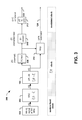
- FIG. 3 is a diagram illustrating a digital front end (DFE) arrangement 306 utilizing zero crossings to generate digital commands for polar modulation in accordance with an embodiment.
- the arrangement 206 and variations thereof can be utilized as the DFE 106 and the like and used in a DTx.
- the arrangement 306 and variations thereof can be utilized as the DFE 106 .
- the arrangement 306 includes a zero crossing (ZC) finder 208 , a pre-distortion component 310 , a zero crossings (ZC) correct component 210 , a ZC to DCT converter 212 and an amplifier 214 .
- the arrangement 206 utilizes a modem 102 , a VRC component 20 and an LPI component 104 . It is appreciated that these components and others can be included as part of the DFE 306 . Additional description for the included components can be found above with regard to FIG. 2 .
- the modem 102 generates a baseband signal having I and Q components at a baseband frequency.
- the VRC (variable rate converter) 203 is configured to resample data of the baseband signal at a rate related to a carrier frequency.
- the VRC 203 uses relatively low power via a low sample rate, based on fractional delay filtering.
- the LPI 104 further reduces the frequency of the baseband signal to generate an interpolated baseband signal.
- the interpolated baseband signal is adjusted to the adjusted frequency of about 2560 MHz from the baseband frequency of 640 MHz.
- the adjusted frequency permits operation and calculation of digital commands with less or reduced power consumption and complexity.
- the interpolated baseband signal is provided to the ZC finder 208 and the power amplifier 214 .
- the interpolated baseband signal is also referred to as a modulated signal.
- the ZC finder 208 is configured to calculate ZC positions of the modulated signal.
- the ZC positions are calculated by coarsely calculating the modulated signal in a high sampling rate, identifying sign changes. Accuracy of the ZC position calculations can be improved with linear interpolation.
- the calculated ZC positions also referred to as a modulated clock, are provided to the amplifier 214 .
- the ZC correct component 310 performs a correction on rising edges of the modulated signal.
- the correction can also be referred to as a pre-distortion.
- the falling edges are in a constant or substantially constant offset of the rising edges.
- the ZC correct component 310 is configured to utilize required falling edges positions and a predetermined or known offset to calculate an expected error of the falling edges. Then, the expected error of the falling edges is used to generate an error for the rising edges. This error is added to the rising edges to obtain a total error with a zero mean, in one example. Thus, the expected error is compensated by adding a negative error on the rising edges to obtain the total error with a zero mean.
- the ZC correct component 310 is configured to utilize required rising edge positions and a known offset to calculate an expected error of the rising edges. Then, the expected error of the rising edges is used to generate an error for the falling edges. The expected error here is compensated for by adding a negative error on the falling edges to obtain a total error with a zero mean.
- the ZC correction component 310 can perform edge correction for rising edges and falling edges as shown above. It is further appreciated that the ZC correction component 310 can also perform edge correction on both rising and falling edges. Performing edge correction on only one of the edges can mitigate power consumption while providing suitable edge correction.
- the ZC to DCT converter 212 is configured to convert the calculated ZC positions, after correction to DTC commands 122 .
- the converter 212 uses a low power implementation where DTC commands are extracted from a ZC delay.
- the extraction is a delay relative to a VCO clock and the ZD delay is relative a digital clock.
- bit selection is used where the digital clock is closely related to the VCO clock.
- An example of the VCO clock is shown above with regard to FIG. 1 and the VCO clock 132 generated by the DPLL 116 .
- the amplifier 214 is configured to generate DPA commands 124 based on the modulated signal from the LPI component 104 and the calculated ZC positions from the ZC finder 208 .
- the amplifier 218 determines or calculates amplitude values at the calculated ZC positions.
- a suitable technique such as linear interpolation of the base-band absolute values, can be utilized.
- the DTC commands 122 and the DPA commands 124 can then be utilized to generate an output signal for transmission as described above.
- FIG. 4 is a diagram illustrating a transceiver arrangement 400 in accordance with an aspect of present disclosure.
- the arrangement 400 utilizes a DTx with a DFE.
- the DFE utilizes zero crossings of a modulated signal to generate digital commands including DPA commands and DTC commands.
- the arrangement 400 is provided as an example for illustrative purposes.
- the arrangement 400 includes a modem 102 , a transmission (TX) chain 424 , a DPLL 116 , a receive (RX) chain 426 and an antenna array 428 . It is appreciated other components can be included.
- the RX chain 426 is configured to receive an incoming or received signal 432 from the antenna array 428 .
- the array 428 includes one or antenna for sending and/or receiving signals.
- the array 428 can include other components including, for example, a duplexer, impedance matching, filters, amplifiers, and the like.
- the RX chain 426 converts and process the received signal 432 to generate a received baseband signal 430 .
- the processing includes mixing, downconverting, demodulation and the like.
- the RX chain 426 can use a local oscillator signal from the DPLL 116 .
- the TX chain 424 receives a baseband signal 118 from the modem 102 and generates an output signal 129 for transmission from the baseband signal 118 .
- the output signal 128 is provided to the antenna array 428 for transmission.
- the TX chain 424 includes a DFE 106 , which can be implemented as the DFE 106 described with regards to FIG. 1 , the DFE 206 described above, and the like.
- the DFE 106 utilizes a VCO signal 132 from the DPLL 116 to generate the output signal 118 .
- the arrangement 400 can be utilized within a mobile communications device, such as a user equipment (UE) and the like.
- UE user equipment
- FIG. 5 is a diagram illustrating an exemplary user equipment or mobile communication device 500 that can be utilized with the one or more embodiments described above.
- the mobile communication device 500 for example, comprises a digital baseband processor 502 that can be coupled to a data store or memory 503 , a front end 504 (e.g., an RF front end, an acoustic front end, or the other like front end) and a plurality of antenna ports 507 for connecting to a plurality of antennas 506 1 to 506 k (k being a positive integer).
- the antennas 506 1 to 506 k can receive and transmit signals to and from one or more wireless devices such as access points, access terminals, wireless ports, routers and so forth, which can operate within a radio access network or other communication network generated via a network device.
- the user equipment 500 can be a radio frequency (RF) device for communicating RF signals, an acoustic device for communicating acoustic signals, or any other signal communication device, such as a computer, a personal digital assistant, a mobile phone or smart phone, a tablet PC, a modem, a notebook, a router, a switch, a repeater, a PC, network device, base station or a like device that can operate to communicate with a network or other device according to one or more different communication protocols or standards.
- RF radio frequency
- the front end 504 can include a communication platform, which comprises electronic components and associated circuitry that provide for processing, manipulation or shaping of the received or transmitted signals via one or more receivers or transmitters 508 , a mux/demux component 512 , and a mod/demod component 514 .
- the one or more transmitters 508 can include a DTx, such as the DTx arrangements described above, which facilitates generation of the transmitted signals.
- the front end 504 is coupled to the digital baseband processor 502 and the set of antenna ports 507 , in which the set of antennas 506 , to 506 k can be part of the front end.
- the user equipment device 500 can also include a processor 502 or a controller that can operate to provide or control one or more components of the mobile device 500 .
- the processor 502 can confer functionality, at least in part, to substantially any electronic component within the mobile communication device 500 , in accordance with aspects of the disclosure.
- the processor 502 can operate to enable the mobile communication device 500 to process data (e.g., symbols, bits, or chips) for multiplexing/demultiplexing with the mux/demux component 512 , or modulation/demodulation via the mod/demod component 514 , such as implementing direct and inverse fast Fourier transforms, selection of modulation rates, selection of data packet formats, inter-packet times, etc.
- data e.g., symbols, bits, or chips
- Memory 503 can store data structures (e.g., metadata), code structure(s) (e.g., modules, objects, classes, procedures, or the like) or instructions, network or device information such as policies and specifications, attachment protocols, code sequences for scrambling, spreading and pilot (e.g., reference signal(s)) transmission, frequency offsets, cell IDs, and other data for detecting and identifying various characteristics related to RF input signals, a power output or other signal components during power generation.
- data structures e.g., metadata
- code structure(s) e.g., modules, objects, classes, procedures, or the like
- instructions e.g., modules, objects, classes, procedures, or the like
- network or device information such as policies and specifications, attachment protocols, code sequences for scrambling, spreading and pilot (e.g., reference signal(s)) transmission, frequency offsets, cell IDs, and other data for detecting and identifying various characteristics related to RF input signals, a power output or other signal components during power generation.
- the processor 502 is functionally and/or communicatively coupled (e.g., through a memory bus) to memory 503 in order to store or retrieve information necessary to operate and confer functionality, at least in part, to communication platform or front end 504 , the power amplifier (PA) system 510 and substantially any other operational aspects of the PA system 510 .
- PA power amplifier
- FIG. 6 is a flow diagram illustrating a method 600 of operating a digital transmitter (DTx) in accordance with an embodiment.
- the method 600 can be used within a transceiver, mobile device and the like for communication purposes and/or other applications.
- the method begins at block 602 , wherein a baseband signal having I and Q components is generated by a modem or other device.
- the baseband signal is a digital Cartesian signal and the I and Q components and/or other modulation are used to convey information on the baseband signal.
- the baseband signal operates at a suitable frequency, such as 320 MHz, 640 MHz, and the like.
- the baseband signal is resampled or sampled into carrier frequency related samples at block 604 .
- a variable rate converter and/or a low power interpolator can be configured to resample or sample the baseband signal into carrier frequency related samples.
- the resampled signal can also include or be referred to as interpolated signal 120 .
- a digital front end calculates and/or locates Zero Crossing positions (ZC) at block 606 .
- ZC positions are calculated by identifying sign changes.
- the positions are calculated by coarsely calculating a signal at a high sampling rate and then identifying sign changes.
- ZC amplitudes are calculated at the calculated ZCs to generate DPA commands at block 608 .
- An amplifier can be used to determine or calculate amplitude values at the identified ZC positions. The amplitude values at the ZC positions are provided as the DPA commands.
- the calculated ZCs are converted to DTC commands at block 610 .
- DTC commands are extracted or obtained from a ZC delay as determined by a ZC to DCT converter, such as the converter 212 .
- the ZC delay is relative to a digital clock and the extraction is obtained relative to a VCO clock and the ZC delay.
- a transmission chain having a DTC component and a DPA component generates an output signal using the DPA commands and the DTC commands at block 612 .
- the DTC component generates a modulated clock based on the VCO signal 132 and the DTC commands 122 .
- the DTC component performs phase modulation using the DTC commands to generate the modulated clock or modulated clock signal.
- the DPA component uses the modulated clock and the DPA commands to generate the output signal.
- the DPA component can include, for example, a class D digital power amplifier (DPA), which is used to generate amplitude modulation.
- the output signal includes phase modulation from the DTC component and amplitude modulation from the DPA component.
- a band pass filter or other similar component can be used to remove unwanted noise and/or unwanted signals from the output signal. Additionally, other processing including filtering, amplification and the like can also be performed.
- the output signal can then be transmitted using one or more antenna, such as by an antenna array.
- the method 600 can be repeated at regular or irregular intervals.
- the claimed subject matter may be implemented as a method, apparatus, or article of manufacture using standard programming and/or engineering techniques to produce software, firmware, hardware, or any combination thereof to control a computer to implement the disclosed subject matter (e.g., the systems shown above, are non-limiting examples of circuits that may be used to implement disclosed methods and/or variations thereof).
- the term “article of manufacture” as used herein is intended to encompass a computer program accessible from any computer-readable device, carrier, or media.
- Examples may include subject matter such as a method, means for performing acts or blocks of the method, at least one machine-readable medium including instructions that, when performed by a machine cause the machine to perform acts of the method or of an apparatus or system for concurrent communication using multiple communication technologies according to embodiments and examples described herein.
- Example 1 is a digital polar transmitter arrangement having a digital front end (DFE) and a transmit chain.
- the DFE is configured to resample a baseband signal relative to a carrier frequency at a carrier frequency related sample rate, calculate zero crossing positions of the resampled signal, generate delay to time converter (DTC) commands based on the zero crossing positions, calculate amplitude values for the zero crossing positions and to generate dynamic phase alignment (DPA) commands based on the amplitude values.
- the transmit chain is configured to generate an output signal having amplitude and phase modulation based on the DTC and DPA commands.
- Example 2 includes the subject matter of Example 1, including or omitting optional elements, where the DFE includes a variable rate converter (VRC) configured to resample the baseband signal.
- VRC variable rate converter
- Example 3 includes the subject matter of any of Examples 1-2, including or omitting optional elements, where the DFE comprises a low power interpolator configured to resample the baseband signal at the carrier frequency related sample rate.
- the DFE comprises a low power interpolator configured to resample the baseband signal at the carrier frequency related sample rate.
- Example 4 includes the subject matter of any of Examples 1-3, including or omitting optional elements, where the DFE comprises a zero crossing finder configured to the zero crossing positions.
- Example 5 includes the subject matter of any of Examples 1-4, including or omitting optional elements, where the DFE comprises a zero crossings correction component configured to apply corrections to rising and/or falling edges of the resampled signal.
- the DFE comprises a zero crossings correction component configured to apply corrections to rising and/or falling edges of the resampled signal.
- Example 6 includes the subject matter of any of Examples 1-5, including or omitting optional elements, where the DFE comprises a power amplifier configured to calculate the amplitude values for the zero crossing positions.
- Example 7 includes the subject matter of any of Examples 1-6, including or omitting optional elements, where the transmit chain comprises a DTC component configured to generate a modulated clock having phase modulation based on the DTC commands and a voltage controlled oscillator signal.
- the transmit chain comprises a DTC component configured to generate a modulated clock having phase modulation based on the DTC commands and a voltage controlled oscillator signal.
- Example 8 includes the subject matter of any of Examples 1-7, including or omitting optional elements, where the transmit chain comprises a DPA component configured generate the output signal having amplitude modulation based on the DPA commands and a modulated clock signal.
- the transmit chain comprises a DPA component configured generate the output signal having amplitude modulation based on the DPA commands and a modulated clock signal.
- Example 9 includes the subject matter of any of Examples 1-8, including or omitting optional elements, where the transmit chain comprises a band pass filter configured to remove noise and unwanted signals from the output signal.
- Example 10 includes the subject matter of any of Examples 1-9, including or omitting optional elements, where the transmit chain comprises a band pass filter configured to remove noise and unwanted signals from the output signal.
- Example 11 is a digital front end (DFE) arrangement having a variable rate converter (VRC), a low power interpolator (LPI), a zero crossing finder, a converter and an amplifier.
- VRC variable rate converter
- LPI low power interpolator
- the variable rate converter (VRC) is configured to resample a baseband signal.
- the low power interpolator (LPI) is configured to interpolate the resampled signal based on a carrier frequency.
- the zero crossing finder is configured to calculate zero crossing positions based on the interpolated signal.
- the converter is configured to convert the zero crossing positions into delay to time (DTC) commands.
- DTC delay to time
- the amplifier is configured to calculate amplitude values of the interpolated signal at the zero crossing positions and generate DPA commands based on the calculated amplitude values.
- Example 12 includes the subject matter of Example 11, including or omitting optional elements, further including a modem configured to generate the baseband signal as a Cartesian signal having in-phase (I) and quadrature (Q) components.
- a modem configured to generate the baseband signal as a Cartesian signal having in-phase (I) and quadrature (Q) components.
- Example 13 includes the subject matter of any of Examples 11-12, including or omitting optional elements, where the VRC and the LPI operate on a carrier frequency related signal.
- Example 14 includes the subject matter of any of Examples 11-13, including or omitting optional elements, where wherein the converter operates at a modulated clock.
- Example 15 includes the subject matter of any of Examples 11-14, including or omitting optional elements, where the converter converts the zero crossing positions using a zero crossing delay and a voltage controlled oscillator clock.
- Example 16 includes the subject matter of any of Examples 11-15, including or omitting optional elements, further including a correction component configured to calculate an edge error based on a signal having the zero crossing positions and apply a compensation based on the calculated edge error to edges of the signal and provide the signal having the applied compensation to the converter.
- a correction component configured to calculate an edge error based on a signal having the zero crossing positions and apply a compensation based on the calculated edge error to edges of the signal and provide the signal having the applied compensation to the converter.
- Example 17 includes the subject matter of any of Examples 11-16, including or omitting optional elements, further including a transmit chain configured to generate an output signal having amplitude and phase modulation based on the DTC and DPA commands.
- Example 18 is a method of operating a digital transmitter.
- a digital baseband signal having inphase (I) and quadrature (Q) components is generated.
- the baseband signal is resampled at a frequency related to a carrier frequency and higher than a baseband frequency of the baseband signal.
- Zero crossing positions are calculated based on the resampled baseband signal having I and Q components.
- the zero crossing positions are converted into delay to time (DTC) commands.
- DTC delay to time
- Example 19 includes the subject matter of Example 18, including or omitting optional elements, further comprising calculating amplitudes values of the resampled baseband signal at the zero crossing positions to generate DPA commands.
- Example 20 includes the subject matter of any of Examples 18-19, including or omitting optional elements, further comprising interpolating the resampled baseband signal prior to calculating the zero crossing positions.
- Example 21 includes the subject matter of any of Examples 18-20, including or omitting optional elements, further comprising generating an output signal having amplitude and phase modulation based on the DTC and DPA commands.
- Example 22 is a digital polar transmitter arrangement having a digital front end (DFE).
- the arrangement comprises a means to resample a baseband signal relative to a carrier frequency at a carrier frequency related sample rate, a means to calculate zero crossing positions of the resampled signal, a means to generate delay to time converter (DTC) commands based on the zero crossing positions, a means to calculate amplitude values for the zero crossing positions and generate dynamic phase alignment (DPA) commands based on the amplitude values, wherein the baseband signal is a digital Cartesian signal having inphase (I) and quadrature (Q) components, and a means to generate an output signal having amplitude and polar modulation for transmission based on the DPA commands and the DTC commands.
- DTC delay to time converter
- DPA dynamic phase alignment
- Example 23 is a digital polar transmitter arrangement.
- the arrangement includes a means for generating a digital baseband signal having inphase (I) and quadrature (Q) components, a means for resampling the baseband signal at a frequency related to a carrier frequency and higher than a baseband frequency of the baseband signal, a means for calculating zero crossing positions based on the resampled baseband signal having I and Q components, and a means for converting the zero crossing positions into delay to time (DTC) commands.
- DTC delay to time
- the terms (including a reference to a “means”) used to describe such components are intended to correspond, unless otherwise indicated, to any component or structure which performs the specified function of the described component (e.g., that is functionally equivalent), even though not structurally equivalent to the disclosed structure which performs the function in the herein illustrated exemplary implementations of the invention.
- the component or structure includes a processer executing instructions in order to perform at least portions of the various functions.
- a particular feature of the invention may have been disclosed with respect to only one of several implementations, such feature may be combined with one or more other features of the other implementations as may be desired and advantageous for any given or particular application.
Landscapes
- Engineering & Computer Science (AREA)
- Computer Networks & Wireless Communication (AREA)
- Signal Processing (AREA)
- Power Engineering (AREA)
- Amplifiers (AREA)
- Digital Transmission Methods That Use Modulated Carrier Waves (AREA)
- Transmitters (AREA)
Abstract
Description
Z(t)=I(t)+j·Q(t)=A(t)·exp(j·φ(t))
Cartesian: Y(t)=I(t)·cos(2π·F c ·t)−Q(t)−sin(2π·F c ·t)
Polar: Y(t)=A(t)·cos(2π·F c ·t+φ(t))
DTx: Y′(t)=A′(t)·sign(cos(2π·F c ·t+φ′(t)))
Y″(t)=BPF{A′(t)·sign(cos(2πF c t+φ′(t)))}≈A(t)*cos(2πF c t+φ(t))=Y(t)
Claims (21)
Priority Applications (2)
| Application Number | Priority Date | Filing Date | Title |
|---|---|---|---|
| US15/382,808 US9912357B1 (en) | 2016-12-19 | 2016-12-19 | Digital polar transmitter having a digital front end |
| PCT/US2017/059195 WO2018118226A1 (en) | 2016-12-19 | 2017-10-31 | Digital polar transmitter having a digital front end |
Applications Claiming Priority (1)
| Application Number | Priority Date | Filing Date | Title |
|---|---|---|---|
| US15/382,808 US9912357B1 (en) | 2016-12-19 | 2016-12-19 | Digital polar transmitter having a digital front end |
Publications (1)
| Publication Number | Publication Date |
|---|---|
| US9912357B1 true US9912357B1 (en) | 2018-03-06 |
Family
ID=60473603
Family Applications (1)
| Application Number | Title | Priority Date | Filing Date |
|---|---|---|---|
| US15/382,808 Expired - Fee Related US9912357B1 (en) | 2016-12-19 | 2016-12-19 | Digital polar transmitter having a digital front end |
Country Status (2)
| Country | Link |
|---|---|
| US (1) | US9912357B1 (en) |
| WO (1) | WO2018118226A1 (en) |
Cited By (3)
| Publication number | Priority date | Publication date | Assignee | Title |
|---|---|---|---|---|
| CN108337639A (en) * | 2018-05-02 | 2018-07-27 | 鹿建银 | A kind of Monte Carlo mobile node location algorithm based on Newton interpolation |
| US10447245B1 (en) | 2018-09-28 | 2019-10-15 | Intel Corporation | Adaptive sample rate reduction for digital IQ transmitters |
| CN113169950A (en) * | 2018-09-07 | 2021-07-23 | 盈诺飞公司 | System and method for upsampling a stream of polar amplitude samples in a polar modulator |
Families Citing this family (2)
| Publication number | Priority date | Publication date | Assignee | Title |
|---|---|---|---|---|
| WO2021024426A1 (en) * | 2019-08-07 | 2021-02-11 | オムロン株式会社 | Noise canceling device for wireless communication system |
| EP4020820A1 (en) | 2020-12-22 | 2022-06-29 | INTEL Corporation | Methods and devices for asymmetric frequency spreading |
Citations (8)
| Publication number | Priority date | Publication date | Assignee | Title |
|---|---|---|---|---|
| US20100061128A1 (en) * | 2007-03-30 | 2010-03-11 | Ryou Nakamoto | Electric power supply circuit |
| US7817747B2 (en) | 2006-02-15 | 2010-10-19 | Texas Instruments Incorporated | Precise delay alignment between amplitude and phase/frequency modulation paths in a digital polar transmitter |
| US7826554B2 (en) | 2006-03-13 | 2010-11-02 | Interdigital Technology Corporation | Digital transmitter |
| US20110129037A1 (en) | 2009-11-30 | 2011-06-02 | Bogdan Staszewski | Digital power amplifier with i/q combination |
| US8009765B2 (en) | 2007-03-13 | 2011-08-30 | Pine Valley Investments, Inc. | Digital polar transmitter |
| US8204107B2 (en) | 2008-04-09 | 2012-06-19 | National Semiconductor Corporation | Bandwidth reduction mechanism for polar modulation |
| US8270273B2 (en) * | 2009-05-20 | 2012-09-18 | Novatek Microelectronics Corp. | Calibration circuit and method thereof for data recovery |
| US20140232309A1 (en) * | 2011-09-30 | 2014-08-21 | Daikin Industries, Ltd. | Power converter |
Family Cites Families (2)
| Publication number | Priority date | Publication date | Assignee | Title |
|---|---|---|---|---|
| US8831159B2 (en) * | 2011-02-09 | 2014-09-09 | Intel Mobile Communications GmbH | AM-PM synchronization unit |
| US9197258B1 (en) * | 2014-06-13 | 2015-11-24 | Intel IP Corporation | System and method for generating a data dependent clock for a DAC in a modulator |
-
2016
- 2016-12-19 US US15/382,808 patent/US9912357B1/en not_active Expired - Fee Related
-
2017
- 2017-10-31 WO PCT/US2017/059195 patent/WO2018118226A1/en not_active Ceased
Patent Citations (8)
| Publication number | Priority date | Publication date | Assignee | Title |
|---|---|---|---|---|
| US7817747B2 (en) | 2006-02-15 | 2010-10-19 | Texas Instruments Incorporated | Precise delay alignment between amplitude and phase/frequency modulation paths in a digital polar transmitter |
| US7826554B2 (en) | 2006-03-13 | 2010-11-02 | Interdigital Technology Corporation | Digital transmitter |
| US8009765B2 (en) | 2007-03-13 | 2011-08-30 | Pine Valley Investments, Inc. | Digital polar transmitter |
| US20100061128A1 (en) * | 2007-03-30 | 2010-03-11 | Ryou Nakamoto | Electric power supply circuit |
| US8204107B2 (en) | 2008-04-09 | 2012-06-19 | National Semiconductor Corporation | Bandwidth reduction mechanism for polar modulation |
| US8270273B2 (en) * | 2009-05-20 | 2012-09-18 | Novatek Microelectronics Corp. | Calibration circuit and method thereof for data recovery |
| US20110129037A1 (en) | 2009-11-30 | 2011-06-02 | Bogdan Staszewski | Digital power amplifier with i/q combination |
| US20140232309A1 (en) * | 2011-09-30 | 2014-08-21 | Daikin Industries, Ltd. | Power converter |
Cited By (5)
| Publication number | Priority date | Publication date | Assignee | Title |
|---|---|---|---|---|
| CN108337639A (en) * | 2018-05-02 | 2018-07-27 | 鹿建银 | A kind of Monte Carlo mobile node location algorithm based on Newton interpolation |
| CN108337639B (en) * | 2018-05-02 | 2019-07-26 | 巢湖学院 | A kind of Monte Carlo mobile node location algorithm based on Newton interpolation |
| CN113169950A (en) * | 2018-09-07 | 2021-07-23 | 盈诺飞公司 | System and method for upsampling a stream of polar amplitude samples in a polar modulator |
| CN113169950B (en) * | 2018-09-07 | 2023-11-03 | 盈诺飞公司 | Upsampling system and method for a stream of polar amplitude samples within a polar modulator |
| US10447245B1 (en) | 2018-09-28 | 2019-10-15 | Intel Corporation | Adaptive sample rate reduction for digital IQ transmitters |
Also Published As
| Publication number | Publication date |
|---|---|
| WO2018118226A1 (en) | 2018-06-28 |
Similar Documents
| Publication | Publication Date | Title |
|---|---|---|
| US9912357B1 (en) | Digital polar transmitter having a digital front end | |
| TWI241793B (en) | Method and apparatus for I/Q mismatch calibration in a receiver | |
| CN106817084B (en) | Apparatus and method for phase synchronization of local oscillators in transceivers | |
| US8693525B2 (en) | Multi-carrier transmitter for wireless communication | |
| US9774364B2 (en) | Interference phase estimate system and method | |
| CN1750531B (en) | Distortion compensation quadrature modulator and radio transmitter | |
| US8666325B2 (en) | Polar feedback receiver for modulator | |
| US9867155B1 (en) | Amplitude-modulation signal and phase-modulation signal delay adjustment for polar transmitter | |
| CN101911511B (en) | Phase noise correction circuit, transmitter, receiver, wireless device, radio communications system and phase noise correcting method | |
| WO2016199041A1 (en) | Adaptive i/q mismatch calibration | |
| CN106165366A (en) | Frequency and Phase Offset Compensation for Modulated Signals Using Symbol Timing Recovery | |
| CN104702306B (en) | Parallel Digital is to time converter architecture | |
| CN105024712A (en) | Unwanted component reduction system | |
| Shaboyan et al. | Frequency and timing synchronization for in-band full-duplex OFDM system | |
| JP2011146979A (en) | Transmission apparatus, radio communication apparatus, and transmission method | |
| JP6325942B2 (en) | Wireless communication apparatus and integrated circuit | |
| US10122477B2 (en) | Transmitter performance calibration systems and methods | |
| US20120275494A1 (en) | Methods and apparatus for digital host-lock mode in a transceiver | |
| Syllaios et al. | Recombination of envelope and phase paths in wideband polar transmitters | |
| KR100891819B1 (en) | Direct sampling wireless receiver and method | |
| JP2008172838A (en) | Wireless transmitter | |
| JP4214635B2 (en) | Digital radio equipment | |
| KR100795559B1 (en) | Apparatus and method for compensating high frequency distortion in wireless system of orthogonal frequency division multiplexing | |
| JP4659621B2 (en) | Wireless transmitter | |
| CN104242922B (en) | Wireless Telecom Equipment and its apparatus for frequency synthesizing |
Legal Events
| Date | Code | Title | Description |
|---|---|---|---|
| AS | Assignment |
Owner name: INTEL IP CORPORATION, CALIFORNIA Free format text: ASSIGNMENT OF ASSIGNORS INTEREST;ASSIGNORS:PARKER, URI;BANIN, ELAN;KERNER, MICHAEL;AND OTHERS;SIGNING DATES FROM 20161229 TO 20170118;REEL/FRAME:041122/0643 |
|
| STCF | Information on status: patent grant |
Free format text: PATENTED CASE |
|
| AS | Assignment |
Owner name: INTEL CORPORATION, CALIFORNIA Free format text: ASSIGNMENT OF ASSIGNORS INTEREST;ASSIGNOR:INTEL IP CORPORATION;REEL/FRAME:056543/0359 Effective date: 20210512 |
|
| FEPP | Fee payment procedure |
Free format text: MAINTENANCE FEE REMINDER MAILED (ORIGINAL EVENT CODE: REM.); ENTITY STATUS OF PATENT OWNER: LARGE ENTITY |
|
| LAPS | Lapse for failure to pay maintenance fees |
Free format text: PATENT EXPIRED FOR FAILURE TO PAY MAINTENANCE FEES (ORIGINAL EVENT CODE: EXP.); ENTITY STATUS OF PATENT OWNER: LARGE ENTITY |
|
| STCH | Information on status: patent discontinuation |
Free format text: PATENT EXPIRED DUE TO NONPAYMENT OF MAINTENANCE FEES UNDER 37 CFR 1.362 |
|
| FP | Lapsed due to failure to pay maintenance fee |
Effective date: 20220306 |