US9905183B2 - Gate driver circuit and display device apply circuit thereof - Google Patents
Gate driver circuit and display device apply circuit thereof Download PDFInfo
- Publication number
- US9905183B2 US9905183B2 US15/000,724 US201615000724A US9905183B2 US 9905183 B2 US9905183 B2 US 9905183B2 US 201615000724 A US201615000724 A US 201615000724A US 9905183 B2 US9905183 B2 US 9905183B2
- Authority
- US
- United States
- Prior art keywords
- transistor
- signal
- node
- terminal
- numbered stage
- Prior art date
- Legal status (The legal status is an assumption and is not a legal conclusion. Google has not performed a legal analysis and makes no representation as to the accuracy of the status listed.)
- Active, expires
Links
- 230000005540 biological transmission Effects 0.000 claims description 32
- 239000003990 capacitor Substances 0.000 claims description 14
- 238000000034 method Methods 0.000 description 18
- 239000004973 liquid crystal related substance Substances 0.000 description 6
- 101000805729 Homo sapiens V-type proton ATPase 116 kDa subunit a 1 Proteins 0.000 description 5
- 101000854879 Homo sapiens V-type proton ATPase 116 kDa subunit a 2 Proteins 0.000 description 5
- 101000854873 Homo sapiens V-type proton ATPase 116 kDa subunit a 4 Proteins 0.000 description 5
- 102100020737 V-type proton ATPase 116 kDa subunit a 4 Human genes 0.000 description 5
- 238000010586 diagram Methods 0.000 description 5
- 238000005516 engineering process Methods 0.000 description 4
- 239000000758 substrate Substances 0.000 description 2
- 230000000694 effects Effects 0.000 description 1
- 238000004519 manufacturing process Methods 0.000 description 1
- 230000000750 progressive effect Effects 0.000 description 1
Images


Classifications
-
- G—PHYSICS
- G09—EDUCATION; CRYPTOGRAPHY; DISPLAY; ADVERTISING; SEALS
- G09G—ARRANGEMENTS OR CIRCUITS FOR CONTROL OF INDICATING DEVICES USING STATIC MEANS TO PRESENT VARIABLE INFORMATION
- G09G3/00—Control arrangements or circuits, of interest only in connection with visual indicators other than cathode-ray tubes
- G09G3/20—Control arrangements or circuits, of interest only in connection with visual indicators other than cathode-ray tubes for presentation of an assembly of a number of characters, e.g. a page, by composing the assembly by combination of individual elements arranged in a matrix no fixed position being assigned to or needed to be assigned to the individual characters or partial characters
- G09G3/34—Control arrangements or circuits, of interest only in connection with visual indicators other than cathode-ray tubes for presentation of an assembly of a number of characters, e.g. a page, by composing the assembly by combination of individual elements arranged in a matrix no fixed position being assigned to or needed to be assigned to the individual characters or partial characters by control of light from an independent source
- G09G3/36—Control arrangements or circuits, of interest only in connection with visual indicators other than cathode-ray tubes for presentation of an assembly of a number of characters, e.g. a page, by composing the assembly by combination of individual elements arranged in a matrix no fixed position being assigned to or needed to be assigned to the individual characters or partial characters by control of light from an independent source using liquid crystals
- G09G3/3611—Control of matrices with row and column drivers
- G09G3/3674—Details of drivers for scan electrodes
- G09G3/3677—Details of drivers for scan electrodes suitable for active matrices only
-
- G—PHYSICS
- G09—EDUCATION; CRYPTOGRAPHY; DISPLAY; ADVERTISING; SEALS
- G09G—ARRANGEMENTS OR CIRCUITS FOR CONTROL OF INDICATING DEVICES USING STATIC MEANS TO PRESENT VARIABLE INFORMATION
- G09G3/00—Control arrangements or circuits, of interest only in connection with visual indicators other than cathode-ray tubes
- G09G3/20—Control arrangements or circuits, of interest only in connection with visual indicators other than cathode-ray tubes for presentation of an assembly of a number of characters, e.g. a page, by composing the assembly by combination of individual elements arranged in a matrix no fixed position being assigned to or needed to be assigned to the individual characters or partial characters
- G09G3/34—Control arrangements or circuits, of interest only in connection with visual indicators other than cathode-ray tubes for presentation of an assembly of a number of characters, e.g. a page, by composing the assembly by combination of individual elements arranged in a matrix no fixed position being assigned to or needed to be assigned to the individual characters or partial characters by control of light from an independent source
- G09G3/36—Control arrangements or circuits, of interest only in connection with visual indicators other than cathode-ray tubes for presentation of an assembly of a number of characters, e.g. a page, by composing the assembly by combination of individual elements arranged in a matrix no fixed position being assigned to or needed to be assigned to the individual characters or partial characters by control of light from an independent source using liquid crystals
- G09G3/3611—Control of matrices with row and column drivers
- G09G3/3696—Generation of voltages supplied to electrode drivers
-
- G—PHYSICS
- G11—INFORMATION STORAGE
- G11C—STATIC STORES
- G11C19/00—Digital stores in which the information is moved stepwise, e.g. shift registers
- G11C19/28—Digital stores in which the information is moved stepwise, e.g. shift registers using semiconductor elements
-
- H—ELECTRICITY
- H01—ELECTRIC ELEMENTS
- H01L—SEMICONDUCTOR DEVICES NOT COVERED BY CLASS H10
- H01L27/00—Devices consisting of a plurality of semiconductor or other solid-state components formed in or on a common substrate
- H01L27/02—Devices consisting of a plurality of semiconductor or other solid-state components formed in or on a common substrate including semiconductor components specially adapted for rectifying, oscillating, amplifying or switching and having potential barriers; including integrated passive circuit elements having potential barriers
- H01L27/12—Devices consisting of a plurality of semiconductor or other solid-state components formed in or on a common substrate including semiconductor components specially adapted for rectifying, oscillating, amplifying or switching and having potential barriers; including integrated passive circuit elements having potential barriers the substrate being other than a semiconductor body, e.g. an insulating body
- H01L27/1214—Devices consisting of a plurality of semiconductor or other solid-state components formed in or on a common substrate including semiconductor components specially adapted for rectifying, oscillating, amplifying or switching and having potential barriers; including integrated passive circuit elements having potential barriers the substrate being other than a semiconductor body, e.g. an insulating body comprising a plurality of TFTs formed on a non-semiconducting substrate, e.g. driving circuits for AMLCDs
- H01L27/124—Devices consisting of a plurality of semiconductor or other solid-state components formed in or on a common substrate including semiconductor components specially adapted for rectifying, oscillating, amplifying or switching and having potential barriers; including integrated passive circuit elements having potential barriers the substrate being other than a semiconductor body, e.g. an insulating body comprising a plurality of TFTs formed on a non-semiconducting substrate, e.g. driving circuits for AMLCDs with a particular composition, shape or layout of the wiring layers specially adapted to the circuit arrangement, e.g. scanning lines in LCD pixel circuits
-
- H—ELECTRICITY
- H01—ELECTRIC ELEMENTS
- H01L—SEMICONDUCTOR DEVICES NOT COVERED BY CLASS H10
- H01L27/00—Devices consisting of a plurality of semiconductor or other solid-state components formed in or on a common substrate
- H01L27/02—Devices consisting of a plurality of semiconductor or other solid-state components formed in or on a common substrate including semiconductor components specially adapted for rectifying, oscillating, amplifying or switching and having potential barriers; including integrated passive circuit elements having potential barriers
- H01L27/12—Devices consisting of a plurality of semiconductor or other solid-state components formed in or on a common substrate including semiconductor components specially adapted for rectifying, oscillating, amplifying or switching and having potential barriers; including integrated passive circuit elements having potential barriers the substrate being other than a semiconductor body, e.g. an insulating body
- H01L27/1214—Devices consisting of a plurality of semiconductor or other solid-state components formed in or on a common substrate including semiconductor components specially adapted for rectifying, oscillating, amplifying or switching and having potential barriers; including integrated passive circuit elements having potential barriers the substrate being other than a semiconductor body, e.g. an insulating body comprising a plurality of TFTs formed on a non-semiconducting substrate, e.g. driving circuits for AMLCDs
- H01L27/1255—Devices consisting of a plurality of semiconductor or other solid-state components formed in or on a common substrate including semiconductor components specially adapted for rectifying, oscillating, amplifying or switching and having potential barriers; including integrated passive circuit elements having potential barriers the substrate being other than a semiconductor body, e.g. an insulating body comprising a plurality of TFTs formed on a non-semiconducting substrate, e.g. driving circuits for AMLCDs integrated with passive devices, e.g. auxiliary capacitors
-
- G—PHYSICS
- G09—EDUCATION; CRYPTOGRAPHY; DISPLAY; ADVERTISING; SEALS
- G09G—ARRANGEMENTS OR CIRCUITS FOR CONTROL OF INDICATING DEVICES USING STATIC MEANS TO PRESENT VARIABLE INFORMATION
- G09G2300/00—Aspects of the constitution of display devices
- G09G2300/04—Structural and physical details of display devices
- G09G2300/0404—Matrix technologies
- G09G2300/0408—Integration of the drivers onto the display substrate
-
- G—PHYSICS
- G09—EDUCATION; CRYPTOGRAPHY; DISPLAY; ADVERTISING; SEALS
- G09G—ARRANGEMENTS OR CIRCUITS FOR CONTROL OF INDICATING DEVICES USING STATIC MEANS TO PRESENT VARIABLE INFORMATION
- G09G2300/00—Aspects of the constitution of display devices
- G09G2300/08—Active matrix structure, i.e. with use of active elements, inclusive of non-linear two terminal elements, in the pixels together with light emitting or modulating elements
- G09G2300/0809—Several active elements per pixel in active matrix panels
-
- G—PHYSICS
- G09—EDUCATION; CRYPTOGRAPHY; DISPLAY; ADVERTISING; SEALS
- G09G—ARRANGEMENTS OR CIRCUITS FOR CONTROL OF INDICATING DEVICES USING STATIC MEANS TO PRESENT VARIABLE INFORMATION
- G09G2310/00—Command of the display device
- G09G2310/02—Addressing, scanning or driving the display screen or processing steps related thereto
- G09G2310/0202—Addressing of scan or signal lines
-
- G—PHYSICS
- G09—EDUCATION; CRYPTOGRAPHY; DISPLAY; ADVERTISING; SEALS
- G09G—ARRANGEMENTS OR CIRCUITS FOR CONTROL OF INDICATING DEVICES USING STATIC MEANS TO PRESENT VARIABLE INFORMATION
- G09G2310/00—Command of the display device
- G09G2310/02—Addressing, scanning or driving the display screen or processing steps related thereto
- G09G2310/0224—Details of interlacing
-
- G—PHYSICS
- G09—EDUCATION; CRYPTOGRAPHY; DISPLAY; ADVERTISING; SEALS
- G09G—ARRANGEMENTS OR CIRCUITS FOR CONTROL OF INDICATING DEVICES USING STATIC MEANS TO PRESENT VARIABLE INFORMATION
- G09G2310/00—Command of the display device
- G09G2310/02—Addressing, scanning or driving the display screen or processing steps related thereto
- G09G2310/0264—Details of driving circuits
- G09G2310/0281—Arrangement of scan or data electrode driver circuits at the periphery of a panel not inherent to a split matrix structure
-
- G—PHYSICS
- G09—EDUCATION; CRYPTOGRAPHY; DISPLAY; ADVERTISING; SEALS
- G09G—ARRANGEMENTS OR CIRCUITS FOR CONTROL OF INDICATING DEVICES USING STATIC MEANS TO PRESENT VARIABLE INFORMATION
- G09G2310/00—Command of the display device
- G09G2310/02—Addressing, scanning or driving the display screen or processing steps related thereto
- G09G2310/0264—Details of driving circuits
- G09G2310/0283—Arrangement of drivers for different directions of scanning
-
- G—PHYSICS
- G09—EDUCATION; CRYPTOGRAPHY; DISPLAY; ADVERTISING; SEALS
- G09G—ARRANGEMENTS OR CIRCUITS FOR CONTROL OF INDICATING DEVICES USING STATIC MEANS TO PRESENT VARIABLE INFORMATION
- G09G2310/00—Command of the display device
- G09G2310/02—Addressing, scanning or driving the display screen or processing steps related thereto
- G09G2310/0264—Details of driving circuits
- G09G2310/0286—Details of a shift registers arranged for use in a driving circuit
Definitions
- the present disclosure relates to a display technical field, and in particular to a gate driver circuit and a display device including said gate driver circuit.
- the driver (namely gate driver) of present active liquid crystal display panel horizontal scan line is mainly accomplished by an external IC, integrated circuit, the external IC can control the approximate charge and discharge of each stage of horizontal scan line.
- GOA gate driver on array
- GOA technology is namely array substrate driving technology, can use the original process of liquid crystal display panel to produce the driver circuit of horizontal scan line on the substrate around the display region, in order to alternate the external IC to accomplish the driver of horizontal scan line.
- GOA technology can reduce bonding process of the external IC, it has the opportunity to improve productivity and reduces production costs, and makes liquid crystal display panel more suitable for narrow border of non-border display product.
- the scan method of prior gate driver circuit is generally simple, which commonly carries on forward scanning or reverse scanning at the same time, it can only be progressive or interlaced scanning at the same time, therefore, it needs to improve the prior gate driver circuit, in order to achieve the diversification of the gate scan method, to meet the requirements of different display products.
- the technical issue to be mainly solved by the present disclosure is to improve the prior gate driver circuit, in order to achieve diversification of gate scanning method, to meet the needs of different display products.
- a gate driver circuit which includes:
- each GOA circuit includes:
- a startup module said startup module including a first scan signal terminal in order to receive a first scan signal, a second scan signal terminal in order to receive a second scan signal, a first transistor and a second transistor, wherein first terminal of said first transistor receives a first transmission signal, second terminal of said first transistor receives said first scan signal, first terminal of said second transistor receives a second transmission signal, second terminal of said second transistor receives a second scan signal, third terminals of said first transistor and said transistor are connect with a first node;
- a driving module including a first capacitor, a second capacitor, a third transistor, a fourth transistor, a fifth transistor and a sixth transistor, also including a first timing signal terminal in order to receive a first timing signal, first terminal of said third transistor being connected with said first timing signal terminal, second terminal of said third transistor being connected with said first node, third terminal of said third transistor being connected with second terminal of said fourth transistor, first terminal of said fourth transistor being connected with a second node, third terminal of said fourth transistor being connected with a high voltage input terminal to receive a high voltage signal, said second node being connected with said high voltage input terminal through said second capacitor, said second node being also connected with first terminal of said sixth transistor, second terminal of said sixth transistor being connected with a third node, third terminal of said sixth transistor being connected with said high voltage input terminal to receive said high voltage signal, said third node being connected with said first node through said first capacitor, first terminal of said fifth transistor being connected with said first node, second terminal of said fifth transistor being connected with said first timing signal terminal, third terminal
- control module including a second timing signal terminal, a seventh transistor and a eighth transistor, said second timing signal terminal being used to provide a second timing signal, first terminal of said eighth transistor being connected with a first node, second terminal of said eighth transistor being connected with said second timing signal terminal, third terminal of said eighth transistor being connected with said second node; first terminal of said seventh transistor being connected with said second timing signal terminal, second terminal of said seventh transistor being connected with a low voltage input terminal to receive a low voltage signal, third terminal of said seventh transistor being connected with said second node.
- said gate driver circuit carrying on forward scanning, said first scan signal being low, said second scan signal being high, when said first transmission signal being low, said first transistor turning on, said first scan signal pulling down said first node to low potential, said first transistor transmitting said first scan signal to said first node; at the mean time, said seventh transistor and said eighth transistor turning on, pulling down said second node to low potential; said first timing signal being low at this time, being controlled by said first node, said fifth transistor turning on, being controlled by said second node, said fourth transistor and said sixth transistor turning on, said third node being high.
- said gate driver circuit carrying on reverse scanning, said first scan signal being high, said second scan signal being low, said second transistor turning on, said first scan signal pulling down said first node to low potential, said first transistor transmitting said first scan signal to said first node; at the mean time, said seventh transistor and said eighth transistor turning on, pulling down said second node to low potential; said first timing signal being low at this time, being controlled by said first node, said fifth transistor turning on, being controlled by said second node, said fourth transistor and said sixth transistor turning on, said third node being high.
- said gate driver circuit controlling odd-numbered stage GOA circuit and even-numbered stage GOA circuit to simultaneously carry on forward scanning or reverse scanning through controlling potentials of odd-numbered stage scan signal and odd-numbered stage scan signal and coordinating with odd-numbered stage startup signal and even-numbered stage startup signal with different timing.
- said gate driver circuit controlling odd-numbered stage GOA circuit and even-numbered stage GOA circuit to respectively carry on forward scanning or reverse scanning through controlling potentials of odd-numbered stage scan signal and odd-numbered stage scan signal and coordinating with odd-numbered stage startup signal and even-numbered stage startup signal with different timing.
- the other technical solution adopted by the present disclosure is: to provide a display device, said display device includes any one of gate driver circuits described above.
- the benefit effect of present disclosure is: to distinguish to the situation of prior art, the gate driver circuit provided by the present disclosure to cascade each of the odd-numbered stage GOA circuit, to cascade each even-numbered stage GOA circuit; corresponding to said odd-numbered stage GOA provides an odd-numbered stage scan signal, and odd-numbered stage startup signal, an odd-numbered stage timing signal; corresponding to said even-numbered stage GOA circuit provides an even-numbered stage scan signal, an even-numbered stage startup signal, an even-numbered stage timing signal; through controlling the potential of odd-numbered stage scan signal and even-numbered stage scan signal, coordinating with odd-numbered stage startup signal and even-numbered stage startup signal with different timing, it can control odd-numbered stage GOA circuit and even-numbered stage GOA circuit to respectively carry on forward scanning or reverse scanning, to achieve diversification of gate scanning method, improve the display quality, to meet the needs of different display products.
- FIG. 1 is a structure schematic diagram of a preferred embodiment of a gate driver circuit which is applied to a liquid crystal display device of the present disclosure
- FIG. 2 is a schematic diagram of different scanning method of a preferred embodiment of a gate driver circuit of the present disclosure
- FIG. 3 is a schematic diagram of different scanning method corresponding to the control signal in FIG. 2 ;
- FIG. 4 is a circuit diagram of a preferred embodiment of a gate driver circuit of the present disclosure.
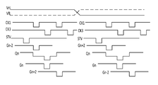
- FIG. 5 is a timing chart of a preferred embodiment of a gate driver circuit of the present disclosure.
- FIG. 1 is a structure schematic diagram of a gate driver circuit 100 which is applied to a liquid crystal display device 200 .
- Left and right sides of apture area, AA, of the liquid crystal display device 200 are provided a GOA circuit.
- left side GOA circuit is odd-numbered stage GOA circuit
- right side GOA circuit is even-numbered stage GOA circuit.
- the gate driver circuit 100 of the present disclosure includes a plurality GOA circuits, wherein each odd-numbered stage GOA circuit cascades, each even-numbered stage GOA circuit cascades. Said gate driver circuit 100 also includes signal lines corresponding to said odd-numbered stage GOA provides an odd-numbered stage scan signal, and odd-numbered stage startup signal, an odd-numbered stage timing signal; signal lines corresponding to said even-numbered stage GOA circuit provides an even-numbered stage scan signal, an even-numbered stage startup signal, an even-numbered stage timing signal.
- said odd-numbered GOA circuit is controlled by a scan signal VfL, a scan signal VrL to carry on forward and reverse scanning.
- said even-numbered GOA circuit is controlled by a scan signal VfR, a scan signal VrR to carry on forward and reverse scanning.
- each stage of GOA circuit includes a startup module 10 , a driving module 11 and a control module 12 .
- Said startup module 10 includes a scan signal terminal VfL to receive the scan signal VfL, a scan signal terminal VrL to receive a scan signal VrL, a transistor T 2 and a transistor T 9 .
- first terminal of said transistor T 2 receives a transmission signal Gn ⁇ 2 from (n ⁇ 2)th stage GOA circuit
- second terminal of said transistor T 2 receives said scan signal VfL
- first terminal of said transistor T 9 receives a transmission signal Gn+ 2 from (n+2)th stage GOA circuit
- second terminal of said transistor T 9 receives said scan signal VrL.
- Third terminals of said transistor T 2 and said transistor T 9 are connected with a first node Qn.
- Said driving module 11 includes a capacitor C 1 , a capacitor C 2 , a transistor T 4 , a transistor T 5 , a transistor T 6 and a transistor T 7 , also includes a timing signal terminal CK to receives a timing signal CK 3 .
- First terminal of said transistor T 4 is connected with said timing signal terminal CK
- second terminal of said transistor T 4 is connected with a first node Qn
- third terminal of said transistor T 4 is connected with second terminal of said transistor T 5 .
- First terminal of said transistor T 5 is connected with a second node Pn
- third terminal of said transistor T 5 is connected with a high voltage input terminal VGH.
- Said second node Pn is connected with said high voltage input terminal VGH through said capacitor C 2 .
- Said second node Pn is also connected with first terminal of said transistor T 7 , second terminal of said transistor T 7 is connected with third node Gn, third terminal of said transistor T 7 is connected with said high voltage input terminal VGH.
- Said third node Gn is connected with said first node Qn through said capacitor C 1 .
- First terminal of said transistor T 6 is connected with said first node Qn, second terminal of said transistor T 6 is connected with said timing signal terminal CK, third terminal of said transistor T 6 is connected with said third node Gn.
- Said control module 12 includes a timing signal terminal XCK, a transistor T 1 , a transistor T 3 and a low voltage input terminal VGL.
- Said timing signal terminal XCK is used to provide a timing signal CK 1 .
- First terminal of said transistor T 3 is connected with said first node Qn
- second terminal of said transistor T 3 is connected with said timing signal XCK
- third terminal of said transistor T 3 is connected with said second node Pn.
- First terminal of said transistor T 1 is connected with said timing signal terminal XCK
- second terminal of said transistor T 1 is connected with said low voltage input terminal VGL
- third terminal of said transistor T 1 is connected with said second node Pn.
- the specific process of carrying on forward scanning of odd-numbered stage GOA circuit of the gate driver circuit 100 of the present disclosure is: said scan signal VfL is low, said scan signal VrL is high, Nth stage GOA circuit receives a transmission signal Gn ⁇ 2 from (n ⁇ 2)th stage GOA circuit, when the transmission signal Gn ⁇ 2 of (N ⁇ 2)th stage GOA circuit is low, said transistor T 2 turns on, said scan signal VfL pulls down said first node Qn to low potential, said transistor T 2 transmits said scan signal VfL to said first node Qn at this time; at the mean time, said transistor T 3 and said transistor T 1 turn on, to pull down said second node Pn to low potential; said timing signal CK 3 is high at this time, said transistor T 6 controlled by said first node Qn turns on, said transistor T 5 and said transistor T 7 controlled by said second node Pn turns on, said scan signal Gn is high.
- said transmission signal Gn ⁇ 2 of (N ⁇ 2)th stage GOA circuit becomes high, said transistor T 2 turns off, said timing signal CK 3 becomes low, said timing signal CK 1 is high, said third node Gn output low voltage signal to drive AA region pixel unit as a transmission signal of a subordinate (Gn+ 2 ).
- Said transistor T 3 turns on, said second node Pn becomes high through XCK, said transistor T 5 and said transistor T 7 turns off, said first node Pn keeps high potential through said capacitor C 1 to ensure that said third node Gn keeps on to output low voltage signal.
- Gn+ 2 becomes low, said transistor T 9 turns on, said first node Qn is pulled up to high potential, said timing signal CK 1 is low, said second node Pn becomes low, said transistor T 5 and said transistor T 7 turns on, said third node Gn is now.
- said timing signal CK 3 is low, said transistor T 5 turns on, said first node Qn is pulled up to high potential, and said first node Qn keeps high potential in the remaining time of one frame, said second node Pn keeps low.
- odd-numbered stage GOA circuit of the gate driver circuit 100 of the present disclosure is: said scan signal VfL is high, said scan signal VrL is low, Nth stage GOA circuit receives said transmission signal Gn+ 2 from (N+2)th stage GOA circuit, when said transmission signal Gn+ 2 of (N+2)th stage GOA circuit is low, said transistor T 9 turns on, said scan signal VrL pulls down said first node Qn to low potential, said transistor T 9 transmits said scan signal VrL to said first node Qn at this time; at the mean time, said transistor T 3 and said transistor T 1 turns on, to pull down said third node Pn to low potential; said timing signal CK 3 is high at this time, being controlled by said first node Qn, said transistor T 6 turns on, being controlled by said second node Pn, said transistor T 5 and said transistor T 7 turns on, said scan signal Gn is high.
- said transmission signal Gn+ 2 of (N+2)th stage GOA circuit becomes high, said transistor T 9 turns off, said timing signal CK 3 becomes low, said timing signal CK 1 is high, said third node Gn outputs low voltage signal to drive AA region pixel unit as a subordinate (Gn ⁇ 2 ) transmission signal.
- Said transistor T 3 turns on, second node Pn becomes high through XCK, said transistor T 5 and said transistor T 7 turns off, said first node Qn keeps high potential through said capacitor C 1 to ensure said third node Gn to keep on outputting low voltage signal.
- Gn ⁇ 2 becomes low, said transistor T 9 turns on, said first node Qn is pulled up to high potential, said timing signal CK 1 is low, said second node Pn becomes low, said transistor T 5 and said transistor T 7 turns on, said third node Gn is low.
- said timing signal CK 3 is low, said transistor T 5 turns on, said first node Qn is pulled to high potential, and said first node Qn keeps high potential in remaining time of one frame, said second node Pn keeps low.
- the gate driver circuit 100 of the present disclosure can simultaneously carry on forward scanning and reverse scanning of odd-numbered stage GOA circuit and even-numbered stage GOA circuit, wherein table 2 shows four kinds of scan mode, 00 represents odd and even columns carry on forward scanning, 01 represents odd column carrying on forward scanning, even column carrying on reverse scanning; 11 represents odd and even columns carry on reverse scanning, 10 represents odd column carry on reverse scanning even column carry on forward scanning.
- Table 3 is the required potential of control signal to achieve the above method.
- said odd-numbered stage GOA circuit reverse scanning and said even-numbered stage GOA circuit reverse scanning are simultaneously carried on.
- said scan signal VfL and said scan signal VfR are high, said scan signal VrL and said scan signal VrR are low; when a frame scanning begins, to provide a startup signal STV 1 to the gate of said transistor T 2 of said first stage GOA circuit, to provide a startup signal STV 2 to the gate of said transistor T 2 of said second stage GOA circuit at the same time (the timing is same as STV 1 , but output from IC, to be marked as STV in FIG. 5 ).
- said odd-numbered stage GOA circuit forward scanning and said even-numbered stage GOA circuit forward scanning are simultaneously carried on.
- said scan signal VfL and said scan signal VfR are low, said scan signal VrL and said scan signal VrR are high; when a frame scanning begins, to provide a startup signal STV 2 to the gate of said transistor T 9 of said last second stage GOA circuit, to provide a startup signal STV 1 to the gate of said transistor T 9 of said last stage GOA circuit.
- said odd-numbered stage GOA circuit reverse scanning and said even-numbered stage GOA circuit forward scanning are simultaneously carried on.
- said scan signal VfL and said scan signal VrR are high, said scan signal VrL and said scan signal VfR are low; when a frame scanning begins, to provide a startup signal STV 1 to the gate of said transistor T 2 of said first stage GOA circuit, to provide a startup signal STV 2 to the gate of said transistor T 9 of said last stage GOA circuit.
- said odd-numbered stage GOA circuit forward scanning and said even-numbered stage GOA circuit reverse scanning are simultaneously carried on.
- said scan signal VfL and said scan signal VrR are low, said scan signal VrL and said scan signal VfR are high; when a frame scanning begins, to provide a startup signal STV 2 to the gate of said transistor T 9 of said last second stage GOA circuit, to provide a startup signal STV 1 to the gate of said transistor T 2 of said second stage GOA circuit.
- the gate driver circuit of the present disclosure can be respectively carried on forward scanning or reverse scanning of odd-numbered GOA circuit and even-numbered stage GOA circuit, similar to above process, there is no more description.
- the transistors of the gate driver circuit of the present disclosure are described as a P-channel FET, first terminal of the transistor corresponds to the gate of FET, second terminal of the transistor corresponds to the drain of FET, third terminal of the transistor corresponds to the source of FET. It should be realized that the transistor of the gate driver circuit of the present disclosure could also choose other types of FET.
- the gate driver circuit 100 of the present disclosure cascades each odd-numbered stage GOA circuit, cascades each even-numbered stage GOA circuit; corresponding to said odd-numbered stage GOA provides an odd-numbered stage scan signal, and odd-numbered stage startup signal, an odd-numbered stage timing signal; corresponding to said even-numbered stage GOA circuit provides an even-numbered stage scan signal, an even-numbered stage startup signal, an even-numbered stage timing signal; through controlling the potential of odd-numbered stage scan signal and even-numbered stage scan signal, coordinating with odd-numbered stage startup signal and even-numbered stage startup signal with different timing, it can control odd-numbered stage GOA circuit and even-numbered stage GOA circuit to respectively carry on forward scanning or reverse scanning, to achieve diversification of gate scanning method, improve the display quality, to meet the needs of different display products.
Landscapes
- Engineering & Computer Science (AREA)
- Physics & Mathematics (AREA)
- Computer Hardware Design (AREA)
- General Physics & Mathematics (AREA)
- Power Engineering (AREA)
- Chemical & Material Sciences (AREA)
- Crystallography & Structural Chemistry (AREA)
- Theoretical Computer Science (AREA)
- Condensed Matter Physics & Semiconductors (AREA)
- Microelectronics & Electronic Packaging (AREA)
- Control Of Indicators Other Than Cathode Ray Tubes (AREA)
- Liquid Crystal Display Device Control (AREA)
Abstract
The present disclosure provides a gate driver circuit, which cascades each even-numbered stage GOA circuit; corresponding to said odd-numbered stage GOA provides an odd-numbered stage scan signal, and odd-numbered stage startup signal, an odd-numbered stage timing signal; corresponding to said even-numbered stage GOA circuit provides an even-numbered stage scan signal, an even-numbered stage startup signal, an even-numbered stage timing signal; through controlling the potential of odd-numbered stage scan signal and even-numbered stage scan signal, coordinating with odd-numbered stage startup signal and even-numbered stage startup signal with different timing, it can control odd-numbered stage GOA circuit and even-numbered stage GOA circuit to respectively carry on forward scanning or reverse scanning. The present disclosure also provides a display device applying said gate driver circuit.
Description
1. Field of the Disclosure
The present disclosure relates to a display technical field, and in particular to a gate driver circuit and a display device including said gate driver circuit.
2. The Related Arts
The driver (namely gate driver) of present active liquid crystal display panel horizontal scan line is mainly accomplished by an external IC, integrated circuit, the external IC can control the approximate charge and discharge of each stage of horizontal scan line. However, GOA (gate driver on array) technology is namely array substrate driving technology, can use the original process of liquid crystal display panel to produce the driver circuit of horizontal scan line on the substrate around the display region, in order to alternate the external IC to accomplish the driver of horizontal scan line. GOA technology can reduce bonding process of the external IC, it has the opportunity to improve productivity and reduces production costs, and makes liquid crystal display panel more suitable for narrow border of non-border display product. The scan method of prior gate driver circuit is generally simple, which commonly carries on forward scanning or reverse scanning at the same time, it can only be progressive or interlaced scanning at the same time, therefore, it needs to improve the prior gate driver circuit, in order to achieve the diversification of the gate scan method, to meet the requirements of different display products.
The technical issue to be mainly solved by the present disclosure is to improve the prior gate driver circuit, in order to achieve diversification of gate scanning method, to meet the needs of different display products.
In order to solve the above issue, a technical solution adopted by the present disclosure is:
A gate driver circuit, which includes:
a plurality of GOA circuits, wherein each of the odd-numbered stage GOA circuit cascades, each even-numbered stage GOA circuit cascades; corresponding to said odd-numbered stage GOA being used to provide signal lines of an odd-numbered stage first scan signal, an odd-numbered stage second scan signal, and odd-numbered stage startup signal, an odd-numbered stage first timing signal, an odd-numbered stage second timing signal; corresponding to said even-numbered stage GOA circuit being used to provide signal lines of an even-numbered stage first scan signal, an even-numbered stage second scan signal, an even-numbered stage startup signal, an even-numbered stage first timing signal, an even-numbered stage second timing signal;
wherein each GOA circuit includes:
a startup module, said startup module including a first scan signal terminal in order to receive a first scan signal, a second scan signal terminal in order to receive a second scan signal, a first transistor and a second transistor, wherein first terminal of said first transistor receives a first transmission signal, second terminal of said first transistor receives said first scan signal, first terminal of said second transistor receives a second transmission signal, second terminal of said second transistor receives a second scan signal, third terminals of said first transistor and said transistor are connect with a first node;
a driving module, said driving module including a first capacitor, a second capacitor, a third transistor, a fourth transistor, a fifth transistor and a sixth transistor, also including a first timing signal terminal in order to receive a first timing signal, first terminal of said third transistor being connected with said first timing signal terminal, second terminal of said third transistor being connected with said first node, third terminal of said third transistor being connected with second terminal of said fourth transistor, first terminal of said fourth transistor being connected with a second node, third terminal of said fourth transistor being connected with a high voltage input terminal to receive a high voltage signal, said second node being connected with said high voltage input terminal through said second capacitor, said second node being also connected with first terminal of said sixth transistor, second terminal of said sixth transistor being connected with a third node, third terminal of said sixth transistor being connected with said high voltage input terminal to receive said high voltage signal, said third node being connected with said first node through said first capacitor, first terminal of said fifth transistor being connected with said first node, second terminal of said fifth transistor being connected with said first timing signal terminal, third terminal of said transistor being connected with said third node;
a control module, said control module including a second timing signal terminal, a seventh transistor and a eighth transistor, said second timing signal terminal being used to provide a second timing signal, first terminal of said eighth transistor being connected with a first node, second terminal of said eighth transistor being connected with said second timing signal terminal, third terminal of said eighth transistor being connected with said second node; first terminal of said seventh transistor being connected with said second timing signal terminal, second terminal of said seventh transistor being connected with a low voltage input terminal to receive a low voltage signal, third terminal of said seventh transistor being connected with said second node.
Wherein when said gate driver circuit carrying on forward scanning, said first scan signal being low, said second scan signal being high, when said first transmission signal being low, said first transistor turning on, said first scan signal pulling down said first node to low potential, said first transistor transmitting said first scan signal to said first node; at the mean time, said seventh transistor and said eighth transistor turning on, pulling down said second node to low potential; said first timing signal being low at this time, being controlled by said first node, said fifth transistor turning on, being controlled by said second node, said fourth transistor and said sixth transistor turning on, said third node being high.
Wherein when said first transmission signal being high, said first transistor turning off, said first timing signal becoming low, said second timing signal being high, said third node outputting low voltage signal to drive a pixel unit and as a subordinate level transmission signal.
Wherein when said second transmission signal becoming low, said second transistor turning on, said first node being pulled up to high potential, said second timing signal being low, said second node becoming low, said fourth transistor and said sixth transistor turning on, said third node outputting low voltage signal to drive a pixel signal and as a subordinate level transmission signal.
Wherein when said gate driver circuit carrying on reverse scanning, said first scan signal being high, said second scan signal being low, said second transistor turning on, said first scan signal pulling down said first node to low potential, said first transistor transmitting said first scan signal to said first node; at the mean time, said seventh transistor and said eighth transistor turning on, pulling down said second node to low potential; said first timing signal being low at this time, being controlled by said first node, said fifth transistor turning on, being controlled by said second node, said fourth transistor and said sixth transistor turning on, said third node being high.
Wherein when said second transmission signal becoming high, said second transistor turning off, said first timing signal becoming low, said second timing signal being high, said third node outputting low voltage signal to drive a pixel unit and as a subordinate level transmission signal.
Wherein when said first transmission signal becoming low, said first transistor turning on, said first node being pulled up to high potential, said second timing signal being low potential, said second node becoming low, said fourth transistor and said sixth transistor turning on, said third node outputting low voltage signal to drive a pixel unit and as a subordinate level transmission signal.
Wherein said gate driver circuit controlling odd-numbered stage GOA circuit and even-numbered stage GOA circuit to simultaneously carry on forward scanning or reverse scanning through controlling potentials of odd-numbered stage scan signal and odd-numbered stage scan signal and coordinating with odd-numbered stage startup signal and even-numbered stage startup signal with different timing.
Wherein said gate driver circuit controlling odd-numbered stage GOA circuit and even-numbered stage GOA circuit to respectively carry on forward scanning or reverse scanning through controlling potentials of odd-numbered stage scan signal and odd-numbered stage scan signal and coordinating with odd-numbered stage startup signal and even-numbered stage startup signal with different timing.
In order to solve above technical issue, the other technical solution adopted by the present disclosure is: to provide a display device, said display device includes any one of gate driver circuits described above.
The benefit effect of present disclosure is: to distinguish to the situation of prior art, the gate driver circuit provided by the present disclosure to cascade each of the odd-numbered stage GOA circuit, to cascade each even-numbered stage GOA circuit; corresponding to said odd-numbered stage GOA provides an odd-numbered stage scan signal, and odd-numbered stage startup signal, an odd-numbered stage timing signal; corresponding to said even-numbered stage GOA circuit provides an even-numbered stage scan signal, an even-numbered stage startup signal, an even-numbered stage timing signal; through controlling the potential of odd-numbered stage scan signal and even-numbered stage scan signal, coordinating with odd-numbered stage startup signal and even-numbered stage startup signal with different timing, it can control odd-numbered stage GOA circuit and even-numbered stage GOA circuit to respectively carry on forward scanning or reverse scanning, to achieve diversification of gate scanning method, improve the display quality, to meet the needs of different display products.
Following combines the drawings and embodiments to describe the present disclosure in detail.
Refer to FIGS. 1-5 , FIG. 1 is a structure schematic diagram of a gate driver circuit 100 which is applied to a liquid crystal display device 200. Left and right sides of apture area, AA, of the liquid crystal display device 200 are provided a GOA circuit. In the present embodiment, left side GOA circuit is odd-numbered stage GOA circuit, right side GOA circuit is even-numbered stage GOA circuit.
The gate driver circuit 100 of the present disclosure includes a plurality GOA circuits, wherein each odd-numbered stage GOA circuit cascades, each even-numbered stage GOA circuit cascades. Said gate driver circuit 100 also includes signal lines corresponding to said odd-numbered stage GOA provides an odd-numbered stage scan signal, and odd-numbered stage startup signal, an odd-numbered stage timing signal; signal lines corresponding to said even-numbered stage GOA circuit provides an even-numbered stage scan signal, an even-numbered stage startup signal, an even-numbered stage timing signal.
Wherein said odd-numbered GOA circuit is controlled by a scan signal VfL, a scan signal VrL to carry on forward and reverse scanning.
Wherein said even-numbered GOA circuit is controlled by a scan signal VfR, a scan signal VrR to carry on forward and reverse scanning.
As shown in FIG. 4 , each stage of GOA circuit includes a startup module 10, a driving module 11 and a control module 12.
Said startup module 10 includes a scan signal terminal VfL to receive the scan signal VfL, a scan signal terminal VrL to receive a scan signal VrL, a transistor T2 and a transistor T9. Wherein first terminal of said transistor T2 receives a transmission signal Gn−2 from (n−2)th stage GOA circuit, second terminal of said transistor T2 receives said scan signal VfL, first terminal of said transistor T9 receives a transmission signal Gn+2 from (n+2)th stage GOA circuit, second terminal of said transistor T9 receives said scan signal VrL. Third terminals of said transistor T2 and said transistor T9 are connected with a first node Qn.
Said driving module 11 includes a capacitor C1, a capacitor C2, a transistor T4, a transistor T5, a transistor T6 and a transistor T7, also includes a timing signal terminal CK to receives a timing signal CK3. First terminal of said transistor T4 is connected with said timing signal terminal CK, second terminal of said transistor T4 is connected with a first node Qn, third terminal of said transistor T4 is connected with second terminal of said transistor T5. First terminal of said transistor T5 is connected with a second node Pn, third terminal of said transistor T5 is connected with a high voltage input terminal VGH. Said second node Pn is connected with said high voltage input terminal VGH through said capacitor C2. Said second node Pn is also connected with first terminal of said transistor T7, second terminal of said transistor T7 is connected with third node Gn, third terminal of said transistor T7 is connected with said high voltage input terminal VGH. Said third node Gn is connected with said first node Qn through said capacitor C1. First terminal of said transistor T6 is connected with said first node Qn, second terminal of said transistor T6 is connected with said timing signal terminal CK, third terminal of said transistor T6 is connected with said third node Gn.
Said control module 12 includes a timing signal terminal XCK, a transistor T1, a transistor T3 and a low voltage input terminal VGL. Said timing signal terminal XCK is used to provide a timing signal CK1. First terminal of said transistor T3 is connected with said first node Qn, second terminal of said transistor T3 is connected with said timing signal XCK, third terminal of said transistor T3 is connected with said second node Pn. First terminal of said transistor T1 is connected with said timing signal terminal XCK, second terminal of said transistor T1 is connected with said low voltage input terminal VGL, third terminal of said transistor T1 is connected with said second node Pn.
The specific process of carrying on forward scanning of odd-numbered stage GOA circuit of the gate driver circuit 100 of the present disclosure is: said scan signal VfL is low, said scan signal VrL is high, Nth stage GOA circuit receives a transmission signal Gn−2 from (n−2)th stage GOA circuit, when the transmission signal Gn−2 of (N−2)th stage GOA circuit is low, said transistor T2 turns on, said scan signal VfL pulls down said first node Qn to low potential, said transistor T2 transmits said scan signal VfL to said first node Qn at this time; at the mean time, said transistor T3 and said transistor T1 turn on, to pull down said second node Pn to low potential; said timing signal CK3 is high at this time, said transistor T6 controlled by said first node Qn turns on, said transistor T5 and said transistor T7 controlled by said second node Pn turns on, said scan signal Gn is high. Next, said transmission signal Gn−2 of (N−2)th stage GOA circuit becomes high, said transistor T2 turns off, said timing signal CK3 becomes low, said timing signal CK1 is high, said third node Gn output low voltage signal to drive AA region pixel unit as a transmission signal of a subordinate (Gn+2). Said transistor T3 turns on, said second node Pn becomes high through XCK, said transistor T5 and said transistor T7 turns off, said first node Pn keeps high potential through said capacitor C1 to ensure that said third node Gn keeps on to output low voltage signal. Next, Gn+2 becomes low, said transistor T9 turns on, said first node Qn is pulled up to high potential, said timing signal CK1 is low, said second node Pn becomes low, said transistor T5 and said transistor T7 turns on, said third node Gn is now. Then said timing signal CK3 is low, said transistor T5 turns on, said first node Qn is pulled up to high potential, and said first node Qn keeps high potential in the remaining time of one frame, said second node Pn keeps low.
The specific process of odd-numbered stage GOA circuit of the gate driver circuit 100 of the present disclosure is: said scan signal VfL is high, said scan signal VrL is low, Nth stage GOA circuit receives said transmission signal Gn+2 from (N+2)th stage GOA circuit, when said transmission signal Gn+2 of (N+2)th stage GOA circuit is low, said transistor T9 turns on, said scan signal VrL pulls down said first node Qn to low potential, said transistor T9 transmits said scan signal VrL to said first node Qn at this time; at the mean time, said transistor T3 and said transistor T1 turns on, to pull down said third node Pn to low potential; said timing signal CK3 is high at this time, being controlled by said first node Qn, said transistor T6 turns on, being controlled by said second node Pn, said transistor T5 and said transistor T7 turns on, said scan signal Gn is high. Next, said transmission signal Gn+2 of (N+2)th stage GOA circuit becomes high, said transistor T9 turns off, said timing signal CK3 becomes low, said timing signal CK1 is high, said third node Gn outputs low voltage signal to drive AA region pixel unit as a subordinate (Gn−2) transmission signal. Said transistor T3 turns on, second node Pn becomes high through XCK, said transistor T5 and said transistor T7 turns off, said first node Qn keeps high potential through said capacitor C1 to ensure said third node Gn to keep on outputting low voltage signal. Next, Gn−2 becomes low, said transistor T9 turns on, said first node Qn is pulled up to high potential, said timing signal CK1 is low, said second node Pn becomes low, said transistor T5 and said transistor T7 turns on, said third node Gn is low. Then said timing signal CK3 is low, said transistor T5 turns on, said first node Qn is pulled to high potential, and said first node Qn keeps high potential in remaining time of one frame, said second node Pn keeps low.
Refer to FIGS. 1-5 , the gate driver circuit 100 of the present disclosure can simultaneously carry on forward scanning and reverse scanning of odd-numbered stage GOA circuit and even-numbered stage GOA circuit, wherein table 2 shows four kinds of scan mode, 00 represents odd and even columns carry on forward scanning, 01 represents odd column carrying on forward scanning, even column carrying on reverse scanning; 11 represents odd and even columns carry on reverse scanning, 10 represents odd column carry on reverse scanning even column carry on forward scanning. Table 3 is the required potential of control signal to achieve the above method.
Details as follows:
Corresponding to said scanning method 11 in FIG. 3 , said odd-numbered stage GOA circuit reverse scanning and said even-numbered stage GOA circuit reverse scanning are simultaneously carried on. Specifically, said scan signal VfL and said scan signal VfR are high, said scan signal VrL and said scan signal VrR are low; when a frame scanning begins, to provide a startup signal STV1 to the gate of said transistor T2 of said first stage GOA circuit, to provide a startup signal STV2 to the gate of said transistor T2 of said second stage GOA circuit at the same time (the timing is same as STV1, but output from IC, to be marked as STV in FIG. 5 ).
Corresponding to said scanning method 00 in FIG. 3 , said odd-numbered stage GOA circuit forward scanning and said even-numbered stage GOA circuit forward scanning are simultaneously carried on. Specifically, said scan signal VfL and said scan signal VfR are low, said scan signal VrL and said scan signal VrR are high; when a frame scanning begins, to provide a startup signal STV2 to the gate of said transistor T9 of said last second stage GOA circuit, to provide a startup signal STV1 to the gate of said transistor T9 of said last stage GOA circuit.
Corresponding to said scanning method 10 in FIG. 3 , said odd-numbered stage GOA circuit reverse scanning and said even-numbered stage GOA circuit forward scanning are simultaneously carried on. Specifically, said scan signal VfL and said scan signal VrR are high, said scan signal VrL and said scan signal VfR are low; when a frame scanning begins, to provide a startup signal STV1 to the gate of said transistor T2 of said first stage GOA circuit, to provide a startup signal STV2 to the gate of said transistor T9 of said last stage GOA circuit.
Corresponding to said scanning method 01 in FIG. 3 , said odd-numbered stage GOA circuit forward scanning and said even-numbered stage GOA circuit reverse scanning are simultaneously carried on. Specifically, said scan signal VfL and said scan signal VrR are low, said scan signal VrL and said scan signal VfR are high; when a frame scanning begins, to provide a startup signal STV2 to the gate of said transistor T9 of said last second stage GOA circuit, to provide a startup signal STV1 to the gate of said transistor T2 of said second stage GOA circuit.
In the present embodiment, the gate driver circuit of the present disclosure can be respectively carried on forward scanning or reverse scanning of odd-numbered GOA circuit and even-numbered stage GOA circuit, similar to above process, there is no more description. In the above embodiment, the transistors of the gate driver circuit of the present disclosure are described as a P-channel FET, first terminal of the transistor corresponds to the gate of FET, second terminal of the transistor corresponds to the drain of FET, third terminal of the transistor corresponds to the source of FET. It should be realized that the transistor of the gate driver circuit of the present disclosure could also choose other types of FET.
In summary, the gate driver circuit 100 of the present disclosure cascades each odd-numbered stage GOA circuit, cascades each even-numbered stage GOA circuit; corresponding to said odd-numbered stage GOA provides an odd-numbered stage scan signal, and odd-numbered stage startup signal, an odd-numbered stage timing signal; corresponding to said even-numbered stage GOA circuit provides an even-numbered stage scan signal, an even-numbered stage startup signal, an even-numbered stage timing signal; through controlling the potential of odd-numbered stage scan signal and even-numbered stage scan signal, coordinating with odd-numbered stage startup signal and even-numbered stage startup signal with different timing, it can control odd-numbered stage GOA circuit and even-numbered stage GOA circuit to respectively carry on forward scanning or reverse scanning, to achieve diversification of gate scanning method, improve the display quality, to meet the needs of different display products.
The preferred embodiments according to the present disclosure are mentioned above, which cannot be used to define the scope of the right of the present disclosure. Those variations of equivalent structure or equivalent process according to the present specification and the drawings or directly or indirectly applied in other areas of technology are considered encompassed in the scope of protection defined by the claims of the present disclosure.
Claims (8)
1. A gate driver circuit, wherein it includes:
a plurality of GOA circuits, wherein each of the odd-numbered stage GOA circuit cascades, each even-numbered stage GOA circuit cascades; corresponding to said odd-numbered stage GOA being used to provide signal lines of an odd-numbered stage first scan signal, an odd-numbered stage second scan signal, and odd-numbered stage startup signal, an odd-numbered stage first timing signal, an odd-numbered stage second timing signal; corresponding to said even-numbered stage GOA circuit being used to provide signal lines of an even-numbered stage first scan signal, an even-numbered stage second scan signal, an even-numbered stage startup signal, an even-numbered stage first timing signal, an even-numbered stage second timing signal;
wherein each GOA circuit includes:
a startup module, said startup module including a first scan signal terminal in order to receive a first scan signal, a second scan signal terminal in order to receive a second scan signal, a first transistor and a second transistor, wherein first terminal of said first transistor receives a first transmission signal, second terminal of said first transistor receives said first scan signal, first terminal of said second transistor receives a second transmission signal, second terminal of said second transistor receives a second scan signal, third terminals of said first transistor and said transistor are connect with a first node;
a driving module, said driving module including a first capacitor, a second capacitor, a third transistor, a fourth transistor, a fifth transistor and a sixth transistor, also including a first timing signal terminal in order to receive a first timing signal, first terminal of said third transistor being connected with said first timing signal terminal, second terminal of said third transistor being connected with said first node, third terminal of said third transistor being connected with second terminal of said fourth transistor, first terminal of said fourth transistor being connected with a second node, third terminal of said fourth transistor being connected with a high voltage input terminal to receive a high voltage signal, said second node being connected with said high voltage input terminal through said second capacitor, said second node being also connected with
first terminal of said sixth transistor, second terminal of said sixth transistor being connected with a third node, third terminal of said sixth transistor being connected with said high voltage input terminal to receive said high voltage signal, said third node being connected with said first node through said first capacitor, first terminal of said fifth transistor being connected with said first node, second terminal of said fifth transistor being connected with said first timing signal terminal, third terminal of said transistor being connected with said third node;
a control module, said control module including a second timing signal terminal, a seventh transistor and a eighth transistor, said second timing signal terminal being used to provide a second timing signal, first terminal of said eighth transistor being connected with a first node, second terminal of said eighth transistor being connected with said second timing signal terminal, third terminal of said eighth transistor being connected with said second node; first terminal of said seventh transistor being connected with said second timing signal terminal, second terminal of said seventh transistor being connected with a low voltage input terminal to receive a low voltage signal, third terminal of said seventh transistor being connected with said second node; when said gate driver circuit carrying on forward scanning, said first scan signal being low, said second scan signal being high, when said first transmission signal being low, said first transistor turning on, said first scan signal pulling down said first node to low potential, said first transistor transmitting said first scan signal to said first node; while said seventh transistor and said eighth transistor turning on, pulling down said second node to low potential; said first timing signal being low at this time, being controlled by said first node, said fifth transistor turning on, being controlled by said second node, said fourth transistor and said sixth transistor turning on, said third node being high;
when said gate driver circuit carrying on reverse scanning, said first scan signal being high, said second scan signal being low, said second transistor turning on, said first scan signal pulling down said first node to low potential, said first transistor transmitting said first scan signal to said first node; while said seventh transistor and said eighth transistor turning on, pulling down said second node to low potential; said first timing signal being low at this time, being controlled by said first node, said fifth transistor turning on, being controlled by said second node, said fourth transistor and said sixth transistor turning on, said third node being high.
2. The gate driver circuit as claimed in claim 1 , the characteristic of which is: when said first transmission signal being high, said first transistor turning off, said first timing signal becoming low, said second timing signal being high, said third node outputting low voltage signal to drive a pixel unit and as a subordinate level transmission signal.
3. The gate driver circuit as claimed in claim 2 , the characteristic of which is: when said second transmission signal becoming low, said second transistor turning on, said first node being pulled up to high potential, said second timing signal being low, said second node becoming low, said fourth transistor and said sixth transistor turning on, said third node outputting low voltage signal to drive a pixel signal and as a subordinate level transmission signal.
4. The gate driver circuit as claimed in claim 1 , the characteristic of which is: when said second transmission signal becoming high, said second transistor turning off, said first timing signal becoming low, said second timing signal being high, said third node outputting low voltage signal to drive a pixel unit and as a subordinate level transmission signal.
5. The gate driver circuit as claimed in claim 4 , the characteristic of which is: when said first transmission signal becoming low, said first transistor turning on, said first node being pulled up to high potential, said second timing signal being low potential, said second node becoming low, said fourth transistor and said sixth transistor turning on, said third node outputting low voltage signal to drive a pixel unit and as a subordinate level transmission signal.
6. The gate driver circuit as claimed in claim 1 , the characteristic of which is: said gate driver circuit controlling odd-numbered stage GOA circuit and even-numbered stage GOA circuit to simultaneously carry on forward scanning or reverse scanning through controlling potentials of odd-numbered stage scan signal and odd-numbered stage scan signal and coordinating with odd-numbered stage startup signal and even-numbered stage startup signal with different timing.
7. The gate driver circuit as claimed in claim 1 , the characteristic of which is: said gate driver circuit controlling odd-numbered stage GOA circuit and even-numbered stage GOA circuit to respectively carry on forward scanning or reverse scanning through controlling potentials of odd-numbered stage scan signal and odd-numbered stage scan signal and coordinating with odd-numbered stage startup signal and even-numbered stage startup signal with different timing.
8. A display device, the characteristic of which is said display device including said gate driver circuit as claimed in claim 1 .
Applications Claiming Priority (2)
| Application Number | Priority Date | Filing Date | Title |
|---|---|---|---|
| CN201510735597.9A CN105390102B (en) | 2015-11-02 | 2015-11-02 | The display device of gate driving circuit and the application circuit |
| CN2015107355979 | 2015-11-02 |
Publications (2)
| Publication Number | Publication Date |
|---|---|
| US20170124974A1 US20170124974A1 (en) | 2017-05-04 |
| US9905183B2 true US9905183B2 (en) | 2018-02-27 |
Family
ID=55422323
Family Applications (1)
| Application Number | Title | Priority Date | Filing Date |
|---|---|---|---|
| US15/000,724 Active 2036-05-06 US9905183B2 (en) | 2015-11-02 | 2016-01-19 | Gate driver circuit and display device apply circuit thereof |
Country Status (2)
| Country | Link |
|---|---|
| US (1) | US9905183B2 (en) |
| CN (1) | CN105390102B (en) |
Families Citing this family (6)
| Publication number | Priority date | Publication date | Assignee | Title |
|---|---|---|---|---|
| CN106652952A (en) * | 2016-12-30 | 2017-05-10 | 武汉华星光电技术有限公司 | Driving method, display panel and dot inversion driving method thereof |
| CN106910469B (en) * | 2017-04-19 | 2019-06-21 | 京东方科技集团股份有限公司 | Drive control method therefor, driving method, lighting test device and display equipment |
| WO2020191695A1 (en) | 2019-03-28 | 2020-10-01 | 京东方科技集团股份有限公司 | Gate driving unit and method, gate driving circuit, display panel, and device |
| CN110049207B (en) * | 2019-04-22 | 2021-08-31 | 京东方科技集团股份有限公司 | Scanning module, scanning method, electronic shutter and camera device |
| CN113721794B (en) * | 2021-09-08 | 2024-01-30 | Tcl华星光电技术有限公司 | Gate scanning touch scanning integrated circuit architecture, driving method thereof and display device |
| CN113823212B (en) * | 2021-09-28 | 2022-05-31 | 惠科股份有限公司 | Driving method and circuit of display panel and display device |
Citations (2)
| Publication number | Priority date | Publication date | Assignee | Title |
|---|---|---|---|---|
| US20090086116A1 (en) * | 2007-09-28 | 2009-04-02 | Samsung Electronics Co., Ltd. | Liquid crystal display and driving method of the same |
| US20160351156A1 (en) * | 2014-11-12 | 2016-12-01 | BOE TECHNOLOGY GROUP CO., LTD. et al. | Shift register unit, gate driving circuit, driving method thereof and display panel |
Family Cites Families (5)
| Publication number | Priority date | Publication date | Assignee | Title |
|---|---|---|---|---|
| JPH0572999A (en) * | 1991-09-17 | 1993-03-26 | Hitachi Ltd | Liquid crystal display device and its driving method |
| JPH05313613A (en) * | 1992-05-11 | 1993-11-26 | Fujitsu General Ltd | Driving circuit for dot matrix type liquid crystal display panel |
| KR100242244B1 (en) * | 1997-08-09 | 2000-02-01 | 구본준 | Scanning circuit |
| TWI475538B (en) * | 2012-08-29 | 2015-03-01 | Giantplus Technology Co Ltd | A driving circuit for bi-direction scanning. |
| CN205230562U (en) * | 2015-11-02 | 2016-05-11 | 武汉华星光电技术有限公司 | Display device of gate drive circuit and applied this circuit |
-
2015
- 2015-11-02 CN CN201510735597.9A patent/CN105390102B/en active Active
-
2016
- 2016-01-19 US US15/000,724 patent/US9905183B2/en active Active
Patent Citations (2)
| Publication number | Priority date | Publication date | Assignee | Title |
|---|---|---|---|---|
| US20090086116A1 (en) * | 2007-09-28 | 2009-04-02 | Samsung Electronics Co., Ltd. | Liquid crystal display and driving method of the same |
| US20160351156A1 (en) * | 2014-11-12 | 2016-12-01 | BOE TECHNOLOGY GROUP CO., LTD. et al. | Shift register unit, gate driving circuit, driving method thereof and display panel |
Also Published As
| Publication number | Publication date |
|---|---|
| US20170124974A1 (en) | 2017-05-04 |
| CN105390102A (en) | 2016-03-09 |
| CN105390102B (en) | 2017-10-17 |
Similar Documents
| Publication | Publication Date | Title |
|---|---|---|
| US9905183B2 (en) | Gate driver circuit and display device apply circuit thereof | |
| US10127875B2 (en) | Shift register unit, related gate driver and display apparatus, and method for driving the same | |
| US9558843B2 (en) | Shift register unit, gate driving circuit, and display device comprising the same | |
| US10019949B2 (en) | Shift register unit, gate driving circuit, display panel and display device | |
| US9875709B2 (en) | GOA circuit for LTPS-TFT | |
| JP6434620B2 (en) | GOA circuit for liquid crystal display and liquid crystal display device | |
| US10748499B2 (en) | GOA circuit | |
| US9898987B2 (en) | Gate driving circuit | |
| US10102919B2 (en) | Shift register, gate driving circuit and display device | |
| US20180144811A1 (en) | Shift register units, gate driving circuit and driving methods thereof, and display apparatus | |
| US10580376B2 (en) | Shift register and driving method thereof, gate driving circuit and display apparatus | |
| US10475409B2 (en) | Gate drive circuit, display panel, and driving method for the gate drive circuit | |
| EP2182509B1 (en) | Gate driver and method for generating gate-line signals | |
| WO2017092116A1 (en) | Goa circuit for reducing feed-through voltage | |
| US9201445B2 (en) | Gate driving circuit for thin film transistor liquid crystal display and thin film transistor liquid crystal display | |
| US20170200418A1 (en) | Shift register, gate driving circuit and relevant display device | |
| US20180336834A1 (en) | Goa driving unit | |
| US20180047354A9 (en) | Shift register unit and driving method thereof, gate driving circuit and display device | |
| US20210183326A1 (en) | Shift register element, method for driving the same, gate driver circuit, and display device | |
| WO2017124731A1 (en) | Shift register, drive method thereof, goa circuit, and display device | |
| US10467966B2 (en) | Shift register and a method for driving the same, a gate driving circuit and display apparatus | |
| US10559242B2 (en) | Shift register, driving method thereof, gate line integrated driving circuit and display device | |
| US9959829B2 (en) | Liquid crystal drive circuit and GOA panel with shared auxiliary pull-down circuit | |
| US20200082777A1 (en) | Goa circuit for scan enhancing | |
| US20200394976A1 (en) | Scanning signal line drive circuit and display device provided with same |
Legal Events
| Date | Code | Title | Description |
|---|---|---|---|
| AS | Assignment |
Owner name: WUHAN CHINA STAR OPTOELECTRONICS TECHNOLOGY CO., L Free format text: ASSIGNMENT OF ASSIGNORS INTEREST;ASSIGNOR:CAO, SHANGCAO;REEL/FRAME:037524/0438 Effective date: 20160118 |
|
| STCF | Information on status: patent grant |
Free format text: PATENTED CASE |
|
| MAFP | Maintenance fee payment |
Free format text: PAYMENT OF MAINTENANCE FEE, 4TH YEAR, LARGE ENTITY (ORIGINAL EVENT CODE: M1551); ENTITY STATUS OF PATENT OWNER: LARGE ENTITY Year of fee payment: 4 |