US9899564B2 - Group III nitride semiconductor and method for producing same - Google Patents

Group III nitride semiconductor and method for producing same Download PDF

Info

Publication number
US9899564B2
US9899564B2 US15/431,721 US201715431721A US9899564B2 US 9899564 B2 US9899564 B2 US 9899564B2 US 201715431721 A US201715431721 A US 201715431721A US 9899564 B2 US9899564 B2 US 9899564B2
Authority
US
United States
Prior art keywords
iii nitride
group iii
crystal
substrate
nitride semiconductor
Prior art date
Legal status (The legal status is an assumption and is not a legal conclusion. Google has not performed a legal analysis and makes no representation as to the accuracy of the status listed.)
Active
Application number
US15/431,721
Other versions
US20170279003A1 (en
Inventor
Akihiko Ishibashi
Akio Ueta
Current Assignee (The listed assignees may be inaccurate. Google has not performed a legal analysis and makes no representation or warranty as to the accuracy of the list.)
Panasonic Intellectual Property Management Co Ltd
Original Assignee
Panasonic Intellectual Property Management Co Ltd
Priority date (The priority date is an assumption and is not a legal conclusion. Google has not performed a legal analysis and makes no representation as to the accuracy of the date listed.)
Filing date
Publication date
Priority claimed from JP2016223291A external-priority patent/JP6249250B2/en
Application filed by Panasonic Intellectual Property Management Co Ltd filed Critical Panasonic Intellectual Property Management Co Ltd
Assigned to PANASONIC INTELLECTUAL PROPERTY MANAGEMENT CO., LTD. reassignment PANASONIC INTELLECTUAL PROPERTY MANAGEMENT CO., LTD. ASSIGNMENT OF ASSIGNORS INTEREST (SEE DOCUMENT FOR DETAILS). Assignors: UETA, AKIO, ISHIBASHI, AKIHIKO
Publication of US20170279003A1 publication Critical patent/US20170279003A1/en
Application granted granted Critical
Publication of US9899564B2 publication Critical patent/US9899564B2/en
Active legal-status Critical Current
Anticipated expiration legal-status Critical

Links

Images

Classifications

    • H01L33/007
    • HELECTRICITY
    • H10SEMICONDUCTOR DEVICES; ELECTRIC SOLID-STATE DEVICES NOT OTHERWISE PROVIDED FOR
    • H10HINORGANIC LIGHT-EMITTING SEMICONDUCTOR DEVICES HAVING POTENTIAL BARRIERS
    • H10H20/00Individual inorganic light-emitting semiconductor devices having potential barriers, e.g. light-emitting diodes [LED]
    • H10H20/01Manufacture or treatment
    • H10H20/011Manufacture or treatment of bodies, e.g. forming semiconductor layers
    • H10H20/013Manufacture or treatment of bodies, e.g. forming semiconductor layers having light-emitting regions comprising only Group III-V materials
    • H10H20/0133Manufacture or treatment of bodies, e.g. forming semiconductor layers having light-emitting regions comprising only Group III-V materials with a substrate not being Group III-V materials
    • H10H20/01335Manufacture or treatment of bodies, e.g. forming semiconductor layers having light-emitting regions comprising only Group III-V materials with a substrate not being Group III-V materials the light-emitting regions comprising nitride materials
    • CCHEMISTRY; METALLURGY
    • C30CRYSTAL GROWTH
    • C30BSINGLE-CRYSTAL GROWTH; UNIDIRECTIONAL SOLIDIFICATION OF EUTECTIC MATERIAL OR UNIDIRECTIONAL DEMIXING OF EUTECTOID MATERIAL; REFINING BY ZONE-MELTING OF MATERIAL; PRODUCTION OF A HOMOGENEOUS POLYCRYSTALLINE MATERIAL WITH DEFINED STRUCTURE; SINGLE CRYSTALS OR HOMOGENEOUS POLYCRYSTALLINE MATERIAL WITH DEFINED STRUCTURE; AFTER-TREATMENT OF SINGLE CRYSTALS OR A HOMOGENEOUS POLYCRYSTALLINE MATERIAL WITH DEFINED STRUCTURE; APPARATUS THEREFOR
    • C30B25/00Single-crystal growth by chemical reaction of reactive gases, e.g. chemical vapour-deposition growth
    • C30B25/02Epitaxial-layer growth
    • C30B25/18Epitaxial-layer growth characterised by the substrate
    • C30B25/183Epitaxial-layer growth characterised by the substrate being provided with a buffer layer, e.g. a lattice matching layer
    • CCHEMISTRY; METALLURGY
    • C30CRYSTAL GROWTH
    • C30BSINGLE-CRYSTAL GROWTH; UNIDIRECTIONAL SOLIDIFICATION OF EUTECTIC MATERIAL OR UNIDIRECTIONAL DEMIXING OF EUTECTOID MATERIAL; REFINING BY ZONE-MELTING OF MATERIAL; PRODUCTION OF A HOMOGENEOUS POLYCRYSTALLINE MATERIAL WITH DEFINED STRUCTURE; SINGLE CRYSTALS OR HOMOGENEOUS POLYCRYSTALLINE MATERIAL WITH DEFINED STRUCTURE; AFTER-TREATMENT OF SINGLE CRYSTALS OR A HOMOGENEOUS POLYCRYSTALLINE MATERIAL WITH DEFINED STRUCTURE; APPARATUS THEREFOR
    • C30B29/00Single crystals or homogeneous polycrystalline material with defined structure characterised by the material or by their shape
    • C30B29/10Inorganic compounds or compositions
    • C30B29/40AIIIBV compounds wherein A is B, Al, Ga, In or Tl and B is N, P, As, Sb or Bi
    • C30B29/403AIII-nitrides
    • C30B29/406Gallium nitride
    • HELECTRICITY
    • H01ELECTRIC ELEMENTS
    • H01LSEMICONDUCTOR DEVICES NOT COVERED BY CLASS H10
    • H01L21/00Processes or apparatus adapted for the manufacture or treatment of semiconductor or solid state devices or of parts thereof
    • H01L21/02Manufacture or treatment of semiconductor devices or of parts thereof
    • H01L21/02104Forming layers
    • H01L21/02365Forming inorganic semiconducting materials on a substrate
    • H01L21/02518Deposited layers
    • H01L21/02521Materials
    • H01L21/02538Group 13/15 materials
    • H01L21/0254Nitrides
    • H01L29/2003
    • H01L31/1852
    • HELECTRICITY
    • H10SEMICONDUCTOR DEVICES; ELECTRIC SOLID-STATE DEVICES NOT OTHERWISE PROVIDED FOR
    • H10DINORGANIC ELECTRIC SEMICONDUCTOR DEVICES
    • H10D62/00Semiconductor bodies, or regions thereof, of devices having potential barriers
    • H10D62/80Semiconductor bodies, or regions thereof, of devices having potential barriers characterised by the materials
    • H10D62/85Semiconductor bodies, or regions thereof, of devices having potential barriers characterised by the materials being Group III-V materials, e.g. GaAs
    • H10D62/8503Nitride Group III-V materials, e.g. AlN or GaN
    • HELECTRICITY
    • H10SEMICONDUCTOR DEVICES; ELECTRIC SOLID-STATE DEVICES NOT OTHERWISE PROVIDED FOR
    • H10FINORGANIC SEMICONDUCTOR DEVICES SENSITIVE TO INFRARED RADIATION, LIGHT, ELECTROMAGNETIC RADIATION OF SHORTER WAVELENGTH OR CORPUSCULAR RADIATION
    • H10F71/00Manufacture or treatment of devices covered by this subclass
    • H10F71/127The active layers comprising only Group III-V materials, e.g. GaAs or InP
    • H10F71/1276The active layers comprising only Group III-V materials, e.g. GaAs or InP comprising growth substrates not made of Group III-V materials
    • H10P14/24
    • H10P14/271
    • H10P14/276
    • H10P14/2901
    • H10P14/2921
    • H10P14/3216
    • H10P14/3416

Definitions

  • a method for producing a GaN laser device using an ScAlMgO 4 substrate has been known (see, for example, Patent Literature 1).
  • the lattice mismatch ratio of ScAlMgO 4 with respect to GaN (((lattice constant of GaN) ⁇ (lattice constant of ScAlMgO 4 ))/(lattice constant of GaN)) is ⁇ 1.9%, which is smaller than the lattice mismatch ratio of a sapphire substrate thereto (+16%). Accordingly, crystal growth of GaN with an ScAlMgO 4 substrate as a seed substrate provides a GaN crystal having a smaller defect density than with a sapphire substrate.
  • Patent Literature 1 describes a method, in which an amorphous or polycrystalline buffer layer is formed on an ScAlMgO 4 substrate at a low temperature of approximately 600° C., and then a GaN single crystal thin film is formed by a metal-organic chemical vapor deposition method (which may be hereinafter referred to as an MOCVD method) at a high temperature of 1,050° C.
  • MOCVD method metal-organic chemical vapor deposition method
  • Patent Literature 2 describes a method, in which a mask is formed on a partial region of a dissimilar substrate, such as a sapphire substrate, different from GaN, and a GaN crystal is grown on the mask selectively in the lateral direction.
  • a GaN crystal is grown on a sapphire substrate and an ScAlMgO 4 substrate by an ammonothermal lateral epitaxial growth method at a temperature of approximately from 650 to 690° C.
  • Patent Literature 1 JP-A-2015-178448
  • Patent Literature 2 JP-A-2014-111527
  • Patent Literatures 1 and 2 have a problem of mismatch in lattice constant, which causes a stress concentration at the interface between the grown crystal and the seed substrate.
  • the stress concentration at the interface may be a factor causing deterioration of the crystal quality, such as an inclination of the crystal axis and occurrence of warpage. Accordingly, there has been a demand of providing a Group III nitride semiconductor containing a Group III nitride crystal having better quality than the ordinary products, and a demand of providing a production method therefor.
  • an object herein is to provide a Group III nitride semiconductor having high quality, and a method for producing the same.
  • a Group III nitride semiconductor contains: a RAMO 4 substrate containing a single crystal represented by the general formula RAMO 4 (wherein R represents one or a plurality of trivalent elements selected from the group consisting of Sc, In, Y, and a lanthanoid element, A represents one or a plurality of trivalent elements selected from the group consisting of Fe(III), Ga, and Al, and M represents one or a plurality of divalent elements selected from the group consisting of Mg, Mn, Fe(II), Co, Cu, Zn, and Cd); a dissimilar film that is formed on the RAMO 4 substrate, contains a material different from the RAMO 4 substrate, and has plural openings; and a Group III nitride crystal that is formed on the dissimilar film and in the openings of the dissimilar film, contains a material different from the dissimilar film, and contains an element represented by M in the general formula.
  • a Group III nitride semiconductor having high quality and a method for producing the same can be provided.
  • FIGS. 1A-1H are cross sectional views showing process steps of a Group III nitride semiconductor in one embodiment.
  • FIG. 2 is a cross sectional view showing a Group III nitride semiconductor according to a modified example in one embodiment.
  • FIG. 3 is a cross sectional view showing a Group III nitride semiconductor according to one embodiment.
  • FIG. 4 is a graph showing a profile obtained by measuring element concentrations in a Group III nitride crystal in one embodiment by secondary ion mass spectroscopy.
  • FIG. 5 is a graph showing a dependency of a lattice constant (a-axis lattice constant) on an Mg atom concentration in the case where GaN is doped with Mg.
  • FIG. 3 shows a Group III nitride semiconductor 100 according to one embodiment.
  • the Group III nitride semiconductor 100 contains a RAMO 4 substrate 001 containing a substantially single crystal represented by the general formula RAMO 4 , and a Group III nitride crystal 004 is laminated on the RAMO 4 substrate 001 through a dissimilar film 002 .
  • a part of the Group III nitride crystal 004 is epitaxially grown on the RAMO 4 substrate 001 as a seed substrate.
  • R represents one or a plurality of trivalent elements selected from Sc, In, Y, and a lanthanoid element (atomic number: 67 to 71)
  • A represents one or a plurality of trivalent elements selected from Fe(III), Ga, and Al
  • M represents one or a plurality of divalent elements selected from Mg, Mn, Fe(II), Co, Cu, Zn, and Cd.
  • the substantially single crystal of RAMO 4 means a crystalline solid, in which the crystalline solid contains 90% by atom or more of the structure represented by RAMO 4 constituting a surface, on which a Group III nitride is epitaxially grown (i.e., an epitaxial growth surface), and in terms of an arbitrary crystal axis, the direction of the crystal axis is not changed in any part on the epitaxial growth surface.
  • a crystalline solid having a crystal axis that is locally changed in direction thereof and a crystalline solid containing local lattice defects are handled as a single crystal material.
  • O represents oxygen.
  • R is Sc
  • A is Al
  • M is Mg.
  • R in the general formula is Sc
  • a therein is Al
  • M therein is Mg
  • RAMO 4 is ScAlMgO 4
  • the Group III nitride is GaN, but the aspect herein is not limited to the case.
  • the GaN crystal 004 is formed on the ScAIMgO 4 substrate 001 through the mask layer 002 , and therefore the GaN crystal 004 having high quality can be formed even with the use of the ScAlMgO 4 substrate 001 as a seed substrate.
  • the protrusion 009 of the mask layer 002 is preferably constituted by a dielectric material or a metal.
  • GaN can be selectively grown in the vapor phase epitaxial method of GaN, and thereby a GaN crystal having high quality can be obtained.
  • the protrusion 009 preferably has a large width.
  • the area of the GaN crystal 004 having less defects formed on the protrusion 009 can be sufficiently large.
  • the width of the protrusion 009 is preferably 3 ⁇ m or more and 30 ⁇ m or less.
  • the opening 008 preferably has a width of 1 ⁇ m or more and 100 ⁇ m or less.
  • the width of the opening 008 is too large, the width of the protrusion 009 becomes relatively small, and the area of the GaN crystal 004 having less defects formed on the protrusion 009 may be decreased.
  • the width of the opening 008 is too small, on the other hand, a GaN crystal having a sufficient size may be difficult to be formed within the opening 008 .
  • the shape of the protrusion 009 is not particularly limited as long as the mask layer 002 has the plural openings 008 , and may be, for example, a stripe shape or other shapes.
  • the shape of the opening 008 is also not particularly limited, and may be, for example, a stripe shape or a dot shape.
  • the openings 008 are preferably formed periodically among the protrusions 009 .
  • the GaN crystal 004 is preferably in direct contact with the ScAlMgO 4 substrate 001 through the plural openings 008 .
  • GaN can be epitaxially grown with the ScAlMgO 4 substrate 001 as a seed substrate.
  • the GaN crystal 004 and the ScAlMgO 4 substrate 001 are in contact with each other only partially due to the presence of the mask (i.e., the protrusions 009 ) formed partially. Accordingly, the stress formed at the interface therebetween can be reduced as compared to the case where they are in contact with each other over the entire surface. Consequently, warpage is difficult to occur in the GaN crystal 004 , and the formation of defects at the interface is also suppressed.
  • the GaN crystal 004 thus obtained can be a template for a Group III nitride crystal having higher quality.
  • a method for producing a Group III nitride semiconductor 100 according to one embodiment will be described with reference to FIGS. 1A-1H .
  • a step of preparing an ScAlMgO 4 substrate 001 as a single crystal is performed ( FIG. 1A ). Subsequently, a step of accumulating a layer 002 a formed of a material for a mask layer, on the ScAlMgO 4 substrate 001 is performed ( FIG. 1B ). Then, a step of coating a resist film 003 on the upper surface of the layer 002 a ( FIG. 1C ), and patterning the coated resist film to a stripe shape by a photolithography method ( FIG. 1D ) is performed. Accordingly, a resist pattern 013 is formed on the layer 002 a.
  • a step of removing a part of the layer 002 a by etching ( FIG. 1E ), and a step of removing the remaining resist pattern 013 ( FIG. 1F ) are performed.
  • a mask layer 002 having plural protrusions 009 , a stripe shape and plural openings 008 is formed.
  • the etching method is not particularly limited, and for example, dry etching or the like may be used.
  • the mask layer 002 in the embodiment has a repeating pattern having openings 008 each having a cross sectional width of approximately 3 ⁇ m and protrusions 009 each having a cross sectional width of approximately 12 vim.
  • a step of forming a GaN crystal 004 on the mask layer 002 is performed ( FIG. 1G and FIG. 1H ).
  • Examples of the method for forming the GaN crystal 004 include a metal-organic chemical vapor deposition method (which may be hereinafter referred to as an MOCVD method).
  • MOCVD method crystal growth of GaN is performed in a high temperature atmosphere of approximately from 900 to 1,000° C.
  • trimethylgallium (TMGa) and ammonia are used as raw materials.
  • a mixed gas of hydrogen and nitrogen is used as a carrier gas.
  • the adjacent GaN crystals 004 are then bonded to each other at a bonding position 006 at the approximate center of the protrusion 009 , and thus are integrated with each other ( FIG. 1H ).
  • the GaN crystal 004 formed of a single crystal is formed on the ScAlMgO 4 substrate 001 , and thereby a GaN semiconductor having the GaN crystal 004 having high quality is thus produced.
  • the dislocations which are the defects 313
  • the dislocations are difficult to propagate in the GaN crystal 004 that is grown laterally on the protrusion 009 of the mask layer 002 . Consequently, the defects 313 can be concentrated locally around the opening 008 of the mask layer 002 , and a crystal having high quality with less defects 313 can be obtained in the area except for that region.
  • GaN is heteroepitaxially grown on sapphire as a seed substrate
  • a low temperature buffer layer such as amorphous AlN
  • a crystal having high quality can be produced as described above even through the mask layer 002 is formed directly on the ScAlMgO 4 substrate 001 .
  • a low temperature buffer layer such as amorphous AlN, may not be necessarily provided in the heteroepitaxial growth of GaN (Group III nitride crystal), and thus GaN (Group III nitride) having higher quality can be efficiently formed.
  • the flat crystal surface is grown in the c-axis direction.
  • the surface of the GaN crystal 004 (on the opposite side to the ScAlMgO 4 substrate 001 ) is the c-plane.
  • the thickness of the GaN crystal 004 may be, for example, 5 ⁇ m.
  • the defects 313 are concentrated to the center regions of the plural openings 008 to form regions 317 having many defects.
  • regions 318 having less defects are formed on the protrusions 009 of the mask layer 002 .
  • the regions 318 having less defects can be smoothly integrated with each other without warpage and inclination since the regions receive less influence of the lattice mismatch between the ScAlMgO 4 substrate 001 and the GaN crystal 004 . Accordingly, substantially no new defect occurs in the regions 318 . Consequently, the dislocation density of the GaN crystal 004 can be 1 ⁇ 10 6 m ⁇ 2 or less in the region except for the vicinity of the opening 008 of the mask layer 002 .
  • Mg atoms in the ScAlMgO 4 substrate 001 are partially decomposed and evaporated, and are diffused into the GaN crystal 004 .
  • the Mg concentration profile in the depth direction is measured by secondary ion mass spectroscopy (SIMS), and the result is shown in FIG. 4 .
  • SIMS secondary ion mass spectroscopy
  • the Mg concentration of the GaN crystal 004 in the opening 008 (i.e., the Mg concentration in the region 317 in FIG. 3 ) is 7 ⁇ 10 17 (atoms/cm 3 ) or more, from which it is understood that the GaN crystal 004 contains Mg.
  • the Mg concentration increases as approaching the ScAlMgO 4 substrate 001 , from which it can be said that Mg atoms are diffused from the ScAlMgO 4 substrate 001 .
  • the Mg concentration of the GaN crystal 004 in the opening 008 exceeds 5 ⁇ 10 21 (atoms/cm 3 )
  • the lattice constant is increased as a result of calculation, but the Mg concentration substituting the Group III element exceeds 10% of the total constitutional atoms of the Group III nitride crystal, and a problem of deterioration in the crystal quality of the Group III nitride semiconductor itself may occur. Therefore, the Mg concentration is preferably from 7 ⁇ 10 17 to 5 ⁇ 10 21 (atoms/cm 3 ).
  • the Mg concentration is measured similarly for the GaN crystal 004 that is formed on the protrusion 009 of the mask layer 002 (i.e., the region 318 in FIG. 3 ). As a result, the GaN crystal 004 does not contain Mg atoms, and substantially no diffusion of Mg atoms is observed.
  • the lattice constant of the GaN crystal 004 formed in the region is increased.
  • the lattice constant of the GaN crystal 004 becomes closer to the lattice constant of the ScAlMgO 4 substrate 001 , so as to reduce the stress at the interface between the GaN crystal 004 and the ScAlMgO 4 substrate 001 , and the inclination of the crystal axis and the warpage are reduced. Consequently, by using an MOCVD method, in which a crystal is grown at a high temperature, as in the embodiment, the GaN crystal 004 having less inclination of the crystal axis and less warpage can be formed on the region 317 .
  • the lattice constant in the graph is the lattice constant within the c-plane for the crystal growth, i.e., the ( 0001 ) plane, (which is the lattice constant in the direction perpendicular to the c-axis). It is understood from the graph that the lattice constant of GaN is drastically increased when the Mg concentration in the GaN crystal becomes 1 ⁇ 10 20 (atoms/cm 3 ) or more. Accordingly, with the Mg concentration of the GaN crystal 004 of from 1 ⁇ 10 20 to 5 ⁇ 10 21 (atoms/cm 3 ), a Group III nitride having good crystal quality can be obtained while decreasing the difference in lattice constant between the seed substrate and the Group III nitride crystal formed thereon.
  • the dislocations (defects 313 ) formed from the interface to the ScAlMgO 4 substrate 001 are concentrated, and the diffusion of Mg atoms is accelerated through the dislocations.
  • the GaN crystal 004 in the entire region in contact with the ScAlMgO 4 substrate 001 has a larger lattice constant than the other regions.
  • the GaN crystal 004 having such a structure is difficult to suffer warpage even through growing to a larger thickness.
  • the dislocations are converged to suppress the diffusion of Mg atoms gradually.
  • the crystal then becomes closer to the GaN template having a uniform lattice constant.
  • the Mg concentration of the GaN crystal 004 in the region 317 in FIG. 3 is larger on the side of the ScAlMgO 4 substrate, whereas the Mg concentration thereof on the opposite surface is smaller.
  • the production of a Group III nitride semiconductor by the production method of the embodiment enables incorporation of divalent atoms contained in a RAMO 4 substrate (which are Mg atoms in the ScAlMgO 4 substrate in the embodiment) into a part of a Group III nitride crystal (GaN crystal).
  • the Group III nitride crystal that contains divalent atoms in a part thereof has a lattice constant close to that of the RAMO 4 substrate, and has less inclination of the crystal axis and less warpage.
  • a Group III nitride semiconductor having a Group III nitride crystal having high quality can be obtained.
  • the temperature, at which a GaN crystal is grown is as low as approximately from 650 to 690° C. Therefore, even though a GaN crystal is grown with an ScAlMgO 4 substrate, Mg atoms are substantially not diffused in the GaN crystal 004 .
  • the calculation of the diffusion coefficient shows that the diffusion coefficient of Mg in the growth of GaN by an ammonothermal method is smaller by approximately from 10 to 30 orders than the diffusion coefficient of Mg in the growth of GaN by an MOCVD method.
  • substantially no diffusion of Mg occurs in the case where a GaN crystal is grown by an ammonothermal method. Therefore, a GaN crystal that is grown by the ammonothermal lateral epitaxial growth contains substantially no Mg.
  • the dislocation density of the GaN crystal in the region 318 can be 1 ⁇ 10 6 m ⁇ 2 by producing the GaN crystal by the aforementioned method, but when a GaN crystal is grown without the mask layer 002 provided, the dislocation density of the GaN crystal (having a thickness of approximately 2 ⁇ m) becomes approximately from 3 to 5 ⁇ 10 7 cm ⁇ 2 .
  • the dislocation density of the GaN crystal thus grown is further increased by approximately 1 to 2 orders.
  • Dislocations of a GaN crystal are incorporated due to the lattice mismatch and the thermal expansion mismatch of the seed substrate to the GaN crystal (Group III nitride crystal) to be grown. Therefore, it is difficult to avoid dislocations completely when heteroepitaxially grown.
  • a dislocation density of GaN exceeding 1 ⁇ 10 7 cm ⁇ 2 may be insufficient in quality of a substrate for a light emitting diode for an illumination and an automobile headlight, and a laser diode. Accordingly, a GaN crystal having a dislocation density of 1 ⁇ 10 6 m ⁇ 2 or less is demanded in practical use, and the Group III nitride semiconductor according to the embodiment can satisfy the demand.
  • the Group III nitride semiconductor of another embodiment may have an Al x Ga 1-x N layer 007 (0 ⁇ x ⁇ 1) between the ScAlMgO 4 substrate 001 and the GaN crystal 004 , a shown in FIG. 2 .
  • FIG. 2 is a schematic cross sectional view showing a Group III nitride semiconductor 101 according to a modified embodiment of the aspect.
  • the Al x Ga 1-x N layer 007 may be formed, for example, by the following method.
  • the thickness of the Al x Ga 1-x N layer 007 is 2 and the content x of Al is 0.02 (2% by atom).
  • the ScAlMgO 4 substrate 001 is directly exposed in the openings 008 of the mask layer 002 in the aforementioned embodiment
  • the Al x Ga 1-x N layer 007 is exposed in the openings 008 of the mask layer 002 in the modified embodiment.
  • the GaN crystal 004 is grown from the exposed Al x Ga 1-x N layer 007 as an origin.
  • defects 313 are also formed in the Al x Ga 1-x N layer 007 and the GaN crystal 004 that are formed around the opening 008 , but the defects are concentrated only in the vicinity of the opening 008 of the mask layer 002 , and do not propagate to the majority of the GaN crystal 004 . Accordingly, the GaN crystal 004 formed on the protrusion 009 of the mask layer 002 shows high crystallinity.
  • the GaN crystal 004 thus grown may be warped due to the residual stress from failure to bond the crystals smoothly in an atomic layer level at a bonding position 316 , thereby resulting in further defects in this region in some cases.
  • the further defects may be scattered out to the peripheral portions associated with the further growth of GaN, and may be finally a factor increasing the dislocation density of the entire GaN crystal 004 .
  • the region 318 having less defects can be formed on the substantially entire surface except for the region 317 having many defects.
  • the dislocation density in the region 318 having less defects may be less than 1 ⁇ 10 6 m ⁇ 2 .
  • the effect of increasing the lattice constants of the Al x Ga 1-x N layer 007 and the GaN crystal 004 through diffusion of Mg from the ScAlMgO 4 substrate 001 thereto is as similar to the aforementioned embodiment. Specifically, Mg atoms are diffused from the ScAlMgO 4 substrate 001 to the GaN crystal 004 in the region 319 around the opening 008 of the mask layer 002 . As a result, the warpage of the GaN crystal 004 is reduced to provide the GaN crystal 004 having high quality.
  • the Group III nitride semiconductor of the aspect can be applied to various purposes.
  • the Group III nitride semiconductor of the aspect can be applied to a substrate and the like of various light emitting devices.
  • an AlGaInN crystal which is a light emitting layer of a light emitting diode having a light emission wavelength in a range of ultraviolet to red, and a laser diode, is grown on the Group III nitride crystal by an MOCVD method or the like.
  • the formation of the light emitting layer by using the Group III nitride semiconductor of the aspect reduces the defect density of the light emitting layer. Consequently, the light emitting device can be remarkably improved in light emission efficiency and operation lifetime.
  • the GaN crystal may be produced, for example, by a hydride vapor phase epitaxy (HVPE) method, an oxide vapor phase epitaxy (OVPE) method, or the like.
  • HVPE hydride vapor phase epitaxy
  • OVPE oxide vapor phase epitaxy
  • the temperature of the substrate in the crystal growth is approximately 1,000° C. or more in both the HVPE method and the OVPE method, as similar to the MOCVD method, and the diffusion of Mg atoms from the ScAlMgO 4 substrate occurs.
  • An independent substrate of GaN may be produced in such a manner that a GaN layer having a thickness of several hundred micrometers to several millimeters is formed by an HVPE method or an OVPE method on the GaN crystal as the Group III nitride semiconductor produced by the MOCVD method, and then the ScAlMgO 4 substrate is removed by such a measure as polishing.
  • a Group III nitride semiconductor is obtained containing a Group III nitride crystal having a region that contains one or a plurality of divalent elements selected from the group consisting of Mg, Mn, Fe(II), Co, Cu, Zn, and Cd, and a region that does not contain the divalent element, in which the regions are distributed alternately within one plane constituting the crystal.
  • the Group III nitride semiconductor contains the region that contains the divalent element, and thus is a Group III nitride semiconductor having high quality that is relieved from the mismatch of the lattice constants of the RAMO 4 substrate and the Group III nitride crystal occurring in the production of the Group III nitride crystal.
  • the concentration of the divalent element in the region that contains the divalent element is preferably from 7 ⁇ 10 17 to 5 ⁇ 10 21 (atoms/cm 3 ), and more preferably from 1 ⁇ 10 20 to 5 ⁇ 10 21 (atoms/cm 3 ). When the divalent element is contained in a concentration within the range, the Group III nitride semiconductor produced may have high quality.
  • the Group III nitride semiconductor of the aspect can be applied to a seed substrate for crystal growth of a white LED used for an illumination, an automobile headlight, and the like, and a laser diode.

Landscapes

  • Chemical & Material Sciences (AREA)
  • Engineering & Computer Science (AREA)
  • Organic Chemistry (AREA)
  • Crystallography & Structural Chemistry (AREA)
  • Materials Engineering (AREA)
  • Metallurgy (AREA)
  • General Chemical & Material Sciences (AREA)
  • Chemical Kinetics & Catalysis (AREA)
  • Inorganic Chemistry (AREA)
  • Crystals, And After-Treatments Of Crystals (AREA)
  • Physics & Mathematics (AREA)
  • Condensed Matter Physics & Semiconductors (AREA)
  • General Physics & Mathematics (AREA)
  • Manufacturing & Machinery (AREA)
  • Computer Hardware Design (AREA)
  • Microelectronics & Electronic Packaging (AREA)
  • Power Engineering (AREA)

Abstract

A Group III nitride semiconductor containing: a RAMO4 substrate containing a single crystal represented by the general formula RAMO4 (wherein R represents one or a plurality of trivalent elements selected from the group consisting of Sc, In, Y, and a lanthanoid element, A represents one or a plurality of trivalent elements selected from the group consisting of Fe(III), Ga, and Al, and M represents one or a plurality of divalent elements selected from the group consisting of Mg, Mn, Fe(II), Co, Cu, Zn, and Cd), and a Group III nitride crystal disposed above the RAMO4 substrate, having therebetween a dissimilar film that contains a material different from the RAMO4 substrate, and has plural openings.

Description

TECHNICAL FIELD
The technical field relates to a Group III nitride semiconductor and a method for producing the same.
BACKGROUND
A method for producing a GaN laser device using an ScAlMgO4 substrate has been known (see, for example, Patent Literature 1). The lattice mismatch ratio of ScAlMgO4 with respect to GaN (((lattice constant of GaN)−(lattice constant of ScAlMgO4))/(lattice constant of GaN)) is −1.9%, which is smaller than the lattice mismatch ratio of a sapphire substrate thereto (+16%). Accordingly, crystal growth of GaN with an ScAlMgO4 substrate as a seed substrate provides a GaN crystal having a smaller defect density than with a sapphire substrate. Patent Literature 1 describes a method, in which an amorphous or polycrystalline buffer layer is formed on an ScAlMgO4 substrate at a low temperature of approximately 600° C., and then a GaN single crystal thin film is formed by a metal-organic chemical vapor deposition method (which may be hereinafter referred to as an MOCVD method) at a high temperature of 1,050° C.
Patent Literature 2 describes a method, in which a mask is formed on a partial region of a dissimilar substrate, such as a sapphire substrate, different from GaN, and a GaN crystal is grown on the mask selectively in the lateral direction. In the Patent Literature 2, a GaN crystal is grown on a sapphire substrate and an ScAlMgO4 substrate by an ammonothermal lateral epitaxial growth method at a temperature of approximately from 650 to 690° C.
Patent Literature 1: JP-A-2015-178448
Patent Literature 2: JP-A-2014-111527
However, both the techniques of Patent Literatures 1 and 2 have a problem of mismatch in lattice constant, which causes a stress concentration at the interface between the grown crystal and the seed substrate. The stress concentration at the interface may be a factor causing deterioration of the crystal quality, such as an inclination of the crystal axis and occurrence of warpage. Accordingly, there has been a demand of providing a Group III nitride semiconductor containing a Group III nitride crystal having better quality than the ordinary products, and a demand of providing a production method therefor.
SUMMARY
In view of the above problems, as well as other concerns, an object herein is to provide a Group III nitride semiconductor having high quality, and a method for producing the same.
Accordingly, as one aspect, a Group III nitride semiconductor contains: a RAMO4 substrate containing a single crystal represented by the general formula RAMO4 (wherein R represents one or a plurality of trivalent elements selected from the group consisting of Sc, In, Y, and a lanthanoid element, A represents one or a plurality of trivalent elements selected from the group consisting of Fe(III), Ga, and Al, and M represents one or a plurality of divalent elements selected from the group consisting of Mg, Mn, Fe(II), Co, Cu, Zn, and Cd); a dissimilar film that is formed on the RAMO4 substrate, contains a material different from the RAMO4 substrate, and has plural openings; and a Group III nitride crystal that is formed on the dissimilar film and in the openings of the dissimilar film, contains a material different from the dissimilar film, and contains an element represented by M in the general formula.
According to the aspect, a Group III nitride semiconductor having high quality, and a method for producing the same can be provided.
BRIEF DESCRIPTION OF THE DRAWINGS
FIGS. 1A-1H are cross sectional views showing process steps of a Group III nitride semiconductor in one embodiment.
FIG. 2 is a cross sectional view showing a Group III nitride semiconductor according to a modified example in one embodiment.
FIG. 3 is a cross sectional view showing a Group III nitride semiconductor according to one embodiment.
FIG. 4 is a graph showing a profile obtained by measuring element concentrations in a Group III nitride crystal in one embodiment by secondary ion mass spectroscopy.
FIG. 5 is a graph showing a dependency of a lattice constant (a-axis lattice constant) on an Mg atom concentration in the case where GaN is doped with Mg.
DESCRIPTION OF EMBODIMENTS
Embodiments of the aspect will be described with reference to the drawings.
EMBODIMENTS
FIG. 3 shows a Group III nitride semiconductor 100 according to one embodiment. The Group III nitride semiconductor 100 contains a RAMO4 substrate 001 containing a substantially single crystal represented by the general formula RAMO4, and a Group III nitride crystal 004 is laminated on the RAMO4 substrate 001 through a dissimilar film 002. In the embodiment, in the production of the Group III nitride semiconductor, a part of the Group III nitride crystal 004 is epitaxially grown on the RAMO4 substrate 001 as a seed substrate. In the general formula, R represents one or a plurality of trivalent elements selected from Sc, In, Y, and a lanthanoid element (atomic number: 67 to 71), A represents one or a plurality of trivalent elements selected from Fe(III), Ga, and Al, and M represents one or a plurality of divalent elements selected from Mg, Mn, Fe(II), Co, Cu, Zn, and Cd. The substantially single crystal of RAMO4 means a crystalline solid, in which the crystalline solid contains 90% by atom or more of the structure represented by RAMO4 constituting a surface, on which a Group III nitride is epitaxially grown (i.e., an epitaxial growth surface), and in terms of an arbitrary crystal axis, the direction of the crystal axis is not changed in any part on the epitaxial growth surface. However, a crystalline solid having a crystal axis that is locally changed in direction thereof and a crystalline solid containing local lattice defects are handled as a single crystal material. In the general formula, O represents oxygen. In the general formula, it is preferred that R is Sc, A is Al, and M is Mg.
The Group III element constituting the Group III nitride crystal is most preferably gallium (Ga), and may be, for example, aluminum (Al), indium (In), thallium (Tl), or the like. The Group III nitride crystal in the embodiment contains an element represented by M in the general formula. It is not necessary that the entire Group III nitride crystal contains an element represented by M, but it suffices that a part thereof contains the element.
The following description shows the case where R in the general formula is Sc, A therein is Al, and M therein is Mg, i.e., RAMO4 is ScAlMgO4, and the Group III nitride is GaN, but the aspect herein is not limited to the case.
As described above, the Group III nitride semiconductor 100 of the embodiment has an ScAlMgO4 substrate 001 containing an ScAlMgO4 single crystal (see FIG. 3). On the ScAlMgO4 substrate 001, a dissimilar film (which may be hereinafter referred to as a “mask layer”) 002 that contains a material different from the ScAlMgO4 substrate 001 and has plural openings 008 is disposed. The mask layer 002 contains plural protrusions 009 covering the ScAlMgO4 substrate 001, and plural openings 008, in which the ScAlMgO4 substrate 001 is exposed, formed among the protrusions 009. On the mask layer 002, a GaN crystal 004 that contains a material different from the mask layer 002 is disposed.
In the Group III nitride semiconductor 100 of the embodiment, the GaN crystal 004 is formed on the ScAIMgO4 substrate 001 through the mask layer 002, and therefore the GaN crystal 004 having high quality can be formed even with the use of the ScAlMgO4 substrate 001 as a seed substrate.
The mask layer 002 is preferably in direct contact with the ScAlMgO4 substrate 001. In the case where the mask layer 002 is in contact with ScAlMgO4 substrate 001, GaN can be epitaxially grown in the opening 008 of the mask layer 002 with the ScAlMgO4 substrate 001 as a seed substrate.
The protrusion 009 of the mask layer 002 is preferably constituted by a dielectric material or a metal. In the case where the protrusion 009 is constituted by a dielectric material or a metal, GaN can be selectively grown in the vapor phase epitaxial method of GaN, and thereby a GaN crystal having high quality can be obtained.
Specific examples of the dielectric material constituting the protrusion 009 of the mask layer 002 include silicon nitride, silicon oxide, silicon oxynitride, aluminum oxide, aluminum oxynitride, titanium oxide, zirconium oxide, and niobium oxide, which may be used solely or as a combination of two or more kinds thereof.
In particular, the protrusion 009 of the mask layer 002 is preferably constituted by a high melting point metal or a high melting point metal compound. While crystal growth at a high temperature (for example, approximately 1,000° C.) is generally performed in the vapor phase epitaxial method, such as MOCVD, for forming the GaN crystal 004, the high melting point metal or the high melting point metal compound is difficult to be decomposed under the high temperature atmosphere and difficult to form an impurity. Specific examples of the high melting point metal or the high melting point metal compound include tungsten, molybdenum, niobium, tungsten silicide, molybdenum silicide, and niobium silicide, which may be used solely or as a combination of two or more kinds thereof.
The thickness of the protrusion 009 of the mask layer 002 is preferably 10 nm or more and 100 nm or less. When a region thinner than 10 nm is contained, the selective growth of GaN may be difficult to be performed in some cases. When the thickness of the protrusion 009 is larger than 100 nm, on the other hand, a void or a defect may be formed in the region in contact with the protrusion 009 in the lateral growth of the GaN crystal 004, which may deteriorate the quality of the GaN crystal 004 in some cases.
The protrusion 009 preferably has a large width. When the protrusion 009 has a large width, the area of the GaN crystal 004 having less defects formed on the protrusion 009 can be sufficiently large. Specifically, the width of the protrusion 009 is preferably 3 μm or more and 30 μm or less.
The opening 008 preferably has a width of 1 μm or more and 100 μm or less. When the width of the opening 008 is too large, the width of the protrusion 009 becomes relatively small, and the area of the GaN crystal 004 having less defects formed on the protrusion 009 may be decreased. When the width of the opening 008 is too small, on the other hand, a GaN crystal having a sufficient size may be difficult to be formed within the opening 008.
The shape of the protrusion 009 is not particularly limited as long as the mask layer 002 has the plural openings 008, and may be, for example, a stripe shape or other shapes. The shape of the opening 008 is also not particularly limited, and may be, for example, a stripe shape or a dot shape. The openings 008 are preferably formed periodically among the protrusions 009.
The GaN crystal 004 is preferably in direct contact with the ScAlMgO4 substrate 001 through the plural openings 008. When they are in direct contact with each other, GaN can be epitaxially grown with the ScAlMgO4 substrate 001 as a seed substrate. In the embodiment, the GaN crystal 004 and the ScAlMgO4 substrate 001 are in contact with each other only partially due to the presence of the mask (i.e., the protrusions 009) formed partially. Accordingly, the stress formed at the interface therebetween can be reduced as compared to the case where they are in contact with each other over the entire surface. Consequently, warpage is difficult to occur in the GaN crystal 004, and the formation of defects at the interface is also suppressed. The GaN crystal 004 thus obtained can be a template for a Group III nitride crystal having higher quality.
A method for producing a Group III nitride semiconductor 100 according to one embodiment will be described with reference to FIGS. 1A-1H.
A step of preparing an ScAlMgO4 substrate 001 as a single crystal is performed (FIG. 1A). Subsequently, a step of accumulating a layer 002 a formed of a material for a mask layer, on the ScAlMgO4 substrate 001 is performed (FIG. 1B). Then, a step of coating a resist film 003 on the upper surface of the layer 002 a (FIG. 1C), and patterning the coated resist film to a stripe shape by a photolithography method (FIG. 1D) is performed. Accordingly, a resist pattern 013 is formed on the layer 002 a.
Thereafter, a step of removing a part of the layer 002 a by etching (FIG. 1E), and a step of removing the remaining resist pattern 013 (FIG. 1F) are performed. Accordingly, a mask layer 002 having plural protrusions 009, a stripe shape and plural openings 008 is formed. The etching method is not particularly limited, and for example, dry etching or the like may be used. The mask layer 002 in the embodiment has a repeating pattern having openings 008 each having a cross sectional width of approximately 3 μm and protrusions 009 each having a cross sectional width of approximately 12 vim.
Subsequently, a step of forming a GaN crystal 004 on the mask layer 002 is performed (FIG. 1G and FIG. 1H). Examples of the method for forming the GaN crystal 004 include a metal-organic chemical vapor deposition method (which may be hereinafter referred to as an MOCVD method). In the MOCVD method, crystal growth of GaN is performed in a high temperature atmosphere of approximately from 900 to 1,000° C. In the embodiment, trimethylgallium (TMGa) and ammonia are used as raw materials. A mixed gas of hydrogen and nitrogen is used as a carrier gas. In a strict sense in this step, crystals of GaN are grown from the portions of the ScAlMgO4 substrate 001 as an origin exposed in the plural openings 008 of the mask layer 002 respectively. Thus, the GaN crystal 004 is grown in direct contact in a manner as being in direct contact with the upper surface of the ScAlMgO4 substrate 001. As the crystal growth proceeds, the GaN crystal 004 becomes in direct contact with the upper surface of the protrusion 009 of the mask layer 002. As the GaN crystal 004 is further grown, the GaN crystal 004 is extended in the lateral direction (plane direction) on the upper surface of the protrusion 009 of the mask layer 002. According to the process, plural GaN crystals 004 each having a thin film structure are formed (FIG. 1G).
As the plural GaN crystals 004 each having a thin film structure are further grown, the adjacent GaN crystals 004 are then bonded to each other at a bonding position 006 at the approximate center of the protrusion 009, and thus are integrated with each other (FIG. 1H). According to the process, the GaN crystal 004 formed of a single crystal is formed on the ScAlMgO4 substrate 001, and thereby a GaN semiconductor having the GaN crystal 004 having high quality is thus produced.
The factor in the formation of the Group III nitride crystal having high quality of the Group III nitride semiconductor produced in the embodiment will be described.
As described above, the lattice constant of GaN is smaller than ScAlMgO4. Accordingly, a lattice mismatch ratio of −1.9% occurs between the ScAlMgO4 substrate 001 and the GaN crystal 004, with which defects 313 (threading dislocation) are formed in the GaN crystal 004 formed in the vicinity of the interface therebetween. The defects 313 propagate in the direction substantially in parallel to the growth direction of the GaN crystal 004. Accordingly, as in the embodiment, the defects 313 are concentrated around the opening 008 of the mask layer 002 in the crystal growth of GaN. On the other hand, the dislocations, which are the defects 313, are difficult to propagate in the GaN crystal 004 that is grown laterally on the protrusion 009 of the mask layer 002. Consequently, the defects 313 can be concentrated locally around the opening 008 of the mask layer 002, and a crystal having high quality with less defects 313 can be obtained in the area except for that region.
In the case where GaN is heteroepitaxially grown on sapphire as a seed substrate, it is difficult to prevent the propagation of a dislocation even through a mask layer is formed on the sapphire substrate as a seed substrate, and a crystal of GaN is grown thereon as in this embodiment, due to the large absolute value of the lattice mismatch ratio between sapphire and GaN of 16%. Therefore, in the case where sapphire or the like is used as a seed substrate, it may be necessary to provide a low temperature buffer layer, such as amorphous AlN, between the substrate and the mask layer.
In the embodiment using the ScAlMgO4 substrate as a seed substrate, on the other hand, a crystal having high quality can be produced as described above even through the mask layer 002 is formed directly on the ScAlMgO4 substrate 001. Thus, a low temperature buffer layer, such as amorphous AlN, may not be necessarily provided in the heteroepitaxial growth of GaN (Group III nitride crystal), and thus GaN (Group III nitride) having higher quality can be efficiently formed.
The technical significance of the method for producing a Group III nitride semiconductor of the embodiment will be described in more detail with reference to FIG. 3. In the production method of the embodiment, as described above, the mask layer 002 having plural openings 008 is formed on the ScAlMgO4 substrate 001. The GaN crystal 004 is then grown from the ScAlMgO4 substrate 001 as an origin that is exposed in the plural openings 008 of the mask layer 002. In the growth of the GaN crystal 004, plural minute GaN crystals 004 each are grown selectively in the lateral direction, and the adjacent GaN crystals 004 are then integrated with each other around the approximate center of the protrusion 009. In the growth of the GaN crystal 004, furthermore, the flat crystal surface is grown in the c-axis direction. The surface of the GaN crystal 004 (on the opposite side to the ScAlMgO4 substrate 001) is the c-plane. The thickness of the GaN crystal 004 may be, for example, 5 μm.
In the GaN crystal 004 obtained by the production method of the embodiment, as described above, the defects 313 are concentrated to the center regions of the plural openings 008 to form regions 317 having many defects. On the other hand, regions 318 having less defects are formed on the protrusions 009 of the mask layer 002. The regions 318 having less defects can be smoothly integrated with each other without warpage and inclination since the regions receive less influence of the lattice mismatch between the ScAlMgO4 substrate 001 and the GaN crystal 004. Accordingly, substantially no new defect occurs in the regions 318. Consequently, the dislocation density of the GaN crystal 004 can be 1×10⁶ m−2 or less in the region except for the vicinity of the opening 008 of the mask layer 002.
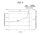
In the crystal growth of GaN by an MOCVD method under a high temperature atmosphere of from 900 to 1,000° C., Mg atoms in the ScAlMgO4 substrate 001 are partially decomposed and evaporated, and are diffused into the GaN crystal 004. For the ScAlMgO4 substrate 001 around the opening 008 of the mask layer 002 (i.e., the region 320 in FIG. 3) and the GaN crystal 004 in the opening 008, the Mg concentration profile in the depth direction is measured by secondary ion mass spectroscopy (SIMS), and the result is shown in FIG. 4. As shown in FIG. 4, the Mg concentration of the GaN crystal 004 in the opening 008 (i.e., the Mg concentration in the region 317 in FIG. 3) is 7×10¹⁷ (atoms/cm3) or more, from which it is understood that the GaN crystal 004 contains Mg. As shown in FIG. 4, furthermore, the Mg concentration increases as approaching the ScAlMgO4 substrate 001, from which it can be said that Mg atoms are diffused from the ScAlMgO4 substrate 001. In the case where the Mg concentration of the GaN crystal 004 in the opening 008 exceeds 5×10²¹ (atoms/cm3), the lattice constant is increased as a result of calculation, but the Mg concentration substituting the Group III element exceeds 10% of the total constitutional atoms of the Group III nitride crystal, and a problem of deterioration in the crystal quality of the Group III nitride semiconductor itself may occur. Therefore, the Mg concentration is preferably from 7×10¹⁷ to 5×10²¹ (atoms/cm3).
The Mg concentration is measured similarly for the GaN crystal 004 that is formed on the protrusion 009 of the mask layer 002 (i.e., the region 318 in FIG. 3). As a result, the GaN crystal 004 does not contain Mg atoms, and substantially no diffusion of Mg atoms is observed.
In the case where the GaN crystal 004 in the region 317 contains Mg atoms in a certain extent (for example, from 7×10¹⁷ to 5×10²¹ (atoms/cm3)), the lattice constant of the GaN crystal 004 formed in the region is increased. As a result, the lattice constant of the GaN crystal 004 becomes closer to the lattice constant of the ScAlMgO4 substrate 001, so as to reduce the stress at the interface between the GaN crystal 004 and the ScAlMgO4 substrate 001, and the inclination of the crystal axis and the warpage are reduced. Consequently, by using an MOCVD method, in which a crystal is grown at a high temperature, as in the embodiment, the GaN crystal 004 having less inclination of the crystal axis and less warpage can be formed on the region 317.
The Mg concentration of the GaN crystal 004 in the opening 008 is more preferably from 1×10²⁰ to 5×10²¹ (atoms/cm3). The factor thereof will be described with reference to the graph illustrated in FIG. 5 showing the dependency of the lattice constant (a-axis lattice constant) on the Mg atom concentration in the case where GaN is doped with Mg. The graph has been obtained herein by calculating the average lattice constant based on the value of the bond length between Ga and Mg in the case where the Ga atom positions in a GaN crystal are replaced by Mg. In the calculation of the bond length between Ga and N, the charge of Ga in the Ga site in the GaN crystal is assumed to be 0 (neutral). The lattice constant in the graph is the lattice constant within the c-plane for the crystal growth, i.e., the (0001) plane, (which is the lattice constant in the direction perpendicular to the c-axis). It is understood from the graph that the lattice constant of GaN is drastically increased when the Mg concentration in the GaN crystal becomes 1×10²⁰ (atoms/cm3) or more. Accordingly, with the Mg concentration of the GaN crystal 004 of from 1×10²⁰ to 5×10²¹ (atoms/cm3), a Group III nitride having good crystal quality can be obtained while decreasing the difference in lattice constant between the seed substrate and the Group III nitride crystal formed thereon.
In the GaN crystal in the region 317, the dislocations (defects 313) formed from the interface to the ScAlMgO4 substrate 001 are concentrated, and the diffusion of Mg atoms is accelerated through the dislocations. According to the mechanism, the GaN crystal 004 in the entire region in contact with the ScAlMgO4 substrate 001 has a larger lattice constant than the other regions. The GaN crystal 004 having such a structure is difficult to suffer warpage even through growing to a larger thickness.
On the other hand, the diffusion of Mg is difficult to occur in the other regions than the region 317 in FIG. 3, such as the region 318 adjacent to the region 317. Accordingly, the Mg content in the regions is substantially zero. This may be also evidenced, for example, by Japanese Journal of Applied Physics, No. 44 (2005), pp. 6495-6504, reporting that the diffusion coefficient with no dislocation is decreased by approximately three orders, as compared to the case with dislocations. Therefore, it can be understood that there is substantially no diffusion of Mg occurring in the GaN crystal 004 adjacent to the region 317 (i.e., the GaN crystal in the regions other than the region 317).
In the case where the GaN crystal 004 having Mg diffused therein is further subjected to crystal growth, the dislocations are converged to suppress the diffusion of Mg atoms gradually. The crystal then becomes closer to the GaN template having a uniform lattice constant. Thus, the Mg concentration of the GaN crystal 004 in the region 317 in FIG. 3 is larger on the side of the ScAlMgO4 substrate, whereas the Mg concentration thereof on the opposite surface is smaller.
Based on the aforementioned mechanism, the production of a Group III nitride semiconductor by the production method of the embodiment enables incorporation of divalent atoms contained in a RAMO4 substrate (which are Mg atoms in the ScAlMgO4 substrate in the embodiment) into a part of a Group III nitride crystal (GaN crystal). The Group III nitride crystal that contains divalent atoms in a part thereof has a lattice constant close to that of the RAMO4 substrate, and has less inclination of the crystal axis and less warpage. Furthermore, by growing a crystal on the Group III nitride crystal that contains divalent atoms in a part thereof as a template, a Group III nitride semiconductor having a Group III nitride crystal having high quality can be obtained.
In the known ammonothermal lateral epitaxial growth, the temperature, at which a GaN crystal is grown, is as low as approximately from 650 to 690° C. Therefore, even though a GaN crystal is grown with an ScAlMgO4 substrate, Mg atoms are substantially not diffused in the GaN crystal 004. The calculation of the diffusion coefficient, for example, by the activation energy of Mg diffusion in GaN described in Solid-State Electronics, vol. 43 (1999), pp. 621-623, shows that the diffusion coefficient of Mg in the growth of GaN by an ammonothermal method is smaller by approximately from 10 to 30 orders than the diffusion coefficient of Mg in the growth of GaN by an MOCVD method. Thus, substantially no diffusion of Mg occurs in the case where a GaN crystal is grown by an ammonothermal method. Therefore, a GaN crystal that is grown by the ammonothermal lateral epitaxial growth contains substantially no Mg.
The dislocation density of the GaN crystal in the region 318 can be 1×10⁶ m−2 by producing the GaN crystal by the aforementioned method, but when a GaN crystal is grown without the mask layer 002 provided, the dislocation density of the GaN crystal (having a thickness of approximately 2 μm) becomes approximately from 3 to 5×107 cm−2. When GaN is epitaxially grown on a sapphire substrate as a seed substrate instead of the ScAlMgO4 substrate, the dislocation density of the GaN crystal thus grown is further increased by approximately 1 to 2 orders.
Dislocations of a GaN crystal are incorporated due to the lattice mismatch and the thermal expansion mismatch of the seed substrate to the GaN crystal (Group III nitride crystal) to be grown. Therefore, it is difficult to avoid dislocations completely when heteroepitaxially grown. A dislocation density of GaN exceeding 1×107 cm−2 may be insufficient in quality of a substrate for a light emitting diode for an illumination and an automobile headlight, and a laser diode. Accordingly, a GaN crystal having a dislocation density of 1×10⁶ m−2 or less is demanded in practical use, and the Group III nitride semiconductor according to the embodiment can satisfy the demand.
MODIFIED EMBODIMENTS
The Group III nitride semiconductor of another embodiment may have an AlxGa1-xN layer 007 (0≦x<1) between the ScAlMgO4 substrate 001 and the GaN crystal 004, a shown in FIG. 2. FIG. 2 is a schematic cross sectional view showing a Group III nitride semiconductor 101 according to a modified embodiment of the aspect.
The AlxGa1-xN layer 007 may be formed, for example, by the following method. Herein, the thickness of the AlxGa1-xN layer 007 is 2 and the content x of Al is 0.02 (2% by atom).
An ScAlMgO4 substrate 001 as a seed substrate is prepared. The substrate thus prepared is subjected to thermal cleaning in a hydrogen atmosphere at approximately 1,000° C., and a buffer layer is then formed to a thickness of approximately from 20 to 50 nm at a low temperature of approximately 600° C. An AlxGa1-xN layer 007 is grown at 1,050° C. by an MOCVD method. A crystal having high quality can be obtained due to the presence of the buffer layer. The composition of the buffer layer is preferably the same as the AlxGa1-xN layer 007.
The content of Al in the AlxGa1-xN layer 007 may be 2% by atom or more and 10% by atom or less since no problem may occur as the lattice constant thereof is not too remote from GaN. After forming the AlxGa1-xN layer 007, the mask layer 002 described in the aforementioned embodiment is formed. While the mask layer 002 in this modified embodiment is formed to have openings 008 in a stripe shape, the shape of the openings 008 of the mask layer 002 is not limited thereto. While the ScAlMgO4 substrate 001 is directly exposed in the openings 008 of the mask layer 002 in the aforementioned embodiment, the AlxGa1-xN layer 007 is exposed in the openings 008 of the mask layer 002 in the modified embodiment. In the modified embodiment, the GaN crystal 004 is grown from the exposed AlxGa1-xN layer 007 as an origin.
In the modified embodiment, defects 313 are also formed in the AlxGa1-xN layer 007 and the GaN crystal 004 that are formed around the opening 008, but the defects are concentrated only in the vicinity of the opening 008 of the mask layer 002, and do not propagate to the majority of the GaN crystal 004. Accordingly, the GaN crystal 004 formed on the protrusion 009 of the mask layer 002 shows high crystallinity.
In the case where a lattice mismatch and a thermal expansion mismatch are largely present between the seed substrate (ScAlMgO4 substrate 001) and the GaN crystal 004 to be grown, the GaN crystal 004 thus grown may be warped due to the residual stress from failure to bond the crystals smoothly in an atomic layer level at a bonding position 316, thereby resulting in further defects in this region in some cases. The further defects may be scattered out to the peripheral portions associated with the further growth of GaN, and may be finally a factor increasing the dislocation density of the entire GaN crystal 004. On the other hand, by providing the AlxGa1-xN layer 007 as in the modified embodiment, the influence of the lattice mismatch and the thermal expansion mismatch can be reduced. Consequently, the region 318 having less defects can be formed on the substantially entire surface except for the region 317 having many defects. The dislocation density in the region 318 having less defects may be less than 1×10⁶ m−2.
In the modified embodiment, the effect of increasing the lattice constants of the AlxGa1-xN layer 007 and the GaN crystal 004 through diffusion of Mg from the ScAlMgO4 substrate 001 thereto is as similar to the aforementioned embodiment. Specifically, Mg atoms are diffused from the ScAlMgO4 substrate 001 to the GaN crystal 004 in the region 319 around the opening 008 of the mask layer 002. As a result, the warpage of the GaN crystal 004 is reduced to provide the GaN crystal 004 having high quality.
Instead of the AlxGa1-xN layer 007, a layer formed of a mixed crystal AlxGayIn1-x-yN (0≦x<1 and x+y=1) having In added thereto may be used.
Others
The Group III nitride semiconductor of the aspect can be applied to various purposes. For example, the Group III nitride semiconductor of the aspect can be applied to a substrate and the like of various light emitting devices. In this case, an AlGaInN crystal, which is a light emitting layer of a light emitting diode having a light emission wavelength in a range of ultraviolet to red, and a laser diode, is grown on the Group III nitride crystal by an MOCVD method or the like. The formation of the light emitting layer by using the Group III nitride semiconductor of the aspect reduces the defect density of the light emitting layer. Consequently, the light emitting device can be remarkably improved in light emission efficiency and operation lifetime.
While the aforementioned embodiments describe the production of the GaN crystal by the MOCVD method, the GaN crystal may be produced, for example, by a hydride vapor phase epitaxy (HVPE) method, an oxide vapor phase epitaxy (OVPE) method, or the like. The temperature of the substrate in the crystal growth is approximately 1,000° C. or more in both the HVPE method and the OVPE method, as similar to the MOCVD method, and the diffusion of Mg atoms from the ScAlMgO4 substrate occurs. An independent substrate of GaN may be produced in such a manner that a GaN layer having a thickness of several hundred micrometers to several millimeters is formed by an HVPE method or an OVPE method on the GaN crystal as the Group III nitride semiconductor produced by the MOCVD method, and then the ScAlMgO4 substrate is removed by such a measure as polishing.
While the aforementioned embodiments describe the examples where a GaN crystal is formed as the Group III nitride crystal, the Group III nitride crystal formed in the embodiments is not limited to a GaN crystal. For example, AlxGa1-xN (0≦x≦1) may be formed at a high temperature of approximately from 900 to 1,000° C. in the similar manner as above. However, the increase of the Al content may decrease the selective growth of the crystal due to AlN polycrystals accumulated on the mask layer 002. Accordingly, the concentration of Al contained in the crystal is preferably more than 0% by atom and 10% by atom or less, and more preferably more than 0% by atom and 5% by atom or less.
After producing a GaN crystal by the aforementioned method, the ScAlMgO4 substrate (RAMO4 substrate) and the dissimilar film are removed to extract the Group III nitride crystal, which may be used as a Group III nitride semiconductor. The ScAlMgO4 substrate (RAMO4 substrate) and the dissimilar film may be removed by grinding, polishing, or the like.
According to the production of a Group III nitride semiconductor by the method of the aspect, a Group III nitride semiconductor is obtained containing a Group III nitride crystal having a region that contains one or a plurality of divalent elements selected from the group consisting of Mg, Mn, Fe(II), Co, Cu, Zn, and Cd, and a region that does not contain the divalent element, in which the regions are distributed alternately within one plane constituting the crystal. The Group III nitride semiconductor contains the region that contains the divalent element, and thus is a Group III nitride semiconductor having high quality that is relieved from the mismatch of the lattice constants of the RAMO4 substrate and the Group III nitride crystal occurring in the production of the Group III nitride crystal. The concentration of the divalent element in the region that contains the divalent element is preferably from 7×10¹⁷ to 5×10²¹ (atoms/cm3), and more preferably from 1×10²⁰ to 5×10²¹ (atoms/cm3). When the divalent element is contained in a concentration within the range, the Group III nitride semiconductor produced may have high quality. As described above, in the case where ScAlMgO4 is used as the substrate for producing the Group III nitride semiconductor, the divalent element is Mg. The Group III nitride crystal in the Group III nitride semiconductor is preferably a GaN crystal.
The Group III nitride semiconductor of the aspect can be applied to a seed substrate for crystal growth of a white LED used for an illumination, an automobile headlight, and the like, and a laser diode.

Claims (17)

What is claimed is:
1. A Group III nitride semiconductor comprising:
a RAMO4 substrate containing a single crystal represented by a general formula RAMO4 (wherein R represents one or a plurality of trivalent elements selected from a group of elements including: Sc, In, Y, and a lanthanoid element, A represents one or a plurality of trivalent elements selected from a group of elements including: Fe(III), Ga, and Al, and M represents one or a plurality of divalent elements selected from a group of elements including: Mg, Mn, Fe(II), Co, Cu, Zn, and Cd);
a dissimilar film that is disposed on the RAMO4 substrate, contains a material different from the RAMO4 substrate, and has plural openings; and
a Group III nitride crystal that is disposed on the dissimilar film and in the openings of the dissimilar film, contains a material different from the dissimilar film, and contains an element represented by M in the general formula.
2. The Group III nitride semiconductor according to claim 1, wherein the Group III nitride crystal has a concentration of the element represented by M in the openings of the dissimilar film of from 7×10¹⁷ to 5×10²¹ (atoms/cm3).
3. The Group III nitride semiconductor according to claim 1, wherein the Group III nitride crystal has a concentration of the element represented by M in the openings of the dissimilar film of from 1×10²⁰ to 5×10²¹ (atoms/cm3).
4. The Group III nitride semiconductor according to claim 1, wherein the dissimilar film is in direct contact with the RAMO4 substrate.
5. The Group III nitride semiconductor according to claim 1, wherein the dissimilar film contains a dielectric material or a metal.
6. The Group III nitride semiconductor according to claim 1, wherein the Group III nitride crystal is in direct contact with the RAMO4 substrate through the plural openings of the dissimilar film.
7. The Group III nitride semiconductor according to claim 1, wherein in the general formula, R is Sc, A is Al, and M is Mg.
8. A Group III nitride semiconductor comprising a Group III nitride crystal having a first region that contains one or a plurality of divalent elements selected from a group of elements including: Mg, Mn, Fe(II), Co, Cu, Zn, and Cd, and a second region that does not contain the divalent element, the first and second regions being distributed alternately within one plane constituting the crystal,
wherein the first region includes threading dislocations more than the second region.
9. The Group III nitride semiconductor according to claim 8, wherein the first region contains a concentration of the divalent element of from 7×10¹⁷ to 5×10²¹ (atoms/cm3).
10. The Group III nitride semiconductor according to claim 8, wherein the first region contains a concentration of the divalent element of from 1×10²⁰ to 5×10²¹ (atoms/cm3).
11. The Group III nitride semiconductor according to claim 1, wherein the Group III nitride crystal is GaN.
12. A method for producing a Group III nitride semiconductor, comprising:
preparing a RAMO4 substrate containing a single crystal represented by a general formula RAMO4 (wherein R represents one or a plurality of trivalent elements selected from a group consisting of Sc, In, Y, and a lanthanoid element, A represents one or a plurality of trivalent elements selected from a group consisting of Fe(III), Ga, and Al, and M represents one or a plurality of divalent elements selected from a group consisting of Mg, Mn, Fe(II), Co, Cu, Zn, and Cd);
forming a dissimilar film that contains a material different from the RAMO4 substrate, and has plural openings, on the RAMO4 substrate; and
forming a Group III nitride crystal that contains a material different from the dissimilar film, on the dissimilar film, at a temperature of from 900 to 1,000° C.
13. The method for producing a Group III nitride semiconductor according to claim 12, wherein the dissimilar film is formed in direct contact with the RAMO4 substrate.
14. The method for producing a Group III nitride semiconductor according to claim 12, wherein the dissimilar film contains a dielectric material or a metal.
15. The method for producing a Group III nitride semiconductor according to claim 12, wherein the Group III nitride crystal is formed in direct contact with the RAMO4 substrate through the plural openings of the dissimilar film.
16. The method for producing a Group III nitride semiconductor according to claim 12, wherein in the general formula, R is Sc, A is Al, and M is Mg.
17. The method for producing a Group III nitride semiconductor according to claim 12, wherein the Group III nitride crystal is GaN.
US15/431,721 2016-03-23 2017-02-13 Group III nitride semiconductor and method for producing same Active US9899564B2 (en)

Applications Claiming Priority (4)

Application Number Priority Date Filing Date Title
JP2016057973 2016-03-23
JP2016-057973 2016-03-23
JP2016-223291 2016-11-16
JP2016223291A JP6249250B2 (en) 2016-03-23 2016-11-16 Group III nitride semiconductor and method of manufacturing the same

Publications (2)

Publication Number Publication Date
US20170279003A1 US20170279003A1 (en) 2017-09-28
US9899564B2 true US9899564B2 (en) 2018-02-20

Family

ID=59898272

Family Applications (1)

Application Number Title Priority Date Filing Date
US15/431,721 Active US9899564B2 (en) 2016-03-23 2017-02-13 Group III nitride semiconductor and method for producing same

Country Status (2)

Country Link
US (1) US9899564B2 (en)
CN (1) CN107227490B (en)

Families Citing this family (5)

* Cited by examiner, † Cited by third party
Publication number Priority date Publication date Assignee Title
EP3618123A4 (en) * 2017-04-24 2020-05-13 Enkris Semiconductor, Inc. SEMICONDUCTOR STRUCTURE AND METHOD FOR MANUFACTURING SEMICONDUCTOR STRUCTURE
US10886435B2 (en) 2017-11-16 2021-01-05 Panasonic Corporation Group III nitride semiconductor with InGaN diffusion blocking layer
CN112334606A (en) * 2018-06-26 2021-02-05 株式会社Flosfia Crystalline oxide film
JP7133786B2 (en) * 2018-10-29 2022-09-09 パナソニックIpマネジメント株式会社 III-nitride semiconductor and manufacturing method thereof
JP7182262B2 (en) * 2018-12-10 2022-12-02 パナソニックIpマネジメント株式会社 RAMO4 SUBSTRATE AND MANUFACTURING METHOD THEREOF, AND GROUP III NITRIDE SEMICONDUCTOR

Citations (25)

* Cited by examiner, † Cited by third party
Publication number Priority date Publication date Assignee Title
JPS4933556A (en) 1972-07-25 1974-03-28
US4177321A (en) 1972-07-25 1979-12-04 Semiconductor Research Foundation Single crystal of semiconductive material on crystal of insulating material
JPS61234547A (en) 1985-04-11 1986-10-18 Aisin Seiki Co Ltd Manufacture of semiconductor substrate
JPH1143398A (en) 1997-07-22 1999-02-16 Mitsubishi Cable Ind Ltd Substrate for growing gallium nitride-based crystal and use thereof
US6656615B2 (en) * 2001-06-06 2003-12-02 Nichia Corporation Bulk monocrystalline gallium nitride
US6693021B1 (en) * 1997-10-30 2004-02-17 Sumitomo Electric Industries, Ltd. GaN single crystal substrate and method of making the same
US6855620B2 (en) * 2000-04-28 2005-02-15 Toyoda Gosei Co., Ltd. Method for fabricating Group III nitride compound semiconductor substrates and semiconductor devices
US6861305B2 (en) * 2000-03-31 2005-03-01 Toyoda Gosei Co., Ltd. Methods for fabricating group III nitride compound semiconductors and group III nitride compound semiconductor devices
US20050208687A1 (en) * 2004-03-17 2005-09-22 Sumitomo Electric Industries, Ltd. Method of Manufacturing Single-Crystal GaN Substrate, and Single-Crystal GaN Substrate
US7141444B2 (en) * 2000-03-14 2006-11-28 Toyoda Gosei Co., Ltd. Production method of III nitride compound semiconductor and III nitride compound semiconductor element
US20080087919A1 (en) * 2006-10-08 2008-04-17 Tysoe Steven A Method for forming nitride crystals
US20080163814A1 (en) * 2006-12-12 2008-07-10 The Regents Of The University Of California CRYSTAL GROWTH OF M-PLANE AND SEMIPOLAR PLANES OF (Al, In, Ga, B)N ON VARIOUS SUBSTRATES
US20090197399A1 (en) 2008-02-01 2009-08-06 Sumitomo Electric Industries, Ltd. Method of growing group iii-v compound semiconductor, and method of manufacturing light-emitting device and electron device
US20110163323A1 (en) * 1997-10-30 2011-07-07 Sumitomo Electric Industires, Ltd. GaN SINGLE CRYSTAL SUBSTRATE AND METHOD OF MAKING THE SAME
US20120199952A1 (en) * 2012-01-09 2012-08-09 Soraa, Inc. Method for Growth of Indium-Containing Nitride Films
US20130075785A1 (en) * 2011-09-28 2013-03-28 Fujitsu Limited Semiconductor device and fabrication method
US20130244364A1 (en) 2010-11-02 2013-09-19 Koninklijke Philips Electronics N.V. Method of forming a composite substrate
JP2013544436A (en) 2010-11-02 2013-12-12 コーニンクレッカ フィリップス エヌ ヴェ Group III nitride light-emitting device
US20140147650A1 (en) * 2012-11-26 2014-05-29 Soraa, Inc. High quality group-iii metal nitride crystals, mehods of making, and methods of use
US20140217553A1 (en) * 2010-11-23 2014-08-07 Arizona Board Of Regents For And On Behalf Of Arizona State University Template layers for heteroepitaxial deposition of iii nitride semiconductor materials using hvpe processes
US20140357053A1 (en) * 2012-03-14 2014-12-04 Sino Nitride Semiconductor Co., LTD Method for Preparing Composite Substrate Used For GaN Growth
JP2015178448A (en) 2014-02-28 2015-10-08 国立大学法人東北大学 Method for manufacturing single crystal substrate and method for manufacturing laser element
US9396941B2 (en) * 2010-09-17 2016-07-19 The United States Of America, As Represented By The Secretary Of The Navy Method for vertical and lateral control of III-N polarity
US20170067182A1 (en) * 2014-04-14 2017-03-09 Sumitomo Chemical Company, Limited Nitride semiconductor single crystal substrate manufacturing method
US20170207307A1 (en) * 2014-01-23 2017-07-20 Intel Corporation Iii-n devices in si trenches

Family Cites Families (3)

* Cited by examiner, † Cited by third party
Publication number Priority date Publication date Assignee Title
JP3920315B2 (en) * 2004-06-14 2007-05-30 三菱電線工業株式会社 Nitride semiconductor light emitting device
CN101484983A (en) * 2006-05-01 2009-07-15 三菱化学株式会社 Etching method, etching mask and method for manufacturing semiconductor device using the same
JP6262561B2 (en) * 2014-02-19 2018-01-17 古河機械金属株式会社 Method for evaluating group III nitride semiconductor substrate

Patent Citations (29)

* Cited by examiner, † Cited by third party
Publication number Priority date Publication date Assignee Title
JPS4933556A (en) 1972-07-25 1974-03-28
US4177321A (en) 1972-07-25 1979-12-04 Semiconductor Research Foundation Single crystal of semiconductive material on crystal of insulating material
JPS61234547A (en) 1985-04-11 1986-10-18 Aisin Seiki Co Ltd Manufacture of semiconductor substrate
JPH1143398A (en) 1997-07-22 1999-02-16 Mitsubishi Cable Ind Ltd Substrate for growing gallium nitride-based crystal and use thereof
US20110163323A1 (en) * 1997-10-30 2011-07-07 Sumitomo Electric Industires, Ltd. GaN SINGLE CRYSTAL SUBSTRATE AND METHOD OF MAKING THE SAME
US6693021B1 (en) * 1997-10-30 2004-02-17 Sumitomo Electric Industries, Ltd. GaN single crystal substrate and method of making the same
US7141444B2 (en) * 2000-03-14 2006-11-28 Toyoda Gosei Co., Ltd. Production method of III nitride compound semiconductor and III nitride compound semiconductor element
US6861305B2 (en) * 2000-03-31 2005-03-01 Toyoda Gosei Co., Ltd. Methods for fabricating group III nitride compound semiconductors and group III nitride compound semiconductor devices
US6855620B2 (en) * 2000-04-28 2005-02-15 Toyoda Gosei Co., Ltd. Method for fabricating Group III nitride compound semiconductor substrates and semiconductor devices
US6656615B2 (en) * 2001-06-06 2003-12-02 Nichia Corporation Bulk monocrystalline gallium nitride
US20050208687A1 (en) * 2004-03-17 2005-09-22 Sumitomo Electric Industries, Ltd. Method of Manufacturing Single-Crystal GaN Substrate, and Single-Crystal GaN Substrate
US20080087919A1 (en) * 2006-10-08 2008-04-17 Tysoe Steven A Method for forming nitride crystals
US20080163814A1 (en) * 2006-12-12 2008-07-10 The Regents Of The University Of California CRYSTAL GROWTH OF M-PLANE AND SEMIPOLAR PLANES OF (Al, In, Ga, B)N ON VARIOUS SUBSTRATES
US20090197399A1 (en) 2008-02-01 2009-08-06 Sumitomo Electric Industries, Ltd. Method of growing group iii-v compound semiconductor, and method of manufacturing light-emitting device and electron device
JP2009184836A (en) 2008-02-01 2009-08-20 Sumitomo Electric Ind Ltd III-V compound semiconductor crystal growth method, light emitting device manufacturing method, and electronic device manufacturing method
US9396941B2 (en) * 2010-09-17 2016-07-19 The United States Of America, As Represented By The Secretary Of The Navy Method for vertical and lateral control of III-N polarity
JP2013542608A (en) 2010-11-02 2013-11-21 コーニンクレッカ フィリップス エヌ ヴェ Method for forming composite substrate
US20130244364A1 (en) 2010-11-02 2013-09-19 Koninklijke Philips Electronics N.V. Method of forming a composite substrate
JP2013544436A (en) 2010-11-02 2013-12-12 コーニンクレッカ フィリップス エヌ ヴェ Group III nitride light-emitting device
US20150115299A1 (en) 2010-11-02 2015-04-30 Koninklijke Philips Electronics N.V. Iii-nitride light emitting device
US20140217553A1 (en) * 2010-11-23 2014-08-07 Arizona Board Of Regents For And On Behalf Of Arizona State University Template layers for heteroepitaxial deposition of iii nitride semiconductor materials using hvpe processes
US20130075785A1 (en) * 2011-09-28 2013-03-28 Fujitsu Limited Semiconductor device and fabrication method
US20120199952A1 (en) * 2012-01-09 2012-08-09 Soraa, Inc. Method for Growth of Indium-Containing Nitride Films
US20140357053A1 (en) * 2012-03-14 2014-12-04 Sino Nitride Semiconductor Co., LTD Method for Preparing Composite Substrate Used For GaN Growth
US20140147650A1 (en) * 2012-11-26 2014-05-29 Soraa, Inc. High quality group-iii metal nitride crystals, mehods of making, and methods of use
JP2014111527A (en) 2012-11-26 2014-06-19 Soraa Inc Iii group metal nitride crystal and method of forming the same
US20170207307A1 (en) * 2014-01-23 2017-07-20 Intel Corporation Iii-n devices in si trenches
JP2015178448A (en) 2014-02-28 2015-10-08 国立大学法人東北大学 Method for manufacturing single crystal substrate and method for manufacturing laser element
US20170067182A1 (en) * 2014-04-14 2017-03-09 Sumitomo Chemical Company, Limited Nitride semiconductor single crystal substrate manufacturing method

Non-Patent Citations (3)

* Cited by examiner, † Cited by third party
Title
Hellman et al., "ScAlMgO4: an oxide Substrate for GaN Epitaxy", Jan. 1996, MRS Internet Journal of Nitride Semiconductor Research, vol. 1, Article 1, 11 pages. *
Kukushkin et al., "Substrates for Epitaxy of Gallium Nitride: New Materials and Techniques," Dec. 2008, Rev. Adv. Mater. Sci. 17 (2008) pp. 1-32. *
Miskys et al., "Freestanding GaN-substrates and devices", Aug. 2003, phys. stat. sol. (c) 0 No. 6, pp. 1627-1650. *

Also Published As

Publication number Publication date
CN107227490B (en) 2021-06-18
US20170279003A1 (en) 2017-09-28
CN107227490A (en) 2017-10-03

Similar Documents

Publication Publication Date Title
US7935615B2 (en) III-V nitride semiconductor substrate and its production method
EP2518191B1 (en) Template for epitaxial growth and process for producing same
CA2747574C (en) Manufacturing of low defect density free-standing gallium nitride substrates and devices fabricated thereof
CN1734247B (en) Group III-V nitride-based semiconductor substrate, manufacturing method thereof, and group III-V nitride-based semiconductor
JP5099763B2 (en) Substrate manufacturing method and group III nitride semiconductor crystal
US8803189B2 (en) III-V compound semiconductor epitaxy using lateral overgrowth
EP2553716B1 (en) Iii-v semiconductor structures and methods for forming the same
US9899564B2 (en) Group III nitride semiconductor and method for producing same
JP4529846B2 (en) III-V nitride semiconductor substrate and method for manufacturing the same
US20110003420A1 (en) Fabrication method of gallium nitride-based compound semiconductor
US9899213B2 (en) Group III nitride semiconductor, and method for producing same
JP4860736B2 (en) Semiconductor structure and method of manufacturing the same
JP6249250B2 (en) Group III nitride semiconductor and method of manufacturing the same
JP2011216549A (en) METHOD OF MANUFACTURING GaN-BASED SEMICONDUCTOR EPITAXIAL SUBSTRATE
JP2007317752A (en) Template substrate
JP2007314360A (en) Template substrate
KR100941596B1 (en) Method for manufacturing group 3-5 compound semiconductor and semiconductor device
JP5073623B2 (en) Method for growing zinc oxide based semiconductor and method for manufacturing semiconductor light emitting device
KR101094409B1 (en) Method for producing gallium nitride single crystal thick film
WO2007078065A1 (en) Gallium nitride-based compound semiconductor
WO2023145799A1 (en) Semiconductor substrate manufacturing method and manufacturing device, and control device
JP2005179089A (en) Epitaxial lateral overgrowth substrate, method of manufacturing the same, and nitride semiconductor device having the epitaxial lateral overgrowth substrate

Legal Events

Date Code Title Description
AS Assignment

Owner name: PANASONIC INTELLECTUAL PROPERTY MANAGEMENT CO., LT

Free format text: ASSIGNMENT OF ASSIGNORS INTEREST;ASSIGNORS:ISHIBASHI, AKIHIKO;UETA, AKIO;SIGNING DATES FROM 20170111 TO 20170112;REEL/FRAME:042071/0386

STCF Information on status: patent grant

Free format text: PATENTED CASE

MAFP Maintenance fee payment

Free format text: PAYMENT OF MAINTENANCE FEE, 4TH YEAR, LARGE ENTITY (ORIGINAL EVENT CODE: M1551); ENTITY STATUS OF PATENT OWNER: LARGE ENTITY

Year of fee payment: 4

MAFP Maintenance fee payment

Free format text: PAYMENT OF MAINTENANCE FEE, 8TH YEAR, LARGE ENTITY (ORIGINAL EVENT CODE: M1552); ENTITY STATUS OF PATENT OWNER: LARGE ENTITY

Year of fee payment: 8