US9892882B1 - Inverted magnetron with amplifying structure and associated systems and methods - Google Patents
Inverted magnetron with amplifying structure and associated systems and methods Download PDFInfo
- Publication number
- US9892882B1 US9892882B1 US15/487,763 US201715487763A US9892882B1 US 9892882 B1 US9892882 B1 US 9892882B1 US 201715487763 A US201715487763 A US 201715487763A US 9892882 B1 US9892882 B1 US 9892882B1
- Authority
- US
- United States
- Prior art keywords
- anode block
- magnetron
- downstream
- excitation ring
- resonant
- Prior art date
- Legal status (The legal status is an assumption and is not a legal conclusion. Google has not performed a legal analysis and makes no representation as to the accuracy of the status listed.)
- Expired - Fee Related
Links
Images


Classifications
-
- H—ELECTRICITY
- H01—ELECTRIC ELEMENTS
- H01J—ELECTRIC DISCHARGE TUBES OR DISCHARGE LAMPS
- H01J23/00—Details of transit-time tubes of the types covered by group H01J25/00
- H01J23/16—Circuit elements, having distributed capacitance and inductance, structurally associated with the tube and interacting with the discharge
- H01J23/24—Slow-wave structures, e.g. delay systems
-
- H—ELECTRICITY
- H01—ELECTRIC ELEMENTS
- H01J—ELECTRIC DISCHARGE TUBES OR DISCHARGE LAMPS
- H01J23/00—Details of transit-time tubes of the types covered by group H01J25/00
- H01J23/36—Coupling devices having distributed capacitance and inductance, structurally associated with the tube, for introducing or removing wave energy
- H01J23/38—Coupling devices having distributed capacitance and inductance, structurally associated with the tube, for introducing or removing wave energy to or from the discharge
-
- H—ELECTRICITY
- H01—ELECTRIC ELEMENTS
- H01J—ELECTRIC DISCHARGE TUBES OR DISCHARGE LAMPS
- H01J23/00—Details of transit-time tubes of the types covered by group H01J25/00
- H01J23/36—Coupling devices having distributed capacitance and inductance, structurally associated with the tube, for introducing or removing wave energy
- H01J23/40—Coupling devices having distributed capacitance and inductance, structurally associated with the tube, for introducing or removing wave energy to or from the interaction circuit
Definitions
- the present invention relates to magnetrons. More specifically, this invention pertains to a compact and efficient magnetron design for delivery of high power microwave (HPM) radiation, and associated systems and methods.
- HPM high power microwave
- HPM generation may only occur if high electromagnetic power (of the order of Gigawatts) is delivered to the device.
- a pulsed power system is typically utilized to deliver this power.
- the electric current emitted is limited by the cathode surface area.
- Magnetron size has also been a limiting factor for HPM system deployment and use.
- Relativistic magnetrons used in traditional HPM systems typically exceed a 10 cm radius, thus presenting a logistical challenge to their deployment on compact mobile platforms.
- the size problem of traditional relativistic magnetrons is compounded when the magnetron's radio frequency (RF) extraction method is considered.
- Standard relativistic magnetrons extract radially through one or more of the resonant cavities of the device. This often results in a network of slots and waveguides that further increase the size and weight of the device.
- RF radio frequency
- a combiner and mode converter are used to combine the RF signal. This additional componentry increases the size and weight of traditional HPM systems.
- inventions of the present invention are related to a compact high power, low voltage, relativistic Inverted Magnetron Oscillator (IMO) for generating electromagnetic waves.
- the IMO may comprise a first end defined as an upstream end, and a second end positioned axially opposite the first end of the magnetron, and defined as a downstream end.
- the IMO may comprise a breech portion at the first end and comprising an upstream opening, a cylindrical passage, an upstream taper, and a reflector chamber in communication with the cylindrical passage. At least a portion of the magnetron may be configured to be operable within a magnetic field.
- the breech portion may be configured to receive pulsed input energy.
- the IMO may further comprise a slow wave structure including an anode block characterized by an anode block first end, an anode block body, an anode block second end, and a plurality of vane panels.
- a slow wave structure including an anode block characterized by an anode block first end, an anode block body, an anode block second end, and a plurality of vane panels.
- Each of the vane panels may be characterized by vane panel tips and each may alternate between positive and negative charges.
- Each of a plurality of resonant cavities defined by the vane panels may comprise a respective resonant channel positioned radially proximate to and axially coextensive with a center axis of the anode block.
- the IMO may further comprise a field emission cathode surrounding the anode block, defining an interaction region therebetween.
- An RF extraction mechanism may comprise a first excitation ring connected to the anode block at alternating vane panels by a first plurality of connecting rods, and, optionally, a second excitation ring connected to the anode block by a second plurality of connecting rods at vane panels not connected to the first plurality of connecting rods.
- the IMO may further comprise a waveguide capacitively coupled to the slow wave structure, and positioned proximate the downstream end of the magnetron.
- the waveguide may be configured to shape electromagnetic waves received from the RF extraction mechanism.
- the first is the slow wave structure which allows the device to operate in the ⁇ mode.
- the second is the excitation ring which, because it is mounted on alternating vanes of the slow wave structure, oscillates from positive to negative (provided the device operates in the ⁇ mode.)
- the third element is the downstream cylindrical waveguide.
- the oscillating ring excites the TM 01 electromagnetic cylindrical mode (as a matter of definition, TM mn refers to a transverse magnetic mode for a circular waveguide where m is the number of full-wave patterns along the circumference of the waveguide and n is the number of half-wave patterns along the diameter of the waveguide).
- the downstream cylindrical carries the TM 01 mode away from the source. If an operator is interested in radiating a TM 01 mode then there is no need for a mode converter. There is no need for combiners in the present invention because all electromagnetic energy is propagated through the waveguide. For the electrons to give up their energy to the electromagnetic wave (mode) and thus create high power electromagnetic energy, the wave and the electron must be allowed to interact in a synchronous way.
- the solution in the present invention is to slow the wave down so that the electron and wave may interact for energy exchange to take place.
- the slow wave structure has the effect of slowing down the ambient electromagnetic wave in the interaction and thus allowing the energy exchange to take place
- the excitation rings of the present invention advantageously operate to extract electromagnetic energy.
- the terms “ring” and “RF extraction mechanism” may be used interchangeably because the ring is the key component for RF extraction. Because the ring is mounted on alternating vanes of the slow wave structure it (the ring) will have uniform polarity. This is because the slow wave structure allows the magnetron to operate in the ⁇ mode. ( ⁇ mode describes a condition where alternating vanes have identical polarity). This polarity will alternate with the alternating polarity of the vanes on which it (the ring) is mounted. The oscillations then excite the TM 01 mode of the cylindrical waveguide.
- the ring advantageously allows electromagnetic energy to leave the device (i.e. for radiation to occur).
- a second ring may be mounted to the remaining vanes on which the first ring is not mounted.
- the second ring will have opposite polarity to the first ring. Because the second ring is approximately half a wavelength downstream of the first, the TM 01 mode that the second ring induces will interfere constructively with the mode generated by the first ring and thus boost the amplitude of the wave.
- FIG. 1 is an assembled, perspective top view of a magnetron according to an embodiment of the present invention.
- FIG. 2 is an assembled, side-sectional view of the magnetron illustrated in FIG. 1 including a first embodiment of an anode block and taken through line 2 - 2 of FIG. 1 .
- FIG. 3 is an assembled, perspective top view of the first embodiment of the anode block illustrated in FIG. 2 .
- FIG. 4 is an assembled, upstream-sectional view of the magnetron illustrated in FIG. 1 taken through line 4 - 4 of FIG. 1 .
- FIG. 5 is an assembled, upstream-sectional view of the magnetron illustrated in FIG. 1 taken through line 5 - 5 of FIG. 1 .
- FIG. 6A is an assembled, exterior upstream view of the magnetron illustrated in FIG. 1 .
- FIG. 6B is an assembled, exterior downstream view of the magnetron illustrated in FIG. 1 .
- FIG. 7 is a graph illustrating ⁇ mode resonance for the magnetron illustrated in FIG. 2 .
- FIG. 8 is a graph illustrating evolution of magnetron modes as simulated for the magnetron illustrated in FIG. 2 .
- FIG. 9 is a schematic diagram illustrating spoking of particles as simulated for the magnetron illustrated in FIG. 2 and taken through line 4 - 4 of FIG. 1 .
- FIG. 10 is a graph illustrating oscillation in ⁇ mode of the magnetron illustrated in FIG. 2 for sampled magnetic fields.
- FIG. 11 is a graph illustrating output power of the magnetron illustrated in FIG. 2 .
- FIG. 12 is a graph illustrating output power efficiency of the magnetron illustrated in FIG. 2 .
- FIG. 13 is an assembled, perspective top view of a second embodiment of an anode block as used with a magnetron according to an embodiment of the present invention.
- FIG. 14 is an assembled, side-sectional view of the magnetron illustrated in FIG. 1 including the second embodiment of the anode block of FIG. 13 and taken through line 2 - 2 of FIGS. 1 and 13 .
- FIG. 15 is an assembled, exterior upstream view of the magnetron illustrated in FIG. 14 .
- FIG. 16 is a graph illustrating evolution of magnetron modes as simulated for the magnetron illustrated in FIG. 14 .
- FIG. 17 is a graph illustrating output power of the magnetron illustrated in FIG. 14 .
- FIG. 18 is a graph illustrating output power efficiency of the magnetron illustrated in FIG. 14 .
- an Inverted Magnetron Oscillator according to an embodiment of the present invention is now described in detail.
- the present invention may be referred to as a IMO system, an IMO device, a magnetron system, an inverted magnetron, a magnetron, a device, a system, a product, and a method.
- IMO Inverted Magnetron Oscillator
- An embodiment of the invention provides a compact high power, low voltage, relativistic Inverted Magnetron Oscillator (IMO).
- IMO relativistic Inverted Magnetron Oscillator
- inverted shall mean that a cathode surrounds an anode block, as opposed to conventional magnetrons that commonly utilize a centrally located cathode with a surrounding anode.
- the present invention overcomes the described problems in the art in that it is a compact, high power, relativistic Inverted Magnetron Oscillator (IMO).
- IMO is capable of supporting ⁇ mode oscillations over a 50 kV wide window absent any significant mode competition at output RF power levels that, in many cases, exceed 500 MW for voltages lower than 360 kV.
- This operation is advantageously achieved with very low axial magnetic field (0.05-0.09 T), with no downstream current loss, and with RF field amplitudes that do not exceed the vacuum breakdown threshold.
- the IMO is compact.
- the IMO has a radius of approximately 10 cm and an axial length of approximately 60 cm and is a relatively small magnetron when considering the operating voltages, magnetic fields, output power and frequency described herein.
- the IMO has a large cathode surface area. Due to the inverted nature of the design, the large cathode surface area advantageously allows for a greater current draw than standard relativistic magnetrons. The larger current means higher output power for lower voltages, making the compact IMO ideal for high power applications and enabling a significant decrease in size and weight of an HPM system that uses the IMO.
- the IMO advantageously operates at magnetic fields that can be at or about a third less than those required for standard relativistic magnetrons, thus featuring greatly reduced power and size demands on the electromagnet or other sources that provides the magnetic field.
- the IMO radiates axially in the TM 01 mode directly into a cylindrical waveguide, multiple waveguides and combiners are not needed.
- Standard relativistic magnetrons radiate radially in multiple waveguides, thus increasing HPM system size and weight. Due to the single-cylinder axial waveguide design described herein, the IMO is not burdened with any of these disadvantages.
- the IMO does not produce any downstream current loss, a consequence faced by standard relativistic magnetrons.
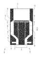
- FIG. 1 illustrates the IMO 100 exterior.
- the IMO 100 may include a first end 101 , referenced herein as an upstream end, and a second end, 102 referenced herein as a downstream end.
- the IMO 100 may include an exterior layer 103 that may extend from the first end 101 to the second end 102 of the IMO 100 .
- the exterior layer 103 may be characterized by a supporting cylinder that may function as a housing to an internal structure and componentry of the IMO 100 .
- the internal structure may be positioned axially inward of the exterior layer 103 and may include an upstream opening 104 , a reflector chamber 105 , an upstream taper 106 , a field emission cathode 107 , an interaction region 108 , a downstream taper 109 , a waveguide 110 , which in the exemplary embodiment is cylindrical, and a downstream opening 111 .
- the upstream opening 104 may be a threshold to a cylindrical passage located substantially proximate the first end 101 of the IMO 100 .
- the internal componentry housed by the exterior layer 103 may include a slow wave structure defined as an anode block 150 .
- the anode block 150 may include an anode block first end 151 , an anode block body 152 , and an anode block second end 153 .
- the anode block body 152 may be positioned coaxial with and surrounded by the field emission cathode 107 .
- the anode block first end 151 and a plurality of vane panel tapers 155 may be positioned substantially proximate to a breech portion 154 of the IMO 100 .
- the breech portion 154 may include the upstream opening 104 positioned adjacent to a cylindrical passage 125 that may extend toward and may connect with the upstream taper 106 .
- the reflector chamber 105 may connect distally with the cylindrical passage 125 .
- Extending distally from the anode block second end 153 may be a first plurality of connecting rods 161 connected to an annular shaped torus, defined as a first excitation ring 162 .
- the anode block body 152 may include a plurality of vane panels 156 , adjacent pairs of which may define resonant cavities 157 therebetween.
- each of the vane panel tapers 155 may be defined by a respective curved portion of the vane panels 156 that may extend from the anode block body 152 down to the anode block first end 151 .
- the slow wave structure/anode block 150 may enable the electrons to give up their energy to the electromagnetic wave (mode) and thus may create high power electromagnetic energy. This happens when the wave and the electron are allowed to interact in a synchronous way. This typically requires the electron and the wave to travel at about the same speed. However, the electrons have mass and thus cannot travel at the speed of light.
- the solution in the present invention is to slow the wave down so that the electron and wave may interact for energy exchange to take place.
- the slow wave structure/anode block 150 may have the effect of advantageously slowing down the ambient electromagnetic wave in the interaction and thus may allow energy exchange to take place.
- the anode block 150 may be characterized by sixteen resonant cavities 157 each defined between a respective pair of radially-projecting vane panels 156 .
- the vane panels 156 may be angled to specifically define the dimensions of the resonant cavities 157 between them.
- Each of the vane panels 156 may comprise a wedge portion 402 that may be adjoined to a respective resonant channel 159 .
- one segment of each vane panel 156 may include vane tips 158 and an opposing segment of each vane panel 156 may be defined by a respective adjacent pair of the resonant channels 159 .
- the resonant channels 159 may be characterized as substantially circular cavities as observed from the IMO 100 first and second ends 101 , 102 , and may be substantially cylindrical cavities 159 as observed from a side-sectional view of the IMO 100 . Therefore, the same voids within the anode block 150 may be described as resonant holes 401 when viewing the anode block first or second end 151 , 153 , but may be described as resonant channels 159 when viewing the anode block 150 from the side.
- Each of the resonant channels 159 may present a respective open portion positioned radially-outward from a center axis of the anode block 150 which may form the segment of each resonant cavity 157 located radially proximate the anode block body 152 .
- the resonant channels 159 may be substantially coaxial and collinear with the center axis of the anode block 150 .
- each of the vane panels 156 may include a wide base 175 located proximate the resonant channels 159 and may include an opposing pair of sides that may angle toward each other to define narrowed vane tips 158 .
- the vane panels 156 may be disposed substantially evenly along an interior perimeter 170 defined by the anode block body 152 , and may project outward from the anode block body 152 with the wider base 175 located proximate the inner perimeter 170 and the narrowed vane tips 158 located distally thereto.
- the resonant cavities 157 produced by the vane panels 156 may be wider between the vane tips 158 and narrower toward the anode block body 152 inner perimeter 170 .
- the field emission cathode 107 may be positioned relative to the anode block 150 so as to define an interaction region 108 of the IMO 100 .
- the field emission cathode 107 may be positioned adjacent to and carried by an interior surface of the exterior layer 103 .
- the cathode 107 may be the origin of charged electron particles that generate HPM radiation. A uniform axial magnetic field may prevent the charged electron particles from immediately accelerating across the interaction region 108 . Instead, the electron particles may undergo rotations about the field emission cathode 107 .
- the electron particles' azimuthal velocity component is approximately equal to the phase velocity of a particular electromagnetic mode in the interaction region 108 , the possibility exists for energy exchange between the particle and the mode.
- This resonance is known as the Buneman-Hartree resonance condition, Benford, J., & Swegle, J. A. (1992). High Power Microwaves , Boston, Ma.: Artech House.
- the electron particles rotate about the field emission cathode 107 they gradually give up their potential energy to a mode or modes of the RF field as they migrate toward the anode block 150 . This interaction may create RF oscillations in the IMO 100 .
- the field emission cathode 107 may measure an outer radius of between 9.9 cm and 10.2 cm and may establish an outer perimeter of the interaction region 108 .
- an outer radius of the field emission cathode 107 may be measured at 10.0 cm.
- An inner boundary of the interaction region 108 may be established by the anode block 150 , which may measure at a radius of 7.1 cm from its center axis to its vane tips 158 .
- the difference between the boundary established by the field emission cathode 107 measuring a radius of 10.0 cm and the boundary established by the anode block 150 measuring a radius of 7.1 cm may create an inter-boundary void surrounding the anode block 150 .
- This inter-boundary void may define the interaction region 108 .
- the axial length of both the field emission cathode 107 and the anode block body 152 (and, therefore, of the interaction region 108 ) may be identical and equal to 26.2526 cm.
- each of the vane panels 156 may present a respective angle that may measure 10.18 degrees with respect to a bisecting plane through an origin of that angle.
- the vane panels 156 may define sixteen resonant cavities 157 therebetween.
- Each of the vane tips 158 may have a width of 0.25 cm.
- Circular voids, defined as resonant holes 401 may exist at the bottom of each resonant cavity 157 when viewing the anode block from the first or second end 151 , 153 and may define the dimensions of the resonant channels 159 that may extend substantially the length of the anode block body 152 .
- the resonant channels 159 are viewable from a side view of the anode block 150 .
- a respective radius of each resonant hole 401 (and therefore resonant channel 159 ) may measure 0.509 cm and a respective center of each resonant hole 401 and resonant channel 159 may be distanced 3.406 cm from the center axis of the anode block 150 .
- the resonant holes 401 and resonant channels 159 may exist to advantageously increase inductance and mode stability of the IMO 100 , as well as to advantageously lower the IMO 100 resonant frequency.
- each of the resonant cavities 157 may subtend a respective angle of 39.5 degrees with respect to the respective resonant holes 401 and resonant channels 159 .
- This measurement may represent the axial coordinate where extraction of RF energy may be accomplished via the first excitation ring 162 , otherwise known as a torus, that may be characterized by a major radius 6.6 cm and minor radius 0.45 cm.
- the first excitation ring 162 may be mounted on a first plurality of connecting rods 161 , each characterized by a radius of 0.2 cm and a length of 1.8 cm.
- the first excitation ring 162 may operate to extract electromagnetic energy.
- the terms “excitation ring” and “RF extraction mechanism” may be used interchangeably because the first excitation ring 162 advantageously operates as a component for RF extraction.
- the excitation ring 162 is mounted on alternating vane panels 156 of the anode block 150 , the first excitation ring 162 may have uniform polarity. This is because the anode block 150 may allow the IMO 100 to operate in the ⁇ mode. ⁇ mode describes a condition where alternating vane panels 156 have identical polarity. This polarity will alternate with the alternating polarity of the vane panels 156 on which the first excitation ring 162 is mounted. The oscillations then excite the TM01 mode of the cylindrical waveguide.
- the cylindrical waveguide 110 may be characterized by a radius of 7.4 cm and may allow for propagation of the TM 01 mode out of the IMO 100 second end 102 and downstream opening 111 .
- the breech portion 154 of the IMO 100 may be located at the IMO first end 101 and may present the upstream opening 104 defined between the exterior layer 103 and the anode block first end 151 .
- the anode block first end 151 conductively coupled to the anode block 150 , may be electrically insulated from the exterior layer 103 , which is conductively connected to the field emission cathode 107 so that the potential difference applied at the upstream end 101 may be transmitted to and may serve as the diode voltage of the magnetron 100 .
- the upstream opening 104 may measure an outer radius of 5 cm before tapering upward to the field emission cathode 107 characterized by a radius of 10.0 cm.
- the upstream taper 106 may be defined by a taper between the upstream opening 104 measuring a radius of 5 cm and the upstream end of the field emission cathode 107 measuring a radius of 10.0 cm.
- the upstream taper 106 may be characterized as a flaring annular passage.
- the upstream taper 106 may represent a curved void within the exterior layer 103 that may surround the vane panel taper 155 of the anode block first end 151 .
- the anode block first end 151 may have a radius measuring 2.84 cm before tapering upward to form the vane panels 156 of the anode block 150 that extend to radii of 7.1 cm to the vane tips 158 .
- the reflector chamber 105 located proximate to the IMO first end 101 and downstream of the breach portion 154 may be a reflector chamber 105 .
- the cylindrically shaped void of the reflector chamber 105 may be positioned perpendicular to the center axis of the anode block 150 and adjacent the upstream opening 104 , thereby combining the reflector chamber 105 and the cylindrical passage 125 defined between the upstream opening 104 and the upstream taper 106 .
- the reflector chamber 105 may advantageously prevent upstream RF energy loss by reflecting this energy back into the interaction region 108 of the IMO 100 .
- downstream taper 109 Located proximate to the anode block second end 153 and to a downstream end of the field emission cathode 107 may be a downstream taper 109 .
- the downstream taper 109 may define a taper in the exterior layer 103 formed by the difference in diameter between the field emission cathode 107 measuring a radius of 10.0 cm and the inner radius of the cylindrical waveguide 110 measuring 7.4 cm.
- the downstream taper 109 may be defined as a frustoconical void.
- FIGS. 7-12 graphically represent simulation data characterizing operation of the embodiment of the IMO 100 illustrated in FIGS. 1, 2, 3, 4, 5, 6A, and 6B .
- ICEPIC Improved Concurrent Electromagnetic Particle-In-Cell code
- PIC particle-in-cell
- the PIC algorithm is used to solve Maxwell's equations and the relativistic Lorentz force law in the time domain on a fixed staggered grid.
- ICEPIC is designed to run on parallel architecture and thus meet the challenge of full 3D simulations of the MWC magnetron.
- the ICEPIC is a proven code that has been used in a number of high power relativistic magnetron studies Lemke, R. W., Genoni, T. C., & Spencer, T. A. (1999). Three-dimensional particle-in-cell simulation study of a relativistic magnetron. Physics of Plasmas, 6(2), 603-613; and Fleming, T., & Mardahi, P. (2009). Performance Improvements in the Relativistic Magnetron: The Effect of DC Field Perturbations. IEEE Transactions on Plasma Science, 37(11), 2128-2138. Also, referenced for prototyping design and identifying loss mechanisms. Spencer, T., Genoni, T., & Lemke, R. (2000).
- a non-interacting fluid model (single particle) of charged particles employing the Buneman-Hartree resonance condition and the Hull Cut-off condition in a smooth bore geometry yields the region in voltage-magnetic space over which the IMO 100 may oscillate in the ⁇ mode. Oscillations in the ⁇ mode typically occur right above the Buneman-Hartree ⁇ mode curve. Consequently, the presented simulations target this region of the voltage-magnetic field parameter space. Referencing the graph in FIG. 7 , a resolution of one grid cell length equals 0.05 cm on a uniform Cartesian grid.
- the simulated interaction region is well resolved at 58 grid cells.
- the grid volume as simulated was 668, 662, and 1758 cells in the x, y, and z directions, respectively, yielding a total of approximately 777 million grid points. Adding to this computational burden are the charged particle dynamics. Simulations produced about 330 million charged macro-particles.
- Simulations of the presented magnitude may only be performed on large high performance computing resources.
- the presented simulations were carried out on a parallel computing platform using 256 Intel Xeon E5-2697 2.7 GHz cores. Each simulation required approximately 2.0 days to reach 200 ns of simulation time at which time saturation was well established.
- a pulsed power device was used to provide the diode voltage (i.e., DC radial electric field) between the field emission cathode 107 and the anode block 150 .
- the circuit and switches that constitute the pulsed power device were not modeled. Rather, a time dependent voltage function was used to emulate the behavior of the pulsed powered source.
- the voltage function was continuous and consisted of two parts. The first part was a 50 ns linear ramp up followed by a second part that was a constant voltage amplitude which lasted for the duration of the simulation. This amplitude was a free parameter that was manipulated in the presented simulations. Input voltages used in the presented simulations ranged from 200-400 kV.
- a uniform axial magnetic field existed for the duration of the presented simulations.
- This field represented the insulating magnetic field that current carrying coils may generate.
- the coils may produce a magnetic field that may be uniform in the interaction region 108 and throughout most of the IMO 100 .
- the IMO 100 was simulated at magnetic fields of 0.05 T, 0.06 T, 0.07 T, 0.08 T, and 0.09 T.
- the dynamics of the IMO 100 presented are representative of all performed simulations. 375 kV was the dial up voltage and the resultant voltage was 353 kV.
- FIG. 8 illustrates the time evolution of the simulated magnetron modes.
- the simulation exhibited a transient period of mode competition primarily due to the 7 ⁇ /8 mode during the ascent of the ⁇ mode. However, by 75 ns, the 7 ⁇ /8 mode tended toward dissipation and the T mode was dominant. After this, time mode competition was confined to amplitudes less than 1 kV for each competing mode with the amplitude of the 7 ⁇ /8 mode quickly decaying. The ⁇ mode remained the dominant mode at a frequency of approximately 2 GHz for the duration of the simulation.
- FIG. 9 displays the spoking pattern of particles in a sample slice of the interaction region 108 slice in the xy-plane of 2 dx thickness, and as simulated at 150 ns.
- Each particle is represented by a dot 901 .
- Eight particle spokes 902 characteristic of the ⁇ mode in a sixteen-vane IMO 100 , are evident.
- RF output power is evaluated via the area integral of the outward Poynting flux. This integral covers the downstream cylindrical waveguide 110 .
- the plane of integration was located downstream of the interaction region 108 and covered the entire surface area whose normal is the z-axis. RF output power at saturation was approximately 560 MW.
- the IMO 100 operated in accordance with the Buneman-Hartree resonance condition. Operation was robust and predictable over the range of magnetic fields and voltages sampled.
- the voltage window for ⁇ mode oscillation for a given magnetic field was approximately 50 kV which advantageously may provide for advanced performance stability.
- FIG. 12 plots the efficiency of the IMO 100 .
- operation of the IMO 100 exhibited a general increase in RF efficiency as the magnetic field was increased.
- peak efficiency did not correspond with the voltage that produced peak output power.
- the IMO 100 presented in the first embodiment consistently oscillates in the ⁇ mode across a wide range of magnetic fields and voltages.
- the IMO 100 operated in a predictable fashion obeying the Buneman-Hartree resonance condition.
- the ⁇ mode resonance curve was used to successfully predict where the magnetron would oscillate in voltage/magnetic field space (i.e., oscillations tracked well with the curve). Therefore, this embodiment of the present invention advantageously proved stable and reliable.
- FIG. 13 illustrates a second embodiment of the inverted magnetron, defined as IMO-B 1300 .
- IMO-B 1300 may have the same dimensions and specifications as the IMO 100 , but with an added annular shaped torus, defined as a second excitation ring 1302 and a second plurality of connecting rods 1303 extending from the anode block second end 153 .
- the second plurality of connecting rods 1303 may be eight (8) in number.
- the second excitation ring 1302 may be mounted to the remaining vane panels 156 of the anode block 150 via the second plurality of connecting rods 1303 that do not include the first plurality of connecting rods 161 and the mounted first excitation ring 162 .
- the second excitation ring 162 will have opposite polarity to the first excitation ring 162 . Because the second excitation ring 1302 is approximately half a wavelength downstream of the first excitation ring 162 , the TM 01 mode that the second excitation ring 1302 induces may interfere constructively with the mode generated by the first excitation ring 162 and thus boost the amplitude of the wave.
- the second excitation ring 1302 may be positioned 7.56 cm away from the anode block second end 153 .
- the second excitation ring 1302 may measure a major radius of 1.99 cm and a minor radius of 0.45 cm.
- the second excitation ring 1302 may be smaller in diameter than the first excitation ring 162 and may extend distally from the anode block second end 153 by the distance of the second plurality of connecting rods 1303 .
- the distance of the second plurality of connecting rods 1303 may be greater than the distance of the first plurality of connecting rods 161 .
- the second plurality of connecting rods 1303 may be connected to alternating vane panels 156 , proximate the inner perimeter 170 of the anode block second end 153 relative to the first plurality of connecting rods 161 .
- the second plurality of connecting rods 1303 may be located on vane panels 156 not inclusive of the first plurality of connecting rods 161 . Therefore, the first plurality of connecting rods 161 and the second plurality of connecting rods 1303 may be alternated, respectively.
- the second plurality of connecting rods 1303 may be located at the base 175 of the vane panels 156 on the anode block second end 153 before the vane panels 156 become defined by the resonant holes 401 and resonant channels 159 .
- the second plurality of connecting rods 1303 may form an angle other than 90 degrees with the anode block second end 153 to accommodate the smaller diameter of the second excitation ring 1302 relative to the positioning of the second plurality of connecting rods 1303 on the anode block second end 153 .
- FIG. 14 is a side-sectional view of the IMO-B 1300 that illustrates the second plurality of connecting rods 1303 measuring longer than the first plurality of connecting rods 161 and forming an angle between the anode block second end 153 and the second excitation ring 1302 .
- the second plurality of connecting rods 1303 may connect to the anode block second end 153 at one portion, may pass through an inner perimeter established by the first excitation ring 162 , and may connect to the second excitation ring 1302 at a positioning distal to the anode block second end 153 relative to the first excitation ring 162 .
- addition of the second excitation ring may increase the RF output power of the IMO-B 1300 as compared to the IMO 100 .
- the following three fields were used to test the IMO-B 1300 : 0.06 T, 0.065 T and 0.07 T.
- the 305 kV was the dial up voltage and the resultant voltage was 307 kV.
- FIG. 16 plots the mode dynamics of the IMO-B 1300 as a function of time.
- FIG. 17 shows IMO-B 1300 RF Output power performance across a range of voltages.
- RF output power at saturation was approximately 496 MW.
- Output power efficiency was 17.8% with an input current of 9 kA and a measured voltage of 307 kV.
- the IMO so configured exhibited no downstream leakage current.
- peak electric field amplitudes remained well below the Kilpatrick limit for RF breakdown.
- the IMO-B 1300 proved to be advantageously stable and reliable over the voltage and magnetic fields sampled.
- FIG. 18 shows that efficiencies for the IMO-B 1300 behave in a similar manner as the IMO, although average efficiency is slightly less.
Landscapes
- Microwave Tubes (AREA)
Abstract
Description
R o=0.05e (6.9348(z−z
where Ro is the outer radius, zo is the coordinate for the starting point for the
R i=0.0284e (9.16(z−z
where Ri represents the inner radius of the
Claims (20)
Priority Applications (1)
| Application Number | Priority Date | Filing Date | Title |
|---|---|---|---|
| US15/487,763 US9892882B1 (en) | 2017-04-14 | 2017-04-14 | Inverted magnetron with amplifying structure and associated systems and methods |
Applications Claiming Priority (1)
| Application Number | Priority Date | Filing Date | Title |
|---|---|---|---|
| US15/487,763 US9892882B1 (en) | 2017-04-14 | 2017-04-14 | Inverted magnetron with amplifying structure and associated systems and methods |
Publications (1)
| Publication Number | Publication Date |
|---|---|
| US9892882B1 true US9892882B1 (en) | 2018-02-13 |
Family
ID=61148037
Family Applications (1)
| Application Number | Title | Priority Date | Filing Date |
|---|---|---|---|
| US15/487,763 Expired - Fee Related US9892882B1 (en) | 2017-04-14 | 2017-04-14 | Inverted magnetron with amplifying structure and associated systems and methods |
Country Status (1)
| Country | Link |
|---|---|
| US (1) | US9892882B1 (en) |
Cited By (5)
| Publication number | Priority date | Publication date | Assignee | Title |
|---|---|---|---|---|
| CN111128645A (en) * | 2020-01-08 | 2020-05-08 | 深圳市思博克科技有限公司 | X-waveband high-power microwave device for forced stop of vehicles and ships |
| CN111933501A (en) * | 2020-07-22 | 2020-11-13 | 电子科技大学 | Virtual cathode inverted relativistic magnetron |
| CN113488363A (en) * | 2021-07-06 | 2021-10-08 | 电子科技大学 | TE (time-out) device11Relativistic magnetron with mode output |
| CN114783848A (en) * | 2022-03-10 | 2022-07-22 | 电子科技大学 | Axial Cascade Relativistic Magnetron Based on Frequency-locking and Phase-locking of Ridge-Circular Waveguide Coupling Structure |
| CN118888411A (en) * | 2024-06-20 | 2024-11-01 | 电子科技大学 | A compact relativistic magnetron based on a ring-rod extraction structure |
Citations (7)
| Publication number | Priority date | Publication date | Assignee | Title |
|---|---|---|---|---|
| US4041350A (en) * | 1974-11-14 | 1977-08-09 | Tokyo Shibaura Electric Co., Ltd. | Magnetron anode and a method for manufacturing the same |
| US4169987A (en) * | 1977-02-04 | 1979-10-02 | Hitachi, Ltd. | Magnetron tubes cathode support |
| US5635797A (en) * | 1994-03-09 | 1997-06-03 | Hitachi, Ltd. | Magnetron with improved mode separation |
| US20020043937A1 (en) * | 2000-10-18 | 2002-04-18 | Toshio Ogura | Magnetron having a lowered oscillation frequency and processing equipment employing the same |
| US20040140207A1 (en) * | 2003-01-16 | 2004-07-22 | Lg Electronics Inc. | Anode and magnetron therewith |
| US20100052501A1 (en) * | 2007-10-31 | 2010-03-04 | Toshiba Hokuto Electronics Corporation | Brazing material, electron tubes, magnetron and method for brazing |
| US20140191657A1 (en) * | 2013-01-07 | 2014-07-10 | New Japan Radio Co., Ltd. | Coaxial magnetron |
-
2017
- 2017-04-14 US US15/487,763 patent/US9892882B1/en not_active Expired - Fee Related
Patent Citations (7)
| Publication number | Priority date | Publication date | Assignee | Title |
|---|---|---|---|---|
| US4041350A (en) * | 1974-11-14 | 1977-08-09 | Tokyo Shibaura Electric Co., Ltd. | Magnetron anode and a method for manufacturing the same |
| US4169987A (en) * | 1977-02-04 | 1979-10-02 | Hitachi, Ltd. | Magnetron tubes cathode support |
| US5635797A (en) * | 1994-03-09 | 1997-06-03 | Hitachi, Ltd. | Magnetron with improved mode separation |
| US20020043937A1 (en) * | 2000-10-18 | 2002-04-18 | Toshio Ogura | Magnetron having a lowered oscillation frequency and processing equipment employing the same |
| US20040140207A1 (en) * | 2003-01-16 | 2004-07-22 | Lg Electronics Inc. | Anode and magnetron therewith |
| US20100052501A1 (en) * | 2007-10-31 | 2010-03-04 | Toshiba Hokuto Electronics Corporation | Brazing material, electron tubes, magnetron and method for brazing |
| US20140191657A1 (en) * | 2013-01-07 | 2014-07-10 | New Japan Radio Co., Ltd. | Coaxial magnetron |
Cited By (8)
| Publication number | Priority date | Publication date | Assignee | Title |
|---|---|---|---|---|
| CN111128645A (en) * | 2020-01-08 | 2020-05-08 | 深圳市思博克科技有限公司 | X-waveband high-power microwave device for forced stop of vehicles and ships |
| CN111933501A (en) * | 2020-07-22 | 2020-11-13 | 电子科技大学 | Virtual cathode inverted relativistic magnetron |
| CN111933501B (en) * | 2020-07-22 | 2021-09-24 | 电子科技大学 | A Virtual Cathode Inverted Relativistic Magnetron |
| CN113488363A (en) * | 2021-07-06 | 2021-10-08 | 电子科技大学 | TE (time-out) device11Relativistic magnetron with mode output |
| CN113488363B (en) * | 2021-07-06 | 2022-05-03 | 电子科技大学 | A Relativistic Magnetron with TE11 Mode Output |
| CN114783848A (en) * | 2022-03-10 | 2022-07-22 | 电子科技大学 | Axial Cascade Relativistic Magnetron Based on Frequency-locking and Phase-locking of Ridge-Circular Waveguide Coupling Structure |
| CN114783848B (en) * | 2022-03-10 | 2023-06-02 | 电子科技大学 | Axial cascade relativistic magnetron based on ridge waveguide coupling structure frequency locking and phase locking |
| CN118888411A (en) * | 2024-06-20 | 2024-11-01 | 电子科技大学 | A compact relativistic magnetron based on a ring-rod extraction structure |
Similar Documents
| Publication | Publication Date | Title |
|---|---|---|
| US9892882B1 (en) | Inverted magnetron with amplifying structure and associated systems and methods | |
| US8018159B2 (en) | Magnetron device with mode converter and related methods | |
| Zhang et al. | Recent advance in long-pulse HPM sources with repetitive operation in S-, C-, and X-bands | |
| Thumm | Progress on gyrotrons for ITER and future thermonuclear fusion reactors | |
| US8878433B1 (en) | High efficiency, low voltage, low L-band, mega-watt class magnetron | |
| Liu et al. | Investigation of an ${X} $-Band Long Pulse High-Power High-Gain Coaxial Multibeam Relativistic Klystron Amplifier | |
| US20070296515A1 (en) | Magnetron | |
| Lemke et al. | Effects that limit efficiency in relativistic magnetrons | |
| CN115064429B (en) | Coaxial relativistic klystron oscillator with two-stage modulation | |
| Franzi et al. | Recirculating-planar-magnetron simulations and experiment | |
| Vintizenko | Relativistic Magnetrons | |
| McConville et al. | Demonstration of auroral radio emission mechanisms by laboratory experiment | |
| Shen et al. | Research and development of S-band high power multibeam klystron | |
| Mahto et al. | Design and simulation study of the HPM oscillator—Reltron | |
| Krasik et al. | A relativistic magnetron operated with permanent magnets | |
| Singh et al. | Axially partitioned dual band magnetically insulated line oscillator | |
| Gilgenbach et al. | Recirculating planar magnetrons for high-power high-frequency radiation generation | |
| US10192709B2 (en) | Relativistic magnetron using a virtual cathode | |
| Dixit et al. | Study on load-side optimization in bifrequency MILO source | |
| White et al. | Radio frequency priming of a long-pulse relativistic magnetron | |
| Fliflet et al. | Initial operation of a higher-power quasi-optical gyrotron | |
| Cheng et al. | A compact and lightweight relativistic magnetron with permanent magnets | |
| Xu et al. | Design of a high-harmonic gyrotron with a permanent magnet system | |
| Kreischer et al. | High-power operation of a 170 GHz megawatt gyrotron | |
| RU2396632C1 (en) | Klystron generator |
Legal Events
| Date | Code | Title | Description |
|---|---|---|---|
| AS | Assignment |
Owner name: THE GOVERNMENT OF THE UNITED STATES OF AMERICA AS Free format text: ASSIGNMENT OF ASSIGNORS INTEREST;ASSIGNOR:FLEMING, TIMOTHY PAUL;REEL/FRAME:042011/0798 Effective date: 20170315 Owner name: THE GOVERNMENT OF THE UNITED STATES OF AMERICA AS Free format text: ASSIGNMENT OF ASSIGNORS INTEREST;ASSIGNOR:KEISLING, JOHN;REEL/FRAME:042012/0505 Effective date: 20170321 Owner name: THE GOVERNMENT OF THE UNITED STATES OF AMERICA AS Free format text: ASSIGNMENT OF ASSIGNORS INTEREST;ASSIGNOR:MARDAHL, PETER JEROME;REEL/FRAME:042012/0400 Effective date: 20170315 Owner name: THE GOVERNMENT OF THE UNITED STATES OF AMERICA AS Free format text: ASSIGNMENT OF ASSIGNORS INTEREST;ASSIGNOR:LAMBRECHT, MICHAEL RAYMOND;REEL/FRAME:042258/0845 Effective date: 20170315 |
|
| STCF | Information on status: patent grant |
Free format text: PATENTED CASE |
|
| FEPP | Fee payment procedure |
Free format text: MAINTENANCE FEE REMINDER MAILED (ORIGINAL EVENT CODE: REM.); ENTITY STATUS OF PATENT OWNER: LARGE ENTITY |
|
| FEPP | Fee payment procedure |
Free format text: SURCHARGE FOR LATE PAYMENT, LARGE ENTITY (ORIGINAL EVENT CODE: M1554); ENTITY STATUS OF PATENT OWNER: LARGE ENTITY |
|
| MAFP | Maintenance fee payment |
Free format text: PAYMENT OF MAINTENANCE FEE, 4TH YEAR, LARGE ENTITY (ORIGINAL EVENT CODE: M1551); ENTITY STATUS OF PATENT OWNER: LARGE ENTITY Year of fee payment: 4 |
|
| FEPP | Fee payment procedure |
Free format text: MAINTENANCE FEE REMINDER MAILED (ORIGINAL EVENT CODE: REM.); ENTITY STATUS OF PATENT OWNER: LARGE ENTITY |
|
| LAPS | Lapse for failure to pay maintenance fees |
Free format text: PATENT EXPIRED FOR FAILURE TO PAY MAINTENANCE FEES (ORIGINAL EVENT CODE: EXP.); ENTITY STATUS OF PATENT OWNER: LARGE ENTITY |
|
| STCH | Information on status: patent discontinuation |
Free format text: PATENT EXPIRED DUE TO NONPAYMENT OF MAINTENANCE FEES UNDER 37 CFR 1.362 |
|
| FP | Lapsed due to failure to pay maintenance fee |
Effective date: 20260213 |