US9876126B2 - Semiconductor device and semiconductor device manufacturing method - Google Patents
Semiconductor device and semiconductor device manufacturing method Download PDFInfo
- Publication number
- US9876126B2 US9876126B2 US15/296,339 US201615296339A US9876126B2 US 9876126 B2 US9876126 B2 US 9876126B2 US 201615296339 A US201615296339 A US 201615296339A US 9876126 B2 US9876126 B2 US 9876126B2
- Authority
- US
- United States
- Prior art keywords
- refractive index
- waves
- index layers
- semiconductor device
- pair
- Prior art date
- Legal status (The legal status is an assumption and is not a legal conclusion. Google has not performed a legal analysis and makes no representation as to the accuracy of the status listed.)
- Active
Links
- 239000004065 semiconductor Substances 0.000 title claims abstract description 96
- 238000004519 manufacturing process Methods 0.000 title claims description 16
- 238000002834 transmittance Methods 0.000 claims abstract description 37
- 239000012212 insulator Substances 0.000 claims description 27
- 238000000034 method Methods 0.000 claims description 27
- 229910052581 Si3N4 Inorganic materials 0.000 claims description 22
- VYPSYNLAJGMNEJ-UHFFFAOYSA-N Silicium dioxide Chemical compound O=[Si]=O VYPSYNLAJGMNEJ-UHFFFAOYSA-N 0.000 claims description 20
- HQVNEWCFYHHQES-UHFFFAOYSA-N silicon nitride Chemical compound N12[Si]34N5[Si]62N3[Si]51N64 HQVNEWCFYHHQES-UHFFFAOYSA-N 0.000 claims description 18
- 238000004364 calculation method Methods 0.000 claims description 6
- 229910052814 silicon oxide Inorganic materials 0.000 claims description 3
- 239000010410 layer Substances 0.000 description 242
- MKGHDZIEKZPBCZ-ULQPCXBYSA-N methyl (2s,3s,4r,5r,6r)-4,5,6-trihydroxy-3-methoxyoxane-2-carboxylate Chemical compound CO[C@H]1[C@H](O)[C@@H](O)[C@H](O)O[C@@H]1C(=O)OC MKGHDZIEKZPBCZ-ULQPCXBYSA-N 0.000 description 17
- 230000035945 sensitivity Effects 0.000 description 14
- 238000004088 simulation Methods 0.000 description 10
- 239000000463 material Substances 0.000 description 9
- NRTOMJZYCJJWKI-UHFFFAOYSA-N Titanium nitride Chemical compound [Ti]#N NRTOMJZYCJJWKI-UHFFFAOYSA-N 0.000 description 7
- 239000012535 impurity Substances 0.000 description 7
- 230000003595 spectral effect Effects 0.000 description 6
- XUIMIQQOPSSXEZ-UHFFFAOYSA-N Silicon Chemical compound [Si] XUIMIQQOPSSXEZ-UHFFFAOYSA-N 0.000 description 5
- 239000011229 interlayer Substances 0.000 description 5
- 238000000059 patterning Methods 0.000 description 5
- 229910052710 silicon Inorganic materials 0.000 description 5
- 239000010703 silicon Substances 0.000 description 5
- 239000002356 single layer Substances 0.000 description 5
- QGZKDVFQNNGYKY-UHFFFAOYSA-N Ammonia Chemical compound N QGZKDVFQNNGYKY-UHFFFAOYSA-N 0.000 description 4
- BLRPTPMANUNPDV-UHFFFAOYSA-N Silane Chemical compound [SiH4] BLRPTPMANUNPDV-UHFFFAOYSA-N 0.000 description 4
- 235000012239 silicon dioxide Nutrition 0.000 description 4
- 239000000377 silicon dioxide Substances 0.000 description 4
- 239000000758 substrate Substances 0.000 description 4
- 238000001914 filtration Methods 0.000 description 3
- 238000005468 ion implantation Methods 0.000 description 3
- 238000005268 plasma chemical vapour deposition Methods 0.000 description 3
- 230000005855 radiation Effects 0.000 description 3
- 230000035882 stress Effects 0.000 description 3
- CBENFWSGALASAD-UHFFFAOYSA-N Ozone Chemical compound [O-][O+]=O CBENFWSGALASAD-UHFFFAOYSA-N 0.000 description 2
- BOTDANWDWHJENH-UHFFFAOYSA-N Tetraethyl orthosilicate Chemical compound CCO[Si](OCC)(OCC)OCC BOTDANWDWHJENH-UHFFFAOYSA-N 0.000 description 2
- 230000002238 attenuated effect Effects 0.000 description 2
- 230000005540 biological transmission Effects 0.000 description 2
- 230000015572 biosynthetic process Effects 0.000 description 2
- 238000010586 diagram Methods 0.000 description 2
- 238000001312 dry etching Methods 0.000 description 2
- 230000000694 effects Effects 0.000 description 2
- 239000007789 gas Substances 0.000 description 2
- 230000003116 impacting effect Effects 0.000 description 2
- 238000005259 measurement Methods 0.000 description 2
- 229910000069 nitrogen hydride Inorganic materials 0.000 description 2
- 230000003287 optical effect Effects 0.000 description 2
- ZOXJGFHDIHLPTG-UHFFFAOYSA-N Boron Chemical compound [B] ZOXJGFHDIHLPTG-UHFFFAOYSA-N 0.000 description 1
- 201000004624 Dermatitis Diseases 0.000 description 1
- OAICVXFJPJFONN-UHFFFAOYSA-N Phosphorus Chemical compound [P] OAICVXFJPJFONN-UHFFFAOYSA-N 0.000 description 1
- 208000000453 Skin Neoplasms Diseases 0.000 description 1
- 238000001720 action spectrum Methods 0.000 description 1
- 229910021529 ammonia Inorganic materials 0.000 description 1
- 229910052785 arsenic Inorganic materials 0.000 description 1
- RQNWIZPPADIBDY-UHFFFAOYSA-N arsenic atom Chemical compound [As] RQNWIZPPADIBDY-UHFFFAOYSA-N 0.000 description 1
- QVGXLLKOCUKJST-UHFFFAOYSA-N atomic oxygen Chemical compound [O] QVGXLLKOCUKJST-UHFFFAOYSA-N 0.000 description 1
- 229910052796 boron Inorganic materials 0.000 description 1
- 230000006378 damage Effects 0.000 description 1
- 230000003247 decreasing effect Effects 0.000 description 1
- 238000009795 derivation Methods 0.000 description 1
- 210000004207 dermis Anatomy 0.000 description 1
- 238000005530 etching Methods 0.000 description 1
- 230000002070 germicidal effect Effects 0.000 description 1
- 229910021478 group 5 element Inorganic materials 0.000 description 1
- 229910000449 hafnium oxide Inorganic materials 0.000 description 1
- WIHZLLGSGQNAGK-UHFFFAOYSA-N hafnium(4+);oxygen(2-) Chemical compound [O-2].[O-2].[Hf+4] WIHZLLGSGQNAGK-UHFFFAOYSA-N 0.000 description 1
- CJNBYAVZURUTKZ-UHFFFAOYSA-N hafnium(IV) oxide Inorganic materials O=[Hf]=O CJNBYAVZURUTKZ-UHFFFAOYSA-N 0.000 description 1
- 238000005286 illumination Methods 0.000 description 1
- 238000002955 isolation Methods 0.000 description 1
- 230000003647 oxidation Effects 0.000 description 1
- 238000007254 oxidation reaction Methods 0.000 description 1
- 229910052760 oxygen Inorganic materials 0.000 description 1
- 239000001301 oxygen Substances 0.000 description 1
- 229910052698 phosphorus Inorganic materials 0.000 description 1
- 239000011574 phosphorus Substances 0.000 description 1
- 238000005498 polishing Methods 0.000 description 1
- 238000007789 sealing Methods 0.000 description 1
- 238000000926 separation method Methods 0.000 description 1
- 229910000077 silane Inorganic materials 0.000 description 1
- 210000003491 skin Anatomy 0.000 description 1
- 230000009759 skin aging Effects 0.000 description 1
- 201000000849 skin cancer Diseases 0.000 description 1
- 238000004544 sputter deposition Methods 0.000 description 1
- 239000000126 substance Substances 0.000 description 1
Images


Classifications
-
- H—ELECTRICITY
- H01—ELECTRIC ELEMENTS
- H01L—SEMICONDUCTOR DEVICES NOT COVERED BY CLASS H10
- H01L31/00—Semiconductor devices sensitive to infrared radiation, light, electromagnetic radiation of shorter wavelength or corpuscular radiation and specially adapted either for the conversion of the energy of such radiation into electrical energy or for the control of electrical energy by such radiation; Processes or apparatus specially adapted for the manufacture or treatment thereof or of parts thereof; Details thereof
- H01L31/02—Details
- H01L31/0232—Optical elements or arrangements associated with the device
- H01L31/02327—Optical elements or arrangements associated with the device the optical elements being integrated or being directly associated to the device, e.g. back reflectors
-
- H—ELECTRICITY
- H01—ELECTRIC ELEMENTS
- H01L—SEMICONDUCTOR DEVICES NOT COVERED BY CLASS H10
- H01L31/00—Semiconductor devices sensitive to infrared radiation, light, electromagnetic radiation of shorter wavelength or corpuscular radiation and specially adapted either for the conversion of the energy of such radiation into electrical energy or for the control of electrical energy by such radiation; Processes or apparatus specially adapted for the manufacture or treatment thereof or of parts thereof; Details thereof
- H01L31/02—Details
- H01L31/0216—Coatings
- H01L31/02161—Coatings for devices characterised by at least one potential jump barrier or surface barrier
- H01L31/02162—Coatings for devices characterised by at least one potential jump barrier or surface barrier for filtering or shielding light, e.g. multicolour filters for photodetectors
- H01L31/02165—Coatings for devices characterised by at least one potential jump barrier or surface barrier for filtering or shielding light, e.g. multicolour filters for photodetectors using interference filters, e.g. multilayer dielectric filters
-
- G—PHYSICS
- G02—OPTICS
- G02B—OPTICAL ELEMENTS, SYSTEMS OR APPARATUS
- G02B5/00—Optical elements other than lenses
- G02B5/20—Filters
- G02B5/28—Interference filters
- G02B5/283—Interference filters designed for the ultraviolet
-
- H—ELECTRICITY
- H01—ELECTRIC ELEMENTS
- H01L—SEMICONDUCTOR DEVICES NOT COVERED BY CLASS H10
- H01L31/00—Semiconductor devices sensitive to infrared radiation, light, electromagnetic radiation of shorter wavelength or corpuscular radiation and specially adapted either for the conversion of the energy of such radiation into electrical energy or for the control of electrical energy by such radiation; Processes or apparatus specially adapted for the manufacture or treatment thereof or of parts thereof; Details thereof
- H01L31/02—Details
- H01L31/02016—Circuit arrangements of general character for the devices
- H01L31/02019—Circuit arrangements of general character for the devices for devices characterised by at least one potential jump barrier or surface barrier
-
- H—ELECTRICITY
- H01—ELECTRIC ELEMENTS
- H01L—SEMICONDUCTOR DEVICES NOT COVERED BY CLASS H10
- H01L31/00—Semiconductor devices sensitive to infrared radiation, light, electromagnetic radiation of shorter wavelength or corpuscular radiation and specially adapted either for the conversion of the energy of such radiation into electrical energy or for the control of electrical energy by such radiation; Processes or apparatus specially adapted for the manufacture or treatment thereof or of parts thereof; Details thereof
- H01L31/02—Details
- H01L31/0216—Coatings
- H01L31/02161—Coatings for devices characterised by at least one potential jump barrier or surface barrier
- H01L31/02162—Coatings for devices characterised by at least one potential jump barrier or surface barrier for filtering or shielding light, e.g. multicolour filters for photodetectors
- H01L31/02164—Coatings for devices characterised by at least one potential jump barrier or surface barrier for filtering or shielding light, e.g. multicolour filters for photodetectors for shielding light, e.g. light blocking layers, cold shields for infrared detectors
-
- H—ELECTRICITY
- H01—ELECTRIC ELEMENTS
- H01L—SEMICONDUCTOR DEVICES NOT COVERED BY CLASS H10
- H01L31/00—Semiconductor devices sensitive to infrared radiation, light, electromagnetic radiation of shorter wavelength or corpuscular radiation and specially adapted either for the conversion of the energy of such radiation into electrical energy or for the control of electrical energy by such radiation; Processes or apparatus specially adapted for the manufacture or treatment thereof or of parts thereof; Details thereof
- H01L31/08—Semiconductor devices sensitive to infrared radiation, light, electromagnetic radiation of shorter wavelength or corpuscular radiation and specially adapted either for the conversion of the energy of such radiation into electrical energy or for the control of electrical energy by such radiation; Processes or apparatus specially adapted for the manufacture or treatment thereof or of parts thereof; Details thereof in which radiation controls flow of current through the device, e.g. photoresistors
- H01L31/10—Semiconductor devices sensitive to infrared radiation, light, electromagnetic radiation of shorter wavelength or corpuscular radiation and specially adapted either for the conversion of the energy of such radiation into electrical energy or for the control of electrical energy by such radiation; Processes or apparatus specially adapted for the manufacture or treatment thereof or of parts thereof; Details thereof in which radiation controls flow of current through the device, e.g. photoresistors characterised by at least one potential-jump barrier or surface barrier, e.g. phototransistors
- H01L31/101—Devices sensitive to infrared, visible or ultraviolet radiation
- H01L31/1013—Devices sensitive to infrared, visible or ultraviolet radiation devices sensitive to two or more wavelengths, e.g. multi-spectrum radiation detection devices
-
- H—ELECTRICITY
- H01—ELECTRIC ELEMENTS
- H01L—SEMICONDUCTOR DEVICES NOT COVERED BY CLASS H10
- H01L31/00—Semiconductor devices sensitive to infrared radiation, light, electromagnetic radiation of shorter wavelength or corpuscular radiation and specially adapted either for the conversion of the energy of such radiation into electrical energy or for the control of electrical energy by such radiation; Processes or apparatus specially adapted for the manufacture or treatment thereof or of parts thereof; Details thereof
- H01L31/08—Semiconductor devices sensitive to infrared radiation, light, electromagnetic radiation of shorter wavelength or corpuscular radiation and specially adapted either for the conversion of the energy of such radiation into electrical energy or for the control of electrical energy by such radiation; Processes or apparatus specially adapted for the manufacture or treatment thereof or of parts thereof; Details thereof in which radiation controls flow of current through the device, e.g. photoresistors
- H01L31/10—Semiconductor devices sensitive to infrared radiation, light, electromagnetic radiation of shorter wavelength or corpuscular radiation and specially adapted either for the conversion of the energy of such radiation into electrical energy or for the control of electrical energy by such radiation; Processes or apparatus specially adapted for the manufacture or treatment thereof or of parts thereof; Details thereof in which radiation controls flow of current through the device, e.g. photoresistors characterised by at least one potential-jump barrier or surface barrier, e.g. phototransistors
- H01L31/101—Devices sensitive to infrared, visible or ultraviolet radiation
- H01L31/102—Devices sensitive to infrared, visible or ultraviolet radiation characterised by only one potential barrier or surface barrier
- H01L31/103—Devices sensitive to infrared, visible or ultraviolet radiation characterised by only one potential barrier or surface barrier the potential barrier being of the PN homojunction type
-
- H—ELECTRICITY
- H01—ELECTRIC ELEMENTS
- H01L—SEMICONDUCTOR DEVICES NOT COVERED BY CLASS H10
- H01L31/00—Semiconductor devices sensitive to infrared radiation, light, electromagnetic radiation of shorter wavelength or corpuscular radiation and specially adapted either for the conversion of the energy of such radiation into electrical energy or for the control of electrical energy by such radiation; Processes or apparatus specially adapted for the manufacture or treatment thereof or of parts thereof; Details thereof
- H01L31/18—Processes or apparatus specially adapted for the manufacture or treatment of these devices or of parts thereof
- H01L31/1804—Processes or apparatus specially adapted for the manufacture or treatment of these devices or of parts thereof comprising only elements of Group IV of the Periodic System
-
- Y—GENERAL TAGGING OF NEW TECHNOLOGICAL DEVELOPMENTS; GENERAL TAGGING OF CROSS-SECTIONAL TECHNOLOGIES SPANNING OVER SEVERAL SECTIONS OF THE IPC; TECHNICAL SUBJECTS COVERED BY FORMER USPC CROSS-REFERENCE ART COLLECTIONS [XRACs] AND DIGESTS
- Y02—TECHNOLOGIES OR APPLICATIONS FOR MITIGATION OR ADAPTATION AGAINST CLIMATE CHANGE
- Y02E—REDUCTION OF GREENHOUSE GAS [GHG] EMISSIONS, RELATED TO ENERGY GENERATION, TRANSMISSION OR DISTRIBUTION
- Y02E10/00—Energy generation through renewable energy sources
- Y02E10/50—Photovoltaic [PV] energy
- Y02E10/547—Monocrystalline silicon PV cells
Definitions
- the present disclosure relates to a semiconductor device and a semiconductor device manufacturing method.
- UV-A approximate wavelength of from 320 nm to 400 nm
- UV-B approximate wavelength of from 280 nm to 320 nm
- UV-C approximate wavelength of 280 nm and below
- UV-A waves cause darkening of the skin, reach the dermis, and are a cause of skin aging.
- UV-B waves cause inflammation of the skin and may lead to skin cancer.
- UV-C waves have a strong germicidal effect, but UV-C waves are absorbed by the ozone layer and do not reach the surface of the earth.
- the UV index which is an indicator of the amount of ultraviolet radiation, was introduced in 1995.
- the UV index is a measure of the relative impact on the human body, and may be calculated using the CIE action spectrum defined by the CIE (Commission Internationale de l'Éclairage/International Commission on Illumination).
- JP-A Japanese Patent Application Laid-Open (JP-A) No. 2008-251709 proposes an ultraviolet ray receiving element capable of separating and detecting quantities of ultraviolet rays in two wavelength regions, UV-A waves and UV-B waves, so as to simplify the derivation of the UV index.
- This ultraviolet ray receiving element includes a silicon semiconductor layer having a thickness of from 3 nm to 36 nm formed above an insulating layer, lateral PN-junction type first and second photodiodes formed in the silicon semiconductor layer, an interlayer insulating film formed above the silicon semiconductor layer, a first filter layer configured from silicon nitride that is formed above the interlayer insulating film above the first photodiode and that transmits light having a wavelength in the UV-B wave wavelength region or longer, and a second filter layer configured from silicon nitride that is formed above the interlayer insulating film above the second photodiode and that transmits light having a wavelength in the UV-A wave wavelength region or longer.
- JP-A Japanese Patent Application Laid-Open (JP-A) No. 2009-176835 describes an ultraviolet sensor including a filter film configured from a silicon nitride film that is formed on an interlayer insulating film above one photodiode and that transmits light having a wavelength in the UV-A wave wavelength region or longer, and a sealing layer that covers the interlayer insulating film and the filter film above another photodiode and that transmits light having a wavelength in the UV-B wave wavelength region or longer.
- the filter is configured by a multilayer film of alternatingly stacked low refractive index material and high refractive index material.
- filters are configured using a single layer of silicon nitride film that, of UV-A waves and UV-B waves, blocks the UV-B waves and transmits the UV-A waves.
- FIG. 1 is a graph, obtained by the present inventors, illustrating the spectral sensitivity of an ultraviolet sensor for cases in which a filter formed from a single layer of silicon nitride film is formed above the ultraviolet sensor.
- FIG. 1 illustrates cases in which a silicon nitride film (SiN) has a thickness of 100 nm and 200 nm, in addition to a case in which a silicon nitride film is not provided.
- SiN silicon nitride film
- providing a filter film formed from a single layer of silicon nitride film reduces sensitivity toward not only UV-B waves (approximate wavelength of from 280 nm to 320 nm), but also UV-A waves (approximate wavelength of from 320 nm to 400 nm). Namely, precise separation of UV-A waves and UV-B waves is considered to be difficult using a filter film formed from a single layer of silicon nitride film.
- the present disclosure has been arrived at in consideration of the above circumstances, and has an objective of providing a semiconductor device and a semiconductor device manufacturing method that are capable of separating UV-A waves and UV-B waves more precisely than hitherto.
- a semiconductor device includes a pair of photoelectric transducers that output photocurrent that accords with an intensity of received light and a first filter film.
- the first filter film is provided to a light incidence side of one out of the pair of photoelectric transducers, is configured by alternatingly stacking high refractive index layers and low refractive index layers having mutually different refractive indexes, and transmits one out of either UV-A waves or UV-B waves included in ultraviolet rays with a higher transmittance than the other out of the UV-A waves and the UV-B waves.
- a semiconductor device manufacturing method includes a process of forming a pair of photoelectric transducers on a semiconductor layer, and a process of forming a first filter film on a light incidence side of one out of the pair of photoelectric transducers.
- the first filter film is configured by alternatingly stacking high refractive index layers and low refractive index layers having mutually different refractive indexes, and transmits one out of either UV-A waves or UV-B waves with a higher transmittance than the other out of the UV-A waves and the UV-B waves.
- the semiconductor device and the semiconductor device manufacturing method according to the present disclosure enable UV-A waves and UV-B waves to be separated more precisely than hitherto.
- FIG. 1 is a graph illustrating the spectral sensitivity of an ultraviolet sensor for cases in which a filter formed from a silicon nitride film is formed above the ultraviolet sensor;
- FIG. 2 is a cross-section illustrating configuration of a semiconductor device according to an exemplary embodiment of the present disclosure
- FIG. 3 is a graph illustrating results from a simulation of transmittance-wavelength characteristics in a filter according to an exemplary embodiment of the present disclosure
- FIG. 4A is a cross-section illustrating a semiconductor device manufacturing method according to an exemplary embodiment of the present disclosure
- FIG. 4B is a cross-section illustrating a semiconductor device manufacturing method according to an exemplary embodiment of the present disclosure
- FIG. 4C is a cross-section illustrating a semiconductor device manufacturing method according to an exemplary embodiment of the present disclosure
- FIG. 5A is a cross-section illustrating a semiconductor device manufacturing method according to an exemplary embodiment of the present disclosure
- FIG. 5B is a cross-section illustrating a semiconductor device manufacturing method according to an exemplary embodiment of the present disclosure
- FIG. 6A is a cross-section illustrating a semiconductor device manufacturing method according to an exemplary embodiment of the present disclosure
- FIG. 6B is a cross-section illustrating a semiconductor device manufacturing method according to an exemplary embodiment of the present disclosure
- FIG. 7 is a circuit block diagram illustrating an example of configuration of a signal processing system according to an exemplary embodiment of the present disclosure
- FIG. 8 is a flowchart illustrating a UV index calculation procedure of a MCU according to an exemplary embodiment of the present disclosure
- FIG. 9 is a graph illustrating actual measurement values of the spectral sensitivity of first and second photodiodes according to an exemplary embodiment of the present disclosure.
- FIG. 10 is a graph illustrating results from a simulation of transmittance-wavelength characteristics in a filter film according to an exemplary embodiment of the present disclosure, for cases in which the number of high refractive index layers and low refractive index layers have been changed;
- FIG. 11 is a cross-section illustrating configuration of a semiconductor device according to another exemplary embodiment of the present disclosure.
- FIG. 12 is a cross-section illustrating configuration of a semiconductor device according to another exemplary embodiment of the present disclosure.
- FIG. 13 is a graph illustrating results from a simulation of transmittance-wavelength characteristics in a filter film according to another exemplary embodiment of the present disclosure
- FIG. 14 is a flowchart illustrating a UV index calculation procedure of a MCU according to another exemplary embodiment of the present disclosure
- FIG. 15 is a cross-section illustrating configuration of a semiconductor device according to another exemplary embodiment of the present disclosure.
- FIG. 16A is a graph illustrating results from a simulation of transmittance-wavelength characteristics and reflectance-wavelength characteristics in a filter film according to a first exemplary embodiment of the present disclosure not provided with a thick film layer;
- FIG. 16B is a graph illustrating results from a simulation of transmittance-wavelength characteristics and reflectance-wavelength characteristics in a filter film according to a fourth exemplary embodiment of the present disclosure provided with a thick film layer.
- FIG. 2 is a cross-section illustrating configuration of a semiconductor device 100 configuring an ultraviolet sensor according to an exemplary embodiment of the present disclosure.
- the semiconductor device 100 includes a first photodiode 20 and a second photodiode 30 that are formed in a semiconductor layer 12 of a silicon-on-insulator (SOI) substrate in which a substrate layer 10 , an insulator layer 11 , and the semiconductor layer 12 are stacked.
- the first photodiode 20 and the second photodiode 30 are photoelectric transducers that output photocurrent that accords with the intensity of ultraviolet rays radiated thereon.
- the first photodiode 20 and the second photodiode 30 are insulated from each other by an element isolator 13 that is formed from an insulator such as SiO 2 and that surrounds the periphery of the first photodiode 20 and the second photodiode 30 .
- the first photodiode 20 and the second photodiode 30 are provided adjacent to each other with the element isolator 13 sandwiched therebetween.
- the first photodiode 20 includes a cathode 22 formed from an n-type semiconductor having a relatively high concentration of impurities, an anode 23 formed from a p-type semiconductor having a relatively high concentration of impurities, and a low concentration region 21 that is formed from a p-type semiconductor having a relatively low concentration of impurities and is provided between the cathode 22 and the anode 23 .
- the low concentration region 21 is the principle light receiving region in the first photodiode 20 .
- the thickness of the low concentration region 21 is thinner than that of the cathode 22 and the anode 23 , and is set to 36 nm or less, for example.
- the thickness of the low concentration region 21 forming the light receiving region to 36 nm or less enables the first photodiode 20 to be imparted with a reduced sensitivity toward light having a longer wavelength than ultraviolet rays including UV-A waves and UV-B waves, and the first photodiode 20 to be provided with a spectral sensitivity suitable for an ultraviolet sensor.
- the second photodiode 30 has a similar configuration to the first photodiode 20 .
- the second photodiode 30 includes a cathode 32 formed from an n-type semiconductor having a relatively high concentration of impurities, an anode 33 formed from a p-type semiconductor having a relatively high concentration of impurities, and a low concentration region 31 formed from a p-type semiconductor having a relatively low concentration of impurities provided between the cathode 32 and the anode 33 .
- the low concentration region 31 is the principle light receiving region in the second photodiode 30 .
- the thickness of the low concentration region 31 is thinner than that of the cathode 32 and the anode 33 , and is set to 36 nm or less, for example.
- the first photodiode 20 and the second photodiode 30 are covered by an insulator layer 14 formed from an insulator such as SiO 2 .
- Plural wiring layers may be provided within the insulator layer 14 . In cases in which there are four wiring layers, for example, the thickness of the insulator layer 14 is set to approximately 4 ⁇ m.
- a filter film 40 that covers an area above the first photodiode 20 is provided to the surface of the insulator layer 14 .
- the filter film 40 is provided to the light incidence side of the first photodiode 20 .
- the filter film 40 is wavelength selective, transmitting UV-A waves with a higher transmittance than UV-B waves.
- the filter film 40 is wavelength selective, reflecting UV-B waves with a greater reflectance than UV-A waves.
- the filter film 40 has a stacked structure of alternatingly stacked high refractive index layers 41 having a relatively high refractive index and low refractive index layers 42 having a relatively low refractive index.
- a high refractive index layer 41 is placed adjacent to the insulator layer 14 , and there are five high refractive index layers 41 and four low refractive index layers 42 .
- the filter film 40 is not limited to such configuration. Namely, a low refractive index layer 42 may be placed adjacent to the insulator layer 14 , and the number of high refractive index layers 41 and low refractive index layers 42 may be modified as appropriate.
- the difference between the refractive indexes of the high refractive index layers 41 and the low refractive index layers 42 is preferably 0.4 or greater, and the refractive index of the high refractive index layers 41 is preferably 2 or less.
- a silicon nitride film (Si 3 N 4 ), which has a refractive index of approximately 1.8, may be suitably employed as the material of the high refractive index layers 41 .
- the filter film 40 is configured such that the optical path length in each of the high refractive index layers 41 and the low refractive index layers 42 is one fourth of the central wavelength ⁇ cb of the UV-B waves.
- the layer thickness d 1 of the high refractive index layers 41 and the layer thickness d 2 of the low refractive index layers 42 such that Equation (1) and Equation (2) are satisfied, the phases of UV-B waves that are incident to the filter film 40 and reflected at the interfaces between the high refractive index layers 41 and the low refractive index layers 42 are in-phase such that the UV-B waves reinforce one another, while UV-B waves that proceed in the transmission direction are attenuated.
- the filter film 40 configured as above can be provided with a wavelength selectivity that transmits UV-A waves with a higher transmittance than UV-B waves.
- the filter film 40 configured as described above can be provided with a wavelength selectivity in which UV-B wave transmittance is suppressed to a specific value or lower.
- the standard value for the layer thickness d 1 of the high refractive index layers 41 is calculated to be 41.6 nm using Equation (1)
- the standard value for the layer thickness d 2 of the low refractive index layers 42 is calculated to be 53.6 nm using Equation (2).
- the filtering function of the filter film 40 to suppress the UV-B wave transmittance to a specific value or lower is effectively realized by determining the range for the layer thickness d 1 of the high refractive index layers 41 and the range for the layer thickness d 2 of the low refractive index layers 42 as above.
- FIG. 3 is a graph illustrating results from a simulation of transmittance-wavelength characteristics of the filter film 40 , for respective cases in which the layer thickness of the low refractive index layers 42 was fixed at 50 ⁇ m, and the layer thickness of the high refractive index layers 41 was set to 40 ⁇ m, 45 ⁇ m, or 50 ⁇ m. Note that the refractive index of the high refractive index layers 41 was set to 1.8, and the refractive index of the low refractive index layers 42 was set to 1.4.
- a filter film is not provided to the light incidence side of the second photodiode 30 .
- the second photodiode 30 receives both UV-A waves and UV-B waves.
- FIGS. 4A to 4C , FIG. 5A , FIG. 5B , FIG. 6A , and FIG. 6B are cross-sections illustrating an example of a manufacturing method of the semiconductor device 100 .
- a SOI substrate 1 in which the substrate layer 10 , the insulator layer 11 , and the semiconductor layer 12 are stacked is prepared ( FIG. 4A ).
- the semiconductor layer 12 is formed from p-type silicon.
- the semiconductor layer 12 then undergoes ion implantation processing to give the impurity concentrations in the low concentration regions 21 , 31 of the first and second photodiodes 20 , 30 .
- the element isolator 13 that surrounds formation regions of the first photodiode 20 and the second photodiode 30 is formed in the semiconductor layer 12 ( FIG. 4B ).
- the element isolator 13 may be formed using a known shallow trench isolation (STI) process, for example.
- the STI process includes a process of forming trenches in the semiconductor layer 12 that reach to the insulator layer 11 , a process of filling the trenches in with an insulator such as SiO 2 , and a process of removing unwanted insulator that has been deposited on the surface of the semiconductor layer 12 by chemical mechanical polishing (CMP).
- CMP chemical mechanical polishing
- the element isolator 13 may also be formed using a known local oxidation of silicon (LOCOS) process.
- LOC local oxidation of silicon
- the semiconductor layer 12 is partially etched to form respective depressions 12 A in regions that correspond to the low concentration regions 21 , 31 of the first and second photodiodes 20 , 30 .
- the thickness in the regions that correspond to the low concentration regions 21 , 31 of the semiconductor layer 12 is thereby thinned to approximately 36 nm ( FIG. 4C ).
- the thickness of the regions that correspond to the low concentration regions 21 , 31 to 36 nm or less enables the first and second photodiodes 20 , 30 to be imparted with a reduced sensitivity toward light having a longer wavelength than ultraviolet rays including UV-A waves and UV-B waves, and enables the first and second photodiodes 20 , 30 having a spectral sensitivity suitable for an ultraviolet sensor to be obtained.
- the cathodes 22 , 32 of the first and second photodiodes 20 , 30 are formed by implanting group V elements such as phosphorus or arsenic into the semiconductor layer 12 using a known ion implantation process.
- the anodes 23 , 33 of the first and second photodiodes 20 , 30 are formed by implanting group III elements such as boron into the semiconductor layer 12 using a known ion implantation process.
- the low concentration region 21 is disposed at the position where the depression 12 A is formed, and the cathode 22 and the anode 23 are disposed at positions sandwiching the low concentration region 21 .
- the low concentration region 31 is disposed at the position where the depression 12 A is formed, and the cathode 32 and the anode 33 are disposed at positions sandwiching the low concentration region 31 ( FIG. 5A ).
- the insulator layer 14 which is formed from an insulator such as SiO 2 , is formed on the surface of the semiconductor layer 12 that has been formed with the first and second photodiodes 20 , 30 ( FIG. 5B ).
- Plural wiring layers may be provided within the insulator layer 14 . In cases in which there are four wiring layers, for example, the thickness of the insulator layer 14 is set to approximately 4 ⁇ m.
- the high refractive index layers 41 and the low refractive index layers 42 are alternatingly stacked on the surface of the insulator layer 14 to form the filter film 40 ( FIG. 6A ).
- the high refractive index layers 41 may be formed from silicon nitride films (Si 3 N 4 ) that are formed using a plasma CVD process employing SiH 4 (silane) and NH 3 (ammonia) as the source gases, for example.
- the refractive index of the high refractive index layers 41 can be controlled by controlling the flow rate of SiH 4 .
- the flow rate of SiH 4 is set to 1.69 ⁇ 10 ⁇ 2 Pa ⁇ m 3 /sec and the flow rate of NH 3 is set to 1.27 ⁇ 10 ⁇ 1 Pa ⁇ m 3 /sec such that the high refractive index layers 41 formed from the silicon nitride films have a refractive index of approximately 1.8.
- the low refractive index layers 42 may be formed from silicon dioxide films (SiO 2 ) that are formed using a plasma CVD process employing tetraethyl orthosilicate (TEOS) and oxygen (O 2 ) as the source gases.
- TEOS tetraethyl orthosilicate
- O 2 oxygen
- the low refractive index layers 42 formed from the silicon dioxide films have a refractive index of approximately 1.4.
- the high refractive index layers 41 and the low refractive index layers 42 are formed such that the layer thickness d 1 of the high refractive index layers 41 and the layer thickness d 2 of the low refractive index layers 42 respectively satisfy Equation (3) and Equation (4) above.
- the filter film 40 is formed having a wavelength selectivity that suppresses the UV-B wave transmittance to a specific value or lower.
- patterning of the filter film 40 is performed using etching so as to remove portions of the filter film 40 covering the area above the second photodiode 30 ( FIG. 6B ). Note that the patterning of the filter film 40 may be performed using a lift-off process.
- FIG. 7 is a circuit block diagram illustrating an example of configuration of a signal processing system according to an exemplary embodiment of the present disclosure, in which a UV index is derived based on photocurrent output from the first and second photodiodes 20 , 30 .
- the signal processing system is configured including operational amplifiers 201 , 203 , resistance elements 202 , 204 , a multiplexer 205 , an analog-digital converter 206 , an interface circuit 207 , and a microcontroller unit 208 (referred to below as MCU 208 ).
- Each circuit configuring the signal processing system may be housed, together with the first and second photodiodes 20 , 30 , within a single semiconductor chip.
- the photocurrent output from the first photodiode 20 is converted to a voltage by a transimpedance amplifier 211 configured including the operational amplifier 201 and the resistance element 202 . Namely, a voltage of a magnitude proportionate to the magnitude of the photocurrent output from the first photodiode 20 is output from the transimpedance amplifier 211 .
- the photocurrent output from the second photodiode 30 is converted to a voltage by a transimpedance amplifier 212 configured including the operational amplifier 203 and the resistance element 204 . Namely, a voltage of a magnitude proportionate to the magnitude of the photocurrent output from the second photodiode 30 is output from the transimpedance amplifier 212 .
- the multiplexer 205 sequentially supplies the voltages output from the transimpedance amplifiers 211 , 212 to the analog-digital converter 206 .
- the analog-digital converter 206 converts the voltage supplied from the multiplexer 205 to a digital signal. Namely, the analog-digital converter 206 generates a digital value D 1 that accords with the photocurrent output from the first photodiode 20 and a digital value D 2 that accords with the photocurrent output from the second photodiode 30 .
- the digital value D 1 represents the intensity of ultraviolet rays from which the UV-B wave component has been removed by the filter film 40 .
- the digital value D 1 represents the intensity of ultraviolet rays that predominantly include UV-A waves.
- the digital value D 2 represents the intensity of ultraviolet rays that include both UV-A waves and UV-B waves.
- the analog-digital converter 206 supplies the digital value D 1 and the digital value D 2 to the MCU 208 via the interface circuit 207 .
- the MCU 208 calculates a UV index I UV using the procedure demonstrated below based on the digital value D 1 and the digital value D 2 supplied via the interface circuit 207 .
- FIG. 8 is a flowchart illustrating a calculation procedure for the UV index I UV of the MCU 208 .
- Digital value D 3 represents the intensity of ultraviolet rays that predominantly include UV-B waves.
- the MCU 208 calculates a UV-A wave component I UVA of the UV index as expressed by Equation (5) below.
- the MCU 208 calculates a UV-B wave component I UVB of the UV index as expressed by Equation (6) below.
- I UVB c 2 ⁇ 3.08 ⁇ 10 ⁇ 3 ⁇ D 3 (6)
- Equation (5) and Equation (6) are constants determined in accordance with properties of the operational amplifiers 201 , 203 and with the areas of the first and second photodiodes 20 , 30 .
- the MCU 208 calculates the UV index I UV as expressed by Equation (7) below.
- I UV I UVA +I UVB (7)
- FIG. 9 is a graph illustrating actual measurement values of the spectral sensitivity of the first photodiode 20 that was covered by filter film 40 and the second photodiode 30 that was not covered by a filter film.
- the high refractive index layers 41 were formed from 50 nm thick silicon nitride films (Si 3 N 4 ), and the low refractive index layers 42 were formed from 50 nm thick silicon oxide films (SiO 2 ). Additionally, there were five high refractive index layers 41 and four low refractive index layers 42 .
- the sensitivity toward UV-A waves of the first photodiode 20 having the filter film 40 on the light incidence side was similar to that of the second photodiode 30 not provided with a filter film.
- the sensitivity toward UV-B waves of the first photodiode 20 was notably lower than that of the second photodiode 30 .
- providing the filter film 40 enabled UV-A waves to be transmitted with a higher transmittance than UV-B waves.
- Configuring the filter film 40 with stacked layers in this manner gives similar waveform shapes in one out of the UV-A wave wavelength region or the UV-B wave wavelength region and a large difference in waveform shapes in the other out of the UV-A wave wavelength region or the UV-B wave wavelength region. This thereby makes it possible to find the desired UV index with simple subtractive processing. As a result, rapid processing is possible even with a compact microprocessor capable of being run at low power, for example, and also enables operation on a wearable device such as a watch.
- the filter film 40 is configured by alternatingly stacking high refractive index layers and low refractive index layers formed with layer thicknesses that satisfy Equation (3) and Equation (4) above. Accordingly, the filter film 40 can be provided with a wavelength selectivity that transmits UV-A waves with a higher transmittance than UV-B waves. As is clear from comparing FIG. 1 and FIG. 9 , the filter film 40 according to the present exemplary embodiment enables wavelength selectivity to be greatly improved compared to a conventional filter film formed from a single layer of silicon nitride film. Namely, the semiconductor device 100 according to an exemplary embodiment of the present disclosure and the manufacturing method thereof enable UV-A waves and UV-B waves to be separated more precisely than hitherto.
- FIG. 10 is a graph illustrating results from a simulation of transmittance-wavelength characteristics in the filter film 40 , for cases in which the number of high refractive index layers 41 and low refractive index layers 42 configuring the filter film 40 has been changed.
- the transmittance in the UV-B wave wavelength region is reduced. Namely, in the semiconductor device 100 according to the present exemplary embodiment, changing the number of high refractive index layers 41 and low refractive index layers 42 enables sensitivity toward UV-B waves to be increased or decreased.
- strain (stress) arising in the semiconductor layer 12 increases as the number of high refractive index layers 41 and low refractive index layers 42 becomes greater, due to the filter film 40 only covering the first photodiode 20 out of the first and second photodiodes 20 , 30 , and this is liable to affect the characteristics of the first and second photodiodes 20 , 30 .
- the semiconductor device 100 by deriving the intensity of ultraviolet rays that predominantly include UV-B waves by subtracting the digital value D 1 , which is based on photocurrent of the first photodiode 20 , from the digital value D 2 , which is based on photocurrent of the second photodiode 30 , it is possible to effectively separate UV-A waves and UV-B waves even in cases in which the number of high refractive index layers 41 and low refractive index layers 42 is relatively low (for example, from five to ten layers). This thereby avoids the issue described above of strain (stress) arising in the semiconductor layer 12 .
- the filter film 40 that transmits UV-A waves with a higher transmittance than UV-B waves is provided to the light incidence side of the first photodiode 20 ; however, there is no limitation thereto. Namely, a filter film that transmits UV-B waves with a higher transmittance than UV-A waves may be provided to the light incidence side of the first photodiode 20 .
- the layer thicknesses of the high refractive index layers and the low refractive index layers configuring the filter film are set in conformance with Equation (3) and Equation (4) above.
- ⁇ b1 and ⁇ b2 are also respectively set to the lower limit value (320 nm) and the upper limit value (400 nm) of the UV-A wave wavelengths. Additionally, in the case in which a filter film that transmits UV-B waves with a higher transmittance than UV-A waves is employed, digital values D 1 and D 3 are interchanged in Equation (5) and Equation (6) above when calculating the UV index.
- HfO 2 hafnium oxide
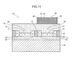
- FIG. 11 is a cross-section illustrating configuration of a semiconductor device 101 according to a second exemplary embodiment of the present disclosure.
- the semiconductor device 101 according to the second exemplary embodiment differs from the semiconductor device 100 according to the first exemplary embodiment described above in that side faces of the filter film 40 are covered by a light-shielding film 60 that blocks ultraviolet rays.
- TiN titanium nitride
- the light-shielding film 60 may, for example, be formed as follows. Note that in the following explanation, a case in which TiN is employed as the material of the light-shielding film 60 is given as an example. After completing the patterning of the filter film 40 , TiN is deposited on the upper face of the insulator layer 14 and the upper face and side faces of the filter film 40 using a sputtering process or the like. Then, the portion of the TiN covering the upper face of the insulator layer 14 and the portion of the TiN covering the upper face of the filter film 40 are removed using dry etching. The portion of the TiN covering the side faces of the filter film 40 is not removed in the dry etching and is left behind. The light-shielding film 60 that covers the side faces of the filter film 40 is thereby formed.
- Covering the side faces of the filter film 40 with a light-shielding film 60 that blocks ultraviolet rays in this manner enables ultraviolet rays that are incident to, and enter, the filter film 40 before being refracted and reflected so as to radiate out of the filter film 40 to be prevented from being incident to the adjacent second photodiode 30 .
- Providing the light-shielding film 60 to the side faces of the filter film 40 can also prevent ultraviolet rays from being incident to, and entering, the filter film 40 from the side faces, and enables the filtering function to be effectively realized by the filter film 40 .
- the semiconductor device 101 according to the second exemplary embodiment of the present disclosure enables UV-A waves and UV-B waves to be separated more precisely than hitherto.
- FIG. 12 is a cross-section illustrating configuration of a semiconductor device 102 according to a third exemplary embodiment of the present disclosure.
- the semiconductor device 102 according to the third exemplary embodiment differs from the semiconductor device 100 according to the first exemplary embodiment described above in that a filter film 50 that transmits UV-B waves with a higher transmittance than UV-A waves is provided to the light incidence side of the second photodiode 30 .
- the semiconductor device 102 according to the third exemplary embodiment is similar to the semiconductor device 100 according to the first exemplary embodiment in that the filter film 40 that transmits UV-A waves with a higher transmittance than UV-B waves is provided to the light incidence side of the first photodiode 20 .
- the filter film 50 is configured similarly to the filter film 40 .
- the filter film 50 has a stacked structure of alternatingly stacked high refractive index layers 51 having a relatively high refractive index and low refractive index layers 52 having a relatively low refractive index.
- a high refractive index layer 51 is placed adjacent to the insulator layer 14 , and there are five high refractive index layers 51 and four low refractive index layers 52 ; however, the filter film 50 is not limited to such configuration.
- a low refractive index layer 52 may be placed adjacent to the insulator layer 14 , and the number of high refractive index layers 51 and low refractive index layers 52 may be modified as appropriate.
- the difference between the refractive indexes of the high refractive index layers 51 and the low refractive index layers 52 is preferably 0.4 or greater, and the refractive index of the high refractive index layers 51 is preferably 2 or less.
- a silicon nitride film (Si 3 N 4 ), which has a refractive index of approximately 1.8, may be suitably employed as the material of the high refractive index layers 51 .
- the filter film 50 is configured such that the optical path length in each of the high refractive index layers 51 and the low refractive index layers 52 is one fourth of the central wavelength ⁇ ca of the UV-A waves.
- the phases of the UV-A waves that are incident to the filter film 50 and reflected at the interfaces between the high refractive index layers 51 and the low refractive index layers 52 are in-phase such that the UV-A waves reinforce one another, while UV-A waves that proceed in the transmission direction are attenuated.
- the filter film 50 configured as above can be provided with a wavelength selectivity that transmits UV-B waves with a higher transmittance than UV-A waves.
- the filter film 50 can be provided with a wavelength selectivity that suppresses UV-A wave transmittance to a specific value or lower.
- the standard value for the layer thickness d 3 of the high refractive index layers 51 is calculated to be 50 nm using Equation (8)
- the standard value for the layer thickness d 4 of the low refractive index layers 52 is calculated to be 64.3 nm using Equation (9).
- the filtering function of the filter film 50 to suppress the UV-A wave transmittance to a specific value or lower is effectively realized by determining the range for the layer thickness d 3 of the high refractive index layers 51 and the range for the layer thickness d 4 of the low refractive index layers 52 as above.
- Having the layer thicknesses of the high refractive index layers 51 and the low refractive index layers 52 in the filter film 50 be different from the layer thicknesses of the high refractive index layers 41 and the low refractive index layers 42 in the filter film 40 provides the filter film 50 with a different wavelength selectivity than the filter film 40 .
- the high refractive index layers 51 and the low refractive index layers 52 configuring the filter film 50 may be formed as films using a plasma CVD process, similarly to the filter film 40 .
- the formation of the high refractive index layers 51 and the low refractive index layers 52 as films may be performed after patterning the filter film 40 .
- the patterning of the filter film 50 may employ a known lift-off process.
- FIG. 13 is a graph illustrating results from a simulation of transmittance-wavelength characteristics in the filter film 50 , for a case in which the layer thickness of the high refractive index layers 51 was set to 50 nm, and the layer thickness of the low refractive index layers 52 was set to 60 nm. Note that the refractive index of the high refractive index layers 51 was set to 1.8 and the refractive index of the low refractive index layers 52 was set to 1.4.
- photocurrent output from the first and second photodiodes 20 , 30 is processed in the signal processing system illustrated in FIG. 7 as follows.
- the analog-digital converter 206 generates a digital value D 1 that accords with the photocurrent output from the first photodiode 20 and a digital value D 2 that accords with the photocurrent output from the second photodiode 30 .
- the digital value D 1 represents the intensity of ultraviolet rays from which the UV-B wave component has been removed by the filter film 40 .
- the digital value D 1 represents the intensity of ultraviolet rays that predominantly include UV-A waves.
- the digital value D 2 represents the intensity of ultraviolet rays from which the UV-A wave component has been removed by the filter film 50 .
- the digital value D 2 represents the intensity of ultraviolet rays that predominantly include UV-B waves.
- the analog-digital converter 206 supplies the digital value D 1 and the digital value D 2 to the MCU 208 via the interface circuit 207 .
- the MCU 208 calculates a UV index I UV using the procedure demonstrated below based on the digital value D 1 and the digital value D 2 supplied via the interface circuit 207 .
- FIG. 14 is a flowchart illustrating a calculation procedure for the UV index I UV of the MCU 208 according to the present exemplary embodiment.
- the MCU 208 calculates a UV-A wave component I UVA of the UV index as expressed by Equation (12) below.
- I UVA c 1 ⁇ 6.68 ⁇ 10 ⁇ 4 ⁇ D 1 (12)
- the MCU 208 calculates a UV-B wave component I UVB of the UV index as expressed by Equation (13) below.
- I UVB c 2 ⁇ 3.08 ⁇ 10 ⁇ 3 ⁇ D 2 (13)
- Equation (12) and Equation (13) are constants determined in accordance with properties of the operational amplifiers 201 , 203 and with the areas of the first and second photodiodes 20 , 30 .
- the MCU 208 calculates the UV index I UV as expressed by Equation (14) below.
- I UV I UVA +I UVB (14)
- the semiconductor device 102 according to the third exemplary embodiment of the present disclosure enables UV-A waves and UV-B waves to be separated more precisely than hitherto.
- the semiconductor device 102 according to the third exemplary embodiment of the present disclosure can lessen the arithmetic processing load on the MCU 208 compared to the semiconductor device 100 according to the first exemplary embodiment, due to photocurrent based on UV-A waves being output from the first photodiode 20 and photocurrent based on UV-B waves being output from the second photodiode 30 .
- step S1 of FIG. 8 can be omitted in the MCU 208 .
- the semiconductor device 102 according to the third exemplary embodiment of the present disclosure can reduce strain (stress) arising in the semiconductor layer 12 compared to a case in which a filter film is only provided to one of the photodiodes, since filter films are respectively provided to the light incidence side of both the first photodiode 20 and the second photodiode 30 .
- a light-shielding film that blocks ultraviolet rays may also be provided to the side faces of the filter film 40 and the filter film 50 of the semiconductor device 102 , similarly to the semiconductor device 101 according to the second exemplary embodiment.
- FIG. 15 is a cross-section illustrating a configuration of a semiconductor device 103 according to a fourth exemplary embodiment of the present disclosure.
- the configuration of a filter film 40 A provided to the light incidence side of the first photodiode 20 in semiconductor device 103 according to the fourth exemplary embodiment differs from the configuration of the filter film 40 provided to the semiconductor device 100 according to the first exemplary embodiment of the present disclosure as described above.
- the filter film 40 A differs from the filter film 40 provided to the semiconductor device 100 according to the first exemplary embodiment described above in that it further includes a thick film layer 43 that is thicker than the layer thicknesses of the high refractive index layers 41 and the low refractive index layers 42 .
- the thick film layer 43 preferably has a layer thickness that is from approximately 2 to approximately 2.5 times the layer thicknesses of the high refractive index layers 41 and the low refractive index layers 42 .
- the thickness of the thick film layer 43 may be set to approximately 100 nm, for example.
- the thick film layer 43 preferably has the same refractive index as the low refractive index layers 42 .
- the thick film layer 43 may be formed from the same silicon oxide film (SiO 2 ) as the low refractive index layers 42 .
- the thick film layer 43 is also preferably disposed at the uppermost portion of the filter film 40 A (namely, a light incidence side end portion).
- the filter film 40 A configured as above is wavelength selective, transmitting UV-A waves with a higher transmittance than UV-B waves, similarly to the filter film 40 according to the first exemplary embodiment.
- Providing the thick film layer 43 to the filter film 40 A enables the ability to transmit UV-A waves to be improved compared to the filter film 40 according to the first exemplary embodiment not provided with the thick film layer 43 .
- FIG. 16A is a graph illustrating results from a simulation of transmittance-wavelength characteristics and reflectance-wavelength characteristics in the filter film 40 according to the first exemplary embodiment not provided with a thick film layer.
- FIG. 16B is a graph illustrating results from a simulation of transmittance-wavelength characteristics and reflectance-wavelength characteristics in the filter film 40 A according to the fourth exemplary embodiment provided with the thick film layer 43 .
- the layer thickness of the high refractive index layers 41 was set to 45 nm
- the layer thickness of the low refractive index layers 42 was set to 40 nm
- the refractive index of the high refractive index layers 41 was set to 1.8
- the refractive index of the low refractive index layers 42 was set to 1.4.
- the layer thickness of the thick film layer 43 was set to 100 nm
- the refractive index of the thick film layer 43 was set to 1.4, the same as that of the low refractive index layers 42 .
- the thick film layer 43 is also disposed at the uppermost portion of the filter film 40 A (the light incidence side end portion).
- transmittance in the vicinity of the 400 nm wavelength, this being the UV-A wave wavelength region is reduced, and reflectance in this wavelength region is at least 0.3.
- transmittance in the vicinity of the 400 nm wavelength, this being the UV-A wave wavelength region is not reduced, and reflectance in this wavelength region is suppressed to 0.1 or less.
- the filter film 40 A having the thick film layer 43 can improve the ability to transmit UV-A waves, compared to the filter film 40 not provided with the thick film layer 43 .
- the UV-B wave component I UVB of the UV index is calculated from the difference between the output of the second photodiode 30 and the output of the first photodiode 20 , as described above, and there is preferably no difference in sensitivity toward UV-A waves between the first photodiode 20 and the second photodiode 30 .
- the filter film 40 A having the thick film layer 43 can decrease the difference in sensitivity toward UV-A waves between the first photodiode 20 and the second photodiode 30 , and the UV index can be calculated more accurately.
Abstract
A semiconductor device that includes: a pair of photoelectric transducers that output photocurrent that accords with an intensity of received light; and a first filter film that is provided to a light incidence side of one out of the pair of photoelectric transducers, that is configured by alternatingly stacking high refractive index layers and low refractive index layers having mutually different refractive indexes, and that transmits one out of either UV-A waves or UV-B waves included in ultraviolet rays with a higher transmittance than the other out of the UV-A waves and the UV-B waves.
Description
This application is based on and claims priority under 35 USC 119 from Japanese Patent Application No. 2015-209226 filed on Oct. 23, 2015, the disclosure of which is incorporated by reference herein.
Technical Field
The present disclosure relates to a semiconductor device and a semiconductor device manufacturing method.
Related Art
As the amount of ultraviolet radiation increases due to destruction of the ozone layer, there is growing concern today over the effect of the ultraviolet rays in sunlight on the human body and the environment.
Ultraviolet rays are classified into long-wavelength ultraviolet rays (UV-A: approximate wavelength of from 320 nm to 400 nm), medium-wavelength ultraviolet rays (UV-B: approximate wavelength of from 280 nm to 320 nm), and short-wavelength ultraviolet rays (UV-C: approximate wavelength of 280 nm and below), with each of these wavelength regions having a different effect on the human body and the environment. UV-A waves cause darkening of the skin, reach the dermis, and are a cause of skin aging. UV-B waves cause inflammation of the skin and may lead to skin cancer. UV-C waves have a strong germicidal effect, but UV-C waves are absorbed by the ozone layer and do not reach the surface of the earth.
Rapid notification of the daily amount of ultraviolet radiation is a matter of importance when it comes to protecting the human body. The UV index, which is an indicator of the amount of ultraviolet radiation, was introduced in 1995. The UV index is a measure of the relative impact on the human body, and may be calculated using the CIE action spectrum defined by the CIE (Commission Internationale de l'Éclairage/International Commission on Illumination).
Japanese Patent Application Laid-Open (JP-A) No. 2008-251709 proposes an ultraviolet ray receiving element capable of separating and detecting quantities of ultraviolet rays in two wavelength regions, UV-A waves and UV-B waves, so as to simplify the derivation of the UV index. This ultraviolet ray receiving element includes a silicon semiconductor layer having a thickness of from 3 nm to 36 nm formed above an insulating layer, lateral PN-junction type first and second photodiodes formed in the silicon semiconductor layer, an interlayer insulating film formed above the silicon semiconductor layer, a first filter layer configured from silicon nitride that is formed above the interlayer insulating film above the first photodiode and that transmits light having a wavelength in the UV-B wave wavelength region or longer, and a second filter layer configured from silicon nitride that is formed above the interlayer insulating film above the second photodiode and that transmits light having a wavelength in the UV-A wave wavelength region or longer.
Japanese Patent Application Laid-Open (JP-A) No. 2009-176835 describes an ultraviolet sensor including a filter film configured from a silicon nitride film that is formed on an interlayer insulating film above one photodiode and that transmits light having a wavelength in the UV-A wave wavelength region or longer, and a sealing layer that covers the interlayer insulating film and the filter film above another photodiode and that transmits light having a wavelength in the UV-B wave wavelength region or longer.
International Publication Pamphlet (WO) No. 2012/137539 describes an ultraviolet sensor including a filter on the light receiving face side of a light receiving element that transmits UV-A waves and UV-B waves.
The filter is configured by a multilayer film of alternatingly stacked low refractive index material and high refractive index material.
In JP-A2008-251709 and JP-A2009-176835, filters are configured using a single layer of silicon nitride film that, of UV-A waves and UV-B waves, blocks the UV-B waves and transmits the UV-A waves.
As illustrated in FIG. 1 , providing a filter film formed from a single layer of silicon nitride film reduces sensitivity toward not only UV-B waves (approximate wavelength of from 280 nm to 320 nm), but also UV-A waves (approximate wavelength of from 320 nm to 400 nm). Namely, precise separation of UV-A waves and UV-B waves is considered to be difficult using a filter film formed from a single layer of silicon nitride film.
The present disclosure has been arrived at in consideration of the above circumstances, and has an objective of providing a semiconductor device and a semiconductor device manufacturing method that are capable of separating UV-A waves and UV-B waves more precisely than hitherto.
A semiconductor device according to the present disclosure includes a pair of photoelectric transducers that output photocurrent that accords with an intensity of received light and a first filter film. The first filter film is provided to a light incidence side of one out of the pair of photoelectric transducers, is configured by alternatingly stacking high refractive index layers and low refractive index layers having mutually different refractive indexes, and transmits one out of either UV-A waves or UV-B waves included in ultraviolet rays with a higher transmittance than the other out of the UV-A waves and the UV-B waves.
A semiconductor device manufacturing method according to the present disclosure includes a process of forming a pair of photoelectric transducers on a semiconductor layer, and a process of forming a first filter film on a light incidence side of one out of the pair of photoelectric transducers. The first filter film is configured by alternatingly stacking high refractive index layers and low refractive index layers having mutually different refractive indexes, and transmits one out of either UV-A waves or UV-B waves with a higher transmittance than the other out of the UV-A waves and the UV-B waves.
The semiconductor device and the semiconductor device manufacturing method according to the present disclosure enable UV-A waves and UV-B waves to be separated more precisely than hitherto.
Exemplary embodiments of the present disclosure will be described in detail based on the following figures, wherein:
Explanation follows regarding exemplary embodiments of the present disclosure, with reference to the figures. Note that in each of the drawings, configuration elements and portions that are the same or that are equivalent are appended with the same reference numerals, and duplicate explanation is omitted as appropriate.
The first photodiode 20 includes a cathode 22 formed from an n-type semiconductor having a relatively high concentration of impurities, an anode 23 formed from a p-type semiconductor having a relatively high concentration of impurities, and a low concentration region 21 that is formed from a p-type semiconductor having a relatively low concentration of impurities and is provided between the cathode 22 and the anode 23. The low concentration region 21 is the principle light receiving region in the first photodiode 20. The thickness of the low concentration region 21 is thinner than that of the cathode 22 and the anode 23, and is set to 36 nm or less, for example. Setting the thickness of the low concentration region 21 forming the light receiving region to 36 nm or less enables the first photodiode 20 to be imparted with a reduced sensitivity toward light having a longer wavelength than ultraviolet rays including UV-A waves and UV-B waves, and the first photodiode 20 to be provided with a spectral sensitivity suitable for an ultraviolet sensor.
The second photodiode 30 has a similar configuration to the first photodiode 20. Namely, the second photodiode 30 includes a cathode 32 formed from an n-type semiconductor having a relatively high concentration of impurities, an anode 33 formed from a p-type semiconductor having a relatively high concentration of impurities, and a low concentration region 31 formed from a p-type semiconductor having a relatively low concentration of impurities provided between the cathode 32 and the anode 33. The low concentration region 31 is the principle light receiving region in the second photodiode 30. The thickness of the low concentration region 31 is thinner than that of the cathode 32 and the anode 33, and is set to 36 nm or less, for example.
The first photodiode 20 and the second photodiode 30 are covered by an insulator layer 14 formed from an insulator such as SiO2. Plural wiring layers may be provided within the insulator layer 14. In cases in which there are four wiring layers, for example, the thickness of the insulator layer 14 is set to approximately 4 μm.
A filter film 40 that covers an area above the first photodiode 20 is provided to the surface of the insulator layer 14. Namely, the filter film 40 is provided to the light incidence side of the first photodiode 20. In the present exemplary embodiment the filter film 40 is wavelength selective, transmitting UV-A waves with a higher transmittance than UV-B waves. In other words, for UV-A waves and UV-B waves, the filter film 40 is wavelength selective, reflecting UV-B waves with a greater reflectance than UV-A waves.
The filter film 40 has a stacked structure of alternatingly stacked high refractive index layers 41 having a relatively high refractive index and low refractive index layers 42 having a relatively low refractive index. In the present exemplary embodiment, as illustrated in FIG. 2 , a high refractive index layer 41 is placed adjacent to the insulator layer 14, and there are five high refractive index layers 41 and four low refractive index layers 42. However, the filter film 40 is not limited to such configuration. Namely, a low refractive index layer 42 may be placed adjacent to the insulator layer 14, and the number of high refractive index layers 41 and low refractive index layers 42 may be modified as appropriate.
The difference between the refractive indexes of the high refractive index layers 41 and the low refractive index layers 42 is preferably 0.4 or greater, and the refractive index of the high refractive index layers 41 is preferably 2 or less. A silicon dioxide film (SiO2), which has a refractive index of about 1.4, may be suitably employed as the material of the low refractive index layers 42. A silicon nitride film (Si3N4), which has a refractive index of approximately 1.8, may be suitably employed as the material of the high refractive index layers 41.
Denoting the refractive index of the high refractive index layers 41 as n1, the refractive index of the low refractive index layers 42 as n2, and the central wavelength of the UV-B waves toward which the filter film 40 has a relatively low transmittance as λcb (approximately 300 nm), it preferable to determine standard values for the layer thickness d1 of the high refractive index layers 41 and the layer thickness d2 of the low refractive index layers 42 such that Equation (1) and Equation (2) given below are respectively satisfied.
n 1 ·d 1=λcb/4 (1)
n 2 ·d 2=λcb/4 (2)
n 1 ·d 1=λcb/4 (1)
n 2 ·d 2=λcb/4 (2)
Namely, the filter film 40 is configured such that the optical path length in each of the high refractive index layers 41 and the low refractive index layers 42 is one fourth of the central wavelength λcb of the UV-B waves. By determining the layer thickness d1 of the high refractive index layers 41 and the layer thickness d2 of the low refractive index layers 42 such that Equation (1) and Equation (2) are satisfied, the phases of UV-B waves that are incident to the filter film 40 and reflected at the interfaces between the high refractive index layers 41 and the low refractive index layers 42 are in-phase such that the UV-B waves reinforce one another, while UV-B waves that proceed in the transmission direction are attenuated. Namely, the filter film 40 configured as above can be provided with a wavelength selectivity that transmits UV-A waves with a higher transmittance than UV-B waves. In other words, the filter film 40 configured as described above can be provided with a wavelength selectivity in which UV-B wave transmittance is suppressed to a specific value or lower.
In a case in which the central wavelength λcb of the UV-B waves is 300 nm, the refractive index n1 of the high refractive index layers 41 is 1.8, and the refractive index n2 of the low refractive index layers 42 is 1.4, the standard value for the layer thickness d1 of the high refractive index layers 41 is calculated to be 41.6 nm using Equation (1), and the standard value for the layer thickness d2 of the low refractive index layers 42 is calculated to be 53.6 nm using Equation (2).
When a range of wavelengths λb of the UV-B waves for which the filter film 40 has a relatively low transmittance is λb1≦λb≦λb2 (λb1 is approximately 280 nm, and λb2 is approximately 320 nm), it is preferable to determine a range for the layer thickness d1 of the high refractive index layers 41 and a range for the layer thickness d2 of the low refractive index layers 42 such that Equation (3) and Equation (4) given below are respectively satisfied.
λb1/(4 ·n 1)≦d 1≦λb2/(4·n 1) (3)
λb1/(4·n 2)≦d 2≦λb2/(4·n 2) (4)
λb1/(4 ·n 1)≦d 1≦λb2/(4·n 1) (3)
λb1/(4·n 2)≦d 2≦λb2/(4·n 2) (4)
The filtering function of the filter film 40 to suppress the UV-B wave transmittance to a specific value or lower is effectively realized by determining the range for the layer thickness d1 of the high refractive index layers 41 and the range for the layer thickness d2 of the low refractive index layers 42 as above.
As illustrated in FIG. 3 , it was confirmed that it is possible to reduce the transmittance of the filter film 40 in the UV-B wave wavelength region (from 280 nm to 320 nm) without impacting the transmittance of the filter film 40 in the UV-A wave wavelength region (from 320 nm to 400 nm) for each of the cases in which the layer thickness of the high refractive index layers 41 was respectively set to 40 μm, 45 μm, or 50 μm. It was also confirmed that increasing the layer thickness of the high refractive index layers 41 shifts the wavelengths for which the filter film 40 suppresses transmittance to a specific value or lower, shifting the wavelengths toward the longer wavelength side.
In the semiconductor device 100 according to the present exemplary embodiment, a filter film is not provided to the light incidence side of the second photodiode 30. Namely, the second photodiode 30 receives both UV-A waves and UV-B waves.
Explanation follows regarding a manufacturing method of the semiconductor device 100 according to the present exemplary embodiment. FIGS. 4A to 4C , FIG. 5A , FIG. 5B , FIG. 6A , and FIG. 6B are cross-sections illustrating an example of a manufacturing method of the semiconductor device 100.
Firstly, a SOI substrate 1 in which the substrate layer 10, the insulator layer 11, and the semiconductor layer 12 are stacked is prepared (FIG. 4A ). In the present exemplary embodiment, the semiconductor layer 12 is formed from p-type silicon. The semiconductor layer 12 then undergoes ion implantation processing to give the impurity concentrations in the low concentration regions 21, 31 of the first and second photodiodes 20, 30.
Next, the element isolator 13 that surrounds formation regions of the first photodiode 20 and the second photodiode 30 is formed in the semiconductor layer 12 (FIG. 4B ). The element isolator 13 may be formed using a known shallow trench isolation (STI) process, for example. The STI process includes a process of forming trenches in the semiconductor layer 12 that reach to the insulator layer 11, a process of filling the trenches in with an insulator such as SiO2, and a process of removing unwanted insulator that has been deposited on the surface of the semiconductor layer 12 by chemical mechanical polishing (CMP). Note that the element isolator 13 may also be formed using a known local oxidation of silicon (LOCOS) process.
Next, the semiconductor layer 12 is partially etched to form respective depressions 12A in regions that correspond to the low concentration regions 21, 31 of the first and second photodiodes 20, 30. The thickness in the regions that correspond to the low concentration regions 21, 31 of the semiconductor layer 12 is thereby thinned to approximately 36 nm (FIG. 4C ). Setting the thickness of the regions that correspond to the low concentration regions 21, 31 to 36 nm or less enables the first and second photodiodes 20, 30 to be imparted with a reduced sensitivity toward light having a longer wavelength than ultraviolet rays including UV-A waves and UV-B waves, and enables the first and second photodiodes 20, 30 having a spectral sensitivity suitable for an ultraviolet sensor to be obtained.
Next, the cathodes 22, 32 of the first and second photodiodes 20, 30 are formed by implanting group V elements such as phosphorus or arsenic into the semiconductor layer 12 using a known ion implantation process. Then, the anodes 23, 33 of the first and second photodiodes 20, 30 are formed by implanting group III elements such as boron into the semiconductor layer 12 using a known ion implantation process. In the first photodiode 20, the low concentration region 21 is disposed at the position where the depression 12A is formed, and the cathode 22 and the anode 23 are disposed at positions sandwiching the low concentration region 21. In the second photodiode 30, the low concentration region 31 is disposed at the position where the depression 12A is formed, and the cathode 32 and the anode 33 are disposed at positions sandwiching the low concentration region 31 (FIG. 5A ).
Next, using a CVD process, the insulator layer 14, which is formed from an insulator such as SiO2, is formed on the surface of the semiconductor layer 12 that has been formed with the first and second photodiodes 20, 30 (FIG. 5B ). Plural wiring layers may be provided within the insulator layer 14. In cases in which there are four wiring layers, for example, the thickness of the insulator layer 14 is set to approximately 4 μm.
Next, the high refractive index layers 41 and the low refractive index layers 42 are alternatingly stacked on the surface of the insulator layer 14 to form the filter film 40 (FIG. 6A ).
The high refractive index layers 41 may be formed from silicon nitride films (Si3N4) that are formed using a plasma CVD process employing SiH4 (silane) and NH3 (ammonia) as the source gases, for example. The refractive index of the high refractive index layers 41 can be controlled by controlling the flow rate of SiH4. In the present exemplary embodiment, the flow rate of SiH4 is set to 1.69×10⁻² Pa·m3/sec and the flow rate of NH3 is set to 1.27×10⁻¹ Pa·m3/sec such that the high refractive index layers 41 formed from the silicon nitride films have a refractive index of approximately 1.8.
The low refractive index layers 42 may be formed from silicon dioxide films (SiO2) that are formed using a plasma CVD process employing tetraethyl orthosilicate (TEOS) and oxygen (O2) as the source gases. The low refractive index layers 42 formed from the silicon dioxide films have a refractive index of approximately 1.4.
The high refractive index layers 41 and the low refractive index layers 42 are formed such that the layer thickness d1 of the high refractive index layers 41 and the layer thickness d2 of the low refractive index layers 42 respectively satisfy Equation (3) and Equation (4) above. Thus, the filter film 40 is formed having a wavelength selectivity that suppresses the UV-B wave transmittance to a specific value or lower.
Next, patterning of the filter film 40 is performed using etching so as to remove portions of the filter film 40 covering the area above the second photodiode 30 (FIG. 6B ). Note that the patterning of the filter film 40 may be performed using a lift-off process.
The photocurrent output from the first photodiode 20 is converted to a voltage by a transimpedance amplifier 211 configured including the operational amplifier 201 and the resistance element 202. Namely, a voltage of a magnitude proportionate to the magnitude of the photocurrent output from the first photodiode 20 is output from the transimpedance amplifier 211.
Similarly, the photocurrent output from the second photodiode 30 is converted to a voltage by a transimpedance amplifier 212 configured including the operational amplifier 203 and the resistance element 204. Namely, a voltage of a magnitude proportionate to the magnitude of the photocurrent output from the second photodiode 30 is output from the transimpedance amplifier 212.
The multiplexer 205 sequentially supplies the voltages output from the transimpedance amplifiers 211, 212 to the analog-digital converter 206.
The analog-digital converter 206 converts the voltage supplied from the multiplexer 205 to a digital signal. Namely, the analog-digital converter 206 generates a digital value D1 that accords with the photocurrent output from the first photodiode 20 and a digital value D2 that accords with the photocurrent output from the second photodiode 30. The digital value D1 represents the intensity of ultraviolet rays from which the UV-B wave component has been removed by the filter film 40. In other words, the digital value D1 represents the intensity of ultraviolet rays that predominantly include UV-A waves. In contrast thereto, the digital value D2 represents the intensity of ultraviolet rays that include both UV-A waves and UV-B waves. The analog-digital converter 206 supplies the digital value D1 and the digital value D2 to the MCU 208 via the interface circuit 207.
The MCU 208 calculates a UV index IUV using the procedure demonstrated below based on the digital value D1 and the digital value D2 supplied via the interface circuit 207. FIG. 8 is a flowchart illustrating a calculation procedure for the UV index IUV of the MCU 208.
At step S1, the MCU 208 subtracts the digital value D1 from the digital value D2 to derive a digital value D3 (D3=D2−D1). Digital value D3 represents the intensity of ultraviolet rays that predominantly include UV-B waves.
At step S2, the MCU 208 calculates a UV-A wave component IUVA of the UV index as expressed by Equation (5) below.
I UVA −c 1×6.68×10−4 ×D 1 (5)
I UVA −c 1×6.68×10−4 ×D 1 (5)
At step S3, the MCU 208 calculates a UV-B wave component IUVB of the UV index as expressed by Equation (6) below.
I UVB =c 2×3.08×10−3 ×D 3 (6)
I UVB =c 2×3.08×10−3 ×D 3 (6)
Note that in Equation (5) and Equation (6), c1 and c2 are constants determined in accordance with properties of the operational amplifiers 201, 203 and with the areas of the first and second photodiodes 20, 30.
At step S4, the MCU 208 calculates the UV index IUV as expressed by Equation (7) below.
I UV =I UVA +I UVB (7)
I UV =I UVA +I UVB (7)
As illustrated in FIG. 9 , the sensitivity toward UV-A waves of the first photodiode 20 having the filter film 40 on the light incidence side was similar to that of the second photodiode 30 not provided with a filter film. In contrast thereto, the sensitivity toward UV-B waves of the first photodiode 20 was notably lower than that of the second photodiode 30. Namely, providing the filter film 40 enabled UV-A waves to be transmitted with a higher transmittance than UV-B waves. Configuring the filter film 40 with stacked layers in this manner gives similar waveform shapes in one out of the UV-A wave wavelength region or the UV-B wave wavelength region and a large difference in waveform shapes in the other out of the UV-A wave wavelength region or the UV-B wave wavelength region. This thereby makes it possible to find the desired UV index with simple subtractive processing. As a result, rapid processing is possible even with a compact microprocessor capable of being run at low power, for example, and also enables operation on a wearable device such as a watch.
As is clear from the above explanation, in the semiconductor device 100 according to the present exemplary embodiment, the filter film 40 is configured by alternatingly stacking high refractive index layers and low refractive index layers formed with layer thicknesses that satisfy Equation (3) and Equation (4) above. Accordingly, the filter film 40 can be provided with a wavelength selectivity that transmits UV-A waves with a higher transmittance than UV-B waves. As is clear from comparing FIG. 1 and FIG. 9 , the filter film 40 according to the present exemplary embodiment enables wavelength selectivity to be greatly improved compared to a conventional filter film formed from a single layer of silicon nitride film. Namely, the semiconductor device 100 according to an exemplary embodiment of the present disclosure and the manufacturing method thereof enable UV-A waves and UV-B waves to be separated more precisely than hitherto.
Setting the difference between the refractive indexes of the high refractive index layers 41 and the low refractive index layers 42 to 0.4 or greater enables the function of the filter film 40 to reflect UV-B waves to be sufficiently realized. Setting the refractive index of the high refractive index layers 41 to 2 or less also enables the transmittance for UV-A waves to be secured.
In the semiconductor device 100 according to the present exemplary embodiment, strain (stress) arising in the semiconductor layer 12 increases as the number of high refractive index layers 41 and low refractive index layers 42 becomes greater, due to the filter film 40 only covering the first photodiode 20 out of the first and second photodiodes 20, 30, and this is liable to affect the characteristics of the first and second photodiodes 20, 30. With the semiconductor device 100 according to the present exemplary embodiment, by deriving the intensity of ultraviolet rays that predominantly include UV-B waves by subtracting the digital value D1, which is based on photocurrent of the first photodiode 20, from the digital value D2, which is based on photocurrent of the second photodiode 30, it is possible to effectively separate UV-A waves and UV-B waves even in cases in which the number of high refractive index layers 41 and low refractive index layers 42 is relatively low (for example, from five to ten layers). This thereby avoids the issue described above of strain (stress) arising in the semiconductor layer 12.
In the present exemplary embodiment, explanation has given regarding a case in which the filter film 40 that transmits UV-A waves with a higher transmittance than UV-B waves is provided to the light incidence side of the first photodiode 20; however, there is no limitation thereto. Namely, a filter film that transmits UV-B waves with a higher transmittance than UV-A waves may be provided to the light incidence side of the first photodiode 20. In such a case, the layer thicknesses of the high refractive index layers and the low refractive index layers configuring the filter film are set in conformance with Equation (3) and Equation (4) above. In Equation (3) and Equation (4), λb1 and λb2 are also respectively set to the lower limit value (320 nm) and the upper limit value (400 nm) of the UV-A wave wavelengths. Additionally, in the case in which a filter film that transmits UV-B waves with a higher transmittance than UV-A waves is employed, digital values D1 and D3 are interchanged in Equation (5) and Equation (6) above when calculating the UV index.
In the present exemplary embodiment, although a case in which silicon nitride films are employed as the high refractive index layers 41 has been given as an example, HfO2 (hafnium oxide) may be employed as the high refractive index layers 41.
The light-shielding film 60 may, for example, be formed as follows. Note that in the following explanation, a case in which TiN is employed as the material of the light-shielding film 60 is given as an example. After completing the patterning of the filter film 40, TiN is deposited on the upper face of the insulator layer 14 and the upper face and side faces of the filter film 40 using a sputtering process or the like. Then, the portion of the TiN covering the upper face of the insulator layer 14 and the portion of the TiN covering the upper face of the filter film 40 are removed using dry etching. The portion of the TiN covering the side faces of the filter film 40 is not removed in the dry etching and is left behind. The light-shielding film 60 that covers the side faces of the filter film 40 is thereby formed.
Covering the side faces of the filter film 40 with a light-shielding film 60 that blocks ultraviolet rays in this manner enables ultraviolet rays that are incident to, and enter, the filter film 40 before being refracted and reflected so as to radiate out of the filter film 40 to be prevented from being incident to the adjacent second photodiode 30. Providing the light-shielding film 60 to the side faces of the filter film 40 can also prevent ultraviolet rays from being incident to, and entering, the filter film 40 from the side faces, and enables the filtering function to be effectively realized by the filter film 40.
Moreover, similarly to the semiconductor device 100 according to the first exemplary embodiment, the semiconductor device 101 according to the second exemplary embodiment of the present disclosure enables UV-A waves and UV-B waves to be separated more precisely than hitherto.
The filter film 50 is configured similarly to the filter film 40. Namely, the filter film 50 has a stacked structure of alternatingly stacked high refractive index layers 51 having a relatively high refractive index and low refractive index layers 52 having a relatively low refractive index. In the present exemplary embodiment, a high refractive index layer 51 is placed adjacent to the insulator layer 14, and there are five high refractive index layers 51 and four low refractive index layers 52; however, the filter film 50 is not limited to such configuration. Namely, a low refractive index layer 52 may be placed adjacent to the insulator layer 14, and the number of high refractive index layers 51 and low refractive index layers 52 may be modified as appropriate.
The difference between the refractive indexes of the high refractive index layers 51 and the low refractive index layers 52 is preferably 0.4 or greater, and the refractive index of the high refractive index layers 51 is preferably 2 or less. A silicon dioxide film (SiO2), which has a refractive index of approximately 1.4, may be suitably employed as the material of the low refractive index layers 52. A silicon nitride film (Si3N4), which has a refractive index of approximately 1.8, may be suitably employed as the material of the high refractive index layers 51.
Denoting the refractive index of the high refractive index layers 51 as n3, the refractive index of the low refractive index layers 52 as n4, and the central wavelength of the UV-A waves toward which the filter film 50 has a relatively low transmittance as λca (approximately 360 nm), it preferable to determine standard values for the layer thickness d3 of the high refractive index layers 51 and the layer thickness d4 of the low refractive index layers 52 such that Equation (8) and Equation (9) given below are respectively satisfied.
n 3 ·d 3=λca/4 (8)
n 4 ·d 4=λca/4 (9)
n 3 ·d 3=λca/4 (8)
n 4 ·d 4=λca/4 (9)
Namely, the filter film 50 is configured such that the optical path length in each of the high refractive index layers 51 and the low refractive index layers 52 is one fourth of the central wavelength λca of the UV-A waves. By determining the layer thickness d3 of the high refractive index layers 51 and the layer thickness d4 of the low refractive index layers 52 such that Equation (8) and Equation (9) are satisfied, the phases of the UV-A waves that are incident to the filter film 50 and reflected at the interfaces between the high refractive index layers 51 and the low refractive index layers 52 are in-phase such that the UV-A waves reinforce one another, while UV-A waves that proceed in the transmission direction are attenuated. Namely, the filter film 50 configured as above can be provided with a wavelength selectivity that transmits UV-B waves with a higher transmittance than UV-A waves. In other words, the filter film 50 can be provided with a wavelength selectivity that suppresses UV-A wave transmittance to a specific value or lower.
In a case in which λca is 360 nm, n3 is 1.8, and n4 is 1.4, the standard value for the layer thickness d3 of the high refractive index layers 51 is calculated to be 50 nm using Equation (8), and the standard value for the layer thickness d4 of the low refractive index layers 52 is calculated to be 64.3 nm using Equation (9).
When a range of wavelengths λa of the UV-A waves for which the filter film 50 has a relatively low transmittance is λa1≦λa≦λa2 (λa1 is approximately 320 nm, and λa2 is approximately 400 nm), it is preferable to determine a range for the layer thickness d3 of the high refractive index layers 51 and a range for the layer thickness d4 of the low refractive index layers 52 such that Equation (10) and Equation (11) given below are respectively satisfied.
λa1/(4·n 3)≦d 3≦λa2/(4·n 3) (10)
λa1/(4·n 4)≦d 4≦λa2/(4·n 4) (11)
λa1/(4·n 3)≦d 3≦λa2/(4·n 3) (10)
λa1/(4·n 4)≦d 4≦λa2/(4·n 4) (11)
The filtering function of the filter film 50 to suppress the UV-A wave transmittance to a specific value or lower is effectively realized by determining the range for the layer thickness d3 of the high refractive index layers 51 and the range for the layer thickness d4 of the low refractive index layers 52 as above.
Having the layer thicknesses of the high refractive index layers 51 and the low refractive index layers 52 in the filter film 50 be different from the layer thicknesses of the high refractive index layers 41 and the low refractive index layers 42 in the filter film 40 provides the filter film 50 with a different wavelength selectivity than the filter film 40.
The high refractive index layers 51 and the low refractive index layers 52 configuring the filter film 50 may be formed as films using a plasma CVD process, similarly to the filter film 40. The formation of the high refractive index layers 51 and the low refractive index layers 52 as films may be performed after patterning the filter film 40. As an example, the patterning of the filter film 50 may employ a known lift-off process.
As illustrated in FIG. 13 , it was confirmed that it is possible to reduce the transmittance of the filter film 50 in the UV-A wave wavelength region (from 320 nm to 400 nm) without impacting the transmittance of the filter film 50 in the UV-B wave wavelength region (from 280 nm to 320 nm)
In the semiconductor device 102 according to the present exemplary embodiment, photocurrent output from the first and second photodiodes 20, 30 is processed in the signal processing system illustrated in FIG. 7 as follows. The analog-digital converter 206 generates a digital value D1 that accords with the photocurrent output from the first photodiode 20 and a digital value D2 that accords with the photocurrent output from the second photodiode 30. The digital value D1 represents the intensity of ultraviolet rays from which the UV-B wave component has been removed by the filter film 40. In other words, the digital value D1 represents the intensity of ultraviolet rays that predominantly include UV-A waves. In contrast thereto, the digital value D2 represents the intensity of ultraviolet rays from which the UV-A wave component has been removed by the filter film 50. In other words, the digital value D2 represents the intensity of ultraviolet rays that predominantly include UV-B waves. The analog-digital converter 206 supplies the digital value D1 and the digital value D2 to the MCU 208 via the interface circuit 207.
The MCU 208 calculates a UV index IUV using the procedure demonstrated below based on the digital value D1 and the digital value D2 supplied via the interface circuit 207. FIG. 14 is a flowchart illustrating a calculation procedure for the UV index IUV of the MCU 208 according to the present exemplary embodiment.
At step S11, the MCU 208 calculates a UV-A wave component IUVA of the UV index as expressed by Equation (12) below.
I UVA =c 1×6.68×10−4 ×D 1 (12)
I UVA =c 1×6.68×10−4 ×D 1 (12)
At step S12, the MCU 208 calculates a UV-B wave component IUVB of the UV index as expressed by Equation (13) below.
I UVB =c 2×3.08×10−3 ×D 2 (13)
I UVB =c 2×3.08×10−3 ×D 2 (13)
Note that in Equation (12) and Equation (13), c1 and c2 are constants determined in accordance with properties of the operational amplifiers 201, 203 and with the areas of the first and second photodiodes 20, 30.
At step S13, the MCU 208 calculates the UV index IUV as expressed by Equation (14) below.
I UV =I UVA +I UVB (14)
I UV =I UVA +I UVB (14)
As described above, similarly to the semiconductor device 100 according to the first exemplary embodiment, the semiconductor device 102 according to the third exemplary embodiment of the present disclosure enables UV-A waves and UV-B waves to be separated more precisely than hitherto.
The semiconductor device 102 according to the third exemplary embodiment of the present disclosure can lessen the arithmetic processing load on the MCU 208 compared to the semiconductor device 100 according to the first exemplary embodiment, due to photocurrent based on UV-A waves being output from the first photodiode 20 and photocurrent based on UV-B waves being output from the second photodiode 30. Specifically, step S1 of FIG. 8 can be omitted in the MCU 208.
The semiconductor device 102 according to the third exemplary embodiment of the present disclosure can reduce strain (stress) arising in the semiconductor layer 12 compared to a case in which a filter film is only provided to one of the photodiodes, since filter films are respectively provided to the light incidence side of both the first photodiode 20 and the second photodiode 30.
A light-shielding film that blocks ultraviolet rays may also be provided to the side faces of the filter film 40 and the filter film 50 of the semiconductor device 102, similarly to the semiconductor device 101 according to the second exemplary embodiment.
The thick film layer 43 preferably has a layer thickness that is from approximately 2 to approximately 2.5 times the layer thicknesses of the high refractive index layers 41 and the low refractive index layers 42. For example, in a case in which the layer thickness of the high refractive index layers 41 is approximately 45 nm, and the layer thickness of the low refractive index layers 42 is approximately 40 nm, the thickness of the thick film layer 43 may be set to approximately 100 nm, for example.
The thick film layer 43 preferably has the same refractive index as the low refractive index layers 42. Namely, the thick film layer 43 may be formed from the same silicon oxide film (SiO2) as the low refractive index layers 42. The thick film layer 43 is also preferably disposed at the uppermost portion of the filter film 40A (namely, a light incidence side end portion).
The filter film 40A configured as above is wavelength selective, transmitting UV-A waves with a higher transmittance than UV-B waves, similarly to the filter film 40 according to the first exemplary embodiment. Providing the thick film layer 43 to the filter film 40A enables the ability to transmit UV-A waves to be improved compared to the filter film 40 according to the first exemplary embodiment not provided with the thick film layer 43.
As illustrated in FIG. 16A , in to the filter film 40 not provided with a thick film layer, transmittance in the vicinity of the 400 nm wavelength, this being the UV-A wave wavelength region, is reduced, and reflectance in this wavelength region is at least 0.3. In contrast thereto, as illustrated in FIG. 16B , in to the filter film 40A provided with the thick film layer 43, transmittance in the vicinity of the 400 nm wavelength, this being the UV-A wave wavelength region, is not reduced, and reflectance in this wavelength region is suppressed to 0.1 or less.
The filter film 40A having the thick film layer 43 can improve the ability to transmit UV-A waves, compared to the filter film 40 not provided with the thick film layer 43. Note that as the UV-B wave component IUVB of the UV index is calculated from the difference between the output of the second photodiode 30 and the output of the first photodiode 20, as described above, and there is preferably no difference in sensitivity toward UV-A waves between the first photodiode 20 and the second photodiode 30. The filter film 40A having the thick film layer 43 can decrease the difference in sensitivity toward UV-A waves between the first photodiode 20 and the second photodiode 30, and the UV index can be calculated more accurately.
Claims (14)
1. A semiconductor device comprising:
a pair of photoelectric transducers that output photocurrents that correspond to an intensity of received light;
an element isolator that surrounds each of the pair of photoelectric transducers;
a first filter film that is provided at a light incidence side of one of the pair of photoelectric transducers, that is configured by alternatingly stacking high refractive index layers and low refractive index layers having mutually different refractive indexes, and that transmits one of either UV-A waves or UV-B waves included in ultraviolet rays with a higher transmittance than an other of the UV-A waves and the UV-B waves; and
an insulator layer that has a lower face contacting the pair of photoelectric transducers and the element isolator, and an upper face opposing the lower face, the insulator layer covering faces of the pair of photoelectric transducers and the element isolator,
wherein a region of the upper face, corresponding to the light incidence side of an other of the pair of photoelectric transducers, is configured to be exposed.
2. The semiconductor device of claim 1 , wherein the equations
λ1/(4·n 1)≦d 1≦λ2/(4·n 1), and
λ1/(4·n 2)≦d 2≦λ2/(4·n 2)
λ1/(4·n 1)≦d 1≦λ2/(4·n 1), and
λ1/(4·n 2)≦d 2≦λ2/(4·n 2)
are satisfied, where n1 is the refractive index of the high refractive index layers, d1 is a layer thickness of the high refractive index layers, n2 is a refractive index of the low refractive index layers, d2 is a layer thickness of the low refractive index layers, and a range of wavelengths λ for which the first filter film has a lower transmittance, from out of the UV-A waves or the UV-B waves, is λ1≦λ≦λ2.
3. The semiconductor device of claim 1 , wherein a difference between refractive indexes of the low refractive index layers and the high refractive index layers is 0.4 or greater, and the refractive index of the high refractive index layers is 2 or less.
4. The semiconductor device of claim 1 , wherein the first filter film further includes a thick film layer that has a same refractive index as one of either the high refractive index layers or the low refractive index layers, and that is thicker than layer thicknesses of the high refractive index layers and the low refractive index layers.
5. The semiconductor device of claim 4 , wherein the thick film layer is disposed at an uppermost portion of the first filter film.
6. The semiconductor device of claim 4 , wherein the thick film layer has the same refractive index as the low refractive index layers.
7. The semiconductor device of claim 1 , wherein the low refractive index layers include a silicon oxide film, and the high refractive index layers include a silicon nitride film.
8. The semiconductor device of claim 1 , wherein a thickness of respective light receiving regions of the pair of photoelectric transducers is 36 nm or less.
9. The semiconductor device of claim 1 , wherein side faces of the first filter film are covered by a light-shielding film that blocks ultraviolet rays.
10. The semiconductor device of claim 1 , wherein the other of the pair of photoelectric transducers receives both the UV-A waves and the UV-B waves.
11. The semiconductor device of claim 1 , further comprising:
a calculation section configured to calculate an index value representing an intensity of received ultraviolet rays based on photocurrent output from the one of the pair of photoelectric transducers and photocurrent output from the other of the pair of photoelectric transducers.
12. The semiconductor device of claim 11 , wherein the calculation section is configured to calculate, as the index value, a summed value of a first value that corresponds to an intensity of the UV-A waves and a second value that corresponds to an intensity of the UV-B waves.
13. A semiconductor device manufacturing method comprising:
a process of forming a pair of photoelectric transducers on a semiconductor layer;
a process of forming an element isolator that surrounds each of the pair of photoelectric transducers;
a process of forming, on a light incidence side of one of the pair of photoelectric transducers, a first filter film that is configured by alternatingly stacking high refractive index layers and low refractive index layers having mutually different refractive indexes, and that transmits one of either UV-A waves or UV-B waves with a higher transmittance than an other of the UV-A waves and the UV-B waves; and
a process of forming an insulator layer that has a lower face contacting the pair of photoelectric transducers and the element isolator, and an upper face opposing the lower face, the insulator layer covering faces of the pair of photoelectric transducers and the element isolator,
wherein a region of the upper face, corresponding to the light incidence side of an other of the pair of photoelectric transducers, is configured to be exposed.
14. A semiconductor device comprising:
a pair of photoelectric transducers that output photocurrents that correspond to an intensity of received light;
a first filter film that is provided at a light incidence side of one of the pair of photoelectric transducers, that is configured by alternatingly stacking high refractive index layers and low refractive index layers having mutually different refractive indexes, and that transmits UV-A waves included in ultraviolet rays with a higher transmittance than UV-B waves; and
a second filter film that is provided at a light incidence side of an other of the pair of photoelectric transducers, that is configured by alternatingly stacking second high refractive index layers and second low refractive index layers having mutually different refractive indexes, and that transmits the UV-B waves with a higher transmittance than the UV-A waves.
Applications Claiming Priority (2)
| Application Number | Priority Date | Filing Date | Title |
|---|---|---|---|
| JP2015209226A JP2017084875A (en) | 2015-10-23 | 2015-10-23 | Semiconductor device and method of manufacturing semiconductor device |
| JP2015-209226 | 2015-10-23 |
Publications (2)
| Publication Number | Publication Date |
|---|---|
| US20170117421A1 US20170117421A1 (en) | 2017-04-27 |
| US9876126B2 true US9876126B2 (en) | 2018-01-23 |
Family
ID=58559045
Family Applications (1)
| Application Number | Title | Priority Date | Filing Date |
|---|---|---|---|
| US15/296,339 Active US9876126B2 (en) | 2015-10-23 | 2016-10-18 | Semiconductor device and semiconductor device manufacturing method |
Country Status (3)
| Country | Link |
|---|---|
| US (1) | US9876126B2 (en) |
| JP (1) | JP2017084875A (en) |
| CN (1) | CN107068782B (en) |
Families Citing this family (2)
| Publication number | Priority date | Publication date | Assignee | Title |
|---|---|---|---|---|
| KR20180065060A (en) * | 2016-12-06 | 2018-06-18 | 삼성디스플레이 주식회사 | Organic Light Emitting Display Device |
| FR3083644B1 (en) * | 2018-07-09 | 2021-05-14 | St Microelectronics Crolles 2 Sas | IMAGE SENSOR |
Citations (7)
| Publication number | Priority date | Publication date | Assignee | Title |
|---|---|---|---|---|
| US20080111205A1 (en) * | 2006-11-14 | 2008-05-15 | Oki Electric Industry Co., Ltd. | Photodiode |
| JP2008251709A (en) | 2007-03-29 | 2008-10-16 | Oki Electric Ind Co Ltd | Ultraviolet photo-detector and its manufacturing method, and device for measuring ultraviolet dose |
| JP2009176835A (en) | 2008-01-22 | 2009-08-06 | Oki Semiconductor Co Ltd | Ultraviolet sensor and method of manufacturing the same |
| US20100084678A1 (en) * | 2007-05-30 | 2010-04-08 | Osram Opto Semiconductors Gmbh | Luminescent Diode Chip |
| US20110204233A1 (en) * | 2009-06-30 | 2011-08-25 | Avago Technologies Ecbu (Singapore) Pte. Ltd. | Infrared Attenuating or Blocking Layer in Optical Proximity Sensor |
| US20120199826A1 (en) * | 2010-10-14 | 2012-08-09 | Rohm Co., Ltd. | Photodetection device and optical filter used therein |
| WO2012137539A1 (en) | 2011-04-06 | 2012-10-11 | アルプス電気株式会社 | Ultraviolet sensor |
Family Cites Families (9)
| Publication number | Priority date | Publication date | Assignee | Title |
|---|---|---|---|---|
| JP2002033503A (en) * | 2000-07-13 | 2002-01-31 | Oki Electric Ind Co Ltd | Semiconductor photodetector |
| KR100481937B1 (en) * | 2002-07-27 | 2005-04-13 | 동국내화 주식회사 | UV-detecting element |
| JP2007048795A (en) * | 2005-08-08 | 2007-02-22 | Matsushita Electric Works Ltd | Semiconductor illuminance sensor |
| JP2008016684A (en) * | 2006-07-06 | 2008-01-24 | Sharp Corp | Manufacturing method and etching method of optical element |
| DE102009012755A1 (en) * | 2009-03-12 | 2010-09-16 | Osram Opto Semiconductors Gmbh | Radiation-receiving semiconductor component and opto-electrical component |
| JP5757775B2 (en) * | 2011-04-15 | 2015-07-29 | オリンパス株式会社 | Optical multilayer film bandpass filter |
| JP2013092551A (en) * | 2011-10-24 | 2013-05-16 | Aisin Seiki Co Ltd | Resin glass |
| CN103513313A (en) * | 2013-09-27 | 2014-01-15 | 华侨大学 | Ultraviolet fluorescence light filter used for skin damage detection and manufacturing method thereof |
| JP2017092054A (en) * | 2014-03-18 | 2017-05-25 | シャープ株式会社 | Photoelectric conversion element and photoelectric conversion device using the same |
-
2015
- 2015-10-23 JP JP2015209226A patent/JP2017084875A/en active Pending
-
2016
- 2016-10-18 US US15/296,339 patent/US9876126B2/en active Active
- 2016-10-21 CN CN201610920614.0A patent/CN107068782B/en active Active
Patent Citations (7)
| Publication number | Priority date | Publication date | Assignee | Title |
|---|---|---|---|---|
| US20080111205A1 (en) * | 2006-11-14 | 2008-05-15 | Oki Electric Industry Co., Ltd. | Photodiode |
| JP2008251709A (en) | 2007-03-29 | 2008-10-16 | Oki Electric Ind Co Ltd | Ultraviolet photo-detector and its manufacturing method, and device for measuring ultraviolet dose |
| US20100084678A1 (en) * | 2007-05-30 | 2010-04-08 | Osram Opto Semiconductors Gmbh | Luminescent Diode Chip |
| JP2009176835A (en) | 2008-01-22 | 2009-08-06 | Oki Semiconductor Co Ltd | Ultraviolet sensor and method of manufacturing the same |
| US20110204233A1 (en) * | 2009-06-30 | 2011-08-25 | Avago Technologies Ecbu (Singapore) Pte. Ltd. | Infrared Attenuating or Blocking Layer in Optical Proximity Sensor |
| US20120199826A1 (en) * | 2010-10-14 | 2012-08-09 | Rohm Co., Ltd. | Photodetection device and optical filter used therein |
| WO2012137539A1 (en) | 2011-04-06 | 2012-10-11 | アルプス電気株式会社 | Ultraviolet sensor |
Non-Patent Citations (2)
| Title |
|---|
| 15296339-foreign ref translation (WO 2012137539 A1). * |
| 15296339—foreign ref translation (WO 2012137539 A1). * |
Also Published As
| Publication number | Publication date |
|---|---|
| CN107068782B (en) | 2021-06-04 |
| CN107068782A (en) | 2017-08-18 |
| US20170117421A1 (en) | 2017-04-27 |
| JP2017084875A (en) | 2017-05-18 |
Similar Documents
| Publication | Publication Date | Title |
|---|---|---|
| US8044484B2 (en) | Ultraviolet detecting device and manufacturing method thereof, and ultraviolet quantity measuring apparatus | |
| JP2009176835A (en) | Ultraviolet sensor and method of manufacturing the same | |
| TWI529426B (en) | Spectroscopic sensor and angle limiting filter | |
| US10559607B2 (en) | Semiconductor device and manufacturing method of semiconductor device | |
| US8823123B2 (en) | Solid-state image sensor | |
| JP2014103657A (en) | Image sensing device | |
| US9250125B2 (en) | Optical sensor for use with output circuit that corrects a sensitivity difference between filter for high sensitivity and low sensitivity photodiodes | |
| JP2011209395A (en) | Spectrum sensor and angle restriction filter | |
| US9876126B2 (en) | Semiconductor device and semiconductor device manufacturing method | |
| US20120313201A1 (en) | Optical sensor devices including front-end-of-line (feol) optical filters and methods for fabricating optical sensor devices | |
| JP4530179B2 (en) | Photodiode, ultraviolet sensor including the same, and method for manufacturing photodiode | |
| JP6185193B2 (en) | Light receiver, portable electronic device, and method of manufacturing light receiver | |
| US20080111205A1 (en) | Photodiode | |
| JP2008147606A (en) | Photodiode | |
| WO2017174798A1 (en) | Sensor device and method for manufacturing a sensor device | |
| KR20210109442A (en) | Image sensors with stress adjusting layers | |
| JP5614540B2 (en) | Spectroscopic sensor and angle limiting filter | |
| JP5804166B2 (en) | Spectroscopic sensor and angle limiting filter | |
| JP2015038632A (en) | Spectrum sensor and angle restriction filter |
Legal Events
| Date | Code | Title | Description |
|---|---|---|---|
| AS | Assignment |
Owner name: LAPIS SEMICONDUCTOR CO., LTD., JAPAN Free format text: ASSIGNMENT OF ASSIGNORS INTEREST;ASSIGNOR:OKIHARA, MASAO;REEL/FRAME:040045/0712 Effective date: 20160923 |
|
| STCF | Information on status: patent grant |
Free format text: PATENTED CASE |
|
| MAFP | Maintenance fee payment |
Free format text: PAYMENT OF MAINTENANCE FEE, 4TH YEAR, LARGE ENTITY (ORIGINAL EVENT CODE: M1551); ENTITY STATUS OF PATENT OWNER: LARGE ENTITY Year of fee payment: 4 |