US9865547B2 - Semiconductor device and manufacturing method thereof - Google Patents
Semiconductor device and manufacturing method thereof Download PDFInfo
- Publication number
- US9865547B2 US9865547B2 US15/068,506 US201615068506A US9865547B2 US 9865547 B2 US9865547 B2 US 9865547B2 US 201615068506 A US201615068506 A US 201615068506A US 9865547 B2 US9865547 B2 US 9865547B2
- Authority
- US
- United States
- Prior art keywords
- region
- graphene layer
- plug
- film
- impurities
- Prior art date
- Legal status (The legal status is an assumption and is not a legal conclusion. Google has not performed a legal analysis and makes no representation as to the accuracy of the status listed.)
- Active
Links
Images


Classifications
-
- H01L23/53276—
-
- H—ELECTRICITY
- H10—SEMICONDUCTOR DEVICES; ELECTRIC SOLID-STATE DEVICES NOT OTHERWISE PROVIDED FOR
- H10W—GENERIC PACKAGES, INTERCONNECTIONS, CONNECTORS OR OTHER CONSTRUCTIONAL DETAILS OF DEVICES COVERED BY CLASS H10
- H10W20/00—Interconnections in chips, wafers or substrates
- H10W20/40—Interconnections external to wafers or substrates, e.g. back-end-of-line [BEOL] metallisations or vias connecting to gate electrodes
- H10W20/41—Interconnections external to wafers or substrates, e.g. back-end-of-line [BEOL] metallisations or vias connecting to gate electrodes characterised by their conductive parts
- H10W20/44—Conductive materials thereof
- H10W20/4462—Carbon or carbon-containing materials, e.g. graphene
-
- H01L21/76885—
-
- H01L21/76886—
-
- H—ELECTRICITY
- H10—SEMICONDUCTOR DEVICES; ELECTRIC SOLID-STATE DEVICES NOT OTHERWISE PROVIDED FOR
- H10W—GENERIC PACKAGES, INTERCONNECTIONS, CONNECTORS OR OTHER CONSTRUCTIONAL DETAILS OF DEVICES COVERED BY CLASS H10
- H10W20/00—Interconnections in chips, wafers or substrates
- H10W20/01—Manufacture or treatment
- H10W20/031—Manufacture or treatment of conductive parts of the interconnections
- H10W20/063—Manufacture or treatment of conductive parts of the interconnections by forming conductive members before forming protective insulating material
- H10W20/0633—Manufacture or treatment of conductive parts of the interconnections by forming conductive members before forming protective insulating material using subtractive patterning of the conductive members
-
- H—ELECTRICITY
- H10—SEMICONDUCTOR DEVICES; ELECTRIC SOLID-STATE DEVICES NOT OTHERWISE PROVIDED FOR
- H10W—GENERIC PACKAGES, INTERCONNECTIONS, CONNECTORS OR OTHER CONSTRUCTIONAL DETAILS OF DEVICES COVERED BY CLASS H10
- H10W20/00—Interconnections in chips, wafers or substrates
- H10W20/01—Manufacture or treatment
- H10W20/031—Manufacture or treatment of conductive parts of the interconnections
- H10W20/064—Manufacture or treatment of conductive parts of the interconnections by modifying the conductivity of conductive parts, e.g. by alloying
-
- H01L21/76834—
-
- H01L23/5226—
-
- H—ELECTRICITY
- H10—SEMICONDUCTOR DEVICES; ELECTRIC SOLID-STATE DEVICES NOT OTHERWISE PROVIDED FOR
- H10W—GENERIC PACKAGES, INTERCONNECTIONS, CONNECTORS OR OTHER CONSTRUCTIONAL DETAILS OF DEVICES COVERED BY CLASS H10
- H10W20/00—Interconnections in chips, wafers or substrates
- H10W20/01—Manufacture or treatment
- H10W20/071—Manufacture or treatment of dielectric parts thereof
- H10W20/074—Manufacture or treatment of dielectric parts thereof of dielectric parts comprising thin functional dielectric layers, e.g. dielectric etch-stop, barrier, capping or liner layers
- H10W20/077—Manufacture or treatment of dielectric parts thereof of dielectric parts comprising thin functional dielectric layers, e.g. dielectric etch-stop, barrier, capping or liner layers on sidewalls or on top surfaces of conductors
-
- H—ELECTRICITY
- H10—SEMICONDUCTOR DEVICES; ELECTRIC SOLID-STATE DEVICES NOT OTHERWISE PROVIDED FOR
- H10W—GENERIC PACKAGES, INTERCONNECTIONS, CONNECTORS OR OTHER CONSTRUCTIONAL DETAILS OF DEVICES COVERED BY CLASS H10
- H10W20/00—Interconnections in chips, wafers or substrates
- H10W20/40—Interconnections external to wafers or substrates, e.g. back-end-of-line [BEOL] metallisations or vias connecting to gate electrodes
- H10W20/41—Interconnections external to wafers or substrates, e.g. back-end-of-line [BEOL] metallisations or vias connecting to gate electrodes characterised by their conductive parts
- H10W20/42—Vias, e.g. via plugs
Definitions
- Embodiments described herein relate generally to a semiconductor device including a graphene layer, and a manufacturing method thereof.
- graphene As the interconnect material for LSI. It is well known that quantized conductance (what is called. Ballistic conductance) is generated in the graphene, and the graphene is expected to be an extremely low resistance material as an alternative to the existing metallic materials.
- FIG. 1A is a plan view illustrating a semiconductor device according to a first embodiment.
- FIG. 1B is a cross-sectional view taken along line 1 B- 1 B of FIG. 1A .
- FIG. 1C is a cross-sectional view taken along line 1 C- 1 C of FIG. 1A .
- FIG. 2A is a plan view for explaining a method of manufacturing the semiconductor device according to the first embodiment.
- FIG. 2B is a cross-sectional view taken along line 2 B- 2 B of FIG. 2A .
- FIG. 2C is a cross-sectional view taken along line 2 C- 2 C of FIG. 2A .
- FIG. 3A is a plan view for explaining the method of manufacturing the semiconductor device according to the first embodiment subsequent to FIG. 2A .
- FIG. 3B is a cross-sectional view taken along line 3 B- 3 B of FIG. 3A .
- FIG. 3C is a cross-sectional view taken along line 3 C- 3 C of FIG. 3A .
- FIG. 4A is a plan view for explaining the method of manufacturing the semiconductor device according to the first embodiment subsequent to FIG. 3A .
- FIG. 4B is a cross-sectional view taken along line 4 B- 4 B of FIG. 4A .
- FIG. 4C is a cross-sectional view taken along line 4 C- 4 C of FIG. 4A .
- FIG. 5A is a plan view for explaining the method of manufacturing the semiconductor device according to the first embodiment subsequent to FIG. 4A .
- FIG. 5B is a cross-sectional view taken along line 5 B- 5 B of FIG. 5A .
- FIG. 5C is a cross-sectional view taken along line 5 C- 5 C of FIG. 5A .
- FIG. 6A is a plan view for explaining the method of manufacturing the semiconductor device according to the first embodiment subsequent to FIG. 5A .
- FIG. 6B is a cross-sectional view taken along line 6 B- 6 B of FIG. 6A .
- FIG. 6C is a cross-sectional view taken along line 6 C- 6 C of FIG. 6A .
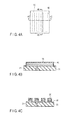
- FIG. 7A is a view schematically illustrating a distribution of impurity concentrations of first and second regions of a graphene layer along a longitudinal direction thereof.
- FIG. 7B is a view schematically illustrating a distribution of impurity concentration of the first region of the graphene layer in a width direction thereof.
- FIG. 7C is a view schematically illustrating a distribution of impurity concentrations of the second region of the graphene layer in a width direction thereof.
- FIG. 8A is a plan view illustrating a semiconductor device according to a second embodiment.
- FIG. 8B is a cross-sectional view taken along line 8 B- 8 B of FIG. 8A .
- FIG. 9A is a plan view for explaining a method of manufacturing the semiconductor device according to the second embodiment.
- FIG. 9B is a cross-sectional view taken along line 9 B- 9 B of FIG. 9A .
- FIG. 10A is a plan view for explaining the method of manufacturing the semiconductor device according to the second embodiment subsequent to FIG. 9A .
- FIG. 10B is a cross-sectional view taken along line 10 B- 10 B of FIG. 10A .
- FIG. 11A is a plan view illustrating a semiconductor device according to a third embodiment.
- FIG. 11B is a cross-sectional view taken along line 11 B- 11 B of FIG. 11A .
- FIG. 11C is a cross-sectional view taken along line 11 C- 11 C of FIG. 11A .
- FIG. 12A is a plan view for explaining a method of manufacturing the semiconductor device according to the third embodiment.
- FIG. 12B is a cross-sectional view taken along line 12 B- 1 B of FIG. 12A .
- FIG. 12C is a cross-sectional view taken along line 12 C- 12 C of FIG. 12A .
- FIG. 13A is a plan view shown for explaining the method of manufacturing the semiconductor device according to the third embodiment subsequent to FIG. 12A .
- FIG. 13B is a cross-sectional view taken along line 13 B- 13 B of FIG. 13A .
- FIG. 13C is a cross-sectional view taken along line 13 C- 13 C of FIG. 13A .
- FIG. 14A is a plan view for explaining the method of manufacturing the semiconductor device according to the third embodiment subsequent to FIG. 13A .
- FIG. 14B is a cross-sectional view taken along line 14 B- 14 B of FIG. 14A .
- FIG. 14C is a cross-sectional view taken along line 14 C- 14 C of FIG. 14A .
- FIG. 15A is a plan view for explaining the method of manufacturing the semiconductor device according to the third embodiment subsequent to FIG. 14A .
- FIG. 15B is a cross-sectional view taken along line 15 B- 15 B of FIG. 15A .
- FIG. 16A is a plan view for explaining the method of manufacturing the semiconductor device according to the third embodiment subsequent to FIG. 15A .
- FIG. 16B is a cross-sectional view taken along line 16 B- 16 B of FIG. 16A .
- FIG. 16C is a cross-sectional view taken along line 16 C- 16 C of FIG. 16A .
- a semiconductor device in general, according to one embodiment, includes a graphene layer containing impurities, and including a first region and a second region.
- the second region has a resistance higher than a resistance of the first region.
- the second region includes a side surface of an end of the graphene layer.
- the device further includes a first plug being in contact with the first region.
- a method of manufacturing a semiconductor device includes forming a first plug; forming a graphene layer being in contact with the first plug; forming a film covering an upper surface and a side surface of the graphene layer.
- the method further includes exposing a side surface of an end of the graphene layer by etching the film and the graphene layer; and forming a first region and a second region having a resistance higher than a resistance of the first region in the graphene layer by introducing impurities into the graphene layer through the exposed side surface.
- the first plug is in contact with the first region.
- FIG. 1A is a plan view illustrating a semiconductor device according to a first embodiment.
- FIG. 1B and FIG. 1C show cross-sectional views taken along lines 1 B- 1 B and 1 C- 1 C of FIG. 1A , respectively.
- 10 denotes a substrate, and an interlayer insulating film 20 is provided on the substrate 10 .
- the substrate 10 includes, for example, a semiconductor substrate such as a silicon substrate. Elements such as MOS transistors or capacitors are formed on the semiconductor substrate.
- a contact plug (a first plug) 21 connected to the substrate 10 is provided in the interlayer insulating film 20 .
- the lower surface of the first plug 21 is connected to, for example, the source region or the drain region of the MOS transistor (not shown) or an interconnect (not shown) in the substrate 10 .
- a plurality of linear graphene layers 30 constituting interconnects are provided on the interlayer insulating film 20 .
- Each graphene layer 30 contains impurities.
- the interconnects are, for example, interconnects in a memory or a logic circuit.
- FIG. 1A and FIG. 1C illustrate four graphene layers 30 .
- the number of graphene layers 30 is not limited to four.
- the shape of each graphene layer 30 is not limited to the linear shape.
- graphene includes at least one of a single-layer graphene and a stacked layer of single-layer graphenes (stacked graphene) in the present specification.
- a graphene layer is a layer including graphene.
- the graphene layer 30 includes a first region 31 and a second region 32 .
- the first region 31 is adjacent to the second region 32 .
- the second region 32 includes a side surface S 1 of one end of the graphene layer 30 .
- the second region 32 has a resistance higher than that of the first region 31 .
- An impurity concentration of the second region 32 is lower than that in the first region 31 .
- the first plug 21 is disposed under the first region 31 of the graphene layer 30 .
- An upper surface of the first plug 21 is in contact with a lower surface of the first region 31 . That is, the upper surface of the first plug 21 is in contact with the first region 31 where is a low resistance region of the lower surface of the graphene layer 30 . More specifically, the upper surface of the first plug 21 is in contact with the first region 31 without being in contact with the second region 32 having a high resistance. Thus, increase in contact resistance between the first plug 21 and the graphene layer 30 is effectively prevented.
- the upper surface of the first plug 21 is directly in contact with the lower surface of the first region 31 .
- a passivation film (a first film) 40 is provided on the upper surface and the side surface of the graphene layer 30 . As shown in FIG. 1B , the passivation film 40 covers the graphene layer 30 such that the side surface S 1 of the one end of the graphene layer 30 is exposed.
- An interlayer insulating film (a second film) 41 is provided on the passivation film 40 . As shown in FIG. 1B , the interlayer insulating film 41 covers the side surface S 1 of the one end of the graphene layer 30 .
- a via plug (a second plug) 42 connected to the graphene layer 30 is provided in the interlayer insulating film 41 and the passivation film 40 .
- the second plug 42 is disposed on the upper surface of the first region 31 .
- the lower surface of the second plug 42 is in contact with the upper surface of the first region 31 . That is, the lower surface of the second plug 42 is in contact with the first region 31 where is a low resistance region of the upper surface of the graphene layer 30 . More specifically, the lower surface of the second plug 42 is in contact with the upper surface of the first region 31 without being in contact with the second region 32 having a high resistance. Thus, increase in contact resistance between the second plug 42 and the graphene layer 30 is effectively prevented. In the present embodiment, the second plug 42 is directly in contact with the first region 31 .
- FIG. 2A , FIG. 2B and FIG. 2C [ FIG. 2A , FIG. 2B and FIG. 2C ]
- the interlayer insulating film 20 is formed on the substrate 10 . Subsequently, the first plug 21 is formed. The first plug 21 penetrates the interlayer insulating film 20 and is connected to the substrate 10 .
- the interlayer insulating film 20 is, for example, a silicon dioxide film or a silicon nitride film.
- a process for forming the first plug 21 includes, for example, forming a connection hole (not shown) which reaches the surface of the substrate 10 in the interlayer insulating film 20 by using photolithography process and etching process, forming a conductive film on the interlayer insulating film 20 in order to fill the connection hole, and removing the conductive film outside the connection hole and planarizing the surface by chemical mechanical polishing (CMP) process.
- CMP chemical mechanical polishing
- the graphene layer 30 is formed on the interlayer insulating film 20 and the first plug 21 .
- the graphene layer 30 is formed by, for example, low temperature CVD process using a source gas including carbons. It is noted that the substrate 10 is omitted in the following figures.
- FIG. 3A , FIG. 3B and FIG. 3C [ FIG. 3A , FIG. 3B and FIG. 3C ]
- a hard mask 35 is formed on the graphene layer 30 .
- the hard mask 35 has a pattern corresponding to the interconnect (graphene interconnect) to be formed.
- a thickness of the hard mask 35 is, for example, less than or equal to 100 nm.
- a process for forming the hard mask 35 includes, for example, forming a film of single-layer or multi-layer containing at least one of oxide, nitride and metal, and processing the film by using photolithography process and etching process.
- the oxide is for example SiO 2
- the nitride is for example Si 3 N 4
- the metal is W.
- the film is formed by using, for example, CVD process or PVD process.
- the graphene layer 30 is processed by etching using the hard mask 35 as a mask, thereby dividing the graphene layer 30 into a plurality of linear layers.
- each of the linear layers is also mentioned as the graphene layer 30 .
- FIG. 4A , FIG. 4B and FIG. 4C [ FIG. 4A , FIG. 4B and FIG. 4C ]
- the hard mask 35 shown in FIG. 3A to FIG. 3C is removed. Subsequently, the interlayer insulating film. 20 and the graphene layer 30 are cleaned by using wet process.
- the passivation film 40 is formed on the interlayer insulating film 20 and the graphene layer 30 .
- the passivation film 40 covers the upper surface and the side surfaces of the graphene layer 30 .
- the passivation film 40 contains, for example, a nitride such as a silicon nitride or a titanium nitride.
- the passivation film 40 is formed by, for example, ALD process or CVD process.
- FIG. 5A , FIG. 5B and FIG. 5C [ FIG. 5A , FIG. 5B and FIG. 5C ]
- the side surface S 1 of the one end of the graphene layer 30 is exposed by etching the passivation film 40 and graphene layer 30 using a resist pattern (not shown) as a mask.
- the passivation film. 40 covers the side surfaces except the side surface S 1 of the graphene layer 30 , and the upper surface of the graphene layer 30 .
- the interlayer insulating film 20 and the plug 21 cover the lower surface of the graphene layer 30 .
- the surface of the graphene layer 30 except the side surface S 1 is not exposed excluding side surface S 1 .
- the interlayer insulating film 20 , the graphene layer 30 and the passivation film. 40 are cleaned by wet process.
- FIG. 6A , FIG. 6B and FIG. 6C [ FIG. 6A , FIG. 6B and FIG. 6C ]
- the first region 31 and the second region 32 are formed in the graphene layer 30 by introducing impurities into the graphene layer 30 through the exposed side surface S 1 of the graphene 30 .
- a method for introducing the impurities into the graphene layer is, for example, a method using vaporized impurities heated in a range form 100° C. to 700° C. (intercalation), or a method using liquid impurities.
- the impurities can be introduced into the graphene layer 30 by applying a voltage to the graphene layer 30 .
- the impurities to be introduced into the graphene layer 30 include, for example, at least one of Li, Na, K, Cs, Ca, Sr, Ba, Sm, Eu, Yb, Tm, F 2 , Br 2 , ICl, IBr, MgCl 2 , AlCl 3 , FeCl 3 , CuCl 2 , SbCl 5 , MoCl 5 , AsF 5 , SbF 5 , NbF 5 , HNO 5 , H 2 SO 4 , H 3 PO 4 and HF.
- Li, Na, K, Cs, Ca, Sr, Ba, Sm, Eu, Yb and Tm are donor-type impurities
- the reset substances are acceptor-type impurities.
- the length L of the second region 32 is greater than or equal to a certain value (for example, 10 ⁇ m). In other words, in the present embodiment, the length L is a distance from the one end of the graphene layer 30 on the side surface S 1 side to the first region 31 .
- the first region 31 is longer than the second region 32 .
- the length of the first region 31 is, for example, in a rage from a few 100 ⁇ m to a few mm.
- FIG. 7A a view schematically illustrating a distribution of impurity concentrations (doping concentration [cm ⁇ 3 ]) of the first region 31 and the second region 32 of the graphene layer 30 in a longitudinal direction thereof.
- FIG. 7A shows that the impurity concentration of the second region 32 is lower than the impurity concentration of the first region 31 .
- the impurity concentration of the second region 32 increases from side surface S 1 toward the first region 31 .
- the distribution of the impurity concentration of the first region 31 has the minimum impurity concentration greater than or equal to a certain value (Nc).
- the distribution of the impurity concentration of the first region 31 has the maximum impurity concentration greater than the certain value (Nc).
- both the minimum value and the maximum value may be the certain value (Nc).
- the distribution of impurity concentration of the second region 32 has the minimum impurity concentration less than the certain value (Nc).
- the impurity concentration of the second region 32 is lower than the impurity concentration of the first region 31 , and the impurity concentration of the second region 32 increases from side surface S 1 toward the first region 31 .
- the first region 31 is a region (a high concentration region) in which the impurity concentration is greater than or equal to Nc in the entire part.
- the second region 32 is a region (a low concentration region) in which the impurity concentration is less than Nc in substantially the entire part.
- the side surface S 1 of the graphene layer 30 is a surface (an inlet) for introducing impurities into the graphene layer 30 , and is also a surface (an outlet) for discharging the impurities introduced into the graphene layer 30 .
- the impurities in a region of which the distance from the side surface S 1 is less than a constant value (a region with an unstable impurity concentration) are easily discharged through the side surface S 1 , and as for the impurities in the region, the closer the region to the side surface S 1 , the more easily the impurities is discharged through side surface S 1 .
- the impurities in a region of which the distance from the side surface S 1 is greater than or equal to the certain value (a region with a stable impurity concentration) are difficult to be discharged through side surface S 1 .
- the region with the stable impurity concentration (high concentrations region) and the region with the unstable impurity concentration (low concentration region) are different in a resistance value defined by sheet resistance, resistivity or the like.
- the difference in the resistance can be measured by using, for example, a nanoprober.
- the two regions can be distinguished by evaluating a degree of incursion of the impurities between the graphene layers at macro level by Raman spectroscopic analysis or the like.
- the distance L is not less than about 10 ⁇ m. Therefore, in the present embodiment, the distance L is ⁇ 10 ⁇ m.
- the first region 31 and the second region 32 are a high concentration region (in other words, a low resistance region) and a low concentration region (in other words, a high resistance region), respectively, and the first plug 21 is in contact with the first region 31 without being in contact with the second region.
- the increase in contact resistance between the first plug 21 and the graphene layer 30 is effectively prevented.
- FIG. 7B is a vies schematically illustrating a distribution of the impurity concentration of the first region 31 of the graphene layer 30 in a width direction.
- the impurity concentration of the first region 31 in the width direction is nearly constant value that is greater than or equal to the certain value (Nc).
- FIG. 7C is a view schematically illustrating a distribution of the impurity concentration of the second region 32 of the graphene layer 30 in a width direction.
- the impurity concentration of the second region 32 in the width direction is nearly constant value that is less than the certain value (Nc). In general, the impurity concentration of the second region 32 in the width direction decreases toward side surface S 1 .
- the distributions of the impurity concentrations shown in FIG. 7A , FIG. 7B and FIG. 7C are confirmed in a plurality of graphene layers 30 ( 30 , 31 ).
- the interlayer insulating film 41 is formed on the interlayer insulating film 20 and the passivation film. 40 such that the side surface S 1 is covered by the interlayer insulating film 41 .
- the interlayer insulating film 41 contains an oxide or a nitride.
- the interlayer insulating film 41 is formed by using, for example, CVD process, PVD process or ALD process. Subsequently, a connection hole reaching the first region 31 is formed in the interlayer insulating film 41 and the passivation film 40 , then the second plug 42 is formed in the connection hole, thereby obtaining the semiconductor device shown in FIG. 1A to FIG. 1C .
- the second plug 42 is in contact with the first region 31 (the high concentration region or the low resistance region) without being in contact with the second region 32 (the low concentration region or the high resistance region), so that the increase in contact resistance between the second plug 42 and the graphene layer 30 is effectively prevented.
- FIG. 8A is a plan view illustrating a semiconductor device according to a second embodiment.
- FIG. 8B is a cross-sectional view taken along line 8 B- 8 B of FIG. 8A .
- a graphene layer 30 further includes a third region 33 .
- the third region 33 is adjacent to a first region 31 and includes a side surface S 2 of the other end of the graphene layer 30 .
- the third region 33 has a resistance higher than that of the first region 31 .
- the impurity concentration of the third region 33 is lower than that of the first region 31 .
- the semiconductor device of the present embodiment will be further explained hereinafter according to its manufacturing method.
- FIG. 9A and FIG. 9B are identical to FIG. 9A and FIG. 9B ]
- the side surface S 1 of an end of the graphene layer 30 and the side surface S 2 of other end of the graphene layer 30 are exposed by etching the passivation film 40 and the grapheme layer 30 using a resist pattern (not shown) as a mask.
- the passivation film 40 covers the side surfaces of the graphene layer 30 other than the side surfaces S 1 and S 2 , and the upper surface of the graphene layer 30 , and an interlayer insulating film 20 and a plug 21 cover the lower surface of the graphene layer 30 .
- the surface of the graphene layer 30 is not exposed excluding the side surfaces S 1 and S 2 .
- the interlayer insulating film 20 , the graphene layer 30 and the passivation film 40 are rinsed by wet process.
- FIG. 10A and FIG. 10B are identical to FIG. 10A and FIG. 10B ]
- the first region 31 , the second region 32 and the third region are formed in the graphene layer 30 by introducing the impurities into the graphene layer 30 through the exposed side surfaces S 1 and S 2 of the graphene layer 30 .
- the impurities are introduced into the graphene layer 30 through two side surfaces S 1 and S 2 , and amount of the impurities introduced into the graphene layer 30 per unit time is increased, so that the first region 31 , which is the high impurity concentration, can be formed in shorter time.
- an interlayer insulating film 41 is formed on the interlayer insulating film 20 and the passivation film 40 such that the interlayer insulating film. 41 covers the side surfaces S 1 and S 2 , then a connection hole reaching the first region is formed in the interlayer insulating film. 20 and the passivation film 40 , and the second plug 42 is formed in the connection hole, thereby obtaining the semiconductor device shown in FIG. 8A and FIG. 8B .
- FIG. 11A is a plan view illustrating a semiconductor device according to a third embodiment.
- FIG. 11B and FIG. 11C show cross-sectional views taken along lines 11 B- 11 B and 11 C- 11 C of FIG. 11A , respectively.
- the present embodiment is different from the first embodiment in that the present embodiment further comprises a catalyst underlayer 22 and a catalyst layer 23 provided under the graphene layer 30 , and a hard mask 35 provide on the graphene layer 30 . That is, the multilayer structure including the catalyst underlayer 22 , the catalyst layer 23 , the graphene layer 30 and the hard mask 35 is used as an interconnect structure. In addition, air gap 60 is provided between the adjacent two multilayer interconnect structures.
- the semiconductor device of the present embodiment will be further explained hereinafter according to its manufacturing method.
- FIG. 12A , FIG. 12B and FIG. 12C [ FIG. 12A , FIG. 12B and FIG. 12C ]
- An interlayer insulating film 20 is formed on a substrate (not shown). Subsequently, a first plug 21 is formed, which penetrates through the interlayer insulating film 20 and is connected to the substrate.
- the catalytic underlayer 22 is formed on the interlayer insulating film. 20 and the first plug 21 .
- the material of the catalytic underlayer 22 is, for example, Ta, Ti, Ru, W, Al, a nitride of these elements or an oxide of these elements.
- the catalytic underlayer 22 has a thickness of, for example, 50 nm or less. The catalytic underlayer 22 may be omitted.
- the catalytic layer 23 is formed on the catalytic underlayer 22 .
- the catalytic layer 23 is connected to the first plug 21 via the catalytic underlayer 22 .
- the material of the catalytic layer 23 is, for example, Co, Ni, Fe, Cu, Ru, an alloy of these elements or a carbide of these elements.
- the catalytic layer 23 has a thickness of, for example, 100 nm or less.
- FIG. 13A , FIG. 13B and FIG. 13C [ FIG. 13A , FIG. 13B and FIG. 13C ]
- the graphene layer 30 is formed on the catalytic layer 23 , then the hard mask 35 is formed on the graphene layer 30 , and the stacked body of the graphene layer 30 , the catalytic layer 23 and the catalytic underlayer 22 is processed by using the hard mask 35 as a mask, thereby dividing the stacked body into a plurality of linear stacked bodies.
- FIG. 14A , FIG. 14B and FIG. 14C [ FIG. 14A , FIG. 14B and FIG. 14C ]
- a passivation film 40 is formed on the interlayer insulating film 20 , the catalytic underlayer 22 , the catalytic layer 23 , the graphene layer 30 and the hard mask 35 .
- the passivation film 40 covers the side surfaces of the catalytic underlayer 22 , the catalytic layer 23 and the graphene layer 30 , and the side surfaces and the upper surface of the hard mask 35 .
- the distance D between interconnect structures covered by the passivation film 40 is set to 30 nm or less, preferably, 10 nm or less, such that the air gap between two adjacent graphene layers 30 after an interlayer insulating film 41 is formed. If the distance D is less than or equal to a certain value, a source gas is not sufficiently supplied in a space between the interconnect structures, and the space is not filled with the interlayer insulating film 41 .
- the distance D can be controlled by the distance between the interconnect structures and the thickness of the passivation film 40 .
- FIG. 15A and FIG. 15B are identical to FIG. 15A and FIG. 15B ]
- the side surface S 1 of the end of the graphene layer 30 is exposed by etching the passivation film 40 , the hard mask 35 , the graphene layer 30 , the catalyst layer 23 and catalyst underlayer 22 using a resist pattern (not shown) as a mask.
- a resist pattern not shown
- the side surfaces of the end of the hard mask 35 , the catalyst layer 23 and the catalyst underlayer 22 are also exposed.
- FIG. 16A , FIG. 16B and FIG. 16C [ FIG. 16A , FIG. 16B and FIG. 16C ]
- the first region 31 and the second region 32 are formed in the graphene layer 30 by introducing the impurities into the graphene layer 30 through the exposed surface S 1 of the graphene layer 30 .
- the first plug 21 is indirectly in contact with the first region 31 via the catalytic underlayer 22 and the catalytic layer 23 .
- the interlayer insulating film 41 and the air gap 60 are formed, subsequently, a connection hole reaching the first region 31 is formed in the interlayer insulating film 41 and the passivation film 40 , and the second plug 42 is formed in the connection hole, thereby obtaining the semiconductor device shown in FIG. 11A to FIG. 11B .
- the interlayer insulating film may be formed between adjacent two hard masks 35 . Because the effect of the air gap is to reduce capacitance between the interconnect structures (graphene layers).
- the interlayer insulating film 41 may be formed in a manner to fill the interconnect structures as in the first embodiment. In this case, it is better to remove the hard mask 35 than to leave the hard mask 35 . Because an aspect ratio between the interconnect structures is reduced, and adequate source gas is easily supplied between the interconnect structures.
- the graphene layer 30 may further include the third region 33 as in the second embodiment.
Landscapes
- Internal Circuitry In Semiconductor Integrated Circuit Devices (AREA)
Abstract
Description
Claims (14)
Applications Claiming Priority (2)
| Application Number | Priority Date | Filing Date | Title |
|---|---|---|---|
| JP2015166690A JP6542072B2 (en) | 2015-08-26 | 2015-08-26 | Semiconductor device and method of manufacturing the same |
| JP2015-166690 | 2015-08-26 |
Publications (2)
| Publication Number | Publication Date |
|---|---|
| US20170062346A1 US20170062346A1 (en) | 2017-03-02 |
| US9865547B2 true US9865547B2 (en) | 2018-01-09 |
Family
ID=58095741
Family Applications (1)
| Application Number | Title | Priority Date | Filing Date |
|---|---|---|---|
| US15/068,506 Active US9865547B2 (en) | 2015-08-26 | 2016-03-11 | Semiconductor device and manufacturing method thereof |
Country Status (2)
| Country | Link |
|---|---|
| US (1) | US9865547B2 (en) |
| JP (1) | JP6542072B2 (en) |
Families Citing this family (3)
| Publication number | Priority date | Publication date | Assignee | Title |
|---|---|---|---|---|
| JP7002850B2 (en) * | 2017-03-22 | 2022-02-04 | 株式会社東芝 | Graphene wiring structure manufacturing method, wiring structure manufacturing method |
| US11640940B2 (en) * | 2021-05-07 | 2023-05-02 | Taiwan Semiconductor Manufacturing Company, Ltd. | Methods of forming interconnection structure including conductive graphene layers |
| US20240088042A1 (en) * | 2022-09-08 | 2024-03-14 | Taiwan Semiconductor Manufacturing Company Ltd. | Semiconductor structures and manufacturing method thereof |
Citations (8)
| Publication number | Priority date | Publication date | Assignee | Title |
|---|---|---|---|---|
| US20130099205A1 (en) * | 2011-10-21 | 2013-04-25 | University Of Utah Research Foundation | Homogeneous multiple band gap devices |
| US20140162464A1 (en) * | 2012-12-12 | 2014-06-12 | International Business Machines Corporation | Authentication using graphene based devices as physical unclonable functions |
| US20140231751A1 (en) | 2013-02-15 | 2014-08-21 | Kabushiki Kaisha Toshiba | Semiconductor device |
| US20140284798A1 (en) | 2013-03-19 | 2014-09-25 | Kabushiki Kaisha Toshiba | Graphene wiring and method of manufacturing the same |
| US20140319685A1 (en) * | 2013-04-30 | 2014-10-30 | International Business Machines Corporation | Hybrid Graphene-Metal Interconnect Structures |
| US20150061133A1 (en) | 2013-08-30 | 2015-03-05 | Kabushiki Kaisha Toshiba | Semiconductor device and manufacturing method of the same |
| JP2015061042A (en) | 2013-09-20 | 2015-03-30 | 独立行政法人産業技術総合研究所 | Method for manufacturing wiring structure, and wiring structure |
| US20150137377A1 (en) * | 2012-12-17 | 2015-05-21 | International Business Machines Corporation | Graphene and metal interconnects with reduced contact resistance |
Family Cites Families (3)
| Publication number | Priority date | Publication date | Assignee | Title |
|---|---|---|---|---|
| US6787122B2 (en) * | 2001-06-18 | 2004-09-07 | The University Of North Carolina At Chapel Hill | Method of making nanotube-based material with enhanced electron field emission properties |
| JP5583236B1 (en) * | 2013-03-19 | 2014-09-03 | 株式会社東芝 | Graphene wiring |
| JP2016174039A (en) * | 2015-03-16 | 2016-09-29 | 株式会社東芝 | Semiconductor device and manufacturing method of semiconductor device |
-
2015
- 2015-08-26 JP JP2015166690A patent/JP6542072B2/en active Active
-
2016
- 2016-03-11 US US15/068,506 patent/US9865547B2/en active Active
Patent Citations (8)
| Publication number | Priority date | Publication date | Assignee | Title |
|---|---|---|---|---|
| US20130099205A1 (en) * | 2011-10-21 | 2013-04-25 | University Of Utah Research Foundation | Homogeneous multiple band gap devices |
| US20140162464A1 (en) * | 2012-12-12 | 2014-06-12 | International Business Machines Corporation | Authentication using graphene based devices as physical unclonable functions |
| US20150137377A1 (en) * | 2012-12-17 | 2015-05-21 | International Business Machines Corporation | Graphene and metal interconnects with reduced contact resistance |
| US20140231751A1 (en) | 2013-02-15 | 2014-08-21 | Kabushiki Kaisha Toshiba | Semiconductor device |
| US20140284798A1 (en) | 2013-03-19 | 2014-09-25 | Kabushiki Kaisha Toshiba | Graphene wiring and method of manufacturing the same |
| US20140319685A1 (en) * | 2013-04-30 | 2014-10-30 | International Business Machines Corporation | Hybrid Graphene-Metal Interconnect Structures |
| US20150061133A1 (en) | 2013-08-30 | 2015-03-05 | Kabushiki Kaisha Toshiba | Semiconductor device and manufacturing method of the same |
| JP2015061042A (en) | 2013-09-20 | 2015-03-30 | 独立行政法人産業技術総合研究所 | Method for manufacturing wiring structure, and wiring structure |
Non-Patent Citations (3)
| Title |
|---|
| Azad Naeemi, et al., "Conductance Modeling for Graphene Nanoribbon (GNR) Interconnects", IEEE Electron Device Letters, vol. 28, No. 5, May 2007, pp. 428-431. |
| Azad Naeemi, et al., "Performance Benchmarking for Graphene Nanoribbon, Carbon Nanotube, and Cu Interconnects", Interconnect Technology Conference, Jun. 1-4, 2008, pp. 183-185. |
| Chuan Xu, et al., "Graphene Nano-Ribbon (GNR) Interconnects: A Genuine Contender or a Delusive Dream?", Electron Devices Meeting, Dec. 15-17, 2008, pp. 201-204. |
Also Published As
| Publication number | Publication date |
|---|---|
| US20170062346A1 (en) | 2017-03-02 |
| JP6542072B2 (en) | 2019-07-10 |
| JP2017045833A (en) | 2017-03-02 |
Similar Documents
| Publication | Publication Date | Title |
|---|---|---|
| US8357609B2 (en) | Dual damascene-like subtractive metal etch scheme | |
| TWI401745B (en) | Semiconductor device and manufacturing method thereof | |
| JP5820416B2 (en) | Semiconductor device and manufacturing method thereof | |
| US9112146B2 (en) | Resistance random access memory device | |
| US9478584B2 (en) | Nonvolatile memory device and method for manufacturing the same | |
| CN107452714B (en) | Apparatus and method for forming low resistivity noble metal interconnects | |
| JP7706860B2 (en) | Topological semimetallic interconnects | |
| US20150228531A1 (en) | Integrated circuit device and method for manufacturing same | |
| CN105493244A (en) | Methods of forming parallel wires of different metal materials through double patterning and fill techniques | |
| US20190096751A1 (en) | Dual Damascene Process for Forming Vias and Interconnects in an Integrated Circuit Structure | |
| US9865547B2 (en) | Semiconductor device and manufacturing method thereof | |
| TWI469257B (en) | Method of forming a semiconductor device having a capacitor and via contact | |
| US20090206491A1 (en) | Semiconductor device | |
| Lo et al. | BEOL compatible sub-nm diffusion barrier for advanced Cu interconnects | |
| JP2023168319A (en) | Resistive Random Access Memory with Post-Patterned Memory Film to Provide Improved Durability Properties and Method of Forming the Same | |
| US10128184B2 (en) | Antifuse structure in via hole in interplayer dielectric | |
| US9484206B2 (en) | Semiconductor device including catalyst layer and graphene layer thereon and method for manufacturing the same | |
| JP2013105891A (en) | Semiconductor device and manufacturing method of the same | |
| JP2009200256A (en) | Method of manufacturing semiconductor device | |
| US9852987B2 (en) | Semiconductor device and method of manufacturing the same | |
| JP4342226B2 (en) | Semiconductor device and manufacturing method thereof | |
| JP6197381B2 (en) | Semiconductor device and manufacturing method thereof | |
| US9761531B2 (en) | Semiconductor device and method of manufacturing the same | |
| JP6123501B2 (en) | Semiconductor device and manufacturing method thereof | |
| US12057445B2 (en) | Method of manufacturing a semiconductor device and a semiconductor device |
Legal Events
| Date | Code | Title | Description |
|---|---|---|---|
| AS | Assignment |
Owner name: KABUSHIKI KAISHA TOSHIBA, JAPAN Free format text: ASSIGNMENT OF ASSIGNORS INTEREST;ASSIGNORS:ISOBAYASHI, ATSUNOBU;KAJITA, AKIHIRO;SAKAI, TADASHI;REEL/FRAME:038223/0918 Effective date: 20160325 |
|
| STCF | Information on status: patent grant |
Free format text: PATENTED CASE |
|
| AS | Assignment |
Owner name: TOSHIBA MEMORY CORPORATION, JAPAN Free format text: DE-MERGER;ASSIGNOR:KABUSHIKI KAISHA TOSHIBA;REEL/FRAME:051260/0291 Effective date: 20170401 Owner name: TOSHIBA MEMORY CORPORATION, JAPAN Free format text: MERGER;ASSIGNORS:TOSHIBA MEMORY CORPORATION;K.K PANGEA;REEL/FRAME:051262/0776 Effective date: 20180801 Owner name: KIOXIA CORPORATION, JAPAN Free format text: CHANGE OF NAME AND ADDRESS;ASSIGNOR:TOSHIBA MEMORY CORPORATION;REEL/FRAME:051262/0881 Effective date: 20191001 |
|
| MAFP | Maintenance fee payment |
Free format text: PAYMENT OF MAINTENANCE FEE, 4TH YEAR, LARGE ENTITY (ORIGINAL EVENT CODE: M1551); ENTITY STATUS OF PATENT OWNER: LARGE ENTITY Year of fee payment: 4 |
|
| MAFP | Maintenance fee payment |
Free format text: PAYMENT OF MAINTENANCE FEE, 8TH YEAR, LARGE ENTITY (ORIGINAL EVENT CODE: M1552); ENTITY STATUS OF PATENT OWNER: LARGE ENTITY Year of fee payment: 8 |