US9859397B2 - Growing groups III-V lateral nanowire channels - Google Patents
Growing groups III-V lateral nanowire channels Download PDFInfo
- Publication number
- US9859397B2 US9859397B2 US15/585,231 US201715585231A US9859397B2 US 9859397 B2 US9859397 B2 US 9859397B2 US 201715585231 A US201715585231 A US 201715585231A US 9859397 B2 US9859397 B2 US 9859397B2
- Authority
- US
- United States
- Prior art keywords
- silicon
- nanowire
- mandrel
- directly
- layer
- Prior art date
- Legal status (The legal status is an assumption and is not a legal conclusion. Google has not performed a legal analysis and makes no representation as to the accuracy of the status listed.)
- Expired - Fee Related
Links
Images


Classifications
-
- H01L29/66522—
-
- H—ELECTRICITY
- H10—SEMICONDUCTOR DEVICES; ELECTRIC SOLID-STATE DEVICES NOT OTHERWISE PROVIDED FOR
- H10D—INORGANIC ELECTRIC SEMICONDUCTOR DEVICES
- H10D30/00—Field-effect transistors [FET]
- H10D30/01—Manufacture or treatment
- H10D30/021—Manufacture or treatment of FETs having insulated gates [IGFET]
-
- B—PERFORMING OPERATIONS; TRANSPORTING
- B82—NANOTECHNOLOGY
- B82Y—SPECIFIC USES OR APPLICATIONS OF NANOSTRUCTURES; MEASUREMENT OR ANALYSIS OF NANOSTRUCTURES; MANUFACTURE OR TREATMENT OF NANOSTRUCTURES
- B82Y10/00—Nanotechnology for information processing, storage or transmission, e.g. quantum computing or single electron logic
-
- H01L21/02381—
-
- H01L21/0242—
-
- H01L21/02422—
-
- H01L21/02433—
-
- H01L21/0245—
-
- H01L21/02488—
-
- H01L21/02502—
-
- H01L21/02538—
-
- H01L21/02603—
-
- H01L21/02639—
-
- H01L21/02645—
-
- H01L21/26546—
-
- H01L21/30604—
-
- H01L21/30612—
-
- H01L21/30617—
-
- H01L21/3086—
-
- H01L21/7624—
-
- H01L29/045—
-
- H01L29/0673—
-
- H01L29/20—
-
- H01L29/42392—
-
- H01L29/78681—
-
- H—ELECTRICITY
- H10—SEMICONDUCTOR DEVICES; ELECTRIC SOLID-STATE DEVICES NOT OTHERWISE PROVIDED FOR
- H10D—INORGANIC ELECTRIC SEMICONDUCTOR DEVICES
- H10D30/00—Field-effect transistors [FET]
- H10D30/01—Manufacture or treatment
- H10D30/014—Manufacture or treatment of FETs having zero-dimensional [0D] or one-dimensional [1D] channels, e.g. quantum wire FETs, single-electron transistors [SET] or Coulomb blockade transistors
-
- H—ELECTRICITY
- H10—SEMICONDUCTOR DEVICES; ELECTRIC SOLID-STATE DEVICES NOT OTHERWISE PROVIDED FOR
- H10D—INORGANIC ELECTRIC SEMICONDUCTOR DEVICES
- H10D30/00—Field-effect transistors [FET]
- H10D30/40—FETs having zero-dimensional [0D], one-dimensional [1D] or two-dimensional [2D] charge carrier gas channels
- H10D30/43—FETs having zero-dimensional [0D], one-dimensional [1D] or two-dimensional [2D] charge carrier gas channels having one-dimensional [1D] charge carrier gas channels, e.g. quantum wire FETs or transistors having 1D quantum-confined channels
-
- H—ELECTRICITY
- H10—SEMICONDUCTOR DEVICES; ELECTRIC SOLID-STATE DEVICES NOT OTHERWISE PROVIDED FOR
- H10D—INORGANIC ELECTRIC SEMICONDUCTOR DEVICES
- H10D30/00—Field-effect transistors [FET]
- H10D30/60—Insulated-gate field-effect transistors [IGFET]
- H10D30/62—Fin field-effect transistors [FinFET]
- H10D30/6212—Fin field-effect transistors [FinFET] having fin-shaped semiconductor bodies having non-rectangular cross-sections
-
- H—ELECTRICITY
- H10—SEMICONDUCTOR DEVICES; ELECTRIC SOLID-STATE DEVICES NOT OTHERWISE PROVIDED FOR
- H10D—INORGANIC ELECTRIC SEMICONDUCTOR DEVICES
- H10D30/00—Field-effect transistors [FET]
- H10D30/60—Insulated-gate field-effect transistors [IGFET]
- H10D30/67—Thin-film transistors [TFT]
- H10D30/6729—Thin-film transistors [TFT] characterised by the electrodes
- H10D30/673—Thin-film transistors [TFT] characterised by the electrodes characterised by the shapes, relative sizes or dispositions of the gate electrodes
- H10D30/6735—Thin-film transistors [TFT] characterised by the electrodes characterised by the shapes, relative sizes or dispositions of the gate electrodes having gates fully surrounding the channels, e.g. gate-all-around
-
- H—ELECTRICITY
- H10—SEMICONDUCTOR DEVICES; ELECTRIC SOLID-STATE DEVICES NOT OTHERWISE PROVIDED FOR
- H10D—INORGANIC ELECTRIC SEMICONDUCTOR DEVICES
- H10D30/00—Field-effect transistors [FET]
- H10D30/60—Insulated-gate field-effect transistors [IGFET]
- H10D30/67—Thin-film transistors [TFT]
- H10D30/674—Thin-film transistors [TFT] characterised by the active materials
- H10D30/675—Group III-V materials, Group II-VI materials, Group IV-VI materials, selenium or tellurium
-
- H—ELECTRICITY
- H10—SEMICONDUCTOR DEVICES; ELECTRIC SOLID-STATE DEVICES NOT OTHERWISE PROVIDED FOR
- H10D—INORGANIC ELECTRIC SEMICONDUCTOR DEVICES
- H10D30/00—Field-effect transistors [FET]
- H10D30/60—Insulated-gate field-effect transistors [IGFET]
- H10D30/67—Thin-film transistors [TFT]
- H10D30/6757—Thin-film transistors [TFT] characterised by the structure of the channel, e.g. transverse or longitudinal shape or doping profile
-
- H—ELECTRICITY
- H10—SEMICONDUCTOR DEVICES; ELECTRIC SOLID-STATE DEVICES NOT OTHERWISE PROVIDED FOR
- H10D—INORGANIC ELECTRIC SEMICONDUCTOR DEVICES
- H10D62/00—Semiconductor bodies, or regions thereof, of devices having potential barriers
- H10D62/10—Shapes, relative sizes or dispositions of the regions of the semiconductor bodies; Shapes of the semiconductor bodies
- H10D62/117—Shapes of semiconductor bodies
- H10D62/118—Nanostructure semiconductor bodies
- H10D62/119—Nanowire, nanosheet or nanotube semiconductor bodies
- H10D62/121—Nanowire, nanosheet or nanotube semiconductor bodies oriented parallel to substrates
-
- H—ELECTRICITY
- H10—SEMICONDUCTOR DEVICES; ELECTRIC SOLID-STATE DEVICES NOT OTHERWISE PROVIDED FOR
- H10D—INORGANIC ELECTRIC SEMICONDUCTOR DEVICES
- H10D62/00—Semiconductor bodies, or regions thereof, of devices having potential barriers
- H10D62/10—Shapes, relative sizes or dispositions of the regions of the semiconductor bodies; Shapes of the semiconductor bodies
- H10D62/13—Semiconductor regions connected to electrodes carrying current to be rectified, amplified or switched, e.g. source or drain regions
- H10D62/149—Source or drain regions of field-effect devices
- H10D62/151—Source or drain regions of field-effect devices of IGFETs
-
- H—ELECTRICITY
- H10—SEMICONDUCTOR DEVICES; ELECTRIC SOLID-STATE DEVICES NOT OTHERWISE PROVIDED FOR
- H10D—INORGANIC ELECTRIC SEMICONDUCTOR DEVICES
- H10D62/00—Semiconductor bodies, or regions thereof, of devices having potential barriers
- H10D62/40—Crystalline structures
- H10D62/405—Orientations of crystalline planes
-
- H—ELECTRICITY
- H10—SEMICONDUCTOR DEVICES; ELECTRIC SOLID-STATE DEVICES NOT OTHERWISE PROVIDED FOR
- H10D—INORGANIC ELECTRIC SEMICONDUCTOR DEVICES
- H10D62/00—Semiconductor bodies, or regions thereof, of devices having potential barriers
- H10D62/80—Semiconductor bodies, or regions thereof, of devices having potential barriers characterised by the materials
- H10D62/85—Semiconductor bodies, or regions thereof, of devices having potential barriers characterised by the materials being Group III-V materials, e.g. GaAs
-
- H—ELECTRICITY
- H10—SEMICONDUCTOR DEVICES; ELECTRIC SOLID-STATE DEVICES NOT OTHERWISE PROVIDED FOR
- H10P—GENERIC PROCESSES OR APPARATUS FOR THE MANUFACTURE OR TREATMENT OF DEVICES COVERED BY CLASS H10
- H10P14/00—Formation of materials, e.g. in the shape of layers or pillars
- H10P14/20—Formation of materials, e.g. in the shape of layers or pillars of semiconductor materials
- H10P14/27—Formation of materials, e.g. in the shape of layers or pillars of semiconductor materials using selective deposition, e.g. simultaneous growth of monocrystalline and non-monocrystalline semiconductor materials
- H10P14/271—Formation of materials, e.g. in the shape of layers or pillars of semiconductor materials using selective deposition, e.g. simultaneous growth of monocrystalline and non-monocrystalline semiconductor materials characterised by the preparation of substrate for selective deposition
- H10P14/274—Formation of materials, e.g. in the shape of layers or pillars of semiconductor materials using selective deposition, e.g. simultaneous growth of monocrystalline and non-monocrystalline semiconductor materials characterised by the preparation of substrate for selective deposition using seed materials
-
- H—ELECTRICITY
- H10—SEMICONDUCTOR DEVICES; ELECTRIC SOLID-STATE DEVICES NOT OTHERWISE PROVIDED FOR
- H10P—GENERIC PROCESSES OR APPARATUS FOR THE MANUFACTURE OR TREATMENT OF DEVICES COVERED BY CLASS H10
- H10P14/00—Formation of materials, e.g. in the shape of layers or pillars
- H10P14/20—Formation of materials, e.g. in the shape of layers or pillars of semiconductor materials
- H10P14/29—Formation of materials, e.g. in the shape of layers or pillars of semiconductor materials characterised by the substrates
- H10P14/2901—Materials
- H10P14/2902—Materials being Group IVA materials
- H10P14/2905—Silicon, silicon germanium or germanium
-
- H—ELECTRICITY
- H10—SEMICONDUCTOR DEVICES; ELECTRIC SOLID-STATE DEVICES NOT OTHERWISE PROVIDED FOR
- H10P—GENERIC PROCESSES OR APPARATUS FOR THE MANUFACTURE OR TREATMENT OF DEVICES COVERED BY CLASS H10
- H10P14/00—Formation of materials, e.g. in the shape of layers or pillars
- H10P14/20—Formation of materials, e.g. in the shape of layers or pillars of semiconductor materials
- H10P14/29—Formation of materials, e.g. in the shape of layers or pillars of semiconductor materials characterised by the substrates
- H10P14/2901—Materials
- H10P14/2921—Materials being crystalline insulating materials
-
- H—ELECTRICITY
- H10—SEMICONDUCTOR DEVICES; ELECTRIC SOLID-STATE DEVICES NOT OTHERWISE PROVIDED FOR
- H10P—GENERIC PROCESSES OR APPARATUS FOR THE MANUFACTURE OR TREATMENT OF DEVICES COVERED BY CLASS H10
- H10P14/00—Formation of materials, e.g. in the shape of layers or pillars
- H10P14/20—Formation of materials, e.g. in the shape of layers or pillars of semiconductor materials
- H10P14/29—Formation of materials, e.g. in the shape of layers or pillars of semiconductor materials characterised by the substrates
- H10P14/2901—Materials
- H10P14/2922—Materials being non-crystalline insulating materials, e.g. glass or polymers
-
- H—ELECTRICITY
- H10—SEMICONDUCTOR DEVICES; ELECTRIC SOLID-STATE DEVICES NOT OTHERWISE PROVIDED FOR
- H10P—GENERIC PROCESSES OR APPARATUS FOR THE MANUFACTURE OR TREATMENT OF DEVICES COVERED BY CLASS H10
- H10P14/00—Formation of materials, e.g. in the shape of layers or pillars
- H10P14/20—Formation of materials, e.g. in the shape of layers or pillars of semiconductor materials
- H10P14/29—Formation of materials, e.g. in the shape of layers or pillars of semiconductor materials characterised by the substrates
- H10P14/2926—Crystal orientations
-
- H—ELECTRICITY
- H10—SEMICONDUCTOR DEVICES; ELECTRIC SOLID-STATE DEVICES NOT OTHERWISE PROVIDED FOR
- H10P—GENERIC PROCESSES OR APPARATUS FOR THE MANUFACTURE OR TREATMENT OF DEVICES COVERED BY CLASS H10
- H10P14/00—Formation of materials, e.g. in the shape of layers or pillars
- H10P14/20—Formation of materials, e.g. in the shape of layers or pillars of semiconductor materials
- H10P14/32—Formation of materials, e.g. in the shape of layers or pillars of semiconductor materials characterised by intermediate layers between substrates and deposited layers
- H10P14/3202—Materials thereof
- H10P14/3204—Materials thereof being Group IVA semiconducting materials
- H10P14/3211—Silicon, silicon germanium or germanium
-
- H—ELECTRICITY
- H10—SEMICONDUCTOR DEVICES; ELECTRIC SOLID-STATE DEVICES NOT OTHERWISE PROVIDED FOR
- H10P—GENERIC PROCESSES OR APPARATUS FOR THE MANUFACTURE OR TREATMENT OF DEVICES COVERED BY CLASS H10
- H10P14/00—Formation of materials, e.g. in the shape of layers or pillars
- H10P14/20—Formation of materials, e.g. in the shape of layers or pillars of semiconductor materials
- H10P14/32—Formation of materials, e.g. in the shape of layers or pillars of semiconductor materials characterised by intermediate layers between substrates and deposited layers
- H10P14/3202—Materials thereof
- H10P14/3238—Materials thereof being insulating materials
-
- H—ELECTRICITY
- H10—SEMICONDUCTOR DEVICES; ELECTRIC SOLID-STATE DEVICES NOT OTHERWISE PROVIDED FOR
- H10P—GENERIC PROCESSES OR APPARATUS FOR THE MANUFACTURE OR TREATMENT OF DEVICES COVERED BY CLASS H10
- H10P14/00—Formation of materials, e.g. in the shape of layers or pillars
- H10P14/20—Formation of materials, e.g. in the shape of layers or pillars of semiconductor materials
- H10P14/32—Formation of materials, e.g. in the shape of layers or pillars of semiconductor materials characterised by intermediate layers between substrates and deposited layers
- H10P14/3242—Structure
- H10P14/3244—Layer structure
- H10P14/3248—Layer structure consisting of two layers
-
- H—ELECTRICITY
- H10—SEMICONDUCTOR DEVICES; ELECTRIC SOLID-STATE DEVICES NOT OTHERWISE PROVIDED FOR
- H10P—GENERIC PROCESSES OR APPARATUS FOR THE MANUFACTURE OR TREATMENT OF DEVICES COVERED BY CLASS H10
- H10P14/00—Formation of materials, e.g. in the shape of layers or pillars
- H10P14/20—Formation of materials, e.g. in the shape of layers or pillars of semiconductor materials
- H10P14/34—Deposited materials, e.g. layers
- H10P14/3402—Deposited materials, e.g. layers characterised by the chemical composition
- H10P14/3414—Deposited materials, e.g. layers characterised by the chemical composition being group IIIA-VIA materials
-
- H—ELECTRICITY
- H10—SEMICONDUCTOR DEVICES; ELECTRIC SOLID-STATE DEVICES NOT OTHERWISE PROVIDED FOR
- H10P—GENERIC PROCESSES OR APPARATUS FOR THE MANUFACTURE OR TREATMENT OF DEVICES COVERED BY CLASS H10
- H10P14/00—Formation of materials, e.g. in the shape of layers or pillars
- H10P14/20—Formation of materials, e.g. in the shape of layers or pillars of semiconductor materials
- H10P14/34—Deposited materials, e.g. layers
- H10P14/3451—Structure
- H10P14/3452—Microstructure
- H10P14/3462—Nanowires
-
- H—ELECTRICITY
- H10—SEMICONDUCTOR DEVICES; ELECTRIC SOLID-STATE DEVICES NOT OTHERWISE PROVIDED FOR
- H10P—GENERIC PROCESSES OR APPARATUS FOR THE MANUFACTURE OR TREATMENT OF DEVICES COVERED BY CLASS H10
- H10P30/00—Ion implantation into wafers, substrates or parts of devices
- H10P30/20—Ion implantation into wafers, substrates or parts of devices into semiconductor materials, e.g. for doping
- H10P30/202—Ion implantation into wafers, substrates or parts of devices into semiconductor materials, e.g. for doping characterised by the semiconductor materials
- H10P30/206—Ion implantation into wafers, substrates or parts of devices into semiconductor materials, e.g. for doping characterised by the semiconductor materials into Group III-V semiconductors
-
- H—ELECTRICITY
- H10—SEMICONDUCTOR DEVICES; ELECTRIC SOLID-STATE DEVICES NOT OTHERWISE PROVIDED FOR
- H10P—GENERIC PROCESSES OR APPARATUS FOR THE MANUFACTURE OR TREATMENT OF DEVICES COVERED BY CLASS H10
- H10P30/00—Ion implantation into wafers, substrates or parts of devices
- H10P30/20—Ion implantation into wafers, substrates or parts of devices into semiconductor materials, e.g. for doping
- H10P30/21—Ion implantation into wafers, substrates or parts of devices into semiconductor materials, e.g. for doping of electrically active species
-
- H—ELECTRICITY
- H10—SEMICONDUCTOR DEVICES; ELECTRIC SOLID-STATE DEVICES NOT OTHERWISE PROVIDED FOR
- H10P—GENERIC PROCESSES OR APPARATUS FOR THE MANUFACTURE OR TREATMENT OF DEVICES COVERED BY CLASS H10
- H10P50/00—Etching of wafers, substrates or parts of devices
- H10P50/60—Wet etching
- H10P50/64—Wet etching of semiconductor materials
- H10P50/642—Chemical etching
- H10P50/646—Chemical etching of Group III-V materials
- H10P50/648—Anisotropic liquid etching
-
- H—ELECTRICITY
- H10—SEMICONDUCTOR DEVICES; ELECTRIC SOLID-STATE DEVICES NOT OTHERWISE PROVIDED FOR
- H10P—GENERIC PROCESSES OR APPARATUS FOR THE MANUFACTURE OR TREATMENT OF DEVICES COVERED BY CLASS H10
- H10P50/00—Etching of wafers, substrates or parts of devices
- H10P50/69—Etching of wafers, substrates or parts of devices using masks for semiconductor materials
- H10P50/691—Etching of wafers, substrates or parts of devices using masks for semiconductor materials for Group V materials or Group III-V materials
- H10P50/693—Etching of wafers, substrates or parts of devices using masks for semiconductor materials for Group V materials or Group III-V materials characterised by their size, orientation, disposition, behaviour or shape, in horizontal or vertical plane
- H10P50/695—Etching of wafers, substrates or parts of devices using masks for semiconductor materials for Group V materials or Group III-V materials characterised by their size, orientation, disposition, behaviour or shape, in horizontal or vertical plane characterised by the process involved to create the mask, e.g. lift-off masks or sidewalls or to modify the mask
-
- H—ELECTRICITY
- H10—SEMICONDUCTOR DEVICES; ELECTRIC SOLID-STATE DEVICES NOT OTHERWISE PROVIDED FOR
- H10P—GENERIC PROCESSES OR APPARATUS FOR THE MANUFACTURE OR TREATMENT OF DEVICES COVERED BY CLASS H10
- H10P90/00—Preparation of wafers not covered by a single main group of this subclass, e.g. wafer reinforcement
- H10P90/19—Preparing inhomogeneous wafers
- H10P90/1904—Preparing vertically inhomogeneous wafers
- H10P90/1906—Preparing SOI wafers
-
- H—ELECTRICITY
- H10—SEMICONDUCTOR DEVICES; ELECTRIC SOLID-STATE DEVICES NOT OTHERWISE PROVIDED FOR
- H10W—GENERIC PACKAGES, INTERCONNECTIONS, CONNECTORS OR OTHER CONSTRUCTIONAL DETAILS OF DEVICES COVERED BY CLASS H10
- H10W10/00—Isolation regions in semiconductor bodies between components of integrated devices
- H10W10/10—Isolation regions comprising dielectric materials
- H10W10/181—Semiconductor-on-insulator [SOI] isolation regions, e.g. buried oxide regions of SOI wafers
-
- H—ELECTRICITY
- H10—SEMICONDUCTOR DEVICES; ELECTRIC SOLID-STATE DEVICES NOT OTHERWISE PROVIDED FOR
- H10D—INORGANIC ELECTRIC SEMICONDUCTOR DEVICES
- H10D84/00—Integrated devices formed in or on semiconductor substrates that comprise only semiconducting layers, e.g. on Si wafers or on GaAs-on-Si wafers
- H10D84/01—Manufacture or treatment
- H10D84/02—Manufacture or treatment characterised by using material-based technologies
- H10D84/08—Manufacture or treatment characterised by using material-based technologies using combinations of technologies, e.g. using both Si and SiC technologies or using both Si and Group III-V technologies
-
- H—ELECTRICITY
- H10—SEMICONDUCTOR DEVICES; ELECTRIC SOLID-STATE DEVICES NOT OTHERWISE PROVIDED FOR
- H10P—GENERIC PROCESSES OR APPARATUS FOR THE MANUFACTURE OR TREATMENT OF DEVICES COVERED BY CLASS H10
- H10P50/00—Etching of wafers, substrates or parts of devices
- H10P50/60—Wet etching
- H10P50/64—Wet etching of semiconductor materials
- H10P50/642—Chemical etching
- H10P50/644—Anisotropic liquid etching
-
- H—ELECTRICITY
- H10—SEMICONDUCTOR DEVICES; ELECTRIC SOLID-STATE DEVICES NOT OTHERWISE PROVIDED FOR
- H10P—GENERIC PROCESSES OR APPARATUS FOR THE MANUFACTURE OR TREATMENT OF DEVICES COVERED BY CLASS H10
- H10P50/00—Etching of wafers, substrates or parts of devices
- H10P50/69—Etching of wafers, substrates or parts of devices using masks for semiconductor materials
- H10P50/691—Etching of wafers, substrates or parts of devices using masks for semiconductor materials for Group V materials or Group III-V materials
- H10P50/693—Etching of wafers, substrates or parts of devices using masks for semiconductor materials for Group V materials or Group III-V materials characterised by their size, orientation, disposition, behaviour or shape, in horizontal or vertical plane
Definitions
- the present disclosure relates generally to semiconductor devices and relates more specifically to field effect transistors fabricated in accordance with complementary metal-oxide-semiconductor technology and including laterally grown nanowire channels.
- Groups III-V semiconductor materials have been shown to be superior to silicon for particular applications, including, for example, optoelectronic applications.
- a layer of a Group III-V material may be grown over a semiconductor substrate in a pillar shape, with a narrow diameter and a height which is sufficiently long compared the diameter.
- the resultant structure may be referred to as a “nanowire.”
- a method for fabricating a semiconductor device includes forming a mandrel comprising silicon. Sidewalls of the silicon are orientated normal to the ⁇ 111> direction of the silicon. A nanowire is grown directly on at least one of the sidewalls of the silicon and is formed from a material selected from Groups III-V. Only one end of the nanowire directly contacts the silicon.
- a method for fabricating a semiconductor device includes forming a mandrel.
- the mandrel comprises a layer of silicon and a mask layer formed directly on the layer of silicon.
- a growth mask is deposited directly on the mandrel, and a photoresist layer is deposited directly on the growth mask.
- the photoresist layer is patterned, resulting in the removal of a portion of the photoresist layer. Portions of the growth mask that resided directly beneath the removed portion of the photoresist layer are then etched to expose a portion of the sidewalls.
- a nanowire is grown directly on the portion of the sidewalls.
- the nanowire is formed from a material selected from Groups III-V, and only one end of the nanowire directly contacts the layer of silicon.
- a semiconductor device in another example, includes a mandrel comprising silicon.
- the sidewalls of the silicon are orientated normal to a ⁇ 111> direction of the silicon.
- a nanowire is grown directly on at least one of the sidewalls.
- the nanowire is formed from a material selected from Groups III-V, and only one end of the nanowire directly contacts the silicon.
- FIGS. 1A-1H illustrate a semiconductor device during various stages of a first fabrication process performed according to examples of the present disclosure
- FIGS. 2A-2D illustrate a semiconductor device during various stages of a second fabrication process performed according to examples of the present disclosure.
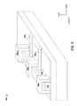
- FIG. 3 illustrates an isometric view of a semiconductor device including multiple laterally grown nanowire channels.
- CMOS complementary metal-oxide-semiconductor
- Examples of the present disclosure grow Group III-V lateral nanowire channels in a manner that is compatible with CMOS integration.
- the nanowires are grown laterally on a sidewall of a silicon mandrel. By limiting the growth area to the sidewall, nanowire channels can be formed in a manner that is easier to incorporate into existing CMOS integration schemes than vertically orientated channels.
- FIGS. 1A-1H illustrate a semiconductor device 100 during various stages of a first fabrication process performed according to examples of the present disclosure. As such, when viewed in sequence, 1 A- 1 H also serve as a flow diagram for the first fabrication process. In particular, FIGS. 1A-1H illustrate isometric views of the semiconductor device 100 during the various stages of the first fabrication process.
- one example of the semiconductor device 100 begins as a substrate 102 , formed, for example, from bulk silicon (Si).
- a buried oxide (BOX) layer 104 is formed directly on the substrate 102 .
- a silicon layer 106 is formed directly on the buried oxide layer 104 .
- the silicon layer 106 may be formed, for example, from a bulk silicon wafer or a silicon-on-insulator (SOI) wafer.
- the silicon layer 106 whether formed from bulk silicon or SOI, is a (110) silicon wafer (i.e., the wafer is flat in the ⁇ 110> direction, as illustrated by the coordinate axes).
- An etch mask 108 is formed directly on the silicon layer 106 .
- the etch mask 108 may be formed, for example, from silicon dioxide (SiO 2 ), silicon nitride (SiN x ), or aluminum oxide (Al 2 O 3 ).
- FIG. 1A illustrates the semiconductor device 100 after patterning of the etch mask 108 , which may be performed using a dry etch process and results in the removal of a portion of the etch mask 108 down to the silicon layer 106 .
- the patterning defines dimensions of at least one mandrel 110 formed partially of the etch mask material (only one mandrel 110 is illustrated in FIG. 1A for clarity).
- the mandrel 110 is orientated such that its longest dimension is parallel to the ⁇ 112> direction of the silicon layer 106 , as illustrated by the coordinate axes.
- the silicon layer 106 is next etched, for example using an anisotropic wet etch process (using, for instance, potassium hydroxide or tetramethylammonium hydroxide).
- etching of the silicon layer 106 results in the removal of any portions of the silicon layer 106 that do not reside directly beneath the etch mask 108 .
- the mandrel 110 whose dimensions were defined in FIG. 1A includes both a portion of the etch mask 108 and a portion of the silicon layer 106 .
- the silicon portion of the mandrel 110 has a vertical sidewall that is orientated in a manner that is normal to the ⁇ 111> direction of the silicon layer 106 , as illustrated by the coordinate axes.
- the vertical sidewall has an atomically flat surface due to the facet-selective nature of the etching process.
- a growth mask 112 is next deposited over the semiconductor device 100 , directly on the buried oxide layer 104 and the mandrel 110 .
- the growth mask may be formed, for example, from an oxide.
- FIG. 1D illustrates the semiconductor device 100 after patterning of the photoresist layer 114 , which results in the removal of a portion of the photoresist layer 114 down to the growth mask 112 .
- the portions of the growth mask 112 that do not reside directly beneath the photoresist layer 114 are next etched down to the buried oxide layer 104 , for example using a wet etch process. Etching of the growth mask results in the exposure of a portion of the sidewalls of the silicon layer 106 and the etch mask 108 , as illustrated.
- the photoresist layer 114 is next removed entirely.
- a portion of the growth mask 112 i.e., the portion of the growth mask 112 that does not directly contact the silicon layer 106 or the etch mask 108 ) is optionally also removed.
- an epitaxial nanowire 116 is next grown laterally, i.e., on the sidewall of the silicon layer 106 .
- the nanowire 116 comprises a material selected from Groups III-V.
- the nanowire 116 is grown only on the sidewall of the silicon layer 106 , and the longest dimension of the nanowire 116 is parallel to the ⁇ 111> direction of the silicon layer 106 , as illustrated by the coordinate axes. Thus, growth is significantly greater in the ⁇ 111> direction than it is in the ⁇ 110> and ⁇ 112> directions (or in the directions normal to the ⁇ 111> direction).
- the nanowire 116 may be grown on both sidewalls of the silicon layer 106 , as illustrated; however, only one end of each segment of the nanowire 116 contacts the silicon layer 106 . Although only one nanowire 116 is illustrated in FIG. 1G , any number of nanowires 116 may be similarly formed, with high density and small pitch.
- a metal gate 118 is next formed on the nanowire 116 .
- the portion of the nanowire 116 residing directly beneath the metal gate 118 functions as a conducting channel.
- the metal gate 118 may be formed from a high-k metal.
- the portions of the nanowire 116 residing on either side of the gate are modified, e.g., via ion-implantation or epitaxy, to function as source and drain regions.
- the resultant nanowires may thus form the conducting channels of a transistor.
- Groups III-V semiconductor nanowire channels may be grown directly on a silicon surface orientated normal to the surface of the device substrate. As discussed above, this results in nanowires whose longest dimension is parallel to the ⁇ 111> direction of the silicon surface, i.e., nanowire growth is significantly greater in the ⁇ 111> direction than it is in the ⁇ 110> direction. This allows multiple nanowires to be grown with high density and low pitch, maximizing use of device space.
- FIGS. 2A-2D illustrate a semiconductor device 200 during various stages of a second fabrication process performed according to examples of the present disclosure. As such, when viewed in sequence, 2 A- 2 D also serve as a flow diagram for the second fabrication process. In particular, FIGS. 2A-2D illustrate isometric views of the semiconductor device 200 during the various stages of the second fabrication process.
- the semiconductor device 200 simply starts with a bulk silicon wafer 202 .
- the wafer 202 is a (110) silicon wafer (i.e., the wafer 202 is flat in the ⁇ 110> direction, as illustrated by the coordinate axes).
- An etch mask 204 is deposited directly on the wafer 202 and is patterned, similar to the process illustrated in FIG. 1A .
- the etch mask 204 may be formed, for example, from silicon nitride (SiN x ).
- the wafer 202 is next partially etched, for example using an anisotropic wet etch process (using, for instance, potassium hydroxide or tetramethylammonium hydroxide).
- etching of the wafer 202 results in the removal of some (but not all) portions of the wafer 202 that do not reside directly beneath the etch mask 204 .
- a mandrel 208 formed in FIG. 2A that includes both a portion of the etch mask 204 and a portion of the wafer 202 .
- the silicon portion of the mandrel 110 has a vertical sidewall that is orientated in a manner that is normal to the ⁇ 111> direction of the wafer 202 , as illustrated by the coordinate axes.
- the vertical sidewall has an atomically flat surface due to the facet-selective nature of the etching process.
- the result of this process is similar to the result illustrated in FIG. 1B (without the substrate 102 and buried oxide layer 104 ).
- an oxide layer 206 is next deposited directly on the wafer 202 and etch mask 204 .
- the oxide layer may comprise, for example, silicon dioxide (SiO 2 ).
- the oxide layer 206 is next polished down to the etch mask 204 .
- the oxide layer 206 is next partially etched to expose the silicon sidewalls of the mandrel 208 . Further fabrication of the semiconductor device 200 may now proceed in a manner similar to that described above in connection with FIGS. 1C-1H . Thus, the process illustrated in FIGS. 2A-2D is an alternative to the process illustrated in FIGS. 1A-1B .
- FIG. 3 illustrates an isometric view of a semiconductor device 300 including multiple laterally grown nanowire channels 302 1 - 302 n (hereinafter collectively referred to as “nanowire channels 302 ”).
- the nanowire channels 302 are physically separated along the ⁇ 112> direction of the silicon 306 by oxide regions 304 1 - 304 n+1 (hereinafter collectively referred to as “oxide regions 304 ”).
- the oxide regions 304 may comprise, for example, the growth mask 112 discussed in connection with FIGS. 1A-1H .
Landscapes
- Engineering & Computer Science (AREA)
- Chemical & Material Sciences (AREA)
- Nanotechnology (AREA)
- Crystallography & Structural Chemistry (AREA)
- Physics & Mathematics (AREA)
- Mathematical Physics (AREA)
- Theoretical Computer Science (AREA)
- Thin Film Transistor (AREA)
- Materials Engineering (AREA)
- Chemical Kinetics & Catalysis (AREA)
- General Chemical & Material Sciences (AREA)
Abstract
Description
Claims (20)
Priority Applications (1)
| Application Number | Priority Date | Filing Date | Title |
|---|---|---|---|
| US15/585,231 US9859397B2 (en) | 2015-08-12 | 2017-05-03 | Growing groups III-V lateral nanowire channels |
Applications Claiming Priority (3)
| Application Number | Priority Date | Filing Date | Title |
|---|---|---|---|
| US14/824,461 US10103242B2 (en) | 2015-08-12 | 2015-08-12 | Growing groups III-V lateral nanowire channels |
| US15/194,728 US9698239B2 (en) | 2015-08-12 | 2016-06-28 | Growing groups III-V lateral nanowire channels |
| US15/585,231 US9859397B2 (en) | 2015-08-12 | 2017-05-03 | Growing groups III-V lateral nanowire channels |
Related Parent Applications (1)
| Application Number | Title | Priority Date | Filing Date |
|---|---|---|---|
| US15/194,728 Continuation US9698239B2 (en) | 2015-08-12 | 2016-06-28 | Growing groups III-V lateral nanowire channels |
Publications (2)
| Publication Number | Publication Date |
|---|---|
| US20170236902A1 US20170236902A1 (en) | 2017-08-17 |
| US9859397B2 true US9859397B2 (en) | 2018-01-02 |
Family
ID=57994806
Family Applications (4)
| Application Number | Title | Priority Date | Filing Date |
|---|---|---|---|
| US14/824,461 Active 2035-08-13 US10103242B2 (en) | 2015-08-12 | 2015-08-12 | Growing groups III-V lateral nanowire channels |
| US15/194,728 Expired - Fee Related US9698239B2 (en) | 2015-08-12 | 2016-06-28 | Growing groups III-V lateral nanowire channels |
| US15/585,231 Expired - Fee Related US9859397B2 (en) | 2015-08-12 | 2017-05-03 | Growing groups III-V lateral nanowire channels |
| US16/129,329 Expired - Fee Related US10763340B2 (en) | 2015-08-12 | 2018-09-12 | Growing Groups III-V lateral nanowire channels |
Family Applications Before (2)
| Application Number | Title | Priority Date | Filing Date |
|---|---|---|---|
| US14/824,461 Active 2035-08-13 US10103242B2 (en) | 2015-08-12 | 2015-08-12 | Growing groups III-V lateral nanowire channels |
| US15/194,728 Expired - Fee Related US9698239B2 (en) | 2015-08-12 | 2016-06-28 | Growing groups III-V lateral nanowire channels |
Family Applications After (1)
| Application Number | Title | Priority Date | Filing Date |
|---|---|---|---|
| US16/129,329 Expired - Fee Related US10763340B2 (en) | 2015-08-12 | 2018-09-12 | Growing Groups III-V lateral nanowire channels |
Country Status (1)
| Country | Link |
|---|---|
| US (4) | US10103242B2 (en) |
Cited By (1)
| Publication number | Priority date | Publication date | Assignee | Title |
|---|---|---|---|---|
| US10763340B2 (en) | 2015-08-12 | 2020-09-01 | International Business Machines Corporation | Growing Groups III-V lateral nanowire channels |
Families Citing this family (3)
| Publication number | Priority date | Publication date | Assignee | Title |
|---|---|---|---|---|
| US10304947B1 (en) | 2017-11-30 | 2019-05-28 | International Business Machines Corporation | Smoothing surface roughness of III-V semiconductor fins formed from silicon mandrels by regrowth |
| FR3116153A1 (en) * | 2020-11-09 | 2022-05-13 | Commissariat A L'energie Atomique Et Aux Energies Alternatives | Process for the oriented manufacture of a conversion crystal by liquid means |
| CN119545838B (en) * | 2024-11-26 | 2025-09-16 | 北京智芯微电子科技有限公司 | Gate-around field effect transistor, preparation method thereof, chip and electronic equipment |
Citations (15)
| Publication number | Priority date | Publication date | Assignee | Title |
|---|---|---|---|---|
| US20040188705A1 (en) | 2003-03-25 | 2004-09-30 | Taiwan Semiconductor Manufacturing Co., Ltd. | Semiconductor diodes with fin structure |
| US20080041814A1 (en) * | 2004-07-07 | 2008-02-21 | Nanosys, Inc. | Systems and Methods for Harvesting and Integrating Nanowires |
| US20080150165A1 (en) * | 2006-11-29 | 2008-06-26 | Nanosys, Inc. | Selective processing of semiconductor nanowires by polarized visible radiation |
| US20090078929A1 (en) | 2007-09-26 | 2009-03-26 | Nasa Headquarters | Nanowire device and method of making a nanowire device |
| US20110233512A1 (en) | 2005-08-16 | 2011-09-29 | The Regents Of The University Of California | Vertical integrated silicon nanowire field effect transistors and methods of fabrication |
| US8084337B2 (en) | 2007-10-26 | 2011-12-27 | Qunano Ab | Growth of III-V compound semiconductor nanowires on silicon substrates |
| WO2013095341A1 (en) | 2011-12-19 | 2013-06-27 | Intel Corporation | Cmos implementation of germanium and iii-v nanowires and nanoribbons in gate-all-around architecture |
| CN103311305A (en) | 2013-06-13 | 2013-09-18 | 中国科学院半导体研究所 | Silicon lateral nanowire multi-faceted gate transistor and production method thereof |
| CN103346070A (en) | 2013-06-13 | 2013-10-09 | 中国科学院半导体研究所 | Method of silicon substrate III-V group nanowire area selection transverse epitaxial growth |
| US8816324B2 (en) | 2010-02-25 | 2014-08-26 | National University Corporation Hokkaido University | Semiconductor device and method for manufacturing semiconductor device |
| US8932940B2 (en) | 2008-10-28 | 2015-01-13 | The Regents Of The University Of California | Vertical group III-V nanowires on si, heterostructures, flexible arrays and fabrication |
| JP5655228B2 (en) | 2008-09-01 | 2015-01-21 | 国立大学法人北海道大学 | Manufacturing method of semiconductor structure |
| US8962453B2 (en) | 2007-07-10 | 2015-02-24 | Nxp B.V. | Single crystal growth on a mis-matched substrate |
| US20160343804A1 (en) * | 2014-10-03 | 2016-11-24 | Taiwan Semiconductor Manufacturing Company Limited | Semiconductor structures and methods of forming the same |
| US9698239B2 (en) * | 2015-08-12 | 2017-07-04 | International Business Machines Corporation | Growing groups III-V lateral nanowire channels |
Family Cites Families (3)
| Publication number | Priority date | Publication date | Assignee | Title |
|---|---|---|---|---|
| WO2005023700A2 (en) * | 2003-09-03 | 2005-03-17 | The Regents Of The University Of California | Nanoelectonic devices based on nanowire networks |
| US8648330B2 (en) * | 2012-01-05 | 2014-02-11 | International Business Machines Corporation | Nanowire field effect transistors |
| US9455150B2 (en) * | 2013-12-24 | 2016-09-27 | Intel Corporation | Conformal thin film deposition of electropositive metal alloy films |
-
2015
- 2015-08-12 US US14/824,461 patent/US10103242B2/en active Active
-
2016
- 2016-06-28 US US15/194,728 patent/US9698239B2/en not_active Expired - Fee Related
-
2017
- 2017-05-03 US US15/585,231 patent/US9859397B2/en not_active Expired - Fee Related
-
2018
- 2018-09-12 US US16/129,329 patent/US10763340B2/en not_active Expired - Fee Related
Patent Citations (15)
| Publication number | Priority date | Publication date | Assignee | Title |
|---|---|---|---|---|
| US20040188705A1 (en) | 2003-03-25 | 2004-09-30 | Taiwan Semiconductor Manufacturing Co., Ltd. | Semiconductor diodes with fin structure |
| US20080041814A1 (en) * | 2004-07-07 | 2008-02-21 | Nanosys, Inc. | Systems and Methods for Harvesting and Integrating Nanowires |
| US20110233512A1 (en) | 2005-08-16 | 2011-09-29 | The Regents Of The University Of California | Vertical integrated silicon nanowire field effect transistors and methods of fabrication |
| US20080150165A1 (en) * | 2006-11-29 | 2008-06-26 | Nanosys, Inc. | Selective processing of semiconductor nanowires by polarized visible radiation |
| US8962453B2 (en) | 2007-07-10 | 2015-02-24 | Nxp B.V. | Single crystal growth on a mis-matched substrate |
| US20090078929A1 (en) | 2007-09-26 | 2009-03-26 | Nasa Headquarters | Nanowire device and method of making a nanowire device |
| US8084337B2 (en) | 2007-10-26 | 2011-12-27 | Qunano Ab | Growth of III-V compound semiconductor nanowires on silicon substrates |
| JP5655228B2 (en) | 2008-09-01 | 2015-01-21 | 国立大学法人北海道大学 | Manufacturing method of semiconductor structure |
| US8932940B2 (en) | 2008-10-28 | 2015-01-13 | The Regents Of The University Of California | Vertical group III-V nanowires on si, heterostructures, flexible arrays and fabrication |
| US8816324B2 (en) | 2010-02-25 | 2014-08-26 | National University Corporation Hokkaido University | Semiconductor device and method for manufacturing semiconductor device |
| WO2013095341A1 (en) | 2011-12-19 | 2013-06-27 | Intel Corporation | Cmos implementation of germanium and iii-v nanowires and nanoribbons in gate-all-around architecture |
| CN103346070A (en) | 2013-06-13 | 2013-10-09 | 中国科学院半导体研究所 | Method of silicon substrate III-V group nanowire area selection transverse epitaxial growth |
| CN103311305A (en) | 2013-06-13 | 2013-09-18 | 中国科学院半导体研究所 | Silicon lateral nanowire multi-faceted gate transistor and production method thereof |
| US20160343804A1 (en) * | 2014-10-03 | 2016-11-24 | Taiwan Semiconductor Manufacturing Company Limited | Semiconductor structures and methods of forming the same |
| US9698239B2 (en) * | 2015-08-12 | 2017-07-04 | International Business Machines Corporation | Growing groups III-V lateral nanowire channels |
Cited By (1)
| Publication number | Priority date | Publication date | Assignee | Title |
|---|---|---|---|---|
| US10763340B2 (en) | 2015-08-12 | 2020-09-01 | International Business Machines Corporation | Growing Groups III-V lateral nanowire channels |
Also Published As
| Publication number | Publication date |
|---|---|
| US20170047399A1 (en) | 2017-02-16 |
| US20170047424A1 (en) | 2017-02-16 |
| US10763340B2 (en) | 2020-09-01 |
| US9698239B2 (en) | 2017-07-04 |
| US10103242B2 (en) | 2018-10-16 |
| US20170236902A1 (en) | 2017-08-17 |
| US20190013393A1 (en) | 2019-01-10 |
Similar Documents
| Publication | Publication Date | Title |
|---|---|---|
| US8445892B2 (en) | p-FET with a strained nanowire channel and embedded SiGe source and drain stressors | |
| US9812530B2 (en) | High germanium content silicon germanium fins | |
| US7439110B2 (en) | Strained HOT (hybrid orientation technology) MOSFETs | |
| CN103094089B (en) | Fin formula field effect transistor gate oxide | |
| US9412850B1 (en) | Method of trimming fin structure | |
| US10658391B2 (en) | Hybrid substrate engineering in CMOS finFET integration for mobility improvement | |
| US8969145B2 (en) | Wire-last integration method and structure for III-V nanowire devices | |
| CN106328538A (en) | Self-Aligned SiGe FinFET | |
| JP6786755B2 (en) | Methods and Related Semiconductor Structures for Fabricating Semiconductor Structures Containing Fin Structures with Different Strained States | |
| US10763340B2 (en) | Growing Groups III-V lateral nanowire channels | |
| US9449820B2 (en) | Epitaxial growth techniques for reducing nanowire dimension and pitch | |
| EP3182459A1 (en) | Method of producing a pre-patterned structure for growing vertical nanostructures | |
| US9520484B2 (en) | Method for forming semiconductor nanowire transistors | |
| US9368604B1 (en) | Method of removing threading dislocation defect from a fin feature of III-V group semiconductor material | |
| US8674444B2 (en) | Structure and method of forming a transistor with asymmetric channel and source/drain regions | |
| US9754969B2 (en) | Dual-material mandrel for epitaxial crystal growth on silicon | |
| US9230802B2 (en) | Transistor(s) with different source/drain channel junction characteristics, and methods of fabrication | |
| TW201917820A (en) | Semiconductor device and method of manufacturing same |
Legal Events
| Date | Code | Title | Description |
|---|---|---|---|
| AS | Assignment |
Owner name: INTERNATIONAL BUSINESS MACHINES CORPORATION, NEW Y Free format text: ASSIGNMENT OF ASSIGNORS INTEREST;ASSIGNORS:LEE, SANGHOON;LEOBANDUNG, EFFENDI;MO, RENEE;AND OTHERS;SIGNING DATES FROM 20150803 TO 20150812;REEL/FRAME:042221/0602 |
|
| STCF | Information on status: patent grant |
Free format text: PATENTED CASE |
|
| FEPP | Fee payment procedure |
Free format text: MAINTENANCE FEE REMINDER MAILED (ORIGINAL EVENT CODE: REM.); ENTITY STATUS OF PATENT OWNER: LARGE ENTITY |
|
| LAPS | Lapse for failure to pay maintenance fees |
Free format text: PATENT EXPIRED FOR FAILURE TO PAY MAINTENANCE FEES (ORIGINAL EVENT CODE: EXP.); ENTITY STATUS OF PATENT OWNER: LARGE ENTITY |
|
| STCH | Information on status: patent discontinuation |
Free format text: PATENT EXPIRED DUE TO NONPAYMENT OF MAINTENANCE FEES UNDER 37 CFR 1.362 |
|
| FP | Lapsed due to failure to pay maintenance fee |
Effective date: 20220102 |