US9858954B1 - Magnetic recording head test fixture for heat assisted magnetic recording head - Google Patents
Magnetic recording head test fixture for heat assisted magnetic recording head Download PDFInfo
- Publication number
- US9858954B1 US9858954B1 US15/334,197 US201615334197A US9858954B1 US 9858954 B1 US9858954 B1 US 9858954B1 US 201615334197 A US201615334197 A US 201615334197A US 9858954 B1 US9858954 B1 US 9858954B1
- Authority
- US
- United States
- Prior art keywords
- electrically conductive
- contact pad
- slider
- test fixture
- conductive contact
- Prior art date
- Legal status (The legal status is an assumption and is not a legal conclusion. Google has not performed a legal analysis and makes no representation as to the accuracy of the status listed.)
- Active
Links
- 238000012360 testing method Methods 0.000 title claims abstract description 76
- 239000000725 suspension Substances 0.000 claims description 27
- 238000000034 method Methods 0.000 claims description 16
- XUIMIQQOPSSXEZ-UHFFFAOYSA-N Silicon Chemical group [Si] XUIMIQQOPSSXEZ-UHFFFAOYSA-N 0.000 claims description 9
- 229910052710 silicon Inorganic materials 0.000 claims description 8
- 239000010703 silicon Substances 0.000 claims description 8
- 238000004519 manufacturing process Methods 0.000 claims description 7
- 229910052737 gold Inorganic materials 0.000 claims description 4
- 239000012212 insulator Substances 0.000 claims description 3
- 239000000853 adhesive Substances 0.000 claims description 2
- 230000001070 adhesive effect Effects 0.000 claims description 2
- 238000005530 etching Methods 0.000 claims description 2
- PCHJSUWPFVWCPO-UHFFFAOYSA-N gold Chemical compound [Au] PCHJSUWPFVWCPO-UHFFFAOYSA-N 0.000 claims 1
- 239000010931 gold Substances 0.000 claims 1
- 229920002120 photoresistant polymer Polymers 0.000 description 18
- 239000000463 material Substances 0.000 description 12
- 239000004065 semiconductor Substances 0.000 description 8
- 238000001020 plasma etching Methods 0.000 description 6
- 230000008569 process Effects 0.000 description 6
- 239000004020 conductor Substances 0.000 description 4
- PNEYBMLMFCGWSK-UHFFFAOYSA-N aluminium oxide Inorganic materials [O-2].[O-2].[O-2].[Al+3].[Al+3] PNEYBMLMFCGWSK-UHFFFAOYSA-N 0.000 description 3
- 229910052802 copper Inorganic materials 0.000 description 3
- 238000000151 deposition Methods 0.000 description 3
- 238000000059 patterning Methods 0.000 description 3
- 238000010276 construction Methods 0.000 description 2
- 238000000227 grinding Methods 0.000 description 2
- 229910000679 solder Inorganic materials 0.000 description 2
- 238000003860 storage Methods 0.000 description 2
- 239000002390 adhesive tape Substances 0.000 description 1
- 230000000712 assembly Effects 0.000 description 1
- 238000000429 assembly Methods 0.000 description 1
- 230000008859 change Effects 0.000 description 1
- 238000004590 computer program Methods 0.000 description 1
- 229910052593 corundum Inorganic materials 0.000 description 1
- 238000001312 dry etching Methods 0.000 description 1
- 239000012777 electrically insulating material Substances 0.000 description 1
- 230000004907 flux Effects 0.000 description 1
- 238000009413 insulation Methods 0.000 description 1
- 230000004044 response Effects 0.000 description 1
- 125000006850 spacer group Chemical group 0.000 description 1
- 238000004544 sputter deposition Methods 0.000 description 1
- 238000000992 sputter etching Methods 0.000 description 1
- 229910001845 yogo sapphire Inorganic materials 0.000 description 1
Images


Classifications
-
- G—PHYSICS
- G11—INFORMATION STORAGE
- G11B—INFORMATION STORAGE BASED ON RELATIVE MOVEMENT BETWEEN RECORD CARRIER AND TRANSDUCER
- G11B5/00—Recording by magnetisation or demagnetisation of a record carrier; Reproducing by magnetic means; Record carriers therefor
- G11B5/455—Arrangements for functional testing of heads; Measuring arrangements for heads
-
- G—PHYSICS
- G11—INFORMATION STORAGE
- G11B—INFORMATION STORAGE BASED ON RELATIVE MOVEMENT BETWEEN RECORD CARRIER AND TRANSDUCER
- G11B5/00—Recording by magnetisation or demagnetisation of a record carrier; Reproducing by magnetic means; Record carriers therefor
- G11B5/48—Disposition or mounting of heads or head supports relative to record carriers ; arrangements of heads, e.g. for scanning the record carrier to increase the relative speed
- G11B5/4806—Disposition or mounting of heads or head supports relative to record carriers ; arrangements of heads, e.g. for scanning the record carrier to increase the relative speed specially adapted for disk drive assemblies, e.g. assembly prior to operation, hard or flexible disk drives
- G11B5/4853—Constructional details of the electrical connection between head and arm
-
- G—PHYSICS
- G11—INFORMATION STORAGE
- G11B—INFORMATION STORAGE BASED ON RELATIVE MOVEMENT BETWEEN RECORD CARRIER AND TRANSDUCER
- G11B5/00—Recording by magnetisation or demagnetisation of a record carrier; Reproducing by magnetic means; Record carriers therefor
- G11B2005/0002—Special dispositions or recording techniques
- G11B2005/0005—Arrangements, methods or circuits
- G11B2005/0021—Thermally assisted recording using an auxiliary energy source for heating the recording layer locally to assist the magnetization reversal
-
- G—PHYSICS
- G11—INFORMATION STORAGE
- G11B—INFORMATION STORAGE BASED ON RELATIVE MOVEMENT BETWEEN RECORD CARRIER AND TRANSDUCER
- G11B5/00—Recording by magnetisation or demagnetisation of a record carrier; Reproducing by magnetic means; Record carriers therefor
- G11B5/127—Structure or manufacture of heads, e.g. inductive
- G11B5/31—Structure or manufacture of heads, e.g. inductive using thin films
- G11B5/3189—Testing
- G11B5/3193—Testing of films or layers, e.g. continuity test
- G11B5/3196—Testing of films or layers, e.g. continuity test of thin magnetic films, e.g. functional testing of the transducing properties
Definitions
- the present invention relates to magnetic data recording, and more particularly to a device for holding a slider during testing of magnetic recording elements, wherein the slider is configured for heat assisted magnetic recording.
- the magnetic disk drive includes a rotating magnetic disk, write and read heads that are suspended by a suspension arm adjacent to a surface of the rotating magnetic disk and an actuator that swings the suspension arm to place the read and write heads over selected tracks on the rotating disk.
- the read and write heads are directly located on a slider that has an air bearing surface (ABS).
- ABS air bearing surface
- the suspension arm biases the slider into contact with the surface of the disk when the disk is not rotating, but when the disk rotates air is swirled by the rotating disk.
- the write and read heads are employed for writing magnetic impressions to and reading magnetic impressions from the rotating disk.
- the read and write heads are connected to processing circuitry that operates according to a computer program to implement the writing and reading functions.
- the write head includes at least one coil, a write pole and one or more return poles.
- a resulting magnetic field causes a magnetic flux to flow through the coil, which results in a magnetic write field emitting from the tip of the write pole.
- This magnetic field is sufficiently strong that it locally magnetizes a portion of the adjacent magnetic media, thereby recording a bit of data.
- the write field then, travels through a magnetically soft under-layer of the magnetic medium to return to the return pole of the write head.
- a magnetoresistive sensor such as a Giant Magnetoresistive (GMR) sensor, a Tunnel Junction Magnetoresistive (TMR) sensor or a scissor type magnetoresistive sensor can be employed to read a magnetic signal from the magnetic media.
- the magnetoresistive sensor has an electrical resistance that changes in response to an external magnetic field. This change in electrical resistance can be detected by processing circuitry in order to read magnetic data from the magnetic media.
- the magnetic read sensor and magnetic write head formed on the slider Prior to assembly into the data recording system, the magnetic read sensor and magnetic write head formed on the slider can be tested to ensure that the their performance is within acceptable standards. Once their performance has been found to be within desired tolerance ranges, the slider and associated read and write heads can be permanently installed into the data recording system by mounting the slider onto the suspension.
- the present invention provides a test fixture for testing a slider assembly, the slider assembly having a trailing edge surface with an electrically conductive contact pad formed thereon and having a backside surface configured with a contact pad formed thereon.
- the test fixture includes a first portion having a contact pad that is configured to make contact with the contact pad formed on the trailing edge portion of the slider.
- the test fixture also includes a second portion that is bonded to the first portion and that has an electrically conductive contact pad that is configured to make electrical contact with the electrically conductive contact pad formed on the back side surface of the slider.
- the test fixture has a three dimensional configuration that advantageously facilitates testing of a slider that is configured for heat assisted magnetic recording.
- the test fixture allows the performance of a laser diode formed on the backside surface of the slider to be tested while also testing performance of read and write heads also formed on the trailing edge of the slider.
- FIG. 1 is a schematic illustration of a disk drive system in which the invention might be embodied
- FIG. 2 is an exploded view of a slider and suspension assembly for use in a magnetic data recording system
- FIG. 3 is a perspective view of a test fixture for holding a slider during testing of a magnetic read/write head formed thereon;
- FIG. 4 is an exploded view of a slider, test fixture and suspension assembly
- FIG. 5 is a perspective view of a slider configured for heat assisted magnetic recording, having a laser diode connected with a back side of the slider;
- FIG. 6 is a view showing an opposite side of the test fixture of FIG. 3 ;
- FIG. 7 is a cross sectional view of a portion of the test fixture of FIGS. 3 and 6 as seen from line 7 - 7 of FIG. 3 ;
- FIGS. 8-30 are views of a test fixture in various intermediate stages of manufacture, illustrating a method for manufacturing a test fixture for use with a heat assisted magnetic recording head.
- the disk drive 100 includes a housing 101 . At least one rotatable magnetic disk 112 is supported on a spindle 114 and rotated by a disk drive motor 118 .
- the magnetic recording on each disk may be in the form of annular patterns of concentric data tracks (not shown) on the magnetic disk 112 .
- At least one slider 113 is positioned near the magnetic disk 112 , each slider 113 supporting one or more magnetic head assemblies 121 . As the magnetic disk rotates, slider 113 moves in and out over the disk surface 122 so that the magnetic head assembly 121 can access different tracks of the magnetic disk where desired data are written.
- Each slider 113 is attached to an actuator arm 119 by way of a suspension 115 .
- the suspension 115 provides a slight spring force which biases the slider 113 against the disk surface 122 .
- Each actuator arm 119 is attached to an actuator means 127 .
- the actuator means 127 as shown in FIG. 1 may be a voice coil motor (VCM).
- the VCM comprises a coil movable within a fixed magnetic field, the direction and speed of the coil movements being controlled by the motor current signals supplied by the controller 129 .
- the rotation of the magnetic disk 112 generates an air bearing between the slider 113 and the disk surface 122 , which exerts an upward force or lift on the slider.
- the air bearing thus counter-balances the slight spring force of the suspension 115 and supports the slider 113 off and slightly above the disk surface by a small, substantially constant spacing during normal operation.
- control unit 129 The various components of the disk storage system are controlled in operation by control signals generated by control unit 129 , such as access control signals and internal clock signals.
- control unit 129 comprises logic control circuits, and a microprocessor.
- the control unit 129 generates control signals to control various system operations such as drive motor control signals on line 123 and head position and seek control signals on line 128 .
- the control signals on line 128 provide the desired current profiles to optimally move and position the slider 113 to the desired data track on the media 112 .
- Write and read signals are communicated to and from write and read heads 121 by way of recording channel 125 .
- FIG. 2 shows an exploded view of a slider assembly 113 and a portion of a suspension assembly 115 .
- the slider assembly 113 is mounted to the suspension assembly as indicated by arrow 202 .
- the slider 113 has a magnetic read/write head 121 formed at a trailing edge of the slider 113 , and the read/write head 121 is electrically connected with contact pads 204 by electrically conductive lead lines that are not shown in FIG. 2 .
- the contact pads 204 electrically connect with lead lines 206 formed on the suspension assembly 115 , whereby the read/write head 121 can electrically communicate with processing circuitry 129 , 125 ( FIG. 1 ).
- the slider 113 Once the slider 113 has been permanently mounted onto the suspension 115 , it cannot be easily removed. Therefore, it is desirable to test the performance of the read/write head 121 prior to permanently mounting the slider 113 to the suspension assembly 115 . Should the read/write head 121 not fall within desired performance parameters, then the slider 113 can be scrapped and replaced with another slider 113 and read/write head 121 .
- FIG. 3 shows a perspective view of test fixture 302 as seen from a first side
- FIG. 4 is an exploded view of the test fixture 302 suspension 115 , and slider 113 .
- the test fixture 302 is configured to receive the slider 113 and to temporarily mount within the suspension assembly 115 .
- the test fixture 302 has a guide channel 304 for receiving the slider 113 .
- the test fixture 302 also has springs 306 and an engagement tab 308 . To load a slider 113 into the test fixture 302 , the engagement tab 308 can be pulled outward and the slider 113 inserted into the guide channel 304 . When the engagement tab 308 is released, the springs 306 will bias the engagement tab 308 toward the slider, securely holding the slider 113 in place.
- the test fixture 302 also has slider side electrically conductive contact pads 310 that are electrically connected with suspension side electrically conductive contact pads 314 by electrically conductive lead lines 312 .
- the contact pads 204 of the slider 113 ( FIG. 2 ) will engage the contact pads 310 of the test fixture 302 .
- the suspension side contact pads 314 will engage contact pads 402 of the suspension assembly 115 .
- FIG. 5 shows a perspective view of a slider 502 that is configured for use in a Heat Assisted Magnetic Recording (HAMR) system.
- the slider 502 includes a slider body 504 .
- the bottom of the slider body 504 is a media facing surface MFS.
- a magnetic recording head 506 is formed at a trailing edge of the slider body 504 at the Media Facing Surface MFS.
- a laser diode 508 is mounted to a backside of the slider body 504 at a side opposite the media facing surface MFS.
- the laser diode 508 can be mounted to a sub-mount 510 that can be constructed of a material such as Si.
- the laser diode 508 can be electrically connected with an electrically conductive lead pad 512 . Connection between the laser diode 508 and the electrically conductive lead pad 512 can be made by an electrically conductive solder ball 514 . Similarly, the sub-mount 510 can be electrically connected with a lead pad 516 , and the electrical connection between the sub-mount 510 and the lead pad 516 can be made by a solder ball 518 .
- lead pads 520 are formed on the trailing edge of the slider body 504 . These lead pads 520 can be electrically connected with the read/write head 506 by electrically conductive lead lines and vias which are not shown in FIG. 5 , but which would be buried in the head structure within the trailing surface of the slider body 504 . These electrically conductive lead pads 520 allow for electrical connection between the read/write head 506 and suspension circuitry 208 (shown in FIG. 4 ).
- the laser diode 508 When the laser diode 508 is activated, light from the laser diode 508 is delivered to a thermal transducer (not shown) located within the magnetic head 506 . The light is delivered via a waveguide (also not shown), which can be buried within the slider body 504 within the head build.
- the presence of the laser diode 508 and sub-mount 510 present a challenge with regard to testing.
- other electrical connections used to test the head 506 are located at the trailing edge of the slider body 504 at pads 520 , contact with the lead pads 512 516 has to be made at the backside surface in a completely different orientation than the lead pads 520 .
- this temporary electrical connection with the lead pads 512 , 516 must also accommodate the large structures 508 , 510 .
- FIGS. 6 and 7 illustrate how the test fixture 302 is configured to allow the performance of the laser diode 508 to be tested via contact with the contact pads 512 , 516 ( FIG. 5 ) simultaneously with the testing of the read/write head 506 via contact with pads 520 .
- FIG. 6 shows a view of a side of the test fixture 302 that is opposite to that shown in FIG. 3 . In other words, the test fixture 302 of FIG. 3 is flipped over in FIG. 6 .
- FIG. 3 shows lead lines 312 for connecting with the lead pads 520 ( FIG. 5 ) of the slider 502
- the opposite side shown in FIG. 6 shows a structure 602 that can be used to make electrical connection with the lead pads 512 , 516 ( FIG. 5 ).
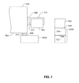
- FIG. 7 shows a side, cross-sectional view as seen from line 7 - 7 of FIG. 3 . The view of FIG. 7 is, therefore, upside down relative to the view of FIG. 6 .
- the structure 602 includes a portion 602 a that is configured to make contact with the lead pad 512 formed on the back side surface 504 of the slider 502 , and also includes a main body portion 602 b that connects with the main body of the test fixture 302 .
- the portion 602 b can include first and second semiconductor layers such as silicon (Si) 702 , 704 that can be separated from one another by an electrically insulating layer 706 .
- This structure can be referred to as a silicon on insulator structure.
- the portion 704 can be connected with the portion 302 by an adhesion layer 604 .
- the second layer 704 provides a spacer that allows the portion 602 a to contact that backside 504 of the slider 502 as desired.
- the structure 302 has an electrically conductive lead layer 312 that provides an electrically conductive contact point 310 that can engage and electrically connect with the contact pad 520 formed at the trailing edge of the slider 502 .
- the portion 602 a has an electrically conductive lead pad 606 that can engage with and make electrical connection with the lead pad 512 formed on the back side surface 504 of the slider 502 .
- a similar structure could be used to make contact with the lead pad 516 ( FIG. 5 ).
- test fixture 302 The structure of the test fixture 302 will be better understood with reference to FIGS. 8-30 which show the test fixture 302 in various intermediate stages of manufacture in order to illustrate a method for manufacturing a text fixture such as the test fixture 302 described above.
- a first layer of semiconductor such as Si 802 is deposited.
- An electrically insulating layer such as alumina (Al 2 O 3 ) 804 is deposited over the first semiconductor layer 802 , and a second semiconductor layer 302 is deposited over the electrically insulating layer 804 .
- a photoresist mask 902 is formed over the layers 802 , 804 , 302 .
- the photoresist mask is formed by depositing a photoresist material and then photolithographically patterning the photoresist material to form a pattern that defines a test fixture blank, with openings in the mask 902 that define the location where material will be removed.
- An example of a pattern that can be defined by the photoresist is shown in FIG. 10 where the lighter portions show the locations of the mask 902 and the darker portions show the locations of the under-lying layer 302 exposed through the openings in the mask 902 .
- a reactive ion etching is performed to remove portions of the layer 302 that are exposed through the openings in the mask 902 .
- the reactive ion etching can be terminated when the insulating layer 804 is reached. After the etching has been terminated, the mask 902 can be removed.
- an electrically conductive seed layer 1202 is deposited followed by a relatively thick layer of photoresist 1204 .
- the photoresist 1204 is photolithographically patterned to reduce the thickness of the photoresist 1204 only in a location where an electrically conductive lead will be formed as shown in FIG. 13 .
- FIG. 15 shows a top down view of the structure formed thus far as seen from line 15 - 15 of FIG. 14 .
- FIG. 15 shows how the lead lines 1402 extend from a slider contact end 1502 to a suspension contact end 1504 .
- a wafer support structure 1602 is bonded to the top of the previously formed structure by a bonding layer 1604 .
- the wafer support structure 1602 can be a Si wafer.
- a back grinding can be performed to remove the bottom semiconductor layer 802 , leaving a structure as shown in FIG. 17 .
- the wafer support structure 1602 provides support for the underlying layers during this back grinding.
- a dry etching process can be performed to remove the remaining insulation layer 804 , leaving a structure as shown in FIG. 18 .
- an adhesion material 1902 is applied to the bottom of the structure as shown in FIG. 19 .
- the adhesion material 1902 is preferably an adhesion tape. This adhesion tape 1902 will later be used to connect a structure for providing electrical contact with the backside surface of a slider. A material removal process can then be used to remove the bonding material 1604 and wafer support 1602 , leaving a structure as shown in FIG. 20 .
- FIGS. 21-27 describe a process for forming a test fixture portion configured for making contact with a backside lead contact of the slider.
- a double silicon on insulator structure is formed. This includes first second and third layers of semiconductor (preferably Si) 2102 , 702 , 704 .
- the first and second layers 2102 , 702 are separated from one another by a first layer of electrically insulating material such as alumina 2104 and the second and third semiconductor layers 702 , 704 are separated from one another by a second semiconductor layer 706 .
- a mask 2106 is formed over the layers 2102 , 2104 , 702 , 706 , 704 .
- the mask 2106 can be constructed of a photolithographically patterned photoresist and is configured to define the shape of a second test fixture layer that is configured to make contact with an electrical contact pad located on a backside surface of a slider.
- a reactive ion etching process can be performed to remove portion of layers 702 , 706 , 704 that are not protected by the mask 2106 , leaving a structure as shown in FIG. 22 .
- the mask 2302 can be formed by depositing a layer of photoresist and photolithographically patterning the photoresist so as to leave a portion of the underlying structure uncovered.
- the mask 2302 is constructed so as to expose a portion of the underlying structure that will be used to make contact with an electrical contact pad on the backside surface of the slider, as will be seen.
- a reactive ion etching can be performed to remove the portion of the layer 704 that is not protected by the mask 2302 . This reactive ion etching can be terminated when the layer 702 has been reached, leaving a structure as shown in FIG. 24 . After the reactive ion etching has been performed, the mask 2302 can be removed.
- an electrically conductive seed layer 2502 is deposited.
- the electrically conductive seed layer 2502 can be a material such as Cu or Au and can be deposited by sputter deposition. Then, a layer of electrically conductive lead material 2504 is electroplated over the seed layer 2502 .
- a photoresist mask 2602 is formed.
- the photoresist mask can be formed by depositing a layer of photoresist and photolithographically patterning the photoresist to leave an opening in a location where a contact pad will be formed.
- an electrically conductive material such as Cu or Au 2702 is electroplated into the opening in the mask 2602 .
- This electroplated electrically conductive material 2702 will form the contact pad 606 for making contact with the laser diode contact pad 512 at the backside surface of the slider 502 as shown in FIG. 7 .
- the photoresist 2602 is removed. Then, as shown in FIG. 28 , the first fixture layer 2802 (previous formed with reference to FIGS. 8-20 ) is bonded to the second test fixture portion 2804 (formed with reference to FIGS. 21-27 ).
- the first and second test fixture layers 2802 , 2804 can be bonded together by an adhesive such as the adhesive tape 1902 described above with reference to FIG. 19 .
- support structures 1602 and bonding material 1604 are present to support the first layer 2802 and support layers 802 , 804 are present to support the layer 2804 during bonding.
- a backside lapping process can be performed to remove layers 802 , 804 from the bottom of the second test claim layer 2804 .
- the layers 1604 , 1602 provide support during this lapping, leaving a structure as shown in FIG. 30 .
- a bond removal is performed to remove layers 1604 and 1602 , leaving a structure as shown in FIG. 30 .
Landscapes
- Adjustment Of The Magnetic Head Position Track Following On Tapes (AREA)
- Supporting Of Heads In Record-Carrier Devices (AREA)
Abstract
Description
Claims (18)
Priority Applications (1)
| Application Number | Priority Date | Filing Date | Title |
|---|---|---|---|
| US15/334,197 US9858954B1 (en) | 2016-10-25 | 2016-10-25 | Magnetic recording head test fixture for heat assisted magnetic recording head |
Applications Claiming Priority (1)
| Application Number | Priority Date | Filing Date | Title |
|---|---|---|---|
| US15/334,197 US9858954B1 (en) | 2016-10-25 | 2016-10-25 | Magnetic recording head test fixture for heat assisted magnetic recording head |
Publications (1)
| Publication Number | Publication Date |
|---|---|
| US9858954B1 true US9858954B1 (en) | 2018-01-02 |
Family
ID=60788785
Family Applications (1)
| Application Number | Title | Priority Date | Filing Date |
|---|---|---|---|
| US15/334,197 Active US9858954B1 (en) | 2016-10-25 | 2016-10-25 | Magnetic recording head test fixture for heat assisted magnetic recording head |
Country Status (1)
| Country | Link |
|---|---|
| US (1) | US9858954B1 (en) |
Cited By (3)
| Publication number | Priority date | Publication date | Assignee | Title |
|---|---|---|---|---|
| US20180240480A1 (en) * | 2017-02-23 | 2018-08-23 | Seagate Technology Llc | Slider test socket |
| US10679679B1 (en) * | 2018-12-21 | 2020-06-09 | Seagate Technology Llc | Slider test socket with clamp, and related assemblies and methods of use |
| US11105847B1 (en) | 2018-06-18 | 2021-08-31 | Seagate Technology Llc | Data storage component test socket opener |
Citations (22)
| Publication number | Priority date | Publication date | Assignee | Title |
|---|---|---|---|---|
| US5786962A (en) * | 1996-01-24 | 1998-07-28 | Sony Corporation | Magnetic head assembly |
| US6459260B1 (en) * | 2001-06-12 | 2002-10-01 | Seagate Technology Llc | Head suspension assembly for testing a slider |
| US6486660B1 (en) * | 2000-07-13 | 2002-11-26 | Seagate Technology Llc | Thermal slider level transfer curve tester for testing recording heads |
| US6943971B2 (en) * | 2002-08-26 | 2005-09-13 | Fujitsu Limited | Slider tester |
| US7355393B2 (en) * | 2005-07-15 | 2008-04-08 | Hitachi High-Technologies Corporation | Magnetic head slider testing apparatus and magnetic head slider testing method |
| US20090086374A1 (en) * | 2007-10-01 | 2009-04-02 | Seagate Technology Llc | High density electrical interconnect assembly |
| US7719796B2 (en) * | 2005-06-30 | 2010-05-18 | Hitachi Global Storage Technologies Netherlands B.V. | Suspension for hard disk drive which enables easy dynamic electric testing |
| JP2011108301A (en) | 2009-11-15 | 2011-06-02 | Hitachi Global Storage Technologies Netherlands Bv | Head gimbal assembly and method of manufacturing head slider |
| US7969826B2 (en) | 2006-11-16 | 2011-06-28 | Hitachi, Ltd. | Thermally assisted magnetic recording head having movable mirror for optical switching |
| US8089730B1 (en) * | 2009-10-28 | 2012-01-03 | Western Digital (Fremont), Llc | Suspension assembly having a read head clamp |
| US20120033318A1 (en) * | 2010-07-12 | 2012-02-09 | Zine-Eddine Boutaghou | Planar slider test socket |
| US20120049877A1 (en) * | 2009-06-02 | 2012-03-01 | Hsio Technologies, Llc | Compliant printed circuit peripheral lead semiconductor test socket |
| US8134804B2 (en) | 2008-04-01 | 2012-03-13 | Hitachi Global Storage Technologies Netherlands B.V. | Micro electro mechanical system and head gimbal assembly |
| US20120147717A1 (en) * | 2010-12-09 | 2012-06-14 | Rohm Co., Ltd. | Method of burn-in testing for thermally assisted head |
| US8384405B2 (en) * | 2011-04-20 | 2013-02-26 | Tdk Corporation | Method for performing burn-in test |
| US20130087455A1 (en) * | 2011-10-05 | 2013-04-11 | Joinsoon Medical Technology Co., Ltd. | Biosensor test strip |
| US8427783B2 (en) | 2008-11-19 | 2013-04-23 | HGST Netherlands B.V. | Head-gimbal assembly, microactuator, and manufacturing method of the microactuator |
| US8514522B1 (en) * | 2011-01-25 | 2013-08-20 | Western Digital (Fremont), Llc | Systems for interconnecting magnetic heads of storage devices in a test assembly |
| US8618828B2 (en) * | 2009-12-01 | 2013-12-31 | Nitto Denko Corporation | Connection structure of electronic component and wired circuit board, wired circuit board assembly, and method for testing electronic component |
| CN204022464U (en) | 2014-06-30 | 2014-12-17 | 华天科技(昆山)电子有限公司 | Three-dimensional MEMS encapsulating structure |
| US9013963B2 (en) * | 2012-04-25 | 2015-04-21 | Seagate Technology Llc | Flex circuit with dual sided interconnect structure |
| US9231328B2 (en) * | 2009-06-02 | 2016-01-05 | Hsio Technologies, Llc | Resilient conductive electrical interconnect |
-
2016
- 2016-10-25 US US15/334,197 patent/US9858954B1/en active Active
Patent Citations (23)
| Publication number | Priority date | Publication date | Assignee | Title |
|---|---|---|---|---|
| US5786962A (en) * | 1996-01-24 | 1998-07-28 | Sony Corporation | Magnetic head assembly |
| US6486660B1 (en) * | 2000-07-13 | 2002-11-26 | Seagate Technology Llc | Thermal slider level transfer curve tester for testing recording heads |
| US6459260B1 (en) * | 2001-06-12 | 2002-10-01 | Seagate Technology Llc | Head suspension assembly for testing a slider |
| US6943971B2 (en) * | 2002-08-26 | 2005-09-13 | Fujitsu Limited | Slider tester |
| US7719796B2 (en) * | 2005-06-30 | 2010-05-18 | Hitachi Global Storage Technologies Netherlands B.V. | Suspension for hard disk drive which enables easy dynamic electric testing |
| US7355393B2 (en) * | 2005-07-15 | 2008-04-08 | Hitachi High-Technologies Corporation | Magnetic head slider testing apparatus and magnetic head slider testing method |
| US7969826B2 (en) | 2006-11-16 | 2011-06-28 | Hitachi, Ltd. | Thermally assisted magnetic recording head having movable mirror for optical switching |
| US20090086374A1 (en) * | 2007-10-01 | 2009-04-02 | Seagate Technology Llc | High density electrical interconnect assembly |
| US8134804B2 (en) | 2008-04-01 | 2012-03-13 | Hitachi Global Storage Technologies Netherlands B.V. | Micro electro mechanical system and head gimbal assembly |
| US8427783B2 (en) | 2008-11-19 | 2013-04-23 | HGST Netherlands B.V. | Head-gimbal assembly, microactuator, and manufacturing method of the microactuator |
| US20120049877A1 (en) * | 2009-06-02 | 2012-03-01 | Hsio Technologies, Llc | Compliant printed circuit peripheral lead semiconductor test socket |
| US9231328B2 (en) * | 2009-06-02 | 2016-01-05 | Hsio Technologies, Llc | Resilient conductive electrical interconnect |
| US8089730B1 (en) * | 2009-10-28 | 2012-01-03 | Western Digital (Fremont), Llc | Suspension assembly having a read head clamp |
| JP2011108301A (en) | 2009-11-15 | 2011-06-02 | Hitachi Global Storage Technologies Netherlands Bv | Head gimbal assembly and method of manufacturing head slider |
| US8618828B2 (en) * | 2009-12-01 | 2013-12-31 | Nitto Denko Corporation | Connection structure of electronic component and wired circuit board, wired circuit board assembly, and method for testing electronic component |
| US20120033318A1 (en) * | 2010-07-12 | 2012-02-09 | Zine-Eddine Boutaghou | Planar slider test socket |
| US8395864B2 (en) * | 2010-07-12 | 2013-03-12 | Xyratex Technology Limited | Planar slider test socket |
| US20120147717A1 (en) * | 2010-12-09 | 2012-06-14 | Rohm Co., Ltd. | Method of burn-in testing for thermally assisted head |
| US8514522B1 (en) * | 2011-01-25 | 2013-08-20 | Western Digital (Fremont), Llc | Systems for interconnecting magnetic heads of storage devices in a test assembly |
| US8384405B2 (en) * | 2011-04-20 | 2013-02-26 | Tdk Corporation | Method for performing burn-in test |
| US20130087455A1 (en) * | 2011-10-05 | 2013-04-11 | Joinsoon Medical Technology Co., Ltd. | Biosensor test strip |
| US9013963B2 (en) * | 2012-04-25 | 2015-04-21 | Seagate Technology Llc | Flex circuit with dual sided interconnect structure |
| CN204022464U (en) | 2014-06-30 | 2014-12-17 | 华天科技(昆山)电子有限公司 | Three-dimensional MEMS encapsulating structure |
Non-Patent Citations (1)
| Title |
|---|
| Jianqiang et al., "Single Crystal Silicon MEMS Microactuator for High Density Hard Disk Drive," Device and Process Technologies for MEMS and Microelectronics II, 2001, pp. 1-7. |
Cited By (7)
| Publication number | Priority date | Publication date | Assignee | Title |
|---|---|---|---|---|
| US20180240480A1 (en) * | 2017-02-23 | 2018-08-23 | Seagate Technology Llc | Slider test socket |
| US10839836B2 (en) | 2017-02-23 | 2020-11-17 | Seagate Technology Llc | Slider test socket |
| US11105847B1 (en) | 2018-06-18 | 2021-08-31 | Seagate Technology Llc | Data storage component test socket opener |
| US10679679B1 (en) * | 2018-12-21 | 2020-06-09 | Seagate Technology Llc | Slider test socket with clamp, and related assemblies and methods of use |
| US11195559B2 (en) | 2018-12-21 | 2021-12-07 | Seagate Technology Llc | Slider test socket with clamp, and related assemblies and methods of use |
| US11705162B2 (en) | 2018-12-21 | 2023-07-18 | Seagate Technology Llc | Slider test clamp, and related assemblies and methods of use |
| US12014754B2 (en) * | 2018-12-21 | 2024-06-18 | Seagate Technology Llc | Clamp for removably holding a slider, and related assemblies and methods of use |
Similar Documents
| Publication | Publication Date | Title |
|---|---|---|
| US8164858B1 (en) | Read head having conductive filler in insulated hole through substrate | |
| US7710677B2 (en) | Thermally assisted magnetic head | |
| US8065788B2 (en) | Method for manufacturing a slider for a perpendicular magnetic recording head | |
| US9042062B2 (en) | Magnetic sensor with recessed AFM shape enhanced pinning and soft magnetic bias | |
| US7542236B2 (en) | Head slider, head gimbal assembly, and hard disk dirve | |
| US20050185345A1 (en) | Electrical lapping guide embedded in a shield of a magnetic head | |
| US7405909B2 (en) | Current perpendicular to plane (CPP) magnetoresistive sensor with free layer biasing by exchange pinning at back edge | |
| US8076246B2 (en) | Method of manufacturing thermally assisted magnetic head | |
| US6754056B2 (en) | Read head having a tunnel junction sensor with a free layer biased by exchange coupling with insulating antiferromagnetic (AFM) layers | |
| US10482905B2 (en) | Magnetic core and coil design for double perpendicular magnetic recording (PMR) writers | |
| US20040257706A1 (en) | Head slider, head gimbal assembly, and hard disk drive | |
| JP2007049136A (en) | Reluctance sensor having anisotropic hard bias without accompanying buffer layer | |
| US9858954B1 (en) | Magnetic recording head test fixture for heat assisted magnetic recording head | |
| US8161627B2 (en) | Method of making a write head lapping guide about aligned to a non-magnetic layer surrounding a write pole | |
| US7848061B2 (en) | Current perpendicular to plane (CPP) magnetoresistive sensor with back flux guide | |
| US8995091B2 (en) | Magnetic head for thermally assisted magnetic recording | |
| US8031434B2 (en) | Hybrid, self aligned magnetic write head with a partially plated pole and method of producing same | |
| US20050269288A1 (en) | Dual angle milling for current perpendicular to plane (CPP) magnetoresistive sensor definition | |
| US7870659B2 (en) | Method for defining a perpendicular magnetic head | |
| US7020959B2 (en) | Method of making conductive stud for magnetic recording devices | |
| JP2003196814A (en) | Thin film magnetic head slider and its manufacturing method | |
| US8082657B2 (en) | Method for manufacturing an electrical lapping guide for magnetic write head core width optimization | |
| US20170372732A1 (en) | Magnetic recording head test fixture having wrap-around contact pads | |
| US8225487B2 (en) | Method for confining sense current of a read transducer to an air-bearing surface(ABS) side of a free layer | |
| US20090168247A1 (en) | Magnetic head with embedded solder connection and method for manufacture thereof |
Legal Events
| Date | Code | Title | Description |
|---|---|---|---|
| AS | Assignment |
Owner name: WESTERN DIGITAL TECHNOLOGIES, INC., CALIFORNIA Free format text: ASSIGNMENT OF ASSIGNORS INTEREST;ASSIGNORS:SAIKI, NORIYUKI;KUDO, KAZUE;NIIMI, TAKAHARU;AND OTHERS;SIGNING DATES FROM 20161002 TO 20161015;REEL/FRAME:042029/0591 |
|
| STCF | Information on status: patent grant |
Free format text: PATENTED CASE |
|
| AS | Assignment |
Owner name: JPMORGAN CHASE BANK, N.A., AS AGENT, ILLINOIS Free format text: SECURITY INTEREST;ASSIGNOR:WESTERN DIGITAL TECHNOLOGIES, INC.;REEL/FRAME:052915/0566 Effective date: 20200113 |
|
| MAFP | Maintenance fee payment |
Free format text: PAYMENT OF MAINTENANCE FEE, 4TH YEAR, LARGE ENTITY (ORIGINAL EVENT CODE: M1551); ENTITY STATUS OF PATENT OWNER: LARGE ENTITY Year of fee payment: 4 |
|
| AS | Assignment |
Owner name: WESTERN DIGITAL TECHNOLOGIES, INC., CALIFORNIA Free format text: RELEASE OF SECURITY INTEREST AT REEL 052915 FRAME 0566;ASSIGNOR:JPMORGAN CHASE BANK, N.A.;REEL/FRAME:059127/0001 Effective date: 20220203 |
|
| AS | Assignment |
Owner name: JPMORGAN CHASE BANK, N.A., ILLINOIS Free format text: PATENT COLLATERAL AGREEMENT - A&R LOAN AGREEMENT;ASSIGNOR:WESTERN DIGITAL TECHNOLOGIES, INC.;REEL/FRAME:064715/0001 Effective date: 20230818 Owner name: JPMORGAN CHASE BANK, N.A., ILLINOIS Free format text: PATENT COLLATERAL AGREEMENT - DDTL LOAN AGREEMENT;ASSIGNOR:WESTERN DIGITAL TECHNOLOGIES, INC.;REEL/FRAME:067045/0156 Effective date: 20230818 |