US9831277B2 - Array substrate having an electro-static discharge unit, electro-static discharge method thereof and display device - Google Patents

Array substrate having an electro-static discharge unit, electro-static discharge method thereof and display device Download PDF

Info

Publication number
US9831277B2
US9831277B2 US15/222,136 US201615222136A US9831277B2 US 9831277 B2 US9831277 B2 US 9831277B2 US 201615222136 A US201615222136 A US 201615222136A US 9831277 B2 US9831277 B2 US 9831277B2
Authority
US
United States
Prior art keywords
signal line
switching transistor
electro
static discharge
charge release
Prior art date
Legal status (The legal status is an assumption and is not a legal conclusion. Google has not performed a legal analysis and makes no representation as to the accuracy of the status listed.)
Active
Application number
US15/222,136
Other versions
US20170110478A1 (en
Inventor
Cuili GAI
Quanhu LI
Current Assignee (The listed assignees may be inaccurate. Google has not performed a legal analysis and makes no representation or warranty as to the accuracy of the list.)
BOE Technology Group Co Ltd
Original Assignee
BOE Technology Group Co Ltd
Priority date (The priority date is an assumption and is not a legal conclusion. Google has not performed a legal analysis and makes no representation as to the accuracy of the date listed.)
Filing date
Publication date
Application filed by BOE Technology Group Co Ltd filed Critical BOE Technology Group Co Ltd
Assigned to BOE TECHNOLOGY GROUP CO., LTD. reassignment BOE TECHNOLOGY GROUP CO., LTD. ASSIGNMENT OF ASSIGNORS INTEREST (SEE DOCUMENT FOR DETAILS). Assignors: GAI, CUILI
Assigned to BOE TECHNOLOGY GROUP CO., LTD. reassignment BOE TECHNOLOGY GROUP CO., LTD. ASSIGNMENT OF ASSIGNORS INTEREST (SEE DOCUMENT FOR DETAILS). Assignors: LI, Quanhu
Publication of US20170110478A1 publication Critical patent/US20170110478A1/en
Application granted granted Critical
Publication of US9831277B2 publication Critical patent/US9831277B2/en
Active legal-status Critical Current
Anticipated expiration legal-status Critical

Links

Images

Classifications

    • HELECTRICITY
    • H10SEMICONDUCTOR DEVICES; ELECTRIC SOLID-STATE DEVICES NOT OTHERWISE PROVIDED FOR
    • H10DINORGANIC ELECTRIC SEMICONDUCTOR DEVICES
    • H10D86/00Integrated devices formed in or on insulating or conducting substrates, e.g. formed in silicon-on-insulator [SOI] substrates or on stainless steel or glass substrates
    • H10D86/40Integrated devices formed in or on insulating or conducting substrates, e.g. formed in silicon-on-insulator [SOI] substrates or on stainless steel or glass substrates characterised by multiple TFTs
    • H10D86/60Integrated devices formed in or on insulating or conducting substrates, e.g. formed in silicon-on-insulator [SOI] substrates or on stainless steel or glass substrates characterised by multiple TFTs wherein the TFTs are in active matrices
    • H01L27/124
    • H01L27/0266
    • HELECTRICITY
    • H10SEMICONDUCTOR DEVICES; ELECTRIC SOLID-STATE DEVICES NOT OTHERWISE PROVIDED FOR
    • H10DINORGANIC ELECTRIC SEMICONDUCTOR DEVICES
    • H10D86/00Integrated devices formed in or on insulating or conducting substrates, e.g. formed in silicon-on-insulator [SOI] substrates or on stainless steel or glass substrates
    • H10D86/40Integrated devices formed in or on insulating or conducting substrates, e.g. formed in silicon-on-insulator [SOI] substrates or on stainless steel or glass substrates characterised by multiple TFTs
    • H10D86/441Interconnections, e.g. scanning lines
    • HELECTRICITY
    • H10SEMICONDUCTOR DEVICES; ELECTRIC SOLID-STATE DEVICES NOT OTHERWISE PROVIDED FOR
    • H10DINORGANIC ELECTRIC SEMICONDUCTOR DEVICES
    • H10D89/00Aspects of integrated devices not covered by groups H10D84/00 - H10D88/00
    • H10D89/60Integrated devices comprising arrangements for electrical or thermal protection, e.g. protection circuits against electrostatic discharge [ESD]
    • H10D89/601Integrated devices comprising arrangements for electrical or thermal protection, e.g. protection circuits against electrostatic discharge [ESD] for devices having insulated gate electrodes, e.g. for IGFETs or IGBTs
    • H10D89/811Integrated devices comprising arrangements for electrical or thermal protection, e.g. protection circuits against electrostatic discharge [ESD] for devices having insulated gate electrodes, e.g. for IGFETs or IGBTs using FETs as protective elements
    • HELECTRICITY
    • H10SEMICONDUCTOR DEVICES; ELECTRIC SOLID-STATE DEVICES NOT OTHERWISE PROVIDED FOR
    • H10DINORGANIC ELECTRIC SEMICONDUCTOR DEVICES
    • H10D89/00Aspects of integrated devices not covered by groups H10D84/00 - H10D88/00
    • H10D89/60Integrated devices comprising arrangements for electrical or thermal protection, e.g. protection circuits against electrostatic discharge [ESD]
    • H10D89/601Integrated devices comprising arrangements for electrical or thermal protection, e.g. protection circuits against electrostatic discharge [ESD] for devices having insulated gate electrodes, e.g. for IGFETs or IGBTs
    • H10D89/921Integrated devices comprising arrangements for electrical or thermal protection, e.g. protection circuits against electrostatic discharge [ESD] for devices having insulated gate electrodes, e.g. for IGFETs or IGBTs characterised by the configuration of the interconnections connecting the protective arrangements, e.g. ESD buses

Definitions

  • Embodiments of the present disclosure pertain to an array substrate, an electro-static discharge method thereof and a display device.
  • flat panel displays have advantages such as low power consumption, small size, small weight, ultra thin screen and the like, compared with other kinds of displays, and are recently widely applied to, for example, intelligent devices, instruments, and low power consumption electronic products, which are controlled by single chip microcomputers or other controlling devices.
  • display panels mainly comprise two types: liquid crystal display panels and organic electroluminescent display panels.
  • conventional array substrates have poor ability of resisting electro-static damages, and electro-static damages often occur, which results in a short circuit between lines on the panel.
  • an organic electroluminescent display panel in the process of fabricating the array substrate thereof, a lot of electro-static discharges may occur in the process of cathode deposition. The electro-static discharges may seriously damage the array substrate, and the product yield is decreased.
  • An embodiment of the present disclosure provides an array substrate, comprising: a plurality of data lines, a plurality of gate lines, a power signal line, a charge release signal line, a plurality of electro-static discharge units and at least one short circuit ring unit, wherein, the charge release signal line and the power signal line are disposed in parallel, two electro-static discharge units are disposed between the charge release signal line and the power signal line to form an electro-static discharge circuit, each gate line and/or each data line is connected with the charge release signal line by one electro-static discharge unit; a first control terminal and a first input terminal of the short circuit ring unit are connected with the charge release signal line, a first output terminal is connected with the power signal line, a second control terminal and a second input terminal are connected with the power signal line, and a second output terminal is connected with the charge release signal line.
  • two adjacent gate lines and/or two adjacent data lines correspond to one short circuit ring unit.
  • the short circuit ring unit comprises: a first switching transistor and a second switching transistor; a gate electrode and a source electrode of the first switching transistor are both connected with the charge release signal line, and a drain electrode of the first switching transistor is connected with the power signal line; a gate electrode and a source electrode of the second switching transistor are both connected with the power signal line, and a drain electrode of the first switching transistor is connected with the charge release signal line.
  • At least one of the electro-static discharge units comprises: a third switching transistor and a fourth switching transistor.
  • the electro-static discharge unit, the power signal line and the charge release signal line constitute an electro-static discharge circuit, the gate electrode and the source electrode of the third switching transistor are both connected with the power signal line, and the drain electrode of the third switching transistor is connected with the charge release signal line; the gate electrode and the source electrode of the fourth switching transistor are both connected with the charge release signal line, and the drain electrode of the fourth switching transistor is connected with the power signal line.
  • the electro-static discharge unit connects the gate line and the charge release signal line, the gate electrode and the source electrode of the third switching transistor are both connected with the gate line, and the drain electrode of the third switching transistor is connected with the charge release signal line; the gate electrode and the source electrode of the fourth switching transistor are both connected with the charge release signal line, and the drain electrode of the fourth switching transistor is connected with the gate line.
  • the electro-static discharge unit connects the data line and the charge release signal line, the gate electrode and the source electrode of the third switching transistor are both connected with the data line, and the drain electrode of the third switching transistor is connected with the charge release signal line; the gate electrode and the source electrode of the fourth switching transistor are both connected with the charge release signal line, and the drain electrode of the fourth switching transistor is connected with the data line.
  • At least one of the electro-static discharge units comprises: a fifth switching transistor, a first capacitor and a second capacitor.
  • the electro-static discharge unit, the power signal line and the charge release signal line constitute an electro-static discharge circuit
  • the gate electrode of the fifth switching transistor connects with one end of the first capacitor and one end of the second capacitor respectively
  • the source electrode of the fifth switching transistor connects with the other end of the first capacitor and the power signal line respectively
  • the drain electrode of the fifth switching transistor connects with the other end of the second capacitor and the charge release signal line respectively.
  • the electro-static discharge unit connects the gate line and the charge release signal line
  • the gate electrode of the fifth switching transistor connects with one end of the first capacitor and one end of the second capacitor respectively
  • the source electrode of the fifth switching transistor connects with the other end of the first capacitor and the gate line
  • the drain electrode of the fifth switching transistor connects with the other end of the second capacitor and the charge release signal line.
  • the electro-static discharge unit connects the data line and the charge release signal line
  • the gate electrode of the fifth switching transistor connects with one end of the first capacitor and one end of the second capacitor respectively
  • the source electrode of the fifth switching transistor connects with the other end of the first capacitor and the data line respectively
  • the drain electrode of the fifth switching transistor connects with the other end of the second capacitor and the charge release signal line respectively.
  • the array substrate further comprises an organic electroluminescent structure comprising a cathode; the power signal line and the cathode of the organic electroluminescent structure are connected.
  • An embodiment of the present disclosure provides an electro-static discharge method of the array substrate mentioned above according to an embodiment of the present disclosure, comprising: upon static charges being generated on the power signal line, releasing the static charges to the electro-static discharge circuit through the short circuit ring unit; upon static charges being generated on the gate line or the data line, releasing the static charges to the charge release signal line through the electro-static discharge unit connected with the gate line or the data line, and releasing the static charges to the power signal line through the short circuit ring unit adjacent to the gate line or the data line.
  • An embodiment of the present disclosure provides an organic electroluminescent display panel, comprising the array substrate mentioned above according to an embodiment of the present disclosure.
  • An embodiment of the present disclosure provides a display device, comprising the organic electroluminescent display panel mentioned above according to an embodiment of the present disclosure.
  • FIG. 1 a and FIG. 1 b are structure schematic views of an array substrate according to an embodiment of the present disclosure
  • FIG. 2 a is a structure schematic view of a short circuit ring unit of an array substrate according to an embodiment of the present disclosure
  • FIG. 2 b is a schematic view showing electro-static discharge over a power signal line of an array substrate according to an embodiment of the present disclosure
  • FIG. 2 c is a schematic view showing electro-static discharge over a gate line of an array substrate according to an embodiment of the present disclosure.
  • FIG. 3 a and FIG. 3 b are structure schematic views of electro-static discharge units according to an embodiment of the present disclosure.
  • an electro-static discharge circuit is provided on the array substrate to release the static charges.
  • the electro-static discharge path is long, which results in that the electro-static discharge is not timely, and other lines on the substrate are prone to be damaged, thus lot of uncontrollable display defects are generated, and the product yield is decreased. Therefore, how to improve the poor ability of resisting static damages and resolve the problem of the long path of the electro-static discharge of the array substrate is before those skilled in the art.
  • An embodiment of the present disclosure provides an array substrate, as shown in FIG. 1 a and FIG. 1 b ( FIG. 1 a shows that short circuit ring units are disposed between adjacent gate lines, and FIG. 1 b shows that short circuit ring units are disposed between adjacent data lines),
  • the array substrate comprises: a plurality of data lines Dn, a plurality of gate lines Gn, a power signal line Vss, a charge release signal line Dh, and a plurality of electro-static discharge units ESD.
  • the charge release signal line Dh and the power signal line Vss are disposed in parallel, and two electro-static discharge units ESD are disposed between the charge release signal line Dh and the power signal line Vss to form an electro-static discharge circuit.
  • Each gate line Gn and/or each data line Dn is connected to the charge release signal line Dh by one electro-static discharge unit ESD.
  • the array substrate further comprises: at least one short circuit ring unit DR.
  • the short circuit ring unit is connected between the charge release signal line Dh and the power signal line Vss.
  • a first control terminal and a first input terminal of the short circuit ring unit DR are connected with the charge release signal line Dh; a first output terminal is connected with the power signal line Vss; a second control terminal and a second input terminal are connected with the power signal line Vss; and a second output terminal is connected with the charge release signal line Dh.
  • the short circuit ring unit is added.
  • the deposited cathode is connected with the power signal line of the electro-static discharge circuit, when lot of static charges are generated on the deposited cathode during deposition, lot of static charges are generated on the power signal line as well.
  • the static charges on the power signal line can be released to the electro-static discharge circuit through the short circuit ring unit.
  • the static charges on the gate line or on the data line can be released to the charge release signal line through the electro-static discharge unit that is connected with the gate line or the data line; and then the static charges are released to the power signal line quickly through the short circuit ring unit that is adjacent to the gate line or the data line, thus the static charges can be timely released.
  • the present embodiment can avoid the problem that the electro-static discharge is not timely, thus the performence of the array substrate is improved.
  • one short circuit ring unit is provided for two adjacent gate lines and/or two adjacent data lines correspondingly.
  • one short circuit ring unit can be disposed between every two adjacent gate lines and/or every two adjacent data lines.
  • the static charges generated at the location can be released to the power signal line Vss quickly through the switching transistor Tq that is turned on. Releasing of the static charges through the nearest short circuit ring unit can avoid the problem that the electro-static discharge is not timely, thus the efficiency of electro-static discharge is improved.
  • an example of the electro-static discharge unit comprises: a third switching transistor T 3 and a fourth switching transistor T 4 .
  • the electro-static discharge unit, the power signal line and the charge release signal line constitute an electro-static discharge circuit in combination.
  • the gate electrode and the source electrode of the third switching transistor T 3 are both connected with the power signal line, and the drain electrode thereof is connected with the charge release signal line.
  • the gate electrode and the source electrode of the fourth switching transistor T 4 are both connected with the charge release signal line, and the drain electrode thereof is connected with the power signal line.
  • the electro-static discharge unit connects a gate line and the charge release signal line.
  • the structure comprising the third switching transistor and the fourth switching transistor can realize the function of the electro-static discharge unit.
  • the structure can form an electro-static discharge circuit along with the power signal line and the charge release signal line, and can also release the static charges on the adjacent line, such as a gate line or a data line, to the electro-static discharge circuit quickly.
  • the electro-static discharge units of the embodiment are not limited to be of the same structure.
  • the gate electrode of the fifth switching transistor T 5 are connected with one end of the first capacitor C 1 and one end of the second capacitor C 2 respectively; the source electrode thereof is connected with the other end of the first capacitor C 1 and the gate line; and the drain electrode thereof is connected with the other end of the second capacitor C 2 and the charge release signal line.
  • the electro-static discharge unit connects the data line and the charge release signal line.
  • the gate electrode of the fifth switching transistor T 5 connects with one end of the first capacitor C 1 and one end of the second capacitor C 2 respectively; the source electrode thereof is connected with the other end of the first capacitor C 1 and the data line respectively; and the drain electrode thereof is connected with the other end of the second capacitor C 2 and the charge release signal line respectively.
  • the switching transistor mentioned in the embodiments above can be a thin film transistor (TFT), or can be a metal oxide semiconductor (MOS), the type of which is not limited herein.
  • the source electrode and the drain electrode of the transistor can be exchanged, which is not distinguished in structure. Only two exemplary the circuit structures of the electro-static discharge unit according to embodiments of the present disclosure are described. In some embodiments of the present disclosure, the electro-static discharge unit can be realized in other circuit structures which can realize the function of the electro-static discharge unit, which is not limited herein.
  • the array substrate according to embodiments of the present disclosure further comprises: an organic electroluminescent structure.
  • the power signal line and the cathode of the organic electroluminescent structure are connected.
  • static charges are easily generated in the deposition process of the cathode of the organic electroluminescent structure.
  • the cathode and the power signal line are connected, thus the static charges on the cathode can be released to the electro-static discharge circuit quickly; the static charges On other lines can be released to the electro-static discharge circuit through the short circuit ring unit, and finally released to the cathode. Because the static charges are released quickly, the problem that the electro-static discharge is not timely can be avoided.
  • An organic electroluminescent display panel comprises the array substrate mentioned above according to embodiments of the present disclosure. Because the principle to solve the problem of electro-static discharge of the organic electroluminescent display panel is similar to that of the array substrate, the examples of the array substrate can be referred to implement the organic electroluminescent display panel, which is not repeated herein.

Landscapes

  • Control Of Indicators Other Than Cathode Ray Tubes (AREA)
  • Devices For Indicating Variable Information By Combining Individual Elements (AREA)
  • Electroluminescent Light Sources (AREA)

Abstract

An array substrate, an electro-static discharge method thereof and a display device are disclosed. The array substrate includes: a plurality of data lines, a plurality of gate lines, a power signal line, a charge release signal line, a plurality of electro-static discharge units and at least one short circuit ring unit. The charge release signal line and the power signal line are disposed in parallel, two electro-static discharge units are disposed between them to form an electro-static discharge circuit, each gate line and/or each data line is connected with the charge release signal line by one electro-static discharge unit; the short circuit ring unit is connected between the charge release signal line and the power signal line.

Description

TECHNICAL FIELD
Embodiments of the present disclosure pertain to an array substrate, an electro-static discharge method thereof and a display device.
BACKGROUND
It is known that flat panel displays have advantages such as low power consumption, small size, small weight, ultra thin screen and the like, compared with other kinds of displays, and are recently widely applied to, for example, intelligent devices, instruments, and low power consumption electronic products, which are controlled by single chip microcomputers or other controlling devices.
Generally, display panels mainly comprise two types: liquid crystal display panels and organic electroluminescent display panels. As a core component of a display panel, the performance of an array substrate is especially important. However, conventional array substrates have poor ability of resisting electro-static damages, and electro-static damages often occur, which results in a short circuit between lines on the panel. Especially for an organic electroluminescent display panel, in the process of fabricating the array substrate thereof, a lot of electro-static discharges may occur in the process of cathode deposition. The electro-static discharges may seriously damage the array substrate, and the product yield is decreased.
SUMMARY
An embodiment of the present disclosure provides an array substrate, comprising: a plurality of data lines, a plurality of gate lines, a power signal line, a charge release signal line, a plurality of electro-static discharge units and at least one short circuit ring unit, wherein, the charge release signal line and the power signal line are disposed in parallel, two electro-static discharge units are disposed between the charge release signal line and the power signal line to form an electro-static discharge circuit, each gate line and/or each data line is connected with the charge release signal line by one electro-static discharge unit; a first control terminal and a first input terminal of the short circuit ring unit are connected with the charge release signal line, a first output terminal is connected with the power signal line, a second control terminal and a second input terminal are connected with the power signal line, and a second output terminal is connected with the charge release signal line.
For example, two adjacent gate lines and/or two adjacent data lines correspond to one short circuit ring unit.
For example, the short circuit ring unit comprises: a first switching transistor and a second switching transistor; a gate electrode and a source electrode of the first switching transistor are both connected with the charge release signal line, and a drain electrode of the first switching transistor is connected with the power signal line; a gate electrode and a source electrode of the second switching transistor are both connected with the power signal line, and a drain electrode of the first switching transistor is connected with the charge release signal line.
For example, at least one of the electro-static discharge units comprises: a third switching transistor and a fourth switching transistor. The electro-static discharge unit, the power signal line and the charge release signal line constitute an electro-static discharge circuit, the gate electrode and the source electrode of the third switching transistor are both connected with the power signal line, and the drain electrode of the third switching transistor is connected with the charge release signal line; the gate electrode and the source electrode of the fourth switching transistor are both connected with the charge release signal line, and the drain electrode of the fourth switching transistor is connected with the power signal line. Or the electro-static discharge unit connects the gate line and the charge release signal line, the gate electrode and the source electrode of the third switching transistor are both connected with the gate line, and the drain electrode of the third switching transistor is connected with the charge release signal line; the gate electrode and the source electrode of the fourth switching transistor are both connected with the charge release signal line, and the drain electrode of the fourth switching transistor is connected with the gate line. Or the electro-static discharge unit connects the data line and the charge release signal line, the gate electrode and the source electrode of the third switching transistor are both connected with the data line, and the drain electrode of the third switching transistor is connected with the charge release signal line; the gate electrode and the source electrode of the fourth switching transistor are both connected with the charge release signal line, and the drain electrode of the fourth switching transistor is connected with the data line.
For example, at least one of the electro-static discharge units comprises: a fifth switching transistor, a first capacitor and a second capacitor. The electro-static discharge unit, the power signal line and the charge release signal line constitute an electro-static discharge circuit, the gate electrode of the fifth switching transistor connects with one end of the first capacitor and one end of the second capacitor respectively, the source electrode of the fifth switching transistor connects with the other end of the first capacitor and the power signal line respectively, and the drain electrode of the fifth switching transistor connects with the other end of the second capacitor and the charge release signal line respectively. Or the electro-static discharge unit connects the gate line and the charge release signal line, the gate electrode of the fifth switching transistor connects with one end of the first capacitor and one end of the second capacitor respectively, the source electrode of the fifth switching transistor connects with the other end of the first capacitor and the gate line, and the drain electrode of the fifth switching transistor connects with the other end of the second capacitor and the charge release signal line. Or the electro-static discharge unit connects the data line and the charge release signal line, the gate electrode of the fifth switching transistor connects with one end of the first capacitor and one end of the second capacitor respectively, the source electrode of the fifth switching transistor connects with the other end of the first capacitor and the data line respectively, the drain electrode of the fifth switching transistor connects with the other end of the second capacitor and the charge release signal line respectively.
For example, the array substrate further comprises an organic electroluminescent structure comprising a cathode; the power signal line and the cathode of the organic electroluminescent structure are connected.
An embodiment of the present disclosure provides an electro-static discharge method of the array substrate mentioned above according to an embodiment of the present disclosure, comprising: upon static charges being generated on the power signal line, releasing the static charges to the electro-static discharge circuit through the short circuit ring unit; upon static charges being generated on the gate line or the data line, releasing the static charges to the charge release signal line through the electro-static discharge unit connected with the gate line or the data line, and releasing the static charges to the power signal line through the short circuit ring unit adjacent to the gate line or the data line.
An embodiment of the present disclosure provides an organic electroluminescent display panel, comprising the array substrate mentioned above according to an embodiment of the present disclosure.
An embodiment of the present disclosure provides a display device, comprising the organic electroluminescent display panel mentioned above according to an embodiment of the present disclosure.
BRIEF DESCRIPTION OF THE DRAWINGS
In order to clearly illustrate the technical solution of the embodiments of the disclosure, the drawings of the embodiments will be briefly described in the following; it is obvious that the described drawings are only related to some embodiments of the disclosure and thus are not limitative of the disclosure.
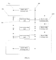
FIG. 1a and FIG. 1b are structure schematic views of an array substrate according to an embodiment of the present disclosure;
FIG. 2a is a structure schematic view of a short circuit ring unit of an array substrate according to an embodiment of the present disclosure;
FIG. 2b is a schematic view showing electro-static discharge over a power signal line of an array substrate according to an embodiment of the present disclosure;
FIG. 2c is a schematic view showing electro-static discharge over a gate line of an array substrate according to an embodiment of the present disclosure; and
FIG. 3a and FIG. 3b are structure schematic views of electro-static discharge units according to an embodiment of the present disclosure.
DETAILED DESCRIPTION
In order to make objects, technical details and advantages of the embodiments of the disclosure apparent, the technical solutions of the embodiments will be described in a clearly and fully understandable way in connection with the drawings related to the embodiments of the disclosure. Apparently, the described embodiments are just a part but not all of the embodiments of the disclosure. Based on the described embodiments herein, those skilled in the art can obtain other embodiment(s), without any inventive work, which should be within the scope of the disclosure.
In order to avoid the damage to an array substrate caused by the electro-static discharge, usually an electro-static discharge circuit is provided on the array substrate to release the static charges. However, the electro-static discharge path is long, which results in that the electro-static discharge is not timely, and other lines on the substrate are prone to be damaged, thus lot of uncontrollable display defects are generated, and the product yield is decreased. Therefore, how to improve the poor ability of resisting static damages and resolve the problem of the long path of the electro-static discharge of the array substrate is before those skilled in the art.
The array substrate, the electro-static discharge method thereof, and the display device according to embodiments of the present disclosure will be described in combination with the drawings in details as follows.
An embodiment of the present disclosure provides an array substrate, as shown in FIG. 1a and FIG. 1b (FIG. 1a shows that short circuit ring units are disposed between adjacent gate lines, and FIG. 1b shows that short circuit ring units are disposed between adjacent data lines), the array substrate comprises: a plurality of data lines Dn, a plurality of gate lines Gn, a power signal line Vss, a charge release signal line Dh, and a plurality of electro-static discharge units ESD. The charge release signal line Dh and the power signal line Vss are disposed in parallel, and two electro-static discharge units ESD are disposed between the charge release signal line Dh and the power signal line Vss to form an electro-static discharge circuit. Each gate line Gn and/or each data line Dn is connected to the charge release signal line Dh by one electro-static discharge unit ESD. The array substrate further comprises: at least one short circuit ring unit DR. The short circuit ring unit is connected between the charge release signal line Dh and the power signal line Vss.
In an example, a first control terminal and a first input terminal of the short circuit ring unit DR are connected with the charge release signal line Dh; a first output terminal is connected with the power signal line Vss; a second control terminal and a second input terminal are connected with the power signal line Vss; and a second output terminal is connected with the charge release signal line Dh.
In the array substrate mentioned above according to the embodiment of the present disclosure, the short circuit ring unit is added. In the fabricating process of the array substrate, because the deposited cathode is connected with the power signal line of the electro-static discharge circuit, when lot of static charges are generated on the deposited cathode during deposition, lot of static charges are generated on the power signal line as well. The static charges on the power signal line can be released to the electro-static discharge circuit through the short circuit ring unit. When static charges are generated on the gate line or on the data line, the static charges on the gate line or on the data line can be released to the charge release signal line through the electro-static discharge unit that is connected with the gate line or the data line; and then the static charges are released to the power signal line quickly through the short circuit ring unit that is adjacent to the gate line or the data line, thus the static charges can be timely released. Compared with the static charges release of the electro-static discharge circuit having a long discharge path, the present embodiment can avoid the problem that the electro-static discharge is not timely, thus the performence of the array substrate is improved.
As shown in FIG. 1a and FIG. 1b , in embodiments of the present disclosure, in the array substrate mentioned above, one short circuit ring unit is provided for two adjacent gate lines and/or two adjacent data lines correspondingly. For example, one short circuit ring unit can be disposed between every two adjacent gate lines and/or every two adjacent data lines. Thus, when static charges are generated on each gate line or each data line, the static charges can be released quickly through the corresponding short circuit ring unit. That is, static charges on each gate line or each data line can be released through the nearest short circuit ring unit, thus the efficiency of electro-static discharge is improved.
As shown in FIG. 2a , in embodiments of the present disclosure, an example of the short circuit ring unit of the array substrate mentioned above, for instance, comprises: a first switching transistor T1 and a second switching transistor T2. The gate electrode and the source electrode of the first switching transistor T1 are both connected with the charge release signal line Dh, and the drain electrode thereof is connected with the power signal line Vss; the gate electrode and the source electrode of the second switching transistor T2 are both connected with the power signal line Vss, and the drain electrode thereof is connected with the charge release signal line Dh. The short circuit ring unit mentioned above that comprises the first switching transistor and the second switching transistor can realize the function of quickly releasing of static charges on an adjacent line. For example, as shown in FIG. 2b , when static charges are generated on the power signal line at the location indicated by a dotted line box m, the switching transistor Tn that is nearest to the location indicated by the dotted line box m is turned on. Therefore, the static charges generated at the location can be released to the electro-static discharge circuit quickly through the switching transistor Tn that is turned on. For example, as shown in FIG. 2c , when static charges are generated on the gate line Gn at the location indicated by a dotted line box p, the static charges on the gate line Gn are released to the charge release signal line Dh through the electro-static discharge unit ESD corresponding to the gate line Gn; and the switching transistor Tq of the short circuit ring unit that is nearest to the gate line Gn is turned on. Therefore, the static charges generated at the location can be released to the power signal line Vss quickly through the switching transistor Tq that is turned on. Releasing of the static charges through the nearest short circuit ring unit can avoid the problem that the electro-static discharge is not timely, thus the efficiency of electro-static discharge is improved.
As shown in FIG. 3a , in the array substrate mentioned above according to embodiments of the present disclosure, an example of the electro-static discharge unit, for instance, comprises: a third switching transistor T3 and a fourth switching transistor T4. The electro-static discharge unit, the power signal line and the charge release signal line constitute an electro-static discharge circuit in combination. The gate electrode and the source electrode of the third switching transistor T3 are both connected with the power signal line, and the drain electrode thereof is connected with the charge release signal line. The gate electrode and the source electrode of the fourth switching transistor T4 are both connected with the charge release signal line, and the drain electrode thereof is connected with the power signal line. Alternatively, the electro-static discharge unit connects a gate line and the charge release signal line. The gate electrode and the source electrode of the third switching transistor T3 are both connected with the gate line, and the drain electrode thereof is connected with the charge release signal line. The gate electrode and the source electrode of the fourth switching transistor T4 are both connected with the charge release signal line, and the drain electrode thereof is connected with the gate line. Alternatively, the electro-static discharge unit connects a data line and the charge release signal line. The gate electrode and the source electrode of the third switching transistor T3 are both connected with the data line, and the drain electrode thereof is connected with the charge release signal line. The gate electrode and the source electrode of the fourth switching transistor T4 are both connected with the charge release signal line, and the drain electrode thereof is connected with the data line. In the array substrate mentioned above according to embodiments of the present disclosure, the structure comprising the third switching transistor and the fourth switching transistor can realize the function of the electro-static discharge unit. The structure can form an electro-static discharge circuit along with the power signal line and the charge release signal line, and can also release the static charges on the adjacent line, such as a gate line or a data line, to the electro-static discharge circuit quickly. The electro-static discharge units of the embodiment are not limited to be of the same structure.
As shown in FIG. 3b , in the array substrate mentioned above according to embodiments of the present disclosure, an example of the electro-static discharge unit, for instance, comprises: a fifth switching transistor T5, a first capacitor C1 and a second capacitor C2. The electro-static discharge unit, the power signal line and the charge release signal line constitute an electro-static discharge circuit. The gate electrode of the fifth switching transistor T5 is connected with one end of the first capacitor C1 and one end of the second capacitor C2 respectively; the source electrode thereof is connected with the other end of the first capacitor C1 and the power signal line respectively; and the drain electrode thereof is connected with the other end of the second capacitor C2 and the charge release signal line respectively. Alternatively, the electro-static discharge unit connects a gate line and the charge release signal line. The gate electrode of the fifth switching transistor T5 are connected with one end of the first capacitor C1 and one end of the second capacitor C2 respectively; the source electrode thereof is connected with the other end of the first capacitor C1 and the gate line; and the drain electrode thereof is connected with the other end of the second capacitor C2 and the charge release signal line. Alternatively, the electro-static discharge unit connects the data line and the charge release signal line. The gate electrode of the fifth switching transistor T5 connects with one end of the first capacitor C1 and one end of the second capacitor C2 respectively; the source electrode thereof is connected with the other end of the first capacitor C1 and the data line respectively; and the drain electrode thereof is connected with the other end of the second capacitor C2 and the charge release signal line respectively. In the array substrate mentioned above according to embodiments of the present disclosure, the structure comprising the fifth switching transistor the first capacitor and the second capacitor can realize the function of the electro-static discharge unit. The structure can form the electro-static discharge circuit along with the power signal line and the charge release signal line, and the static charges on an adjacent line, such as a gate line or a data line, can be released to the electro-static discharge circuit quickly. The electro-static discharge units of the embodiment are not limited to be of the same structure.
It should be noted that, the switching transistor mentioned in the embodiments above can be a thin film transistor (TFT), or can be a metal oxide semiconductor (MOS), the type of which is not limited herein. In some embodiments, the source electrode and the drain electrode of the transistor can be exchanged, which is not distinguished in structure. Only two exemplary the circuit structures of the electro-static discharge unit according to embodiments of the present disclosure are described. In some embodiments of the present disclosure, the electro-static discharge unit can be realized in other circuit structures which can realize the function of the electro-static discharge unit, which is not limited herein.
The array substrate according to embodiments of the present disclosure further comprises: an organic electroluminescent structure. The power signal line and the cathode of the organic electroluminescent structure are connected. In the array substrate according to embodiments of the present disclosure, static charges are easily generated in the deposition process of the cathode of the organic electroluminescent structure. The cathode and the power signal line are connected, thus the static charges on the cathode can be released to the electro-static discharge circuit quickly; the static charges On other lines can be released to the electro-static discharge circuit through the short circuit ring unit, and finally released to the cathode. Because the static charges are released quickly, the problem that the electro-static discharge is not timely can be avoided.
An electro-static discharge method of the array substrate mentioned above according to embodiments of the present disclosure comprises the following steps: upon static charges being generated on the power signal line, releasing the static charges to the electro-static discharge circuit through the short circuit ring unit; upon static charges being generated on a gate line or a data line, releasing the static charges to the charge release signal line through the electro-static discharge unit connected with the gate line or the data line, and releasing the static charges to the power signal line through the short circuit ring unit adjacent to the gate line or the data line.
In some embodiments of the present disclosure, when lot of static charges are generated on the power signal line, the static charges on the power signal line are released to the electro-static discharge circuit through the short circuit ring unit. When static charges are generated on a gate line or on a data line, the static charges on the gate line or on the data line are released to the charge release signal line through the electro-static discharge unit that is connected with the gate line or the data line; and then the static charges are released to the power signal line quickly through the short circuit ring unit that is adjacent to it, finally the static charges are timely released. Compared with the static charges release of the electro-static discharge circuit having a long discharge path, the present embodiment can avoid the problem that the electro-static discharge is not timely, thus the performence of the array substrate is improved.
An organic electroluminescent display panel according to an embodiment of the present disclosure comprises the array substrate mentioned above according to embodiments of the present disclosure. Because the principle to solve the problem of electro-static discharge of the organic electroluminescent display panel is similar to that of the array substrate, the examples of the array substrate can be referred to implement the organic electroluminescent display panel, which is not repeated herein.
A display device according to an embodiment of the present disclosure comprises the organic electroluminescent display panel mentioned above according to embodiments of the present disclosure. The display device can be any product or component having a display function such as mobile phone, tablet computer, television, display screen, laptop computer, digital photo frame, navigator or the like. Because the principle to solve the problem of electro-static discharge of the display device is similar to that of the organic electroluminescent display panel, the examples of the organic electroluminescent display panel can be referred to implement the display device, which is not repeated herein.
What are described above is related to the illustrative embodiments of the disclosure only and not limitative to the scope of the disclosure. Therefore, the scopes of the disclosure are defined by the accompanying claims.
The present application claims the priority of the Chinese Patent Application No. 201510673778.3 filed on Oct. 16, 2015, which is incorporated herein in its entirety by reference as part of the disclosure of the present application.

Claims (9)

What is claimed is:
1. An array substrate, comprising: a plurality of data lines, a plurality of gate lines, a power signal line, a charge release signal line, a plurality of electro-static discharge units and at least one short circuit ring unit, wherein,
the charge release signal line and the power signal line are disposed in parallel, two of the electro-static discharge units are disposed between the charge release signal line and the power signal line to form an electro-static discharge circuit, each of the gate lines and/or each of the data lines is connected with the charge release signal line by one of the electro-static discharge units;
a first control terminal and a first input terminal of the short circuit ring unit are connected with the charge release signal line, a first output terminal is connected with the power signal line, a second control terminal and a second input terminal are connected with the power signal line, and a second output terminal is connected with the charge release signal line.
2. The array substrate according to claim 1, wherein, two adjacent gate lines of the gate lines and/or two adjacent data lines of the data lines correspond to one short circuit ring unit.
3. The array substrate according to claim 2, wherein, the short circuit ring unit comprises: a first switching transistor and a second switching transistor,
a gate electrode and a source electrode of the first switching transistor are both connected with the charge release signal line, a drain electrode of the first switching transistor is connected with the power signal line; and
a gate electrode and a source electrode of the second switching transistor are both connected with the power signal line, a drain electrode of the second switching transistor is connected with the charge release signal line.
4. The array substrate according to claim 1, wherein, at least one of the electro-static discharge units comprises: a third switching transistor and a fourth switching transistor,
the electro-static discharge unit, the power signal line and the charge release signal line form an electro-static discharge circuit, a gate electrode and a source electrode of the third switching transistor are both connected with the power signal line, and a drain electrode of the third switching transistor is connected with the charge release signal line; a gate electrode and a source electrode of the fourth switching transistor are both connected with the charge release signal line, and a drain electrode of the fourth switching transistor is connected with the power signal line; or
the electro-static discharge unit connects the gate line and the charge release signal line, the gate electrode and the source electrode of the third switching transistor are both connected with the gate line, and the drain electrode of the third switching transistor is connected with the charge release signal line; the gate electrode and the source electrode of the fourth switching transistor are both connected with the charge release signal line, and the drain electrode of the fourth switching transistor is connected with the gate line; or
the electro-static discharge unit connects the data line and the charge release signal line, the gate electrode and the source electrode of the third switching transistor are both connected with the data line, and the drain electrode of the third switching transistor is connected with the charge release signal line; the gate electrode and the source electrode of the fourth switching transistor are both connected with the charge release signal line, and the drain electrode of the fourth switching transistor is connected with the data line.
5. The array substrate according to claim 1, wherein, at least one of the electro-static discharge units comprises: a fifth switching transistor, a first capacitor and a second capacitor,
the electro-static discharge unit, the power signal line and the charge release signal line form an electro-static discharge circuit, a gate electrode of the fifth switching transistor connects with one end of the first capacitor and one end of the second capacitor respectively, a source electrode of the fifth switching transistor connects with the other end of the first capacitor and the power signal line respectively, a drain electrode of the fifth switching transistor connects with the other end of the second capacitor and the charge release signal line respectively; or
the electro-static discharge unit connects the gate line and the charge release signal line, the gate electrode of the fifth switching transistor connects with one end of the first capacitor and one end of the second capacitor respectively, the source electrode of the fifth switching transistor connects with the other end of the first capacitor and the gate line, and the drain electrode of the fifth switching transistor connects with the other end of the second capacitor and the charge release signal line; or
the electro-static discharge unit connects the data line and the charge release signal line, the gate electrode of the fifth switching transistor connects with one end of the first capacitor and one end of the second capacitor respectively, the source electrode of the fifth switching transistor connects with the other end of the first capacitor and the data line respectively, and the drain electrode of the fifth switching transistor connects with the other end of the second capacitor and the charge release signal line respectively.
6. The array substrate according to claim 1, further comprising an organic electroluminescent structure comprising a cathode; wherein, the power signal line and the cathode of the organic electroluminescent structure are connected.
7. An electro-static discharge method of the array substrate according to claim 1 comprising:
upon static charges being generated on the power signal line, releasing the static charges to the electro-static discharge circuit through the short circuit ring unit; and
upon static charges being generated on the gate line or the data line, releasing the static charges to the charge release signal line through the electro-static discharge unit connected with the gate line or the data line, and releasing the static charges to the power signal line through the short circuit ring unit adjacent to the gate line or the data line.
8. An organic electroluminescent display panel, comprising the array substrate according to claim 1.
9. A display device, comprising the organic electroluminescent display panel according to claim 8.
US15/222,136 2015-10-16 2016-07-28 Array substrate having an electro-static discharge unit, electro-static discharge method thereof and display device Active US9831277B2 (en)

Applications Claiming Priority (3)

Application Number Priority Date Filing Date Title
CN201510673778.3A CN105304645B (en) 2015-10-16 2015-10-16 A kind of array base palte, its electrostatic release method and related device
CN201510673778.3 2015-10-16
CN201510673778 2015-10-16

Publications (2)

Publication Number Publication Date
US20170110478A1 US20170110478A1 (en) 2017-04-20
US9831277B2 true US9831277B2 (en) 2017-11-28

Family

ID=55201683

Family Applications (1)

Application Number Title Priority Date Filing Date
US15/222,136 Active US9831277B2 (en) 2015-10-16 2016-07-28 Array substrate having an electro-static discharge unit, electro-static discharge method thereof and display device

Country Status (2)

Country Link
US (1) US9831277B2 (en)
CN (1) CN105304645B (en)

Cited By (1)

* Cited by examiner, † Cited by third party
Publication number Priority date Publication date Assignee Title
US11570877B2 (en) 2020-02-13 2023-01-31 Boe Technology Group Co., Ltd. Display panel and display apparatus

Families Citing this family (9)

* Cited by examiner, † Cited by third party
Publication number Priority date Publication date Assignee Title
CN205450520U (en) * 2016-04-06 2016-08-10 京东方科技集团股份有限公司 Array substrate and display device
CN106200172B (en) * 2016-07-14 2020-06-02 京东方科技集团股份有限公司 Array substrate and display device
CN107785350A (en) * 2016-08-24 2018-03-09 中华映管股份有限公司 Electrostatic protection circuit and electrostatic protection method
CN107290908B (en) * 2017-06-23 2020-05-29 武汉华星光电技术有限公司 Electrostatic protection circuit and liquid crystal display panel
CN107589606A (en) 2017-09-05 2018-01-16 京东方科技集团股份有限公司 Array base palte and preparation method thereof, display device
CN107611952B (en) * 2017-09-14 2019-04-05 惠科股份有限公司 Electrostatic discharge protection circuit and display device using same
CN109698192B (en) * 2017-10-23 2021-01-22 京东方科技集团股份有限公司 Electrostatic protection circuit, array substrate and display device
CN208368505U (en) * 2018-08-03 2019-01-11 京东方科技集团股份有限公司 Electrostatic discharge protective circuit, array substrate and display device
CN110085584B (en) * 2019-04-29 2023-05-30 深圳市华星光电半导体显示技术有限公司 ESD protection thin film transistor and ESD protection structure

Citations (5)

* Cited by examiner, † Cited by third party
Publication number Priority date Publication date Assignee Title
US20040252117A1 (en) * 2003-06-13 2004-12-16 Semiconductor Energy Laboratory Co., Ltd. Display device
US20090289888A1 (en) * 2008-05-20 2009-11-26 Yoshiro Aoki Display device capable of reducing voltages in external integrated circuit
US20130215092A1 (en) * 2011-09-09 2013-08-22 Boe Technology Group Co., Ltd. Oled panel and method for driving the same
US20160163264A1 (en) * 2013-07-18 2016-06-09 Joled Inc. El display apparatus
US20170032738A1 (en) * 2015-07-29 2017-02-02 Samsung Display Co., Ltd. Organic light emitting display device and method of driving the same

Family Cites Families (5)

* Cited by examiner, † Cited by third party
Publication number Priority date Publication date Assignee Title
KR100386849B1 (en) * 2001-07-10 2003-06-09 엘지.필립스 엘시디 주식회사 Circuit for electro static dischrging of tft-lcd
US8692740B2 (en) * 2005-07-04 2014-04-08 Semiconductor Energy Laboratory Co., Ltd. Display device and driving method thereof
JP2007041096A (en) * 2005-08-01 2007-02-15 Sanyo Epson Imaging Devices Corp Electrooptical device, its manufacturing method, and electronic equipment
CN102629049B (en) * 2011-07-18 2015-05-20 京东方科技集团股份有限公司 Electrostatic protection structure, array substrate, liquid crystal panel and display device
CN104880881B (en) * 2015-06-25 2017-07-28 京东方科技集团股份有限公司 A kind of array base palte and its restorative procedure, display panel and display device

Patent Citations (5)

* Cited by examiner, † Cited by third party
Publication number Priority date Publication date Assignee Title
US20040252117A1 (en) * 2003-06-13 2004-12-16 Semiconductor Energy Laboratory Co., Ltd. Display device
US20090289888A1 (en) * 2008-05-20 2009-11-26 Yoshiro Aoki Display device capable of reducing voltages in external integrated circuit
US20130215092A1 (en) * 2011-09-09 2013-08-22 Boe Technology Group Co., Ltd. Oled panel and method for driving the same
US20160163264A1 (en) * 2013-07-18 2016-06-09 Joled Inc. El display apparatus
US20170032738A1 (en) * 2015-07-29 2017-02-02 Samsung Display Co., Ltd. Organic light emitting display device and method of driving the same

Cited By (1)

* Cited by examiner, † Cited by third party
Publication number Priority date Publication date Assignee Title
US11570877B2 (en) 2020-02-13 2023-01-31 Boe Technology Group Co., Ltd. Display panel and display apparatus

Also Published As

Publication number Publication date
US20170110478A1 (en) 2017-04-20
CN105304645A (en) 2016-02-03
CN105304645B (en) 2018-02-27

Similar Documents

Publication Publication Date Title
US9831277B2 (en) Array substrate having an electro-static discharge unit, electro-static discharge method thereof and display device
US9224760B2 (en) Array substrate and fabrication method thereof, and display device
US9759966B2 (en) Array substrate and method of manufacturing the same, and display device
US9638975B2 (en) Method for manufacturing COA liquid crystal panel comprising color resist blocks having first and second intersection zones and COA liquid crystal panel
US20230247871A1 (en) Display substrate and manufacturing method therefor, and display device
US9922996B2 (en) Array substrate, manufacturing method therefor and display device
US10204939B2 (en) Display substrate, manufacturing method thereof and display device
CN103456744B (en) Array base palte and preparation method thereof, display device
US20170083163A1 (en) Touch display circuit and driving method thereof, display apparatus
US20170200750A1 (en) Method for manufacturing array substrate
US20220326558A1 (en) Array substrate, display panel and display device
US10181422B2 (en) Array substrate, method for manufacturing the same, and display apparatus
US20220069056A1 (en) Array substrate, display device and electrostatic protection unit
US20180074642A1 (en) Touch display panel, driving method thereof and touch display device
CN104915054A (en) Array substrate and manufacturing method thereof and display device
WO2017036103A1 (en) Array substrate and display component
WO2020206811A1 (en) Tft array substrate, method for fabrication thereof, and display panel thereof
US20160293095A1 (en) Gate drive on array unit, gate drive on array circuit and display apparatus
CN105140235B (en) A kind of array substrate and display device
KR20180113627A (en) Charge-discharge circuit, display substrate, display device, and method of discharging charge therefrom
US9960276B2 (en) ESL TFT substrate structure and manufacturing method thereof
CN103985671A (en) Array substrate manufacturing method, array substrate and display device
US11335242B2 (en) Display substrate and display device
US20200365576A1 (en) Tft substrate, esd protection circuit and manufacturing method of tft substrate
CN108257974A (en) Array substrate, display device and the method for preparing array substrate

Legal Events

Date Code Title Description
AS Assignment

Owner name: BOE TECHNOLOGY GROUP CO., LTD., CHINA

Free format text: ASSIGNMENT OF ASSIGNORS INTEREST;ASSIGNOR:GAI, CUILI;REEL/FRAME:039282/0331

Effective date: 20160531

Owner name: BOE TECHNOLOGY GROUP CO., LTD., CHINA

Free format text: ASSIGNMENT OF ASSIGNORS INTEREST;ASSIGNOR:LI, QUANHU;REEL/FRAME:039282/0435

Effective date: 20160531

STCF Information on status: patent grant

Free format text: PATENTED CASE

MAFP Maintenance fee payment

Free format text: PAYMENT OF MAINTENANCE FEE, 4TH YEAR, LARGE ENTITY (ORIGINAL EVENT CODE: M1551); ENTITY STATUS OF PATENT OWNER: LARGE ENTITY

Year of fee payment: 4

MAFP Maintenance fee payment

Free format text: PAYMENT OF MAINTENANCE FEE, 8TH YEAR, LARGE ENTITY (ORIGINAL EVENT CODE: M1552); ENTITY STATUS OF PATENT OWNER: LARGE ENTITY

Year of fee payment: 8