US9825384B2 - Solderless edge connector - Google Patents
Solderless edge connector Download PDFInfo
- Publication number
- US9825384B2 US9825384B2 US15/395,438 US201615395438A US9825384B2 US 9825384 B2 US9825384 B2 US 9825384B2 US 201615395438 A US201615395438 A US 201615395438A US 9825384 B2 US9825384 B2 US 9825384B2
- Authority
- US
- United States
- Prior art keywords
- cuvette
- base component
- lead
- component
- assembly
- Prior art date
- Legal status (The legal status is an assumption and is not a legal conclusion. Google has not performed a legal analysis and makes no representation as to the accuracy of the status listed.)
- Active
Links
Images


Classifications
-
- H—ELECTRICITY
- H01—ELECTRIC ELEMENTS
- H01R—ELECTRICALLY-CONDUCTIVE CONNECTIONS; STRUCTURAL ASSOCIATIONS OF A PLURALITY OF MUTUALLY-INSULATED ELECTRICAL CONNECTING ELEMENTS; COUPLING DEVICES; CURRENT COLLECTORS
- H01R12/00—Structural associations of a plurality of mutually-insulated electrical connecting elements, specially adapted for printed circuits, e.g. printed circuit boards [PCB], flat or ribbon cables, or like generally planar structures, e.g. terminal strips, terminal blocks; Coupling devices specially adapted for printed circuits, flat or ribbon cables, or like generally planar structures; Terminals specially adapted for contact with, or insertion into, printed circuits, flat or ribbon cables, or like generally planar structures
- H01R12/70—Coupling devices
- H01R12/71—Coupling devices for rigid printing circuits or like structures
- H01R12/72—Coupling devices for rigid printing circuits or like structures coupling with the edge of the rigid printed circuits or like structures
- H01R12/721—Coupling devices for rigid printing circuits or like structures coupling with the edge of the rigid printed circuits or like structures cooperating directly with the edge of the rigid printed circuits
-
- G—PHYSICS
- G01—MEASURING; TESTING
- G01N—INVESTIGATING OR ANALYSING MATERIALS BY DETERMINING THEIR CHEMICAL OR PHYSICAL PROPERTIES
- G01N27/00—Investigating or analysing materials by the use of electric, electrochemical, or magnetic means
- G01N27/26—Investigating or analysing materials by the use of electric, electrochemical, or magnetic means by investigating electrochemical variables; by using electrolysis or electrophoresis
- G01N27/416—Systems
-
- H—ELECTRICITY
- H01—ELECTRIC ELEMENTS
- H01R—ELECTRICALLY-CONDUCTIVE CONNECTIONS; STRUCTURAL ASSOCIATIONS OF A PLURALITY OF MUTUALLY-INSULATED ELECTRICAL CONNECTING ELEMENTS; COUPLING DEVICES; CURRENT COLLECTORS
- H01R12/00—Structural associations of a plurality of mutually-insulated electrical connecting elements, specially adapted for printed circuits, e.g. printed circuit boards [PCB], flat or ribbon cables, or like generally planar structures, e.g. terminal strips, terminal blocks; Coupling devices specially adapted for printed circuits, flat or ribbon cables, or like generally planar structures; Terminals specially adapted for contact with, or insertion into, printed circuits, flat or ribbon cables, or like generally planar structures
- H01R12/70—Coupling devices
- H01R12/7005—Guiding, mounting, polarizing or locking means; Extractors
- H01R12/7011—Locking or fixing a connector to a PCB
- H01R12/7047—Locking or fixing a connector to a PCB with a fastener through a screw hole in the coupling device
-
- H—ELECTRICITY
- H01—ELECTRIC ELEMENTS
- H01R—ELECTRICALLY-CONDUCTIVE CONNECTIONS; STRUCTURAL ASSOCIATIONS OF A PLURALITY OF MUTUALLY-INSULATED ELECTRICAL CONNECTING ELEMENTS; COUPLING DEVICES; CURRENT COLLECTORS
- H01R13/00—Details of coupling devices of the kinds covered by groups H01R12/70 or H01R24/00 - H01R33/00
- H01R13/02—Contact members
- H01R13/193—Means for increasing contact pressure at the end of engagement of coupling part, e.g. zero insertion force or no friction
Definitions
- This document pertains generally, but not by way of limitation, to point-of-care analyzers for evaluating samples contained in a cuvette.
- Point-of-care analyzer instruments are used to evaluate biological samples collected from the patient at the time of collection of the sample or soon after collection.
- a cuvette is used to collect or receive collected biological sample and interface the sample with the analysis systems of the analyzer instrument.
- the cuvettes for receiving biological samples are advantageous as the cuvettes are typically disposable or reusable after washing.
- the cuvettes are also often configured to avoid directly contacting the collected sample with the circuitry for processing the samples, which would require the circuitry pins to be cleaned or replaced after each use to avoid contamination.
- a specialized connector is required to connect the cuvette to the analysis system and interface the sample with the pins of the analysis system. An improperly inserted cuvette can result in a poor connection between the cuvette and the pins, which can cause poor or inconsistent readings.
- a similar disadvantage is that the cuvette is typically small in size requiring the sensor interfaces to be tightly spaced on the cuvette.
- the tight spacing of the interfaces and the corresponding tight spacing of the pins can cause leakage current and other interference between the pins, which can further result in poor or inconsistent readings.
- a problem to be solved can include performing sensitive electrochemical analysis of a biological sample on a cuvette, where the sensor information from the cuvette is transmitted to a reader that is electrically connected to the cuvette.
- the tightly spaced pins and the corresponding circuits required to connect the cuvette to the reader can result in electrical leakage between adjacent circuits preventing the low ohm continuity and high pin-to-pin impedance.
- a problem to be solved can include that the sensitive electrochemical analysis often performed by the reader requires near-zero ohm continuity ( ⁇ 5 ⁇ ) between the pins while maintaining high pin-to-pin impedance (>5 G ⁇ ).
- the flux commonly used to solder leads or components to the circuit board can further increase the leakage between the adjacent circuits and leads. Other contaminants left on the connector assembly during construction or fluids on the cuvette or circuits can similarly create leakage between the leads.
- a solderless connector assembly for a reader assembly can include a base component and a clamp component that can be connected to the base component so as to retain at least one lead there between.
- the base component and the clamp component cooperate to retain the leads without soldering the leads, which can cause electrical leakage between adjacent leads.
- the reader can be portable to operate as a point-of-care analyzer where a cuvette can be connected to a circuit on board the reader via the at least one lead for evaluating a biological sample contained within the cuvette.
- the lead can have a cuvette end and a circuit end, where the lead is positioned between the base component and the clamp component such that the cuvette end and the circuit end protrude from between the base component and the clamp component.
- the circuit end of each lead can be positioned to contact a circuit pad of a circuit board, where the clamping of the connector assembly maintains the circuit end of the lead in contact with the circuit board. This arrangement removes the need to solder the lead to the circuit board removing a potential leakage point.
- the connector assembly can be removed from the circuit board without desoldering.
- a cuvette having a plurality of cuvette contacts can be positioned adjacent to the connector assembly such that the cuvette end engages the cuvette contacts to operably connect the cuvette to the circuit board.
- the cuvette end can be shaped such that positioning the cuvette such that the cuvette end of the lead engages the cuvette contacts and biases the lead maintaining contact between the lead and the cuvette contact.
- the base component can define at least one recessed track for receiving a lead, wherein securing the clamp component to the base component encloses each recessed track and isolates the recessed track from the adjacent recessed track.
- the clamp component can define at least one corresponding track mirroring one of the recessed tracks, wherein the recessed track and corresponding track cooperate to define a channel for receiving a lead.
- the base component and/or the clamp component can comprise a high impedance material to minimize electrical leakage between the adjacent tracks and the leads received therein.
- a reader can include a circuit board, at least one circuit pad, and a connector assembly, where the connector assembly can include a base component, a clamp component and at least one lead.
- the base component can define at least one recessed track for receiving each lead.
- the clamp component can be secured to the base component to clamp the at least one lead between the base component and the clamp component.
- the connector assembly can be operably engaged to the circuit board such that the lead between the base component and the clamp component engages a corresponding contact of the circuit.
- a point-of-care system can include a printed circuit board, a connector assembly, and a cuvette including at least one interface.
- the base component can define at least one recessed track for receiving each lead.
- the clamp component can be secured to the base component to clamp the at least one lead between the base component and the clamp component.
- the connector assembly can be operably engaged to the circuit board such that the lead between the base component and the clamp component engages a corresponding contact of the circuit.
- the cuvette can further include at least one cuvette contact, wherein the cuvette is moveable into an inserted position wherein the at least one cuvette contact is positioned to engage a cuvette end of the lead.
- FIG. 1 is a perspective view of a connector assembly connected to a sample fixture according to an example of the present disclosure with a cuvette inserted.
- FIG. 2 is a perspective exploded view of a solderless connector assembly according to an example of the present disclosure.
- FIG. 3 is a side view of a lead according to an example of the present disclosure.
- FIG. 4 is a perspective view of a solderless connector mounted to a PCB according to an example of the present disclosure with a cuvette inserted.
- FIG. 5 is a perspective view of the solderless connector and cuvette depicted in FIG. 4 in which a clamp component of the connector assembly is removed according to an example of the present disclosure.
- FIG. 6 is a perspective view of a solderless connector mounted to a PCB prior to cuvette insertion according to an example of the present disclosure.
- FIG. 7 is a partially transparent perspective view of a point-of-care analyzer according to an example of the present disclosure with a cuvette inserted.
- FIG. 8 is a perspective view of a point-of-care analyzer according to an example of the present disclosure with a cuvette inserted.
- FIG. 9 is a perspective exploded view of a connector assembly according to an example of the present disclosure.
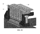
- FIG. 10 is a perspective view of a solderless connector as it is mounted to a PCB according to an example of the present disclosure.
- a reader 10 can include a frame 10 , a printed circuit board (“PCB”) 14 , at least one lead 16 and a connector assembly 18 .
- the reader 10 can be portable to operate as a point-of-care (“POC”) analyzer for evaluating cuvettes 20 containing biological samples.
- POC point-of-care
- the connector assembly 18 can be coupled to the frame 10 adjacent the PCB 14 to contact a PCB end 38 of the lead 16 with a contact of the PCB 14 and configured to retain the lead 16 against the PCB 14 .
- the cuvette end 40 of the lead 16 protrudes from the connector assembly 18 such that the cuvette 20 can be positioned against to the connector assembly 18 such that a cuvette contact of the cuvette 20 can engage the cuvette end 40 of the lead 16 .
- the analyzer frame 12 can define a slot for receiving the cuvette 20 and position the cuvette contacts of the cuvette 20 adjacent the leads 16 .
- the connector assembly 18 can include a base component 24 and a clamp component 26 .
- the base component 24 can define at least one recessed track 28 for receiving a lead 16 .
- the clamp component 26 can be secured to the base component 24 to enclose each recessed track 28 to retain the lead 16 within the track 28 .
- the clamp component 26 can include at least one corresponding track 30 cooperating with a recessed track 28 to define a channel for receiving the recessed track 28 .
- the base component 24 can be configured to receive at least one fastener 32 coupling the base component 24 to the analyzer frame 12 .
- the base component 24 can have notched portion for receiving the cuvette 20 and aligning the contacts of the cuvette 20 with the leads 16 .
- the clamp component 24 is configured to receive at least one fastening element 34 that can be engaged to a corresponding threaded hole 32 defined by the base component 24 .
- the fastening element 34 can be tightened to bias the clamp component 26 toward the base component 24 to retain the leads 16 between the clamp component 26 and the base component 24 .
- the base component 24 can define an angled surface to orient the leads 16 toward a cuvette 20 .
- the clamp component 26 can have a corresponding surface angled to complement the angled surface.
- the lead 16 extends from between the base component 24 and the clamp component 26 .
- the lead 16 can be flexible such that inserting the cuvette 20 flexes the lead 16 before the lead 16 biases into engagement with the interfaces of the cuvette 20 .
- At least one fastener 32 is inserted through the base component 24 to fix the base component 24 to the analyzer frame 12 .
- a fastening element 34 can be inserted through the clamp component 26 to tighten the clamp component 26 to the base component 24 and retain the leads 16 within the respective recessed track 28 such that the cuvette end 40 and the PCB end 38 of each lead 16 extends from between the base component 24 and the clamp component 26 .
- Each lead 16 can be positioned to reside within a recessed track 28 defined by the base component 24 such that the ends of the lead extend from recessed track of the base component 24 such that cuvette end 40 and the PCB end 38 protrude from the connector assembly 18 .
- each lead 16 can include a center portion 36 , a cuvette end 40 and a PCB end 38 .
- the cuvette end 40 is configured to engage the interfaces of the cuvette 20 and the PCB end 38 is configured to engage the interfaces 22 of the PCB 14 .
- the lead 16 can be interfaced with the PCB 14 without solder, which can damage the PCB 14 or provide leakage points impeding accurate results.
- the connector assembly 18 can be removed from the PCB 14 and replaced without requiring removal of the solder connecting the lead 16 to the PCB 14 .
- the cuvette end 40 can include a cuvette engagement feature 44 for engaging the interfaces of the cuvette 20 .
- the PCB end 38 can include a PCB engagement feature 42 for engaging the interfaces 22 of the PCB 14 .
- the center portion 36 can be received within the recessed track 28 such that the cuvette end 40 and the PCB end 38 extend from between the base component 24 and the clamp component 26 .
- the cuvette end 40 and the PCB end 38 can be flexibly connected to the center portion 36 such that the cuvette end 40 and the PCB end 38 can flex with respect to the center portion 36 .
- the flexibility of the cuvette end 40 can permit the flexing of the lead 16 as the cuvette 20 is inserted, which biases the cuvette end 40 against the contacts of the cuvette 20 .
- the cuvette end 40 can have variable thickness for engaging the contacts of the cuvette 20 .
- the cuvette end 40 can be thickened to increase the biasing force applied to the contacts of the cuvette 20 .
- the cuvette end 40 can be thinned to reduce the biasing force applied to the contacts of the cuvette 20 .
- the PCB end 38 can have variable thickness for engaging the interfaces 22 of the PCB 14 .
- the PCB end 38 can be thickened to increase the biasing force applied to the interfaces 22 of the PCB 14 .
- the PCB end 14 can be thinned to reduce the biasing force applied to the interfaces 22 of the PCB 14 .
- a cuvette 20 is inserted into the analyzer frame 12 such that the cuvette 20 is positioned adjacent the leads 16 .
- the exposed ends of the leads 16 flex as the cuvette 20 is inserted until the cuvette 20 is positioned in the inserted position. In the inserted position, the interfaces are aligned with the leads 16 such that the leads 16 bias from the flexed configuration to engage the interfaces of the cuvette 20 .
- the leads 16 flex as the cuvette 20 is drawn from the analyzer frame 12 and return to the original position when the cuvette 20 is withdrawn from the analyzer frame 12 .
- Example 1 is a circuit assembly comprising: an edge connector assembly including: a base component; a clamp component connected to the base component; at least one lead having a center portion, a circuit end, and a second circuit end; wherein the clamp component is configured to be tightened against the base component to secure the at least one lead there between; a printed circuit board having at least one circuit contact; wherein the edge connector assembly is fastened to the printed circuit assembly without requiring solder for either mechanical or electrical connection to the at least one circuit contact.
- an edge connector assembly including: a base component; a clamp component connected to the base component; at least one lead having a center portion, a circuit end, and a second circuit end; wherein the clamp component is configured to be tightened against the base component to secure the at least one lead there between; a printed circuit board having at least one circuit contact; wherein the edge connector assembly is fastened to the printed circuit assembly without requiring solder for either mechanical or electrical connection to the at least one circuit contact.
- Example 2 the subject matter of Example 1 optionally includes, wherein the base component defining at least one recessed track for receiving the at least one lead.
- Example 3 the subject matter of Example 2 optionally includes, wherein the recessed track is sized to receive the center portion of the at least one lead such that the circuit end and the cuvette end protrude from the connector assembly.
- Example 4 the subject matter of any one or more of Examples 1-3 optionally include, further comprising: an analyzer frame for receiving the printed circuit board.
- Example 5 the subject matter of Example 4 optionally includes, wherein the base component is configured to receive at least one fastener for coupling the base component to the analyzer frame adjacent the printed circuit board.
- Example 6 the subject matter of any one or more of Examples 4-5 optionally include, wherein the analyzer frame defines a slot for receiving the cuvette to position an interface of the cuvette in contact with the cuvette end of the lead.
- Example 8 the subject matter of Example 7 optionally includes, wherein the fastening element is adjustable such that the fastening element is selectively tightenable to adjust the tension applied to the leads positioned between the clamp component and the base component.
- Example 9 the subject matter of any one or more of Examples 1-8 optionally include, wherein the analyzer is a point-of-care analyzer.
- Example 10 is a point-of-care system, comprising: a printed circuit board having at least one circuit contact; a connector assembly include: a base component; a clamp component adjustably connected to the base component; at least one lead having a center portion, a circuit end, and a cuvette end, wherein the clamp component is configured to be tightened against the base component to secure the at least one lead such that the circuit end engage the circuit contact of the printed circuit board; a cuvette including at least one interface movable into an inserted position, wherein the interfaces of the cuvette are aligned with the PCB end of the corresponding lead when the cuvette is in the inserted position.
- Example 11 the subject matter of Example 10 optionally includes, wherein the base component defining at least one recessed track for receiving the at least one lead.
- Example 12 the subject matter of Example 11 optionally includes, wherein the recessed track is sized to receive the center portion of the at least one lead such that the circuit end and the cuvette end protrude from the connector assembly.
- Example 13 the subject matter of any one or more of Examples 10-12 optionally include, further comprising: an analyzer frame for receiving the printed circuit board.
- Example 14 the subject matter of Example 13 optionally includes, wherein the base component is configured to receive at least one fastener for coupling the base component to the analyzer frame adjacent the printed circuit board.
- Example 15 the subject matter of any one or more of Examples 13-14 optionally include, wherein the analyzer frame defines a slot for receiving the cuvette to position the circuit contact of the cuvette in contact with the cuvette end of the lead.
- Example 16 the subject matter of any one or more of Examples 10-15 optionally include, wherein the clamp component is configured to receive a fastening element for affixing the clamp component to the base component.
- the terms “a” or “an” are used, as is common in patent documents, to include one or more than one, independent of any other instances or usages of “at least one” or “one or more.”
- the term “or” is used to refer to a nonexclusive or, such that “A or B” includes “A but not B,” “B but not A,” and “A and B,” unless otherwise indicated.
- Method examples described herein can be machine or computer-implemented at least in part. Some examples can include a computer-readable medium or machine-readable medium encoded with instructions operable to configure an electronic device to perform methods as described in the above examples.
- An implementation of such methods can include code, such as microcode, assembly language code, a higher-level language code, or the like. Such code can include computer readable instructions for performing various methods. The code may form portions of computer program products. Further, in an example, the code can be tangibly stored on one or more volatile, non-transitory, or non-volatile tangible computer-readable media, such as during execution or at other times.
- Examples of these tangible computer-readable media can include, but are not limited to, hard disks, removable magnetic disks, removable optical disks (e.g., compact disks and digital video disks), magnetic cassettes, memory cards or sticks, random access memories (RAMs), read only memories (ROMs), and the like.
Abstract
Description
Claims (17)
Priority Applications (1)
| Application Number | Priority Date | Filing Date | Title |
|---|---|---|---|
| US15/395,438 US9825384B2 (en) | 2015-12-31 | 2016-12-30 | Solderless edge connector |
Applications Claiming Priority (2)
| Application Number | Priority Date | Filing Date | Title |
|---|---|---|---|
| US201562273836P | 2015-12-31 | 2015-12-31 | |
| US15/395,438 US9825384B2 (en) | 2015-12-31 | 2016-12-30 | Solderless edge connector |
Publications (2)
| Publication Number | Publication Date |
|---|---|
| US20170194730A1 US20170194730A1 (en) | 2017-07-06 |
| US9825384B2 true US9825384B2 (en) | 2017-11-21 |
Family
ID=59227047
Family Applications (1)
| Application Number | Title | Priority Date | Filing Date |
|---|---|---|---|
| US15/395,438 Active US9825384B2 (en) | 2015-12-31 | 2016-12-30 | Solderless edge connector |
Country Status (1)
| Country | Link |
|---|---|
| US (1) | US9825384B2 (en) |
Cited By (2)
| Publication number | Priority date | Publication date | Assignee | Title |
|---|---|---|---|---|
| US11121509B2 (en) * | 2019-04-12 | 2021-09-14 | Fci Connectors Dongguan Ltd. | Electrical connector |
| USD975024S1 (en) | 2019-04-12 | 2023-01-10 | Fci Connectors Dongguan Ltd. | Electrical connector |
Citations (5)
| Publication number | Priority date | Publication date | Assignee | Title |
|---|---|---|---|---|
| US4693529A (en) * | 1986-03-31 | 1987-09-15 | Amp Incorporated | Elastomeric mother-daughter board electrical connector |
| US5785534A (en) * | 1995-03-29 | 1998-07-28 | Siemens Aktiengesellschaft | Electrical connector |
| US6695646B1 (en) * | 2002-10-18 | 2004-02-24 | Hon Hai Precision Ind. Co., Ltd. | Electrical connector having floatable chicklets |
| US6918775B2 (en) * | 2003-09-23 | 2005-07-19 | Hon Hai Precision Ind. Co., Ltd. | Method for interconnecting multiple printed circuit boards |
| US7287986B2 (en) * | 2005-07-20 | 2007-10-30 | Molex Incorporated | Electrical connector |
-
2016
- 2016-12-30 US US15/395,438 patent/US9825384B2/en active Active
Patent Citations (5)
| Publication number | Priority date | Publication date | Assignee | Title |
|---|---|---|---|---|
| US4693529A (en) * | 1986-03-31 | 1987-09-15 | Amp Incorporated | Elastomeric mother-daughter board electrical connector |
| US5785534A (en) * | 1995-03-29 | 1998-07-28 | Siemens Aktiengesellschaft | Electrical connector |
| US6695646B1 (en) * | 2002-10-18 | 2004-02-24 | Hon Hai Precision Ind. Co., Ltd. | Electrical connector having floatable chicklets |
| US6918775B2 (en) * | 2003-09-23 | 2005-07-19 | Hon Hai Precision Ind. Co., Ltd. | Method for interconnecting multiple printed circuit boards |
| US7287986B2 (en) * | 2005-07-20 | 2007-10-30 | Molex Incorporated | Electrical connector |
Cited By (2)
| Publication number | Priority date | Publication date | Assignee | Title |
|---|---|---|---|---|
| US11121509B2 (en) * | 2019-04-12 | 2021-09-14 | Fci Connectors Dongguan Ltd. | Electrical connector |
| USD975024S1 (en) | 2019-04-12 | 2023-01-10 | Fci Connectors Dongguan Ltd. | Electrical connector |
Also Published As
| Publication number | Publication date |
|---|---|
| US20170194730A1 (en) | 2017-07-06 |
Similar Documents
| Publication | Publication Date | Title |
|---|---|---|
| BR0008927A (en) | Device for use in sample collection and testing and process for identifying an analyte of interest in a sample | |
| CA2730537C (en) | Strip connectors for measurement devices | |
| US9825384B2 (en) | Solderless edge connector | |
| WO2008051804A3 (en) | Method and apparatus for providing a stable voltage to an analytical system | |
| AU2003227690A1 (en) | Device and method for testing printed circuit boards, and testing probe for said device and method | |
| ATE535799T1 (en) | DOCKING STATION FOR A SENSOR CARTRIDGE | |
| HK1125999A1 (en) | Apparatus for the analysis of a sample on a test element | |
| US9791473B2 (en) | Test probe, test probe component and test platform | |
| WO2003029822A1 (en) | Specific binding analyzer and method of analyzing specific binding | |
| GB2439261A (en) | Analytical instrumentation apparatus and methods | |
| EP1503217A3 (en) | Electronic component test apparatus | |
| KR101059177B1 (en) | Relay connector | |
| ES2558873T3 (en) | Procedure and verification system of an electromechanical biosensor | |
| JP2009079905A (en) | Evaluation testing tool and evaluation testing electrode for electronic component | |
| GB2373575A (en) | Cam reference for inspection of multi-color and contour images | |
| TW200728728A (en) | A test card for integrated circuit (1) | |
| US11050208B2 (en) | Pre-screening, compliant pin guiding and quality monitoring press-fit apparatus | |
| US20200371167A1 (en) | Connector inspection apparatus and connector module | |
| WO2003019331A3 (en) | Method of conducting and documenting analyte screening tests | |
| ATE429634T1 (en) | MEASUREMENT ELEMENT FOR DETECTING TOTAL CHOLESTEROL IN A BLOOD SAMPLE | |
| KR100785309B1 (en) | Fpcb test jig | |
| US20190011494A1 (en) | Test probe and apparatus for testing printed circuit board | |
| CN219737691U (en) | Probe card base structure | |
| EP3621737B1 (en) | Retention clip and sample rack for a sample analysis system | |
| JPH0566243A (en) | Jig for lsi evaluation |
Legal Events
| Date | Code | Title | Description |
|---|---|---|---|
| AS | Assignment |
Owner name: LIFEHEALTH, LLC, MINNESOTA Free format text: ASSIGNMENT OF ASSIGNORS INTEREST;ASSIGNORS:KURKOWSKI, JAMES D.;BRASTAD, THOMAS PAUL;REEL/FRAME:042228/0987 Effective date: 20170412 |
|
| AS | Assignment |
Owner name: EASYDX, INC., MINNESOTA Free format text: ASSIGNMENT OF ASSIGNORS INTEREST;ASSIGNOR:DSI ASSIGNMENTS LLC;REEL/FRAME:043595/0554 Effective date: 20170907 Owner name: THE MICHAEL SINSHEIMER REVOCABLE TRUST U/A DATED 0 Free format text: RELEASE BY SECURED PARTY;ASSIGNOR:SIMCAH PARTNERS L.P.;REEL/FRAME:043747/0496 Effective date: 20170907 Owner name: LIFEHEALTH, LLC, MINNESOTA Free format text: RELEASE BY SECURED PARTY;ASSIGNOR:MICHAEL N. SINSHEIMER REVOCABLE TRUST U/A DATED 04/09/15;REEL/FRAME:043747/0483 Effective date: 20170907 Owner name: LIFEHEALTH, LLC, MINNESOTA Free format text: RELEASE BY SECURED PARTY;ASSIGNOR:SIMCAH PARTNERS L.P.;REEL/FRAME:043747/0496 Effective date: 20170907 Owner name: LIFEHEALTH, LLC, MINNESOTA Free format text: RELEASE BY SECURED PARTY;ASSIGNOR:PETERSON, MARK;REEL/FRAME:043865/0861 Effective date: 20170907 |
|
| AS | Assignment |
Owner name: EASYDX, INC., MINNESOTA Free format text: CORRECTIVE ASSIGNMENT TO CORRECT THE POSTAL CODE OF RECEIVING PARTY AND PCT NUMBER US1999014696 PREVIOUSLY RECORDED ON REEL 043595 FRAME 0554. ASSIGNOR(S) HEREBY CONFIRMS THE ASSIGNMENT;ASSIGNOR:DSI ASSIGNMENTS LLC;REEL/FRAME:043929/0162 Effective date: 20170907 |
|
| AS | Assignment |
Owner name: DSI ASSIGNMENTS LLC, SOLELY IN ITS CAPACITY AS ASS Free format text: ASSIGNMENT OF ASSIGNORS INTEREST;ASSIGNOR:LIFEHEALTH, LLC;REEL/FRAME:043759/0368 Effective date: 20170711 |
|
| STCF | Information on status: patent grant |
Free format text: PATENTED CASE |
|
| MAFP | Maintenance fee payment |
Free format text: PAYMENT OF MAINTENANCE FEE, 4TH YR, SMALL ENTITY (ORIGINAL EVENT CODE: M2551); ENTITY STATUS OF PATENT OWNER: SMALL ENTITY Year of fee payment: 4 |