US9820392B2 - Display apparatus and display apparatus manufacturing method - Google Patents
Display apparatus and display apparatus manufacturing method Download PDFInfo
- Publication number
- US9820392B2 US9820392B2 US15/126,076 US201415126076A US9820392B2 US 9820392 B2 US9820392 B2 US 9820392B2 US 201415126076 A US201415126076 A US 201415126076A US 9820392 B2 US9820392 B2 US 9820392B2
- Authority
- US
- United States
- Prior art keywords
- display panel
- base
- disposed
- component
- display apparatus
- Prior art date
- Legal status (The legal status is an assumption and is not a legal conclusion. Google has not performed a legal analysis and makes no representation as to the accuracy of the status listed.)
- Active
Links
Images


Classifications
-
- G—PHYSICS
- G02—OPTICS
- G02F—OPTICAL DEVICES OR ARRANGEMENTS FOR THE CONTROL OF LIGHT BY MODIFICATION OF THE OPTICAL PROPERTIES OF THE MEDIA OF THE ELEMENTS INVOLVED THEREIN; NON-LINEAR OPTICS; FREQUENCY-CHANGING OF LIGHT; OPTICAL LOGIC ELEMENTS; OPTICAL ANALOGUE/DIGITAL CONVERTERS
- G02F1/00—Devices or arrangements for the control of the intensity, colour, phase, polarisation or direction of light arriving from an independent light source, e.g. switching, gating or modulating; Non-linear optics
- G02F1/01—Devices or arrangements for the control of the intensity, colour, phase, polarisation or direction of light arriving from an independent light source, e.g. switching, gating or modulating; Non-linear optics for the control of the intensity, phase, polarisation or colour
- G02F1/13—Devices or arrangements for the control of the intensity, colour, phase, polarisation or direction of light arriving from an independent light source, e.g. switching, gating or modulating; Non-linear optics for the control of the intensity, phase, polarisation or colour based on liquid crystals, e.g. single liquid crystal display cells
- G02F1/133—Constructional arrangements; Operation of liquid crystal cells; Circuit arrangements
- G02F1/1333—Constructional arrangements; Manufacturing methods
- G02F1/133308—Support structures for LCD panels, e.g. frames or bezels
-
- H—ELECTRICITY
- H05—ELECTRIC TECHNIQUES NOT OTHERWISE PROVIDED FOR
- H05K—PRINTED CIRCUITS; CASINGS OR CONSTRUCTIONAL DETAILS OF ELECTRIC APPARATUS; MANUFACTURE OF ASSEMBLAGES OF ELECTRICAL COMPONENTS
- H05K5/00—Casings, cabinets or drawers for electric apparatus
- H05K5/0017—Casings, cabinets or drawers for electric apparatus with operator interface units
-
- H—ELECTRICITY
- H05—ELECTRIC TECHNIQUES NOT OTHERWISE PROVIDED FOR
- H05K—PRINTED CIRCUITS; CASINGS OR CONSTRUCTIONAL DETAILS OF ELECTRIC APPARATUS; MANUFACTURE OF ASSEMBLAGES OF ELECTRICAL COMPONENTS
- H05K5/00—Casings, cabinets or drawers for electric apparatus
- H05K5/02—Details
- H05K5/0217—Mechanical details of casings
-
- G—PHYSICS
- G02—OPTICS
- G02F—OPTICAL DEVICES OR ARRANGEMENTS FOR THE CONTROL OF LIGHT BY MODIFICATION OF THE OPTICAL PROPERTIES OF THE MEDIA OF THE ELEMENTS INVOLVED THEREIN; NON-LINEAR OPTICS; FREQUENCY-CHANGING OF LIGHT; OPTICAL LOGIC ELEMENTS; OPTICAL ANALOGUE/DIGITAL CONVERTERS
- G02F1/00—Devices or arrangements for the control of the intensity, colour, phase, polarisation or direction of light arriving from an independent light source, e.g. switching, gating or modulating; Non-linear optics
- G02F1/01—Devices or arrangements for the control of the intensity, colour, phase, polarisation or direction of light arriving from an independent light source, e.g. switching, gating or modulating; Non-linear optics for the control of the intensity, phase, polarisation or colour
- G02F1/13—Devices or arrangements for the control of the intensity, colour, phase, polarisation or direction of light arriving from an independent light source, e.g. switching, gating or modulating; Non-linear optics for the control of the intensity, phase, polarisation or colour based on liquid crystals, e.g. single liquid crystal display cells
- G02F1/133—Constructional arrangements; Operation of liquid crystal cells; Circuit arrangements
- G02F1/1333—Constructional arrangements; Manufacturing methods
- G02F1/133308—Support structures for LCD panels, e.g. frames or bezels
- G02F1/133314—Back frames
-
- G—PHYSICS
- G02—OPTICS
- G02F—OPTICAL DEVICES OR ARRANGEMENTS FOR THE CONTROL OF LIGHT BY MODIFICATION OF THE OPTICAL PROPERTIES OF THE MEDIA OF THE ELEMENTS INVOLVED THEREIN; NON-LINEAR OPTICS; FREQUENCY-CHANGING OF LIGHT; OPTICAL LOGIC ELEMENTS; OPTICAL ANALOGUE/DIGITAL CONVERTERS
- G02F1/00—Devices or arrangements for the control of the intensity, colour, phase, polarisation or direction of light arriving from an independent light source, e.g. switching, gating or modulating; Non-linear optics
- G02F1/01—Devices or arrangements for the control of the intensity, colour, phase, polarisation or direction of light arriving from an independent light source, e.g. switching, gating or modulating; Non-linear optics for the control of the intensity, phase, polarisation or colour
- G02F1/13—Devices or arrangements for the control of the intensity, colour, phase, polarisation or direction of light arriving from an independent light source, e.g. switching, gating or modulating; Non-linear optics for the control of the intensity, phase, polarisation or colour based on liquid crystals, e.g. single liquid crystal display cells
- G02F1/133—Constructional arrangements; Operation of liquid crystal cells; Circuit arrangements
- G02F1/1333—Constructional arrangements; Manufacturing methods
- G02F1/133308—Support structures for LCD panels, e.g. frames or bezels
- G02F1/13332—Front frames
Definitions
- the present disclosure relates to a display apparatus which includes a frame component disposed at a peripheral edge portion of a display panel, and a method for manufacturing a display apparatus for attaching the frame component to the display panel.
- Patent Literature 1 discloses a display apparatus which includes a frame component covering a peripheral edge portion of a display panel. With this display apparatus, the frame component functions as an escutcheon frame (protective frame) covering the entire peripheral edge of the display surface of the display panel on which images are displayed.
- the present disclosure provides a display apparatus which includes a frame component disposed at a peripheral edge portion of a display panel and pressed against or disposed in close vicinity to the display surface of the display panel, and a method for manufacturing such a display apparatus.
- the display apparatus includes: a display panel which displays an image; a base which is plate-shaped and disposed on a back side of the display panel opposite a display surface side on which the image is displayed; a frame component including a front surface portion disposed at a peripheral edge portion of the display panel on the display surface side, a fixing portion disposed on a back side of the base, and a connecting portion which is disposed exterior to a peripheral edge of the display panel and connects the front surface portion and the fixing portion; an attachment component including a base portion connected to the base, and a holding portion disposed further backward than the fixing portion of the frame component; and a fastening component which fastens the fixing portion and the holding portion of the attachment component.
- FIG. 1 is a cross section view illustrating a relationship between a display panel and a frame component of a conventional display apparatus.
- FIG. 2 is a perspective view illustrating an external appearance of a display apparatus according to Embodiment 1.
- FIG. 3 is an exploded perspective view illustrating an outline of the structure of a display apparatus according to Embodiment 1.
- FIG. 4 is a cross section view illustrating a relationship between a display panel and a frame component according to Embodiment 1.
- FIG. 5 is a perspective cross section view illustrating a relationship between a display panel and a frame component of a display apparatus.
- FIG. 6 is a perspective cross section view illustrating a relationship between a display panel and a frame component of a display apparatus with a back cover removed.
- FIG. 7 is a plan view illustrating, from the back side of a display apparatus, a relationship between attachment components and a frame component of the display apparatus with a back cover removed.
- FIG. 8 is a cross section view illustrating a relationship between a display panel and a frame component according to Variation 1 of Embodiment 1.
- FIG. 9 is a cross section view illustrating a relationship between a display panel and a frame component according to Variation 2 of Embodiment 1.
- FIG. 10 is a cross section view illustrating a relationship between a display panel and a frame component according to Variation 3 of Embodiment 1.
- the inventor has discovered the following problems related to a conventional display apparatus.
- FIG. 1 is a cross section view illustrating a relationship between a display panel and a frame component of a conventional display apparatus.
- a conventional display apparatus 500 for example, a display apparatus 500 having a liquid crystal display panel includes a display panel 501 which displays video and the like and a frame component 503 disposed to cover the respective edges of the display panel 501 and a base 502 that overlap with each other.
- the frame component 503 is a component with a C-shaped cross section, and has a groove 539 extending in the extending direction of the frame component 503 (Z axis direction in FIG. 1 ).
- the width of the groove 539 (length in Y axis direction in FIG. 1 ) is greater than the thickness of the overlapping display panel 501 and base 502 (length in Y axis direction in FIG. 1 ).
- a relatively thick gasket 509 filling a gap between the frame component 503 and the display panel 501 is attached to the inner surface of the groove 539 of the frame component 503 .
- the frame component 503 is disposed over the overlapping display panel 501 and base 502 in such a manner that the respective edges of the display panel 501 and the base 502 fit into the groove 539 of the frame component 503 , and then the frame component 503 and the base 502 are fastened using a fastening component 505 from the back side.
- the display apparatus 500 having such a structure, a gap is generated between the display panel 501 and the frame component 503 , and the frame component 503 protrudes to the front of the display panel 501 , resulting in a problem of degradation in the visibility and design of the display apparatus 500 .
- the gasket 509 deforms due to rubbing of the gasket 509 and the display panel 501 against each other when the frame component 503 is disposed, and that the gasket 509 adversely affects a resin sheet disposed on the front surface of the display panel 501 .
- FIG. 2 is a perspective view illustrating an external appearance of a display apparatus according to Embodiment 1.
- FIG. 3 is an exploded perspective view illustrating an outline of the structure of the display apparatus according to Embodiment 1.
- the display apparatus 100 includes a display panel 101 , a base 102 , a frame component 103 , attachment components 104 (not illustrated in FIG. 2 and FIG. 3 ), and fastening components 105 (not illustrated in FIG. 2 and FIG. 3 ).
- the display apparatus 100 is, for example, a television which outputs video and audio obtained from broadcast waves or the like received.
- the display apparatus 100 further includes circuit boards 129 and a back cover 106 which covers the back side of the display panel 101 .
- the display panel 101 is a device which displays an image, for example.
- the display panel 101 is an organic electroluminescent (EL) display panel which includes, as a light emitting element, an organic EL diode which is a light emitting diode having a luminescent layer made from an organic compound.
- the thickness of the display panel 101 is in a range from 1 mm to 3 mm approximately, for example.
- the type of the display panel 101 is not particularly limited, and may be, for example, a plasma display panel which is a self-luminous display panel like the organic EL display panel or a liquid crystal display panel which includes a back light unit.
- the thickness is also not particularly limited.
- the base 102 is component which is plate-shaped and disposed on the back side of the display panel 101 (the surface on the positive side of Y axis in figures), and holds the display panel 101 .
- the base 102 holds the circuit boards 129 on the back surface of the base 102 .
- the base 102 is, for example, made from a metal plate which is typically called a chassis, and may be provided with depressions and projections by a stamping process or the like to increase the structural strength, for example.
- a boss or the like may be attached to the base 102 for screwing.
- the base 102 is disposed to cover the entire (or almost the entire) back surface of the display panel 101 , and may have a function to dissipate heat generated by the display panel 101 .
- Each of the circuit boards 129 is formed by, for example, disposing an electric circuit including a plurality of electric components 80 on a board the base material of which is a resin plate.
- each circuit board 129 includes a circuit such as a signal processing circuit which processes a video signal received, a control circuit which controls operations of a scan driver circuit and a signal line driver circuit, or a power source circuit which receives electric power from outside and supplies the electric power to each circuit.
- FIG. 3 is an exemplary and schematic illustration of the circuit boards 129 , and not all the circuit boards 129 necessary for the display apparatus 100 are illustrated. Furthermore, the base 102 also holds a plurality of circuit boards having the above function but not illustrated in FIG. 3 . Specifically, such circuit boards are, for example, a scan driver circuit which supplies a scan drive signal to the display panel 101 and a signal line driver circuit which supplies a signal voltage to the display panel 101 . It should be noted that the scan driver circuit is also known as a gate driver or a scan driver, for example, and the signal line driver circuit is also known as a data driver or a source driver, for example.
- circuit boards not illustrated are disposed along the peripheral edge of the base 102 , and each circuit board and the display panel 101 are connected by a chip on film (COF) 200 , for example (see FIG. 4 ).
- COF chip on film
- FIG. 4 is a cross section view illustrating a relationship between the display panel and the frame component of the display apparatus according to the present embodiment.
- FIG. 5 is a perspective cross section view illustrating a relationship between the display panel and the frame component of the display apparatus.
- FIG. 6 is a perspective cross section view illustrating a relationship between the display panel and the frame component of the display apparatus with the back cover removed.
- the frame component 103 is a component which covers the respective peripheral edge portions of the display panel 101 and the base 102 that are disposed as overlapping layers.
- the frame component 103 is configured by assembling the following four components into a picture frame shape: two components covering the longer sides of the display panel 101 and the base 102 and two components covering the shorter sides of the display panel 101 and the base 102 .
- Each of the four components of the frame component 103 is a rod-shaped component which has a C-shaped cross section, includes a front surface portion 131 , fixing portions 132 , and a connecting portion 133 , and is formed by extrusion molding, for example.
- the front surface portion 131 is a portion of the frame component 103 which is disposed in close vicinity to or in contact with the peripheral edge portion of the display panel 101 on the display surface side.
- the front surface portion 131 may be in direct or indirect contact with the front surface of the display panel 101 .
- the front surface portion 131 is pressed against the display panel 101 by a certain pressure.
- This configuration makes it possible to reduce, to the extent possible, the gap generated between the display panel 101 and the front surface portion 131 of the frame component 103 , thereby enabling improvement in the visibility of the display panel 101 and in the design of the display apparatus 100 .
- Each of the fixing portions 132 is a portion of the frame component 103 which is disposed on the back side of the base 102 .
- Each fixing portion 132 is held by being fastened with a holding portion 141 (described later) of an attachment component 104 disposed further backward.
- the fixing portions 132 protrude toward the inside of the display apparatus 100 , and are disposed at predetermined intervals along the extending direction of the frame component 103 (that is, Z axis direction in FIG. 7 , but may also be X axis direction).
- each fixing portion 132 is formed by cutting out regions between the fixing portion 132 and adjacent fixing portions 132 .
- Wires, such as the COF 200 which connect the circuit boards 129 with electrodes disposed one level down from the front surface of the display panel 101 are disposed between adjacent fixing portions 132 .
- a force pressing the front surface portion 131 of the frame component 103 against the display panel 101 is generated based on the fastening force generated by fastening the fixing portions 132 and attachment components 104 .
- the COF 200 and the other wires etc. can be disposed without providing a cutout 138 between adjacent fixing portions 132 as illustrated in FIG. 7 .
- the frame component 103 is formed by extrusion molding, it is possible to omit the process of providing a cutout after the molding, thereby enabling an increase in the production efficiency of the display apparatus 100 .
- the fastening of the fixing portions 132 and the attachment components 104 does not necessarily have to generate the pressing force mentioned above.
- the front surface portion 131 can be disposed in close vicinity to or in contact with the front surface of the display panel 101 .
- the connecting portion 133 is a portion of the frame component 103 which is disposed exterior to the peripheral edge of the display panel 101 and connects the front surface portion 131 and the fixing portions 132 .
- the connecting portion 133 has a strength that allows the distance between the front surface portion 131 and the fixing portions 132 to be maintained constant.
- the connecting portion 133 conveys, to the front surface portion 131 , the force generated by the fastening of the fixing portions 132 and the attachment components 104 , so that the front surface portion 131 is pressed against the front surface of the display panel 101 .
- Each of the attachment components 104 is a component including a base portion 142 which is connected to the base 102 , and a holding portion 141 disposed further backward than a fixing portion 132 of the frame component 103 .
- each attachment component 104 is a component separate from the base 102 , and is attached to the base 102 through the fastening of the base portion 142 to the base 102 .
- the holding portion 141 is disposed with such spacing from the base 102 that, in a state in which the base portion 142 of the attachment component 104 is attached to the base 102 , the fixing portion 132 of the frame component 103 can be inserted between the holding portion 141 and the base 102 .
- the spacing between the holding portion 141 and the base 102 is at least greater than the thickness of the fixing portion 132 .
- a plurality of attachment components 104 are disposed on the base 102 to correspond to the fixing portions 132 of the frame component 103 .
- Wires such as the COF 200 and the circuit boards 129 may be disposed between adjacent fastening components 105 .
- the attachment components 104 are described as components separate from the base 102 , but are not limited to this.
- the present disclosure also includes the case where the base 102 is plastic-deformed by press molding or the like, causing part of the base 102 to function as the attachment components 104 .
- each attachment component 104 connects, through engagement or fastening, with the back cover 106 which covers the back side of the base 102 , and has a function to hold the back cover 106 on the back side of the base 102 .
- Each of the fastening components 105 is a component which fastens a fixing portion 132 and the holding portion 141 of an attachment component 104 .
- each fastening component 105 is a screw which generates a fastening force by threaded engagement.
- Each fastening component 105 is inserted into a hole provided in the holding portion 141 of an attachment component 104 and is threadedly engaged with a female screw provided in a fixing portion 132 , so as to fasten the fixing portion 132 and the holding portion 141 .
- each fastening component 105 is not limited to a screw which generates a fastening force by threaded engagement, and may be any component so long as it generates a fastening force, such as a rivet which generates a fastening force by plastic deformation or a snap which generates a fastening force by elastic force. Furthermore, even when at least one of the fixing portion 132 and the holding portion 141 generates a fastening force by engaging with the other through plastic deformation, for example, the portion generating the fastening force functions as a fastening component 105 .
- a boss or the like having a nut or a female screw may be fixed to the base 102 or the fixing portion 132 , for example, to generate a strong fastening force.
- the display panel 101 and the base 102 which is plate-shaped and disposed on the back side of the display panel 101 are stuck together using a double-sided adhesive tape, for example.
- the attachment components 104 are attached to the base 102 by fastening, for example.
- the fixing portions 132 of the frame component 103 are inserted between the base 102 and the holding portions 141 of the attachment components 104 while inserting, between the front surface portion 131 and the fixing portions 132 of the frame component 103 , the respective peripheral edges of the display panel 101 and the base 102 that are stuck together.
- the above fastening makes it possible to press the front surface portion 131 of the frame component 103 against the peripheral edge portion of the display panel 101 . It should be noted that instead of pressing the front surface portion 131 against the display panel 101 , the front surface portion 131 may be disposed in close vicinity to or in contact with the display panel 101 .
- the back cover 106 is fixed to the attachment components 104 by fastening, for example, so as to manufacture the display apparatus 100 .
- the display apparatus 100 and the method for manufacturing the display apparatus 100 described above by making the spacing between the front surface portion 131 and the fixing portions 132 of the frame component 103 relatively large, it is possible to easily insert the respective peripheral edge portions of the display panel 101 and the base 102 between the front surface portion 131 and the fixing portions 132 of the frame component 103 , and reduce, to the extent possible, the gap between the front surface of the display panel 101 and the front surface portion 131 of the frame component 103 .
- the display apparatus 100 employs an organic EL display panel, it is possible to increase the strength of the force pressing the front surface portion 131 of the frame component 103 against the display panel 101 , allowing an increase in the adhesion between the display panel 101 and the front surface portion 131 .
- FIG. 8 is a cross section view illustrating a relationship between the display panel and the frame component according to Variation 1 of Embodiment 1.
- the holding portions 141 of the attachment components 104 included in the display apparatus 100 are part of the back cover 106 which covers the back side of the base 102 . Furthermore, in Variation 1, the entire attachment components 104 , including the respective base portions 142 , are part of the back cover 106 .
- FIG. 9 is a cross section view illustrating a relationship between the display panel and the frame component according to Variation 2 of Embodiment 1.
- a cushioning component 139 may be disposed between the front surface portion 131 of the frame component 103 and the display panel 101 .
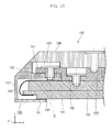
- FIG. 10 is a cross section view illustrating a relationship between the display panel and the frame component according to Variation 3 of Embodiment 1.
- the fixing portion 132 and the holding portion 141 of the attachment component 104 may be fastened by the fastening component 105 at a position further inward (closer to the center of the display panel 101 ) than an Inner edge 134 of the front surface portion 131 of the frame component 103 .
- the inner edge 134 of the front surface portion 131 of the frame component 103 fastened by the fastening component 105 is disposed further outward than the central axis C of the fastening component 105 in the plane parallel to the display surface of the display panel 101 (XZ plane in FIG. 10 ).
- being disposed “further outward than the fastening component 105 ” means not only being disposed further outward than the central axis C of the fastening component 105 . It is only necessary that the inner edge 134 be disposed further outward than an edge portion of the fastening component 105 on the inward side.
- the area of contact between the display panel 101 and the front surface portion 131 can be reduced while generating, with the fastening force generated by the fastening of the fixing portions 132 and the attachment components 104 , a force causing the front surface portion 131 of the frame component 103 to press the display panel 101 , thereby making it possible to achieve both the effect of reducing, to the extent possible, the gap between the display panel 101 and the front surface portion 131 and the effect of improving the design of the display apparatus 100 .
- Embodiment 1 and variations thereof are presented as examples of the technique disclosed in the present application.
- the technique according to the present disclosure is not limited to Embodiment 1 and variations thereof, and can also be applied to embodiments obtained through modification, replacement, addition, or omission to Embodiment 1 and variations thereof as necessary.
- the display apparatus 100 is assumed to be a television which includes an organic EL display panel.
- the display apparatus 100 may be an apparatus other than a television.
- the display apparatus 100 may be implemented as a monitor apparatus which displays video input from outside, digital signage used as advertising media, and a mobile terminal, a tablet terminal, and a table-type display apparatus which receive a user operation through a touch panel.
- the frame component 103 may be configured not only by assembling the rod-shaped components but also by assembling components among which at least the front surface portion 131 is a rectangular-looped one-piece component.
- the front surface portion 131 and the fixing portions 132 are made from separate components, disposed at the respective peripheral edges of the display panel 101 and the base 102 , and connected by the connecting portion 133 , so that the frame component 103 can be attached. This allows the front surface portion 131 to be formed into a frame shape seamlessly on the display surface side of the display apparatus 100 , thereby enabling improvement in the design of the display apparatus 100 .
- the present disclosure is applicable to a display apparatus which displays images, characters, and video, and for which a smaller frame is demanded.
- the present disclosure is applicable to electronic devices such as a television, a monitor display, digital signage, a mobile terminal, a tablet terminal, and a table-type display apparatus.
Landscapes
- Physics & Mathematics (AREA)
- Nonlinear Science (AREA)
- Mathematical Physics (AREA)
- Chemical & Material Sciences (AREA)
- Crystallography & Structural Chemistry (AREA)
- General Physics & Mathematics (AREA)
- Optics & Photonics (AREA)
- Engineering & Computer Science (AREA)
- Microelectronics & Electronic Packaging (AREA)
- Devices For Indicating Variable Information By Combining Individual Elements (AREA)
- Liquid Crystal (AREA)
Abstract
Description
Claims (6)
Applications Claiming Priority (3)
| Application Number | Priority Date | Filing Date | Title |
|---|---|---|---|
| JP2014057189 | 2014-03-19 | ||
| JP2014-057189 | 2014-03-19 | ||
| PCT/JP2014/006439 WO2015140865A1 (en) | 2014-03-19 | 2014-12-24 | Display apparatus and display apparatus manufacturing method |
Publications (2)
| Publication Number | Publication Date |
|---|---|
| US20170118848A1 US20170118848A1 (en) | 2017-04-27 |
| US9820392B2 true US9820392B2 (en) | 2017-11-14 |
Family
ID=54143891
Family Applications (1)
| Application Number | Title | Priority Date | Filing Date |
|---|---|---|---|
| US15/126,076 Active US9820392B2 (en) | 2014-03-19 | 2014-12-24 | Display apparatus and display apparatus manufacturing method |
Country Status (3)
| Country | Link |
|---|---|
| US (1) | US9820392B2 (en) |
| JP (1) | JP6311172B2 (en) |
| WO (1) | WO2015140865A1 (en) |
Families Citing this family (2)
| Publication number | Priority date | Publication date | Assignee | Title |
|---|---|---|---|---|
| CN107367859A (en) * | 2017-08-22 | 2017-11-21 | 惠科股份有限公司 | a display device |
| JP6873486B2 (en) * | 2018-08-06 | 2021-05-19 | 株式会社Joled | Display display device |
Citations (17)
| Publication number | Priority date | Publication date | Assignee | Title |
|---|---|---|---|---|
| US20030090458A1 (en) * | 2001-11-14 | 2003-05-15 | Canon Kabushiki Kaisha | Image display unit |
| US20050078465A1 (en) * | 2003-10-09 | 2005-04-14 | Sok-San Kim | Chassis base unit for plasma display device and plasma display device including the chassis base unit |
| JP2007094224A (en) | 2005-09-30 | 2007-04-12 | Hitachi Ltd | Display device |
| JP2008009164A (en) | 2006-06-29 | 2008-01-17 | Matsushita Electric Ind Co Ltd | Image display device |
| JP2008033093A (en) | 2006-07-31 | 2008-02-14 | Fujitsu Hitachi Plasma Display Ltd | Plasma display apparatus |
| US20080259542A1 (en) * | 2007-04-20 | 2008-10-23 | Coretronic Corporation | Plasma display |
| JP2009109886A (en) | 2007-10-31 | 2009-05-21 | Panasonic Corp | Display device |
| US20090261694A1 (en) * | 2008-04-17 | 2009-10-22 | Funai Electric Co., Ltd. | Flat panel display |
| JP2010181432A (en) | 2009-02-03 | 2010-08-19 | Canon Inc | Image display device |
| US20130003283A1 (en) * | 2011-06-28 | 2013-01-03 | Sony Corporation | Display device |
| JP2013174707A (en) | 2012-02-24 | 2013-09-05 | Sharp Corp | Display unit and television receiver |
| US20140085796A1 (en) * | 2012-09-26 | 2014-03-27 | Apple Inc. | Computer display or cover glass/cell attachment to frame |
| WO2015016209A1 (en) | 2013-07-30 | 2015-02-05 | シャープ株式会社 | Optical-member holding structure, display device, and television reception device |
| US8982546B2 (en) * | 2012-12-05 | 2015-03-17 | Quanta Computer Inc. | Electronic device |
| US20150208523A1 (en) * | 2014-01-22 | 2015-07-23 | Lg Electronics Inc. | Display device |
| US20150237291A1 (en) * | 2012-08-31 | 2015-08-20 | Sharp Kabushiki Kaisha | Display device, television receiver and electronic device |
| US9658649B2 (en) * | 2013-07-19 | 2017-05-23 | Lg Electronics Inc. | Display device and laptop computer |
-
2014
- 2014-12-24 JP JP2016508325A patent/JP6311172B2/en active Active
- 2014-12-24 US US15/126,076 patent/US9820392B2/en active Active
- 2014-12-24 WO PCT/JP2014/006439 patent/WO2015140865A1/en not_active Ceased
Patent Citations (17)
| Publication number | Priority date | Publication date | Assignee | Title |
|---|---|---|---|---|
| US20030090458A1 (en) * | 2001-11-14 | 2003-05-15 | Canon Kabushiki Kaisha | Image display unit |
| US20050078465A1 (en) * | 2003-10-09 | 2005-04-14 | Sok-San Kim | Chassis base unit for plasma display device and plasma display device including the chassis base unit |
| JP2007094224A (en) | 2005-09-30 | 2007-04-12 | Hitachi Ltd | Display device |
| JP2008009164A (en) | 2006-06-29 | 2008-01-17 | Matsushita Electric Ind Co Ltd | Image display device |
| JP2008033093A (en) | 2006-07-31 | 2008-02-14 | Fujitsu Hitachi Plasma Display Ltd | Plasma display apparatus |
| US20080259542A1 (en) * | 2007-04-20 | 2008-10-23 | Coretronic Corporation | Plasma display |
| JP2009109886A (en) | 2007-10-31 | 2009-05-21 | Panasonic Corp | Display device |
| US20090261694A1 (en) * | 2008-04-17 | 2009-10-22 | Funai Electric Co., Ltd. | Flat panel display |
| JP2010181432A (en) | 2009-02-03 | 2010-08-19 | Canon Inc | Image display device |
| US20130003283A1 (en) * | 2011-06-28 | 2013-01-03 | Sony Corporation | Display device |
| JP2013174707A (en) | 2012-02-24 | 2013-09-05 | Sharp Corp | Display unit and television receiver |
| US20150237291A1 (en) * | 2012-08-31 | 2015-08-20 | Sharp Kabushiki Kaisha | Display device, television receiver and electronic device |
| US20140085796A1 (en) * | 2012-09-26 | 2014-03-27 | Apple Inc. | Computer display or cover glass/cell attachment to frame |
| US8982546B2 (en) * | 2012-12-05 | 2015-03-17 | Quanta Computer Inc. | Electronic device |
| US9658649B2 (en) * | 2013-07-19 | 2017-05-23 | Lg Electronics Inc. | Display device and laptop computer |
| WO2015016209A1 (en) | 2013-07-30 | 2015-02-05 | シャープ株式会社 | Optical-member holding structure, display device, and television reception device |
| US20150208523A1 (en) * | 2014-01-22 | 2015-07-23 | Lg Electronics Inc. | Display device |
Non-Patent Citations (1)
| Title |
|---|
| International Search Report, along with English-language translation thereof, in PCT/JP2014/006439 dated Mar. 17, 2015. |
Also Published As
| Publication number | Publication date |
|---|---|
| US20170118848A1 (en) | 2017-04-27 |
| JP6311172B2 (en) | 2018-04-18 |
| JPWO2015140865A1 (en) | 2017-04-06 |
| WO2015140865A1 (en) | 2015-09-24 |
Similar Documents
| Publication | Publication Date | Title |
|---|---|---|
| US7683541B2 (en) | Display apparatus provided with movable substrate covers securing edges of a front cover and its corresponding reinforcing plate | |
| US10554797B2 (en) | Mobile terminal, shell module, display module, and method of assembling display module | |
| US9025104B2 (en) | Backboard structure, backlight module, liquid crystal display module | |
| US11650635B2 (en) | Image display device | |
| US10098244B2 (en) | Image display apparatus and image display apparatus manufacturing method | |
| CN107544171A (en) | Display device | |
| JP2012037672A (en) | Display device | |
| US20160309598A1 (en) | Display apparatus | |
| US20180107048A1 (en) | Display module and display device | |
| US9820392B2 (en) | Display apparatus and display apparatus manufacturing method | |
| JP2015219387A (en) | Display device | |
| US10687445B2 (en) | Organic EL display apparatus | |
| JP2014224939A (en) | Display apparatus | |
| US10274772B2 (en) | Display device | |
| US20150109742A1 (en) | Display device | |
| EP3264400B1 (en) | Back plate for use in a display device and display device comprising such a back plate | |
| KR102300952B1 (en) | Structure for fixing pem nut | |
| US9894784B2 (en) | Display apparatus | |
| KR102094888B1 (en) | Display device | |
| US20150156897A1 (en) | Display device | |
| TWI590120B (en) | Integrated backlight module touch display module and its manufacturing method | |
| JP6821499B2 (en) | Exterior structure | |
| WO2014192205A1 (en) | Substrate holder, electronic apparatus, and display device |
Legal Events
| Date | Code | Title | Description |
|---|---|---|---|
| AS | Assignment |
Owner name: JOLED INC., JAPAN Free format text: ASSIGNMENT OF ASSIGNORS INTEREST;ASSIGNOR:MATSUI, HITOSHI;REEL/FRAME:039740/0447 Effective date: 20160804 |
|
| STCF | Information on status: patent grant |
Free format text: PATENTED CASE |
|
| MAFP | Maintenance fee payment |
Free format text: PAYMENT OF MAINTENANCE FEE, 4TH YEAR, LARGE ENTITY (ORIGINAL EVENT CODE: M1551); ENTITY STATUS OF PATENT OWNER: LARGE ENTITY Year of fee payment: 4 |
|
| AS | Assignment |
Owner name: INCJ, LTD., JAPAN Free format text: SECURITY INTEREST;ASSIGNOR:JOLED, INC.;REEL/FRAME:063396/0671 Effective date: 20230112 |
|
| AS | Assignment |
Owner name: JOLED, INC., JAPAN Free format text: CORRECTION BY AFFIDAVIT FILED AGAINST REEL/FRAME 063396/0671;ASSIGNOR:JOLED, INC.;REEL/FRAME:064067/0723 Effective date: 20230425 |
|
| AS | Assignment |
Owner name: JDI DESIGN AND DEVELOPMENT G.K., JAPAN Free format text: ASSIGNMENT OF ASSIGNORS INTEREST;ASSIGNOR:JOLED, INC.;REEL/FRAME:066382/0619 Effective date: 20230714 |
|
| MAFP | Maintenance fee payment |
Free format text: PAYMENT OF MAINTENANCE FEE, 8TH YEAR, LARGE ENTITY (ORIGINAL EVENT CODE: M1552); ENTITY STATUS OF PATENT OWNER: LARGE ENTITY Year of fee payment: 8 |
|
| AS | Assignment |
Owner name: MAGNOLIA BLUE CORPORATION, JAPAN Free format text: ASSIGNMENT OF ASSIGNORS INTEREST;ASSIGNOR:JDI DESIGN AND DEVELOPMENT G.K.;REEL/FRAME:072039/0656 Effective date: 20250625 |