US9809672B2 - Aromatic resins for underlayers - Google Patents
Aromatic resins for underlayers Download PDFInfo
- Publication number
- US9809672B2 US9809672B2 US15/363,114 US201615363114A US9809672B2 US 9809672 B2 US9809672 B2 US 9809672B2 US 201615363114 A US201615363114 A US 201615363114A US 9809672 B2 US9809672 B2 US 9809672B2
- Authority
- US
- United States
- Prior art keywords
- aryl
- alkyl
- layer
- reaction product
- substituted
- Prior art date
- Legal status (The legal status is an assumption and is not a legal conclusion. Google has not performed a legal analysis and makes no representation as to the accuracy of the status listed.)
- Active
Links
- 125000003118 aryl group Chemical group 0.000 title claims description 89
- 229920005989 resin Polymers 0.000 title description 57
- 239000011347 resin Substances 0.000 title description 57
- 239000007795 chemical reaction product Substances 0.000 claims abstract description 52
- -1 aromatic alcohols Chemical class 0.000 claims abstract description 28
- 238000004519 manufacturing process Methods 0.000 claims abstract description 9
- 239000000758 substrate Substances 0.000 claims description 48
- 238000000034 method Methods 0.000 claims description 42
- 229920002120 photoresistant polymer Polymers 0.000 claims description 33
- 239000000203 mixture Substances 0.000 claims description 28
- 239000002253 acid Substances 0.000 claims description 26
- 239000000178 monomer Substances 0.000 claims description 25
- XUIMIQQOPSSXEZ-UHFFFAOYSA-N Silicon Chemical compound [Si] XUIMIQQOPSSXEZ-UHFFFAOYSA-N 0.000 claims description 24
- 229910052710 silicon Inorganic materials 0.000 claims description 24
- 239000010703 silicon Substances 0.000 claims description 24
- 239000002904 solvent Substances 0.000 claims description 23
- 125000000739 C2-C30 alkenyl group Chemical group 0.000 claims description 17
- 238000005530 etching Methods 0.000 claims description 15
- 150000007513 acids Chemical class 0.000 claims description 10
- 239000003431 cross linking reagent Substances 0.000 claims description 9
- 239000003795 chemical substances by application Substances 0.000 claims description 8
- 239000003960 organic solvent Substances 0.000 claims description 8
- 239000004094 surface-active agent Substances 0.000 claims description 7
- 230000005855 radiation Effects 0.000 claims description 6
- 125000003358 C2-C20 alkenyl group Chemical group 0.000 claims description 5
- 229910052500 inorganic mineral Inorganic materials 0.000 claims description 5
- 239000011707 mineral Chemical class 0.000 claims description 5
- 239000000654 additive Substances 0.000 claims description 4
- ZUOUZKKEUPVFJK-UHFFFAOYSA-N diphenyl Chemical group C1=CC=CC=C1C1=CC=CC=C1 ZUOUZKKEUPVFJK-UHFFFAOYSA-N 0.000 claims description 4
- 125000002887 hydroxy group Chemical group [H]O* 0.000 claims description 4
- 150000003460 sulfonic acids Chemical class 0.000 claims description 4
- 125000001624 naphthyl group Chemical group 0.000 claims description 3
- 238000000059 patterning Methods 0.000 claims description 3
- 125000000094 2-phenylethyl group Chemical group [H]C1=C([H])C([H])=C(C([H])=C1[H])C([H])([H])C([H])([H])* 0.000 claims description 2
- 125000001797 benzyl group Chemical group [H]C1=C([H])C([H])=C(C([H])=C1[H])C([H])([H])* 0.000 claims description 2
- 239000004305 biphenyl Chemical group 0.000 claims description 2
- 235000010290 biphenyl Nutrition 0.000 claims description 2
- 125000000113 cyclohexyl group Chemical group [H]C1([H])C([H])([H])C([H])([H])C([H])(*)C([H])([H])C1([H])[H] 0.000 claims description 2
- 125000001511 cyclopentyl group Chemical group [H]C1([H])C([H])([H])C([H])([H])C([H])(*)C1([H])[H] 0.000 claims description 2
- 150000001991 dicarboxylic acids Chemical class 0.000 claims description 2
- 125000001495 ethyl group Chemical group [H]C([H])([H])C([H])([H])* 0.000 claims description 2
- 125000000959 isobutyl group Chemical group [H]C([H])([H])C([H])(C([H])([H])[H])C([H])([H])* 0.000 claims description 2
- 125000002496 methyl group Chemical group [H]C([H])([H])* 0.000 claims description 2
- 125000004923 naphthylmethyl group Chemical group C1(=CC=CC2=CC=CC=C12)C* 0.000 claims description 2
- 125000001436 propyl group Chemical group [H]C([*])([H])C([H])([H])C([H])([H])[H] 0.000 claims description 2
- 125000000999 tert-butyl group Chemical group [H]C([H])([H])C(*)(C([H])([H])[H])C([H])([H])[H] 0.000 claims description 2
- 125000003944 tolyl group Chemical group 0.000 claims description 2
- 125000005023 xylyl group Chemical group 0.000 claims description 2
- 239000004065 semiconductor Substances 0.000 abstract description 12
- 150000003934 aromatic aldehydes Chemical class 0.000 abstract description 6
- 239000010410 layer Substances 0.000 description 88
- ARXJGSRGQADJSQ-UHFFFAOYSA-N 1-methoxypropan-2-ol Chemical compound COCC(C)O ARXJGSRGQADJSQ-UHFFFAOYSA-N 0.000 description 38
- LFQSCWFLJHTTHZ-UHFFFAOYSA-N Ethanol Chemical compound CCO LFQSCWFLJHTTHZ-UHFFFAOYSA-N 0.000 description 25
- YEJRWHAVMIAJKC-UHFFFAOYSA-N 4-Butyrolactone Chemical compound O=C1CCCO1 YEJRWHAVMIAJKC-UHFFFAOYSA-N 0.000 description 22
- OKKJLVBELUTLKV-UHFFFAOYSA-N Methanol Chemical compound OC OKKJLVBELUTLKV-UHFFFAOYSA-N 0.000 description 20
- 239000011541 reaction mixture Substances 0.000 description 20
- IJGRMHOSHXDMSA-UHFFFAOYSA-N Atomic nitrogen Chemical compound N#N IJGRMHOSHXDMSA-UHFFFAOYSA-N 0.000 description 18
- AFVFQIVMOAPDHO-UHFFFAOYSA-N Methanesulfonic acid Chemical compound CS(O)(=O)=O AFVFQIVMOAPDHO-UHFFFAOYSA-N 0.000 description 18
- 239000000463 material Substances 0.000 description 17
- 235000012431 wafers Nutrition 0.000 description 12
- BIJNHUAPTJVVNQ-UHFFFAOYSA-N 1-Hydroxypyrene Chemical class C1=C2C(O)=CC=C(C=C3)C2=C2C3=CC=CC2=C1 BIJNHUAPTJVVNQ-UHFFFAOYSA-N 0.000 description 9
- YXFVVABEGXRONW-UHFFFAOYSA-N Toluene Chemical compound CC1=CC=CC=C1 YXFVVABEGXRONW-UHFFFAOYSA-N 0.000 description 9
- 229910052757 nitrogen Inorganic materials 0.000 description 9
- 238000010438 heat treatment Methods 0.000 description 8
- XLYOFNOQVPJJNP-UHFFFAOYSA-N water Substances O XLYOFNOQVPJJNP-UHFFFAOYSA-N 0.000 description 8
- 239000003377 acid catalyst Substances 0.000 description 7
- 238000005227 gel permeation chromatography Methods 0.000 description 7
- DNIAPMSPPWPWGF-UHFFFAOYSA-N Propylene glycol Chemical compound CC(O)CO DNIAPMSPPWPWGF-UHFFFAOYSA-N 0.000 description 6
- VYPSYNLAJGMNEJ-UHFFFAOYSA-N Silicium dioxide Chemical compound O=[Si]=O VYPSYNLAJGMNEJ-UHFFFAOYSA-N 0.000 description 6
- 230000000052 comparative effect Effects 0.000 description 6
- LZCLXQDLBQLTDK-UHFFFAOYSA-N ethyl 2-hydroxypropanoate Chemical compound CCOC(=O)C(C)O LZCLXQDLBQLTDK-UHFFFAOYSA-N 0.000 description 6
- 229920000642 polymer Polymers 0.000 description 6
- LLHKCFNBLRBOGN-UHFFFAOYSA-N propylene glycol methyl ether acetate Chemical compound COCC(C)OC(C)=O LLHKCFNBLRBOGN-UHFFFAOYSA-N 0.000 description 6
- 238000004528 spin coating Methods 0.000 description 6
- 125000006710 (C2-C12) alkenyl group Chemical group 0.000 description 5
- GPWNWKWQOLEVEQ-UHFFFAOYSA-N 2,4-diaminopyrimidine-5-carbaldehyde Chemical compound NC1=NC=C(C=O)C(N)=N1 GPWNWKWQOLEVEQ-UHFFFAOYSA-N 0.000 description 5
- XEYQOKANXUYWNH-UHFFFAOYSA-N C1=C2/C=C\C=C3\C=C/C4=C/C=C\C(=C1)C4=C23.CC.CO[Y] Chemical compound C1=C2/C=C\C=C3\C=C/C4=C/C=C\C(=C1)C4=C23.CC.CO[Y] XEYQOKANXUYWNH-UHFFFAOYSA-N 0.000 description 5
- QAOWNCQODCNURD-UHFFFAOYSA-N Sulfuric acid Chemical compound OS(O)(=O)=O QAOWNCQODCNURD-UHFFFAOYSA-N 0.000 description 5
- 238000004458 analytical method Methods 0.000 description 5
- 210000002381 plasma Anatomy 0.000 description 5
- PJKVFARRVXDXAD-UHFFFAOYSA-N 2-naphthaldehyde Chemical compound C1=CC=CC2=CC(C=O)=CC=C21 PJKVFARRVXDXAD-UHFFFAOYSA-N 0.000 description 4
- 230000003667 anti-reflective effect Effects 0.000 description 4
- 150000004945 aromatic hydrocarbons Chemical class 0.000 description 4
- JHIVVAPYMSGYDF-UHFFFAOYSA-N cyclohexanone Chemical compound O=C1CCCCC1 JHIVVAPYMSGYDF-UHFFFAOYSA-N 0.000 description 4
- XBDQKXXYIPTUBI-UHFFFAOYSA-N dimethylselenoniopropionate Natural products CCC(O)=O XBDQKXXYIPTUBI-UHFFFAOYSA-N 0.000 description 4
- 238000011049 filling Methods 0.000 description 4
- 229940098779 methanesulfonic acid Drugs 0.000 description 4
- 239000000843 powder Substances 0.000 description 4
- 239000002244 precipitate Substances 0.000 description 4
- 238000003756 stirring Methods 0.000 description 4
- 125000001424 substituent group Chemical group 0.000 description 4
- JOXIMZWYDAKGHI-UHFFFAOYSA-N toluene-4-sulfonic acid Chemical compound CC1=CC=C(S(O)(=O)=O)C=C1 JOXIMZWYDAKGHI-UHFFFAOYSA-N 0.000 description 4
- DGFLODYTESIBPQ-UHFFFAOYSA-N *.C.C.C.C1=CC2=C(C=C1)C=CC=C2.C1=CC=CC=C1.CC.CC.CC=O.CC=O Chemical compound *.C.C.C.C1=CC2=C(C=C1)C=CC=C2.C1=CC=CC=C1.CC.CC.CC=O.CC=O DGFLODYTESIBPQ-UHFFFAOYSA-N 0.000 description 3
- QPRQEDXDYOZYLA-UHFFFAOYSA-N 2-methylbutan-1-ol Chemical compound CCC(C)CO QPRQEDXDYOZYLA-UHFFFAOYSA-N 0.000 description 3
- WEVYAHXRMPXWCK-UHFFFAOYSA-N Acetonitrile Chemical compound CC#N WEVYAHXRMPXWCK-UHFFFAOYSA-N 0.000 description 3
- MUBZPKHOEPUJKR-UHFFFAOYSA-N Oxalic acid Chemical compound OC(=O)C(O)=O MUBZPKHOEPUJKR-UHFFFAOYSA-N 0.000 description 3
- 150000001298 alcohols Chemical class 0.000 description 3
- 150000001412 amines Chemical class 0.000 description 3
- 238000000429 assembly Methods 0.000 description 3
- 230000000712 assembly Effects 0.000 description 3
- 238000005229 chemical vapour deposition Methods 0.000 description 3
- 150000001875 compounds Chemical class 0.000 description 3
- 150000002148 esters Chemical class 0.000 description 3
- 229940116333 ethyl lactate Drugs 0.000 description 3
- LYCAIKOWRPUZTN-UHFFFAOYSA-N ethylene glycol Natural products OCCO LYCAIKOWRPUZTN-UHFFFAOYSA-N 0.000 description 3
- WGCNASOHLSPBMP-UHFFFAOYSA-N hydroxyacetaldehyde Natural products OCC=O WGCNASOHLSPBMP-UHFFFAOYSA-N 0.000 description 3
- 150000002596 lactones Chemical class 0.000 description 3
- 239000012454 non-polar solvent Substances 0.000 description 3
- 239000012044 organic layer Substances 0.000 description 3
- 238000001020 plasma etching Methods 0.000 description 3
- 239000002798 polar solvent Substances 0.000 description 3
- 229910052814 silicon oxide Inorganic materials 0.000 description 3
- WHOZNOZYMBRCBL-OUKQBFOZSA-N (2E)-2-Tetradecenal Chemical compound CCCCCCCCCCC\C=C\C=O WHOZNOZYMBRCBL-OUKQBFOZSA-N 0.000 description 2
- LEEANUDEDHYDTG-UHFFFAOYSA-N 1,2-dimethoxypropane Chemical compound COCC(C)OC LEEANUDEDHYDTG-UHFFFAOYSA-N 0.000 description 2
- CHLICZRVGGXEOD-UHFFFAOYSA-N 1-Methoxy-4-methylbenzene Chemical compound COC1=CC=C(C)C=C1 CHLICZRVGGXEOD-UHFFFAOYSA-N 0.000 description 2
- WVYWICLMDOOCFB-UHFFFAOYSA-N 4-methyl-2-pentanol Chemical compound CC(C)CC(C)O WVYWICLMDOOCFB-UHFFFAOYSA-N 0.000 description 2
- OKTJSMMVPCPJKN-UHFFFAOYSA-N Carbon Chemical compound [C] OKTJSMMVPCPJKN-UHFFFAOYSA-N 0.000 description 2
- VEXZGXHMUGYJMC-UHFFFAOYSA-N Hydrochloric acid Chemical compound Cl VEXZGXHMUGYJMC-UHFFFAOYSA-N 0.000 description 2
- CPELXLSAUQHCOX-UHFFFAOYSA-N Hydrogen bromide Chemical compound Br CPELXLSAUQHCOX-UHFFFAOYSA-N 0.000 description 2
- PXHVJJICTQNCMI-UHFFFAOYSA-N Nickel Chemical compound [Ni] PXHVJJICTQNCMI-UHFFFAOYSA-N 0.000 description 2
- GRYLNZFGIOXLOG-UHFFFAOYSA-N Nitric acid Chemical compound O[N+]([O-])=O GRYLNZFGIOXLOG-UHFFFAOYSA-N 0.000 description 2
- CTQNGGLPUBDAKN-UHFFFAOYSA-N O-Xylene Chemical compound CC1=CC=CC=C1C CTQNGGLPUBDAKN-UHFFFAOYSA-N 0.000 description 2
- NBIIXXVUZAFLBC-UHFFFAOYSA-N Phosphoric acid Chemical compound OP(O)(O)=O NBIIXXVUZAFLBC-UHFFFAOYSA-N 0.000 description 2
- WYURNTSHIVDZCO-UHFFFAOYSA-N Tetrahydrofuran Chemical compound C1CCOC1 WYURNTSHIVDZCO-UHFFFAOYSA-N 0.000 description 2
- 150000001299 aldehydes Chemical class 0.000 description 2
- RDOXTESZEPMUJZ-UHFFFAOYSA-N anisole Chemical compound COC1=CC=CC=C1 RDOXTESZEPMUJZ-UHFFFAOYSA-N 0.000 description 2
- 239000012298 atmosphere Substances 0.000 description 2
- QVGXLLKOCUKJST-UHFFFAOYSA-N atomic oxygen Chemical compound [O] QVGXLLKOCUKJST-UHFFFAOYSA-N 0.000 description 2
- HUMNYLRZRPPJDN-UHFFFAOYSA-N benzaldehyde Chemical compound O=CC1=CC=CC=C1 HUMNYLRZRPPJDN-UHFFFAOYSA-N 0.000 description 2
- SRSXLGNVWSONIS-UHFFFAOYSA-N benzenesulfonic acid Chemical compound OS(=O)(=O)C1=CC=CC=C1 SRSXLGNVWSONIS-UHFFFAOYSA-N 0.000 description 2
- 229910052799 carbon Inorganic materials 0.000 description 2
- 238000000576 coating method Methods 0.000 description 2
- 229910052681 coesite Inorganic materials 0.000 description 2
- 238000009833 condensation Methods 0.000 description 2
- 229910052906 cristobalite Inorganic materials 0.000 description 2
- 238000011161 development Methods 0.000 description 2
- CCIVGXIOQKPBKL-UHFFFAOYSA-M ethanesulfonate Chemical compound CCS([O-])(=O)=O CCIVGXIOQKPBKL-UHFFFAOYSA-M 0.000 description 2
- 229960004756 ethanol Drugs 0.000 description 2
- GAEKPEKOJKCEMS-UHFFFAOYSA-N gamma-valerolactone Chemical compound CC1CCC(=O)O1 GAEKPEKOJKCEMS-UHFFFAOYSA-N 0.000 description 2
- 125000004435 hydrogen atom Chemical group [H]* 0.000 description 2
- 238000001459 lithography Methods 0.000 description 2
- AUHZEENZYGFFBQ-UHFFFAOYSA-N mesitylene Substances CC1=CC(C)=CC(C)=C1 AUHZEENZYGFFBQ-UHFFFAOYSA-N 0.000 description 2
- 125000001827 mesitylenyl group Chemical group [H]C1=C(C(*)=C(C([H])=C1C([H])([H])[H])C([H])([H])[H])C([H])([H])[H] 0.000 description 2
- 229910017604 nitric acid Inorganic materials 0.000 description 2
- 230000003287 optical effect Effects 0.000 description 2
- 239000001301 oxygen Substances 0.000 description 2
- 229910052760 oxygen Inorganic materials 0.000 description 2
- 229940044654 phenolsulfonic acid Drugs 0.000 description 2
- 229910021420 polycrystalline silicon Inorganic materials 0.000 description 2
- 229920001343 polytetrafluoroethylene Polymers 0.000 description 2
- 238000012545 processing Methods 0.000 description 2
- BDERNNFJNOPAEC-UHFFFAOYSA-N propan-1-ol Chemical compound CCCO BDERNNFJNOPAEC-UHFFFAOYSA-N 0.000 description 2
- 229960005335 propanol Drugs 0.000 description 2
- 235000019260 propionic acid Nutrition 0.000 description 2
- 229960004063 propylene glycol Drugs 0.000 description 2
- 235000013772 propylene glycol Nutrition 0.000 description 2
- BBEAQIROQSPTKN-UHFFFAOYSA-N pyrene Chemical compound C1=CC=C2C=CC3=CC=CC4=CC=C1C2=C43 BBEAQIROQSPTKN-UHFFFAOYSA-N 0.000 description 2
- IUVKMZGDUIUOCP-BTNSXGMBSA-N quinbolone Chemical compound O([C@H]1CC[C@H]2[C@H]3[C@@H]([C@]4(C=CC(=O)C=C4CC3)C)CC[C@@]21C)C1=CCCC1 IUVKMZGDUIUOCP-BTNSXGMBSA-N 0.000 description 2
- 239000011342 resin composition Substances 0.000 description 2
- 239000000377 silicon dioxide Substances 0.000 description 2
- 239000011877 solvent mixture Substances 0.000 description 2
- 229910052682 stishovite Inorganic materials 0.000 description 2
- 229910052905 tridymite Inorganic materials 0.000 description 2
- 239000008096 xylene Substances 0.000 description 2
- VZXTWGWHSMCWGA-UHFFFAOYSA-N 1,3,5-triazine-2,4-diamine Chemical class NC1=NC=NC(N)=N1 VZXTWGWHSMCWGA-UHFFFAOYSA-N 0.000 description 1
- GRAUMPSHWJVOHN-UHFFFAOYSA-N 1-methoxypropan-2-yl acetate methyl 2-hydroxy-2-methylpropanoate Chemical compound C(C)(=O)OC(COC)C.OC(C(=O)OC)(C)C GRAUMPSHWJVOHN-UHFFFAOYSA-N 0.000 description 1
- WBIQQQGBSDOWNP-UHFFFAOYSA-N 2-dodecylbenzenesulfonic acid Chemical compound CCCCCCCCCCCCC1=CC=CC=C1S(O)(=O)=O WBIQQQGBSDOWNP-UHFFFAOYSA-N 0.000 description 1
- YIQGLTKAOHRZOL-UHFFFAOYSA-N 2-methoxynaphthalene-1-carbaldehyde Chemical compound C1=CC=CC2=C(C=O)C(OC)=CC=C21 YIQGLTKAOHRZOL-UHFFFAOYSA-N 0.000 description 1
- VEMDBXGFPCYWJJ-UHFFFAOYSA-N 2-phenylmethoxy-1-naphthalenecarboxaldehyde Chemical compound C1=CC2=CC=CC=C2C(C=O)=C1OCC1=CC=CC=C1 VEMDBXGFPCYWJJ-UHFFFAOYSA-N 0.000 description 1
- BZOVBIIWPDQIHF-UHFFFAOYSA-N 3-hydroxy-2-methylbenzenesulfonic acid Chemical compound CC1=C(O)C=CC=C1S(O)(=O)=O BZOVBIIWPDQIHF-UHFFFAOYSA-N 0.000 description 1
- QCUNDLUTTXSPFM-UHFFFAOYSA-N 3-hydroxynaphthalene-2-carbaldehyde Chemical compound C1=CC=C2C=C(C=O)C(O)=CC2=C1 QCUNDLUTTXSPFM-UHFFFAOYSA-N 0.000 description 1
- 229940077398 4-methyl anisole Drugs 0.000 description 1
- OICKVYPSMSVPLA-UHFFFAOYSA-N 5-hydroxynaphthalene-2-carbaldehyde Chemical compound O=CC1=CC=C2C(O)=CC=CC2=C1 OICKVYPSMSVPLA-UHFFFAOYSA-N 0.000 description 1
- SRDOXEUKEDLUQG-UHFFFAOYSA-N 5-phenylnaphthalene-2-carbaldehyde Chemical compound C=1C=CC2=CC(C=O)=CC=C2C=1C1=CC=CC=C1 SRDOXEUKEDLUQG-UHFFFAOYSA-N 0.000 description 1
- PRYNJOJHKYNLIS-UHFFFAOYSA-N 6-hydroxynaphthalene-2-carbaldehyde Chemical compound C1=C(C=O)C=CC2=CC(O)=CC=C21 PRYNJOJHKYNLIS-UHFFFAOYSA-N 0.000 description 1
- KIVLIYSJTXCSOX-UHFFFAOYSA-N 6-hydroxypyrene-1-carbaldehyde Chemical compound OC1=C2C=CC3=CC=C(C4=CC=C(C=C1)C2=C43)C=O KIVLIYSJTXCSOX-UHFFFAOYSA-N 0.000 description 1
- JBRZTFJDHDCESZ-UHFFFAOYSA-N AsGa Chemical compound [As]#[Ga] JBRZTFJDHDCESZ-UHFFFAOYSA-N 0.000 description 1
- LSNNMFCWUKXFEE-UHFFFAOYSA-M Bisulfite Chemical compound OS([O-])=O LSNNMFCWUKXFEE-UHFFFAOYSA-M 0.000 description 1
- DSXYSEVJVZPNTC-UHFFFAOYSA-N C1=CC=C2C=CC=CC2=C1.CC.CCC.CO Chemical compound C1=CC=C2C=CC=CC2=C1.CC.CCC.CO DSXYSEVJVZPNTC-UHFFFAOYSA-N 0.000 description 1
- SNWJFZVUAFUSEW-UHFFFAOYSA-N COCN(COC)C1=NC(N(COC)COC)=NC(N(COC)COC)=N1.COCN1C(=O)N(COC)C2C1N(COC)C(=O)N2COC Chemical compound COCN(COC)C1=NC(N(COC)COC)=NC(N(COC)COC)=N1.COCN1C(=O)N(COC)C2C1N(COC)C(=O)N2COC SNWJFZVUAFUSEW-UHFFFAOYSA-N 0.000 description 1
- RYGMFSIKBFXOCR-UHFFFAOYSA-N Copper Chemical compound [Cu] RYGMFSIKBFXOCR-UHFFFAOYSA-N 0.000 description 1
- 239000004593 Epoxy Substances 0.000 description 1
- IAYPIBMASNFSPL-UHFFFAOYSA-N Ethylene oxide Chemical group C1CO1 IAYPIBMASNFSPL-UHFFFAOYSA-N 0.000 description 1
- YCKRFDGAMUMZLT-UHFFFAOYSA-N Fluorine atom Chemical compound [F] YCKRFDGAMUMZLT-UHFFFAOYSA-N 0.000 description 1
- 229910001218 Gallium arsenide Inorganic materials 0.000 description 1
- 239000004793 Polystyrene Substances 0.000 description 1
- 229910052581 Si3N4 Inorganic materials 0.000 description 1
- 229910000577 Silicon-germanium Inorganic materials 0.000 description 1
- RTAQQCXQSZGOHL-UHFFFAOYSA-N Titanium Chemical compound [Ti] RTAQQCXQSZGOHL-UHFFFAOYSA-N 0.000 description 1
- LEVVHYCKPQWKOP-UHFFFAOYSA-N [Si].[Ge] Chemical compound [Si].[Ge] LEVVHYCKPQWKOP-UHFFFAOYSA-N 0.000 description 1
- 230000002378 acidificating effect Effects 0.000 description 1
- 125000003342 alkenyl group Chemical group 0.000 description 1
- 125000000217 alkyl group Chemical group 0.000 description 1
- 125000005529 alkyleneoxy group Chemical group 0.000 description 1
- 229910052782 aluminium Inorganic materials 0.000 description 1
- XAGFODPZIPBFFR-UHFFFAOYSA-N aluminium Chemical compound [Al] XAGFODPZIPBFFR-UHFFFAOYSA-N 0.000 description 1
- ASEMRXSTATUWKG-UHFFFAOYSA-N anthracene-2-carbaldehyde Chemical compound C1=CC=CC2=CC3=CC(C=O)=CC=C3C=C21 ASEMRXSTATUWKG-UHFFFAOYSA-N 0.000 description 1
- YMNKUHIVVMFOFO-UHFFFAOYSA-N anthracene-9-carbaldehyde Chemical compound C1=CC=C2C(C=O)=C(C=CC=C3)C3=CC2=C1 YMNKUHIVVMFOFO-UHFFFAOYSA-N 0.000 description 1
- 239000006117 anti-reflective coating Substances 0.000 description 1
- UMIVXZPTRXBADB-UHFFFAOYSA-N benzocyclobutene Chemical class C1=CC=C2CCC2=C1 UMIVXZPTRXBADB-UHFFFAOYSA-N 0.000 description 1
- 239000006227 byproduct Substances 0.000 description 1
- 150000001735 carboxylic acids Chemical class 0.000 description 1
- 239000003054 catalyst Substances 0.000 description 1
- 238000006243 chemical reaction Methods 0.000 description 1
- 239000011248 coating agent Substances 0.000 description 1
- 230000005494 condensation Effects 0.000 description 1
- 238000010276 construction Methods 0.000 description 1
- 238000007796 conventional method Methods 0.000 description 1
- 229910052802 copper Inorganic materials 0.000 description 1
- 239000010949 copper Substances 0.000 description 1
- 238000007766 curtain coating Methods 0.000 description 1
- SBZXBUIDTXKZTM-UHFFFAOYSA-N diglyme Chemical compound COCCOCCOC SBZXBUIDTXKZTM-UHFFFAOYSA-N 0.000 description 1
- 239000000539 dimer Substances 0.000 description 1
- 238000003618 dip coating Methods 0.000 description 1
- 229940060296 dodecylbenzenesulfonic acid Drugs 0.000 description 1
- 239000012776 electronic material Substances 0.000 description 1
- 238000000105 evaporative light scattering detection Methods 0.000 description 1
- 239000012530 fluid Substances 0.000 description 1
- GVEPBJHOBDJJJI-UHFFFAOYSA-N fluoranthrene Natural products C1=CC(C2=CC=CC=C22)=C3C2=CC=CC3=C1 GVEPBJHOBDJJJI-UHFFFAOYSA-N 0.000 description 1
- 239000011737 fluorine Substances 0.000 description 1
- 229910052731 fluorine Inorganic materials 0.000 description 1
- 239000007789 gas Substances 0.000 description 1
- 150000002334 glycols Chemical class 0.000 description 1
- PCHJSUWPFVWCPO-UHFFFAOYSA-N gold Chemical compound [Au] PCHJSUWPFVWCPO-UHFFFAOYSA-N 0.000 description 1
- 229910052737 gold Inorganic materials 0.000 description 1
- 239000010931 gold Substances 0.000 description 1
- 238000004128 high performance liquid chromatography Methods 0.000 description 1
- 239000012948 isocyanate Substances 0.000 description 1
- 150000002513 isocyanates Chemical class 0.000 description 1
- 239000007791 liquid phase Substances 0.000 description 1
- 238000011068 loading method Methods 0.000 description 1
- 150000007974 melamines Chemical class 0.000 description 1
- UZKWTJUDCOPSNM-UHFFFAOYSA-N methoxybenzene Substances CCCCOC=C UZKWTJUDCOPSNM-UHFFFAOYSA-N 0.000 description 1
- 238000004377 microelectronic Methods 0.000 description 1
- 235000010755 mineral Nutrition 0.000 description 1
- 229910052759 nickel Inorganic materials 0.000 description 1
- 239000002736 nonionic surfactant Substances 0.000 description 1
- 229920003986 novolac Polymers 0.000 description 1
- 239000011368 organic material Substances 0.000 description 1
- 235000006408 oxalic acid Nutrition 0.000 description 1
- 238000004806 packaging method and process Methods 0.000 description 1
- QNGNSVIICDLXHT-UHFFFAOYSA-N para-ethylbenzaldehyde Natural products CCC1=CC=C(C=O)C=C1 QNGNSVIICDLXHT-UHFFFAOYSA-N 0.000 description 1
- VLTRZXGMWDSKGL-UHFFFAOYSA-N perchloric acid Chemical compound OCl(=O)(=O)=O VLTRZXGMWDSKGL-UHFFFAOYSA-N 0.000 description 1
- GKROKAVBUIADBS-UHFFFAOYSA-N phenanthrene-2-carbaldehyde Chemical compound C1=CC=C2C3=CC=C(C=O)C=C3C=CC2=C1 GKROKAVBUIADBS-UHFFFAOYSA-N 0.000 description 1
- 238000006116 polymerization reaction Methods 0.000 description 1
- 229920005591 polysilicon Polymers 0.000 description 1
- 229920002223 polystyrene Polymers 0.000 description 1
- 238000001556 precipitation Methods 0.000 description 1
- 238000002360 preparation method Methods 0.000 description 1
- 239000000047 product Substances 0.000 description 1
- KCXFHTAICRTXLI-UHFFFAOYSA-N propane-1-sulfonic acid Chemical compound CCCS(O)(=O)=O KCXFHTAICRTXLI-UHFFFAOYSA-N 0.000 description 1
- RCYFOPUXRMOLQM-UHFFFAOYSA-N pyrene-1-carbaldehyde Chemical compound C1=C2C(C=O)=CC=C(C=C3)C2=C2C3=CC=CC2=C1 RCYFOPUXRMOLQM-UHFFFAOYSA-N 0.000 description 1
- 230000035484 reaction time Effects 0.000 description 1
- 238000010992 reflux Methods 0.000 description 1
- 238000007761 roller coating Methods 0.000 description 1
- 239000010980 sapphire Substances 0.000 description 1
- 229910052594 sapphire Inorganic materials 0.000 description 1
- HQVNEWCFYHHQES-UHFFFAOYSA-N silicon nitride Chemical compound N12[Si]34N5[Si]62N3[Si]51N64 HQVNEWCFYHHQES-UHFFFAOYSA-N 0.000 description 1
- 238000007764 slot die coating Methods 0.000 description 1
- 229910000679 solder Inorganic materials 0.000 description 1
- 239000007787 solid Substances 0.000 description 1
- 238000009987 spinning Methods 0.000 description 1
- 238000005507 spraying Methods 0.000 description 1
- 239000000126 substance Substances 0.000 description 1
- 230000008961 swelling Effects 0.000 description 1
- 238000010345 tape casting Methods 0.000 description 1
- YLQBMQCUIZJEEH-UHFFFAOYSA-N tetrahydrofuran Natural products C=1C=COC=1 YLQBMQCUIZJEEH-UHFFFAOYSA-N 0.000 description 1
- 229910052719 titanium Inorganic materials 0.000 description 1
- 239000010936 titanium Substances 0.000 description 1
- MAKDTFFYCIMFQP-UHFFFAOYSA-N titanium tungsten Chemical compound [Ti].[W] MAKDTFFYCIMFQP-UHFFFAOYSA-N 0.000 description 1
- 238000012876 topography Methods 0.000 description 1
- 238000012546 transfer Methods 0.000 description 1
- 239000013638 trimer Substances 0.000 description 1
- NXDGVEYXRSKONY-UHFFFAOYSA-N triphenylene-2-carbaldehyde Chemical compound C1=CC=C2C3=CC(C=O)=CC=C3C3=CC=CC=C3C2=C1 NXDGVEYXRSKONY-UHFFFAOYSA-N 0.000 description 1
- WFKWXMTUELFFGS-UHFFFAOYSA-N tungsten Chemical compound [W] WFKWXMTUELFFGS-UHFFFAOYSA-N 0.000 description 1
- 229910052721 tungsten Inorganic materials 0.000 description 1
- 239000010937 tungsten Substances 0.000 description 1
Classifications
-
- C—CHEMISTRY; METALLURGY
- C08—ORGANIC MACROMOLECULAR COMPOUNDS; THEIR PREPARATION OR CHEMICAL WORKING-UP; COMPOSITIONS BASED THEREON
- C08G—MACROMOLECULAR COMPOUNDS OBTAINED OTHERWISE THAN BY REACTIONS ONLY INVOLVING UNSATURATED CARBON-TO-CARBON BONDS
- C08G8/00—Condensation polymers of aldehydes or ketones with phenols only
- C08G8/04—Condensation polymers of aldehydes or ketones with phenols only of aldehydes
- C08G8/08—Condensation polymers of aldehydes or ketones with phenols only of aldehydes of formaldehyde, e.g. of formaldehyde formed in situ
-
- C—CHEMISTRY; METALLURGY
- C09—DYES; PAINTS; POLISHES; NATURAL RESINS; ADHESIVES; COMPOSITIONS NOT OTHERWISE PROVIDED FOR; APPLICATIONS OF MATERIALS NOT OTHERWISE PROVIDED FOR
- C09D—COATING COMPOSITIONS, e.g. PAINTS, VARNISHES OR LACQUERS; FILLING PASTES; CHEMICAL PAINT OR INK REMOVERS; INKS; CORRECTING FLUIDS; WOODSTAINS; PASTES OR SOLIDS FOR COLOURING OR PRINTING; USE OF MATERIALS THEREFOR
- C09D161/00—Coating compositions based on condensation polymers of aldehydes or ketones; Coating compositions based on derivatives of such polymers
- C09D161/04—Condensation polymers of aldehydes or ketones with phenols only
- C09D161/06—Condensation polymers of aldehydes or ketones with phenols only of aldehydes with phenols
-
- G—PHYSICS
- G03—PHOTOGRAPHY; CINEMATOGRAPHY; ANALOGOUS TECHNIQUES USING WAVES OTHER THAN OPTICAL WAVES; ELECTROGRAPHY; HOLOGRAPHY
- G03F—PHOTOMECHANICAL PRODUCTION OF TEXTURED OR PATTERNED SURFACES, e.g. FOR PRINTING, FOR PROCESSING OF SEMICONDUCTOR DEVICES; MATERIALS THEREFOR; ORIGINALS THEREFOR; APPARATUS SPECIALLY ADAPTED THEREFOR
- G03F7/00—Photomechanical, e.g. photolithographic, production of textured or patterned surfaces, e.g. printing surfaces; Materials therefor, e.g. comprising photoresists; Apparatus specially adapted therefor
- G03F7/004—Photosensitive materials
- G03F7/09—Photosensitive materials characterised by structural details, e.g. supports, auxiliary layers
- G03F7/091—Photosensitive materials characterised by structural details, e.g. supports, auxiliary layers characterised by antireflection means or light filtering or absorbing means, e.g. anti-halation, contrast enhancement
-
- G—PHYSICS
- G03—PHOTOGRAPHY; CINEMATOGRAPHY; ANALOGOUS TECHNIQUES USING WAVES OTHER THAN OPTICAL WAVES; ELECTROGRAPHY; HOLOGRAPHY
- G03F—PHOTOMECHANICAL PRODUCTION OF TEXTURED OR PATTERNED SURFACES, e.g. FOR PRINTING, FOR PROCESSING OF SEMICONDUCTOR DEVICES; MATERIALS THEREFOR; ORIGINALS THEREFOR; APPARATUS SPECIALLY ADAPTED THEREFOR
- G03F7/00—Photomechanical, e.g. photolithographic, production of textured or patterned surfaces, e.g. printing surfaces; Materials therefor, e.g. comprising photoresists; Apparatus specially adapted therefor
- G03F7/004—Photosensitive materials
- G03F7/09—Photosensitive materials characterised by structural details, e.g. supports, auxiliary layers
- G03F7/094—Multilayer resist systems, e.g. planarising layers
-
- G—PHYSICS
- G03—PHOTOGRAPHY; CINEMATOGRAPHY; ANALOGOUS TECHNIQUES USING WAVES OTHER THAN OPTICAL WAVES; ELECTROGRAPHY; HOLOGRAPHY
- G03F—PHOTOMECHANICAL PRODUCTION OF TEXTURED OR PATTERNED SURFACES, e.g. FOR PRINTING, FOR PROCESSING OF SEMICONDUCTOR DEVICES; MATERIALS THEREFOR; ORIGINALS THEREFOR; APPARATUS SPECIALLY ADAPTED THEREFOR
- G03F7/00—Photomechanical, e.g. photolithographic, production of textured or patterned surfaces, e.g. printing surfaces; Materials therefor, e.g. comprising photoresists; Apparatus specially adapted therefor
- G03F7/16—Coating processes; Apparatus therefor
- G03F7/168—Finishing the coated layer, e.g. drying, baking, soaking
-
- G—PHYSICS
- G03—PHOTOGRAPHY; CINEMATOGRAPHY; ANALOGOUS TECHNIQUES USING WAVES OTHER THAN OPTICAL WAVES; ELECTROGRAPHY; HOLOGRAPHY
- G03F—PHOTOMECHANICAL PRODUCTION OF TEXTURED OR PATTERNED SURFACES, e.g. FOR PRINTING, FOR PROCESSING OF SEMICONDUCTOR DEVICES; MATERIALS THEREFOR; ORIGINALS THEREFOR; APPARATUS SPECIALLY ADAPTED THEREFOR
- G03F7/00—Photomechanical, e.g. photolithographic, production of textured or patterned surfaces, e.g. printing surfaces; Materials therefor, e.g. comprising photoresists; Apparatus specially adapted therefor
- G03F7/20—Exposure; Apparatus therefor
- G03F7/2002—Exposure; Apparatus therefor with visible light or UV light, through an original having an opaque pattern on a transparent support, e.g. film printing, projection printing; by reflection of visible or UV light from an original such as a printed image
-
- G—PHYSICS
- G03—PHOTOGRAPHY; CINEMATOGRAPHY; ANALOGOUS TECHNIQUES USING WAVES OTHER THAN OPTICAL WAVES; ELECTROGRAPHY; HOLOGRAPHY
- G03F—PHOTOMECHANICAL PRODUCTION OF TEXTURED OR PATTERNED SURFACES, e.g. FOR PRINTING, FOR PROCESSING OF SEMICONDUCTOR DEVICES; MATERIALS THEREFOR; ORIGINALS THEREFOR; APPARATUS SPECIALLY ADAPTED THEREFOR
- G03F7/00—Photomechanical, e.g. photolithographic, production of textured or patterned surfaces, e.g. printing surfaces; Materials therefor, e.g. comprising photoresists; Apparatus specially adapted therefor
- G03F7/26—Processing photosensitive materials; Apparatus therefor
-
- H—ELECTRICITY
- H01—ELECTRIC ELEMENTS
- H01L—SEMICONDUCTOR DEVICES NOT COVERED BY CLASS H10
- H01L21/00—Processes or apparatus adapted for the manufacture or treatment of semiconductor or solid state devices or of parts thereof
- H01L21/02—Manufacture or treatment of semiconductor devices or of parts thereof
- H01L21/04—Manufacture or treatment of semiconductor devices or of parts thereof the devices having potential barriers, e.g. a PN junction, depletion layer or carrier concentration layer
- H01L21/18—Manufacture or treatment of semiconductor devices or of parts thereof the devices having potential barriers, e.g. a PN junction, depletion layer or carrier concentration layer the devices having semiconductor bodies comprising elements of Group IV of the Periodic Table or AIIIBV compounds with or without impurities, e.g. doping materials
- H01L21/30—Treatment of semiconductor bodies using processes or apparatus not provided for in groups H01L21/20 - H01L21/26
- H01L21/31—Treatment of semiconductor bodies using processes or apparatus not provided for in groups H01L21/20 - H01L21/26 to form insulating layers thereon, e.g. for masking or by using photolithographic techniques; After treatment of these layers; Selection of materials for these layers
- H01L21/3105—After-treatment
- H01L21/311—Etching the insulating layers by chemical or physical means
- H01L21/31105—Etching inorganic layers
- H01L21/31111—Etching inorganic layers by chemical means
-
- H—ELECTRICITY
- H01—ELECTRIC ELEMENTS
- H01L—SEMICONDUCTOR DEVICES NOT COVERED BY CLASS H10
- H01L21/00—Processes or apparatus adapted for the manufacture or treatment of semiconductor or solid state devices or of parts thereof
- H01L21/02—Manufacture or treatment of semiconductor devices or of parts thereof
- H01L21/04—Manufacture or treatment of semiconductor devices or of parts thereof the devices having potential barriers, e.g. a PN junction, depletion layer or carrier concentration layer
- H01L21/18—Manufacture or treatment of semiconductor devices or of parts thereof the devices having potential barriers, e.g. a PN junction, depletion layer or carrier concentration layer the devices having semiconductor bodies comprising elements of Group IV of the Periodic Table or AIIIBV compounds with or without impurities, e.g. doping materials
- H01L21/30—Treatment of semiconductor bodies using processes or apparatus not provided for in groups H01L21/20 - H01L21/26
- H01L21/31—Treatment of semiconductor bodies using processes or apparatus not provided for in groups H01L21/20 - H01L21/26 to form insulating layers thereon, e.g. for masking or by using photolithographic techniques; After treatment of these layers; Selection of materials for these layers
- H01L21/3105—After-treatment
- H01L21/311—Etching the insulating layers by chemical or physical means
- H01L21/31144—Etching the insulating layers by chemical or physical means using masks
Definitions
- the present invention relates generally to field of manufacturing electronic devices, and more specifically to the field of materials for use in semiconductor manufacture.
- Multilayer resist processes (such as three- and four-layer processes) have been devised which can address this issue of pattern collapse where a high aspect ratio is desired.
- Such multilayer processes use a resist top layer, one or more middle layers, and a bottom layer (or underlayer).
- the top photoresist layer is imaged and developed in typical fashion to provide a resist pattern.
- the pattern is then transferred to the one or more middle layers, typically by etching.
- Each middle layer is selected such that a different etch process is used, such as different plasma etches.
- the pattern is transferred to the underlayer, typically by etching.
- Such middle layers may be composed of various materials while the underlayer materials are typically composed of high carbon content materials.
- the underlayer material is selected to provide desired antireflective properties, planarizing properties, as well as etch selectivity.
- etch selectivity is the etch resistance of an organic material to plasma etches. It is generally desired in the industry to develop underlayer materials that have improved etch resistance as compared to conventional materials.
- Korean Pat. App. No. 2010080139 A discloses certain aromatic polymers formed from the self-condensation of pyrenol compounds in toluene (a non-polar solvent). Such aromatic polymers do not show desired etch selectivity, that is, etch resistance.
- 2010/0021830 discloses certain pyrene-containing aromatic polymers, but does not disclose polymers having certain fused aromatic ring moieties pendant from the polymer backbone. There remains a need for underlayer materials that possess desired antireflective properties and improved etch selectivity, particularly improved etch resistance to O 2 and CF 4 plasmas.
- the present invention provides a reaction product formed from a combination comprising one or more first monomers of the formula (I)
- Y is selected from H, C 1 -C 30 alkyl, C 2 -C 30 alkenyl, C 7 -C 30 aralkyl, C 6 -C 30 aryl, substituted C 6 -C 30 aryl, —C 1 -C 30 alkylene-OR 1 , and —C 1 -C 30 alkylidene-OR 1 ; each R is independently selected from C 1 -C 30 alkyl, C 2 -C 30 alkenyl, C 7 -C 30 aralkyl, C 6 -C 30 aryl, substituted C 6 -C 30 aryl, —OR 1 , —C 1 -C 30 alkylene-OR 1 , and —C 1 -C 30 alkylidene-OR 1 ; R 1 is selected from H, C 1 -C 30 alkyl, C 6 -C 30 aryl, substituted C 6 -C 30 aryl, and C 7 -C 30 aralkyl; and
- Also provided by the present invention is a process for preparing the reaction product described above comprising reacting one or more first monomers of the formula (I)
- Y is selected from H, C 1 -C 30 alkyl, C 2 -C 30 alkenyl, C 7 -C 30 aralkyl, C 6 -C 30 aryl, substituted C 6 -C 30 aryl, —C 1 -C 30 alkylene-OR 1 , and —C 1 -C 30 alkylidene-OR 1 ; each R is independently selected from C 1 -C 30 alkyl, C 2 -C 30 alkenyl, C 7 -C 30 aralkyl, C 6 -C 30 aryl, substituted C 6 -C 30 aryl, —OR 1 , —C 1 -C 30 alkylene-OR 1 , and —C 1 -C 30 alkylidene-OR 1 ; R 1 is selected from H, C 1 -C 30 alkyl, C 6 -C 30 aryl, substituted C 6 -C 30 aryl, and C 7 -C 30 aralkyl; and
- the present invention provides a composition
- a composition comprising the reaction product described above, organic solvent, and optionally one or more additives chosen from curing agents, crosslinking agents, and surfactants.
- the present invention also provides a process of forming a patterned layer comprising disposing a layer of the composition described above on a substrate; removing organic solvent to form a reaction product layer; disposing a layer of a photoresist on the polymeric reaction product layer; exposing the photoresist layer to actinic radiation through a mask; developing the exposed photoresist layer to form a resist pattern; and transferring the pattern to the reaction product layer to expose portions of the substrate.
- first, second, third, etc. may be used herein to describe various elements, components, regions, layers and/or sections, these elements, components, regions, layers and/or sections should not be limited by these terms. These terms are only used to distinguish one element, component, region, layer or section from another element, component, region, layer or section. Thus, a first element, component, region, layer or section discussed below could be termed a second element, component, region, layer or section without departing from the teachings of the present invention.
- feature refers to the geometries on a substrate, and particularly on a semiconductive wafer.
- alkyl includes linear, branched and cyclic alkyl.
- alkenyl refers to linear, branched and cyclic alkenyl.
- curing is meant any process, such as polymerization or condensation, that increases the molecular weight of a material or composition.
- Curable refers to any material capable of being cured under certain conditions.
- oligomer refers to dimers, trimers, tetramers and other relatively low molecular weight materials that are capable of further curing.
- the articles “a”, “an” and “the” refer to the singular and the plural.
- Aryl refers to aromatic carbocycles and aromatic heterocycles, and preferably aromatic carbocycles.
- substituted aryl refers to any aryl moiety having one or more of its hydrogens replaced with one or more substituents selected from C 1 -C 30 alkyl, C 2 -C 30 alkenyl, C 7 -C 30 aralkyl, C 6 -C 30 aryl, —OR 3 , —C 1 -C 30 alkylene-OR 3 , and —C 1 -C 30 alkylidene-OR 3 ; R 3 is selected from H, C 1 -C 30 alkyl, and C 6 -C 30 aryl.
- substituted aryl refers to any aryl moiety having one or more of its hydrogens replaced with one or more substituents selected from C 1 -C 20 alkyl, C 2 -C 20 alkenyl, C 7 -C 30 aralkyl, C 6 -C 20 aryl, —OR 3 , —C 1 -C 20 alkylene-OR 3 , and —C 1 -C 20 alkylidene-OR 3 ; and more preferably from —C 1 -C 10 alkyl, C 2 -C 12 alkenyl, C 7 -C 30 aralkyl, C 6 -C 20 aryl, —OR 3 , —C 1 -C 20 alkylene-OR 3 , and —C 1 -C 20 alkylidene-OR 3 .
- R 3 is selected from H, C 1 -C 20 alkyl, and C 6 -C 20 aryl, and more preferably H, C
- the pyrenol compounds useful as the first monomer have the formula (I):
- Y is selected from H, C 1 -C 30 alkyl, C 2 -C 30 alkenyl, C 7 -C 30 aralkyl, C 6 -C 30 aryl, substituted C 6 -C 30 aryl, —C 1 -C 30 alkylene-OR 1 , and —C 1 -C 30 alkylidene-OR 1 ; each R is independently selected from C 1 -C 30 alkyl, C 2 -C 30 alkenyl, C 7 -C 30 aralkyl, C 6 -C 30 aryl, substituted C 6 -C 30 aryl, —OR 1 , —C 1 -C 30 alkylene-OR 1 , and —C 1 -C 30 alkylidene-OR 1 ; R 1 is selected from H, C 1 -C 30 alkyl, C 6 -C 30 aryl, substituted C 6 -C 30 aryl, and C 7 -C 30 aralkyl; and
- Y is chosen from H, C 1 -C 20 alkyl, C 2 -C 20 alkenyl, C 7 -C 30 aralkyl, C 6 -C 30 aryl, substituted C 6 -C 30 aryl, —C 1 -C 12 alkylene-OR 1 , and —C 1 -C 20 alkylidene-OR 1 ; more preferably H, C 1 -C 16 alkyl, C 2 -C 16 alkenyl, C 7 -C 30 aralkyl, C 6 -C 30 aryl, substituted C 6 -C 30 aryl, —C 1 -C 10 alkylene-OR 1 , and —C 1 -C 20 alkylidene-OR 1 ; yet more preferably H, C 1 -C 10 alkyl, C 2 -C 12 alkenyl, C 7 -C 30 aralkyl, C 6 -C 20 aryl, substituted C 6 -C 20 ary
- any of the aromatic rings of the pyrenol moiety may be substituted with one or more R groups. It is preferred that n is an integer from 0 to 5, more preferably from 0 to 4, and even more preferably from 0 to 3.
- each R is independently selected from C 1 -C 20 alkyl, C 2 -C 20 alkenyl, C 7 -C 30 aralkyl, C 6 -C 30 aryl, substituted C 6 -C 30 aryl, —OR 1 , —C 1 -C 12 alkylene-OR 1 , and —C 1 -C 20 alkylidene-OR 1 ; more preferably C 1 -C 16 alkyl, C 2 -C 16 alkenyl, C 7 -C 30 aralkyl, C 6 -C 30 aryl, substituted C 6 -C 30 aryl, —OR 1 , —C 1 -C 10 alkylene-OR 1 , and —C 1 -C 20 alkylidene-OR 1 ; and yet more preferably C 1 -C 10 alkyl, C 2 -C 12 alkenyl, C 7 -C 30 aralkyl, C 6 -C 20 aryl, substituted
- each R is independently selected from C 1 -C 10 alkyl, C 2 -C 12 alkenyl, C 7 -C 30 aralkyl, C 6 -C 20 aryl, substituted C 6 -C 20 aryl, OH, C 1 -C 6 alkoxy, and —C 1 -C 10 alkylene-OR 1 .
- R 1 is selected from H, C 1 -C 20 alkyl, C 6 -C 30 aryl, substituted C 6 -C 30 aryl, and C 7 -C 30 aralkyl; more preferably from H, C 1 -C 16 alkyl, C 6 -C 20 aryl, substituted C 6 -C 20 aryl, and C 7 -C 30 aralkyl; and yet more preferably from H, C 1 -C 10 alkyl, C 6 -C 20 aryl, substituted C 6 -C 20 aryl, and C 7 -C 30 aralkyl.
- Mixtures of first monomer may be used.
- substituents suitable as R groups in formula (I) are, without limitation, hydroxyl, methyl, ethyl, propyl, iso-butyl, tert-butyl, cyclopentyl, cyclohexyl, cyclopentenylmethyl, cyclohexenylmethyl, 2-cyclohexenylmeth-1-yl, methoxy, ethoxy, propyloxy, phenyl, tolyl, xylyl, naphthyl, biphenyl, benzyl, phenethyl, naphthylmethyl, pyerenylmethyl, antracenylmethyl, methoxy, ethoxy, propyloxy, phenyloxy, naphthyloxy, benzyloxy, phenethyloxy, methoxymethyl, methoxyethyl, methoxyphenyl, and methoxynaphthyl.
- the aromatic aldehyde useful as the second monomer has the formula Ar—CHO, where Ar is a C 10 -C 30 aromatic moiety having at least 2 fused aromatic rings, which may optionally be substituted with one or more of C 1 -C 30 alkyl, C 2 -C 30 alkenyl, C 7 -C 30 aralkyl, C 6 -C 30 aryl, substituted C 6 -C 30 aryl, —OR 2 , —C 1 -C 30 alkylene-OR 3 , and —C 1 -C 30 alkylidene-OR 3 ; R 3 is selected from H, C 1 -C 30 alkyl, and C 6 -C 30 aryl.
- Ar is a C 10 -C 30 aromatic moiety having from 2 to 5 fused aromatic rings, more preferably from 2 to 4 fused aromatic rings, and yet more preferably Ar is naphthyl. It is preferred that the C 10 -C 30 aromatic moiety of Ar is unsubstituted or substituted with one or more hydroxyls.
- the aromatic aldehydes useful as the second monomer have the formula (IIa) or (IIb)
- A represents 1 to 4 fused aromatic rings;
- A1 represents 1 to 3 fused aromatic rings;
- each of A2 and A3 may be present or absent and each of A2 and A3 represents 1 to 2 fused aromatic rings;
- each R 2 is independently selected from C 1 -C 30 alkyl, C 2 -C 30 alkenyl, C 7 -C 30 aralkyl, C 6 -C 30 aryl, substituted C 6 -C 30 aryl, —OR 3 , —C 1 -C 30 alkylene-OR 3 ;
- each R 3 is selected from H, C 1 -C 30 alkyl, and C 6 -C 30 aryl;
- m is an integer from 0 to 13; wherein A1, A2 and A3 represent a total of 3 fused aromatic rings.
- A represents 1 to 3 aromatic rings, and more preferably 1 to 2 fused aromatic rings, and most preferably 1 fused aromatic ring.
- A1 represents 1 or 2 fused aromatic rings. More preferably, each of A1 and A3 represent 1 fused aromatic ring. In another preferred aromatic aldehyde, each of A1, A2 and A3 represent 1 fused aromatic ring.
- each R 2 is independently selected from C 1 -C 20 alkyl, C 2 -C 20 alkenyl, C 7 -C 30 aralkyl, C 6 -C 20 aryl, —OR 3 , —C 1 -C 20 alkylene-OR 3 , and —C 1 -C 20 alkylidene-OR 3 ; and more preferably from C 1 -C 10 alkyl, C 2 -C 12 alkenyl, C 7 -C 30 aralkyl, C 6 -C 20 aryl, —OR 3 , —C 1 -C 20 alkylene-OR 3 , and —C 1 -C 20 alkylidene-OR 3 .
- R 3 is selected from H, C 1 -C 20 alkyl, and C 6 -C 20 aryl, and more preferably H, C 1 -C 10 alkyl, and C 6 -C 20 aryl.
- m is an integer from 0 to 10, more preferably from 0 to 8, still more preferably from 0 to 6, and yet more preferably from 0 to 5.
- Any of the fused aromatic rings in the structures of formulae (IIa) and (IIb) may be substituted with —CHO and/or one or more R 2 moieties, and at least one of the fused aromatic rings in the structures of formulae (IIa) and (IIb) is substituted with —CHO. Mixtures of second monomers may be used.
- the present reaction products are prepared by reacting one or more first monomers of formula (I) described above with one or more aromatic aldehydes of the formula Ar—CHO described above, in the presence of an acid catalyst, and optionally in a suitable solvent.
- the monomers and optional solvent may be combined in any order.
- Acid catalyst is typically added to the reaction mixture after the monomers and any optional solvent.
- the reaction mixture is heated, such as from room temperature to 50° C. before addition of the acid catalyst.
- the reaction mixture is typically heated, such as at reflux, for a period of time, such as from 1 to 48 hours.
- the reaction product is isolated from the reaction mixture, such as by precipitation, and is typically dried, and optionally purified, before use.
- the molar ratio of total first monomer to total second monomer is from 1:0.75 to 2:1, and preferably from 1:1 to 1.5:1.
- Reaction products of the invention may be prepared by the one or more first monomers and one or more second monomers without a solvent (neat) or preferably in the presence of a solvent.
- solvents may be used to prepare the present aromatic resin reaction products, such as, but not limited to, alcohols, glycol ethers, lactones, esters, water, and aromatic hydrocarbons.
- a relatively polar solvent is used, such as alcohols, glycol ethers, lactones, esters or water. Mixtures of solvents may be used. It is preferred that at least one relatively polar solvent be used in the solvent mixture.
- Exemplary solvents include, without limitation, methanol, ethanol, propanol, propylene glycol, propylene glycol methyl ether, propylene glycol dimethyl ether, diethylene glycol dimethyl ether, propylene glycol methyl ether acetate (PGMEA), gamma-butyrolactone (GBL), gamma-valerolactone, delta-valerolactone, ethyl lactate, water, mesitylene, xylene, anisole, 4-methylanisole, and the like.
- Preferred solvents are methanol, ethanol, propanol, propylene glycol, propylene glycol methyl ether, propylene glycol dimethyl ether, propylene glycol methyl ether acetate, gamma-butyrolactone, gamma-valerolactone, delta-valerolactone, ethyl lactate, and water.
- acids may suitably be used as catalysts in the preparation of the present aromatic resin reaction products.
- Such acids typically have a pKa of ⁇ 2, preferably ⁇ 1.5, more preferably ⁇ 1, and yet more preferably ⁇ 0.
- Exemplary acids include, without limitation, organic carboxylic acids and dicarboxylic acids such as propionic acid and oxalic acid, mineral acids and sulfonic acids, and preferably the acid catalysts is a mineral acid or a sulfonic acid.
- Suitable mineral acids are HF, HCl, HBr, HNO 3 , H 2 SO 4 , H 3 PO 4 , and HClO 4 .
- Suitable sulfonic acids include alkanesulfonic acids and arylsulfonic acids, such as methanesulfonic acid, ethanesulfonic acid, propanesulfonic acid, phenylsulfonic acid, phenolsulfonic acid, para-toluenesulfonic acid, and cresolsulfonic acid.
- Preferred acid catalysts are HCl, HBr, HNO 3 , H 2 SO 4 , H 3 PO 4 , methanesulfonic acid, ethanesulfonic acid, phenylsulfonic acid, phenolsulfonic acid, and para-toluenesulfonic acid (pTSA).
- the aromatic resin reaction products of the invention typically have a weight average molecular weight (M w ) of 500 to 20000, preferably from 500 to 15000, and more preferably from 500 to 10000, as determined by gel permeation chromatography (GPC) using polystyrene standards.
- M w weight average molecular weight
- the resulting aromatic resin reaction product possess a relatively polar moiety which is not present in the same reaction product prepared using a relatively non-polar solvent, such as an aromatic hydrocarbon.
- a relatively polar solvent such as a mixture of propylene glycol methyl ether (PGME), ethanol and water
- PGME propylene glycol methyl ether
- HCl HCl
- the resulting aromatic resin reaction product possess a relatively polar moiety which is not present in the same reaction product prepared using a relatively non-polar solvent, such as an aromatic hydrocarbon.
- a relatively polar moiety can be detected by HPLC (using an Agilent Zorbax Eclipse XDB-C8 column, liquid phase: 90/10 DI water/acetonitrile, followed by tetrahydrofuran) equipped with an evaporative light scattering detector.
- Such aromatic resin reaction products having such a relatively polar moiety show improved etch selectivity (that is, etch resistance) compared to the same reaction product prepared using a relatively non-polar
- a suitable composition useful for forming an underlayer comprises one or more aromatic resin reaction products described above, organic solvent, and optionally one or more additives chosen from curing agents, crosslinking agents, and surfactants. Mixtures of the present aromatic resin reaction products may be used in the present compositions. It will be appreciated by those skilled in the art that other additives may suitably be used in the present compositions. Any solvent may be used, provided that a sufficient amount of the aromatic resin reaction product is soluble in solvent, or solvent mixture, used. Such solvents include, but are not limited to, aromatic hydrocarbons, alcohols, lactones, esters, glycols, and glycol ethers. Mixtures of organic solvents may be used.
- Exemplary organic solvents include, without limitation, toluene, xylene, mesitylene, 2-methyl-1-butanol, 4-methyl-2-pentanol, methyl isobutyl carbinol, gamma-butyrolactone, ethyl lactate, methyl 2-hydroxyisobutyrate propylene glycol methyl ether acetate, propylene glycol methyl ether, and cyclohexanone.
- concentration of the aromatic resin reaction products in the solvent may be varied across a wide range and that the thickness of any film deposited by a spin-on technique depends on the concentration of the reaction products in the solvent.
- the amount of aromatic resin in the composition is from 5 to 20 wt %, based on the total weight of the composition.
- the present aromatic resin compositions may further comprise one or more curing agents to aid in the curing of the deposited aromatic resin film.
- a curing agent is any component which causes curing of the aromatic resin film on the surface of a substrate.
- Preferred curing agents are thermal acid generators.
- a thermal acid generator is any compound which liberates acid upon exposure to heat. Thermal acid generators are well-known in the art and are generally commercially available, such as from King Industries, Norwalk, Conn. Exemplary thermal acid generators include, without limitation, amine blocked strong acids, such as amine blocked sulfonic acids such as amine blocked dodecylbenzenesulfonic acid.
- photoacid generators are able to liberate acid upon heating and may function as thermal acid generators.
- the amount of such curing agents useful in the present compositions is well-known to those skilled in the art and is typically from 0 to 10 wt %, and preferably from 0 to 3 wt %.
- any suitable crosslinking agent may be used in the present compositions, provided that such crosslinking agent has at least 2, and preferably at least 3, moieties capable of reacting with the present aromatic resin reaction products under suitable conditions, such as under acidic conditions.
- exemplary crosslinking agents include, but are not limited to, novolac resins, epoxy-containing compounds, melamine compounds, guanamine compounds, isocyanate-containing compounds, benzocyclobutenes, and the like, and preferably any of the foregoing having 2 or more, preferably 3 or more, and more preferably 4, substituents selected from methylol, C 1 -C 10 alkoxymethyl, and C 2 -C 10 acyloxymethyl.
- suitable crosslinking agents are those shown by formulae (III) and (IV).
- crosslinking agents are well-known in the art, and are commercially available from a variety of sources.
- the amount of such crosslinking agents useful in the present compositions is well-known to those skilled in the art, and typically is in the range of 0 to 30 wt %, and preferably from 0 to 10 wt %.
- the present aromatic resin compositions may optionally include one or more surface leveling agents (or surfactants). While any suitable surfactant may be used, such surfactants are typically non-ionic. Exemplary non-ionic surfactants are those containing an alkyleneoxy linkage, such as ethyleneoxy, propyleneoxy, or a combination of ethyleneoxy and propyleneoxy linkages. The amount of such surfactants useful in the present compositions is well-known to those skilled in the art, and typically is in the range of 0 to 5 wt %.
- the present aromatic resin reaction products are useful in the manufacture of various electronic devices, such as in a process of forming a patterned layer comprising disposing a layer of the composition described above on a substrate; removing organic solvent to form a reaction product layer; disposing a layer of a photoresist on the reaction product layer; exposing the photoresist layer to actinic radiation through a mask; developing the exposed photoresist layer to form a resist pattern; and transferring the pattern to the reaction product layer to expose portions of the substrate.
- the present compositions may be disposed on an electronic device substrate by any suitable means, such as spin-coating, slot-die coating, doctor blading, curtain coating, roller coating, spray coating, dip coating, and the like.
- Spin-coating is preferred.
- the present compositions are applied to a substrate which is spinning at a rate of 500 to 4000 rpm for a period of 15-90 seconds to obtain a desired layer of the aromatic resin reaction product on the substrate. It will be appreciated by those skilled in the art that the height of the aromatic resin layer may be adjusted by changing the spin speed.
- a wide variety of electronic device substrates may be used in the present invention, such as: packaging substrates such as multichip modules; flat panel display substrates; integrated circuit substrates; substrates for light emitting diodes (LEDs) including organic light emitting diodes (OLEDs); semiconductor wafers; polycrystalline silicon substrates; and the like.
- Such substrates are typically composed of one or more of silicon, polysilicon, silicon oxide, silicon nitride, silicon oxynitride, silicon germanium, gallium arsenide, aluminum, sapphire, tungsten, titanium, titanium-tungsten, nickel, copper, and gold.
- Suitable substrates may be in the form of wafers such as those used in the manufacture of integrated circuits, optical sensors, flat panel displays, integrated optical circuits, and LEDs.
- semiconductor wafer is intended to encompass “an electronic device substrate,” “a semiconductor substrate,” “a semiconductor device,” and various packages for various levels of interconnection, including a single-chip wafer, multiple-chip wafer, packages for various levels, or other assemblies requiring solder connections.
- substrates may be any suitable size.
- Preferred wafer substrate diameters are 200 mm to 300 mm, although wafers having smaller and larger diameters may be suitably employed according to the present invention.
- the term “semiconductive substrates” includes any substrate having one or more semiconductor layers or structures which include active or operable portions of semiconductor devices.
- semiconductor substrate is defined to mean any construction comprising semiconductive material, including but not limited to bulk semiconductive material such as a semiconductive wafer, either alone or in assemblies comprising other materials thereon, and semiconductive material layers, either alone or in assemblies comprising other materials.
- a semiconductor device refers to a semiconductor substrate upon which at least one microelectronic device has been or is being batch fabricated.
- the aromatic resin underlayer is optionally baked at a relatively low temperature to remove any solvent and other relatively volatile components from the underlayer.
- the substrate is baked at a temperature of ⁇ 150° C., preferably from 60 to 125° C., and more preferably from 90 to 115° C.
- the baking time is typically from 10 seconds to 10 minutes, preferably from 30 seconds to 5 minutes, and more preferably from 6 to 90 seconds.
- such baking step may be performed by heating the wafer on a hot plate.
- the aromatic resin underlayer is then sufficiently cured such that the film does not intermix with a subsequently applied organic layer, such as a photoresist or other organic layer disposed directly on the underlayer.
- the aromatic resin underlayer may be cured in an oxygen-containing atmosphere, such as air, or in an inert atmosphere, such as nitrogen and under conditions, such as heating, sufficient to provide a cured aromatic resin underlayer.
- Such conditions are sufficient to cure the film such that it does not intermix with a subsequently applied organic layer, such as a photoresist layer, while still maintaining the desired antireflective properties (n and k values) and etch selectivity of the underlayer film.
- This curing step is conducted preferably on a hot plate-style apparatus, though oven curing may be used to obtain equivalent results.
- such curing is performed by heating the aromatic resin layer at a curing temperature of ⁇ 150° C., and preferably 150 to 450° C. It is more preferred that the curing temperature is ⁇ 200° C., still more preferably ⁇ 250° C., and even more preferably from 250 to 400° C.
- the curing temperature selected should be sufficient for any thermal acid generator used to liberate acid to aid in curing of the aromatic resin.
- the curing time may be from 10 seconds to 10 minutes, preferably from 30 seconds to 5 minutes, more preferably from 45 seconds to 5 minutes, and yet more preferably from 45 to 90 seconds.
- the choice of final curing temperature depends mainly upon the desired curing rate, with higher curing temperatures requiring shorter curing times.
- the initial baking step may not be necessary if the curing step is conducted in such a way that rapid evolution of the solvents and curing by-products is not allowed to disrupt the film quality.
- a ramped bake beginning at relatively low temperatures and then gradually increasing to the range of 200 to 325° C. can give acceptable results.
- Two stage curing processes facilitate uniform filling and planarization of pre-existing substrate surface topography, for example filling of trenches and vias.
- one or more processing layers such as photoresists, silicon-containing layers, hardmask layers, bottom antireflective coating (or BARC) layers, and the like, may be disposed on the cured underlayer.
- a photoresist may be disposed, such as by spin coating, directly on the surface of the cured aromatic resin underlayer.
- a wide variety of photoresists may be suitably used, such as those used in 193 nm lithography, such as those sold under the E PIC TM brand available from Dow Electronic Materials (Marlborough, Mass.). Suitable photoresists may be either positive tone development or negative tone development resists.
- the photoresist layer is then imaged (exposed) using patterned actinic radiation, and the exposed photoresist layer is then developed using the appropriate developer to provide a patterned photoresist layer.
- the pattern is next transferred from the photoresist layer to the underlayer by an appropriate etching technique. Typically, the photoresist is also removed during such etching step.
- the pattern is transferred to the substrate and the underlayer removed by appropriate etching techniques known in the art, such as by plasma etching.
- the underlayer is removed using conventional techniques.
- the electronic device substrate is then processed according to conventional means.
- the cured aromatic resin underlayer may be used as the bottom layer of a multilayer resist process.
- a layer of the aromatic resin reaction product is disposed on a substrate and cured as described above.
- one or more middle layers are disposed on the aromatic resin underlayer.
- a silicon-containing layer or a hardmask layer is disposed directly on the aromatic resin underlayer.
- Exemplary silicon-containing layers include a silicon-BARC, which may be spin coated on the underlayer followed by curing, or an inorganic silicon layer such as SiON or SiO 2 which may be deposited on the underlayer by chemical vapor deposition (CVD). Any suitable hardmask may be used and may be deposited on the underlayer by any suitable technique, and cured as appropriate.
- an organic BARC layer may be disposed directly on the silicon-containing layer or hardmask layer, and appropriately cured.
- a photoresist such as those used in 193 nm lithography, is disposed directly on the silicon-containing layer (in a trilayer process) or directly on the organic BARC layer (in a quadlayer process).
- the photoresist layer is then imaged (exposed) using patterned actinic radiation, and the exposed photoresist layer is then developed using the appropriate developer to provide a patterned photoresist layer.
- the pattern is next transferred from the photoresist layer to the layer directly below it, by appropriate etching techniques known in the art, such as by plasma etching, resulting in a patterned silicon-containing layer in a trilayer process and a patterned organic BARC layer in a quadlayer process. If a quadlayer process is used, the pattern is next transferred from the organic BARC layer to the silicon-containing layer or hardmask layer using appropriate pattern transfer techniques, such as plasma etching. After the silicon-containing layer or hardmask layer is patterned, the aromatic resin underlayer is then patterned using appropriate etching techniques, such as O 2 plasma. Any remaining patterned photoresist and organic BARC layers are removed during etching of the aromatic resin underlayer. Next, the pattern is then transferred to the substrate, such as by appropriate etching techniques, which also removes any remaining silicon-containing layer or hardmask layer, followed by removal of any remaining patterned aromatic resin underlayer to provide a patterned substrate.
- appropriate etching techniques known in the art, such as by plasma etching,
- Aromatic reaction products of the invention may also be used in a self-aligned double patterning process.
- a layer of an aromatic resin reaction product described above is disposed on a substrate, such as by spin-coating. Any remaining organic is removed and the aromatic resin layer is cured to form an aromatic resin underlayer.
- a layer of a suitable photoresist is then disposed on the cured aromatic resin underlayer, such as by spin coating.
- the photoresist layer is then imaged (exposed) using patterned actinic radiation, and the exposed photoresist layer is then developed using the appropriate developer to provide a patterned photoresist layer.
- the pattern is next transferred from the photoresist layer to the aromatic resin underlayer by an appropriate etching technique to expose portions of the substrate.
- a conformal silicon-containing layer is disposed over the patterned polymeric reaction product layer and exposed portions of the substrate.
- Such silicon-containing layer is typically an inorganic silicon layer such as SiON or SiO 2 which is conventionally deposited by CVD.
- Such conformal coatings result in a silicon-containing layer on the exposed portions of the substrate surface as well as over the underlayer pattern, that is, such silicon-containing layer substantially covers the sides and top of the underlayer pattern.
- the silicon-containing layer is partially etched (trimmed) to expose a top surface of the patterned aromatic resin underlayer and a portion of the substrate.
- the pattern on the substrate comprises a plurality of features, each feature comprising a line or post of the aromatic resin underlayer with the silicon-containing layer directly adjacent to the sides of each aromatic resin underlayer feature.
- the aromatic resin underlayer is removed, such as by etching, to expose the substrate surface that was under the aromatic resin underlayer pattern, and providing a patterned silicon-containing layer on the substrate surface, where such patterned silicon-containing layer is doubled (that is, twice as many lines and/or posts) as compared to the patterned aromatic resin underlayer.
- the present aromatic resin reaction products provide underlayers having improved etch resistance to oxygen and fluorine gases, high carbon content, reduced or no swelling from exposure to processing fluids, and very good planarization and gap filling properties, making such reaction products useful in a variety of semiconductor manufacturing processes.
- a three-necked 50 mL round-bottom flask was equipped with a mechanical stirrer, a thermowell, and a condenser with a nitrogen inlet.
- the flask was charged with 1-pyrenol (5.0 g, 0.0229 mol), 2-naphthaldehyde (3.578 g, 0.0229 mol), and PGME (10 mL) and EtOH (7 mL). Stirring was then initiated and the reaction mixture was heated to 60° C. under nitrogen. A clear solution was obtained after 30 minutes and heating was removed at that time.
- HCl (3.0 mL, 37% in water) was added dropwise to the reaction mixture at 40° C. The reaction mixture was refluxed for 24 hours to give a thick, dark brown solution.
- a three-necked 50 mL round-bottom flask was equipped with a mechanical stirrer, a thermowell, and a condenser with a nitrogen inlet.
- the flask was charged with 1-pyrenol (4.0 g, 0.0183 mol), 2-naphthaldehyde (2.8624 g, 0.0183 mol), and toluene (24 mL). Stirring was then initiated and the reaction mixture was heated to 60° C. under nitrogen. A clear solution was obtained after 30 minutes and heating was removed at that time.
- Methanesulfonic acid (1.76 g, 0.0183 mol) was added dropwise to the reaction mixture at 40° C. The reaction mixture was heated at 100 to 110° C. for 12 hours to give a thick solution.
- Example 1 The procedure of Example 1 was generally repeated except that the solvents and acids shown in Table 1 were used.
- Example 2 The procedure of Example 1 is repeated except that 2-naphthaldehyde is replaced with the aldehydes listed in Table 2.
- a three-necked 50 mL round-bottom flask was equipped with a mechanical stirrer, a thermowell, and a condenser with a nitrogen inlet.
- the flask was charged with 1-pyrenol (10.0 g, 0.0458 mol), 2-naphthaldehyde (7.156 g, 0.0458 mol), and PGME (40 mL). Stirring was then initiated and the reaction mixture was stirred at room temperature under nitrogen. A clear solution was obtained after 30 minutes. Methanesulfonic acid (2.201 g, 0.0229 mol) was added to the reaction mixture.
- the reaction mixture was heated at 120° C. for 4 hours to give a thick solution.
- the reaction mixture was then cooled to room temperature.
- Example 6 The procedure of Example 6 was repeated except that the 1-pyrenol loading and reaction times used were as shown in Table 3.
- a three-necked 50 mL round-bottom flask was equipped with a mechanical stirrer, a thermowell, and a condenser with a nitrogen inlet.
- the flask was charged with 1-pyrenol (5.0 g, 0.0229 mol), benzaldehyde (2.431 g, 0.0229 mol), PGME (10 mL) and EtOH (7 mL). Stirring was then initiated and the reaction mixture was heated to 60° C. under nitrogen. A clear solution was obtained after 30 minutes and heating was removed at that time.
- HCl (3.0 mL, 37% aqueous) was added dropwise to the reaction mixture at 40° C. The reaction mixture was refluxed for 24 hours to give a thick, dark brown solution.
- a sample (Comparative 2) of a polymer having the repeating unit shown in formula (V) was obtained from Gun Ei Chemical, and used as is.
- the aromatic resin reaction products listed in Table 5 were individually formulated in propyleneglycol monomethylether acetate (PGMEA) or cyclohexanone at 10 wt % solids, filtered through 0.2 ⁇ m poly(tetrafluoroethylene) (PTFE) syringe filter, coated on a silicon wafer at 1500 rpm and baked at 100° C. for 60 seconds to remove the solvent, and further cured at 400° C. for 60 seconds.
- the cured films were etched using either O 2 or CF 4 plasma using a Plasmatherm RIE790 tool (from Plasma-Therm Co.) and the conditions shown in Table 4.
- the etching data, in ⁇ /sec., are reported in Table 5.
Landscapes
- Chemical & Material Sciences (AREA)
- Engineering & Computer Science (AREA)
- Physics & Mathematics (AREA)
- General Physics & Mathematics (AREA)
- Organic Chemistry (AREA)
- Architecture (AREA)
- Structural Engineering (AREA)
- Chemical Kinetics & Catalysis (AREA)
- Health & Medical Sciences (AREA)
- Medicinal Chemistry (AREA)
- Polymers & Plastics (AREA)
- Computer Hardware Design (AREA)
- Microelectronics & Electronic Packaging (AREA)
- Power Engineering (AREA)
- Condensed Matter Physics & Semiconductors (AREA)
- Manufacturing & Machinery (AREA)
- Wood Science & Technology (AREA)
- Materials Engineering (AREA)
- Life Sciences & Earth Sciences (AREA)
- Inorganic Chemistry (AREA)
- General Chemical & Material Sciences (AREA)
- Materials For Photolithography (AREA)
- Photosensitive Polymer And Photoresist Processing (AREA)
- Organic Low-Molecular-Weight Compounds And Preparation Thereof (AREA)
- Phenolic Resins Or Amino Resins (AREA)
Abstract
Polymeric reaction products of certain aromatic alcohols with certain aromatic aldehydes are useful as underlayers in semiconductor manufacturing processes.
Description
This application is a continuation of application Ser. No. 14/569,610, filed on Dec. 12, 2014, which claims the benefit of provisional application No. 61/915,475, filed on Dec. 12, 2013.
The present invention relates generally to field of manufacturing electronic devices, and more specifically to the field of materials for use in semiconductor manufacture.
It is well-known in lithographic processes that a resist pattern can collapse due to surface tension from the developer used if the resist pattern is too tall (high aspect ratio). Multilayer resist processes (such as three- and four-layer processes) have been devised which can address this issue of pattern collapse where a high aspect ratio is desired. Such multilayer processes use a resist top layer, one or more middle layers, and a bottom layer (or underlayer). In such multilayer resist processes, the top photoresist layer is imaged and developed in typical fashion to provide a resist pattern. The pattern is then transferred to the one or more middle layers, typically by etching. Each middle layer is selected such that a different etch process is used, such as different plasma etches. Finally, the pattern is transferred to the underlayer, typically by etching. Such middle layers may be composed of various materials while the underlayer materials are typically composed of high carbon content materials. The underlayer material is selected to provide desired antireflective properties, planarizing properties, as well as etch selectivity.
Many attempts have been made to develop underlayer materials which possess desired antireflective properties and etch selectivity, and which are suitable for use with these multilayer processes. One feature of etch selectivity is the etch resistance of an organic material to plasma etches. It is generally desired in the industry to develop underlayer materials that have improved etch resistance as compared to conventional materials. Korean Pat. App. No. 2010080139 A discloses certain aromatic polymers formed from the self-condensation of pyrenol compounds in toluene (a non-polar solvent). Such aromatic polymers do not show desired etch selectivity, that is, etch resistance. U.S. Published Pat. App. No. 2010/0021830 discloses certain pyrene-containing aromatic polymers, but does not disclose polymers having certain fused aromatic ring moieties pendant from the polymer backbone. There remains a need for underlayer materials that possess desired antireflective properties and improved etch selectivity, particularly improved etch resistance to O2 and CF4 plasmas.
The present invention provides a reaction product formed from a combination comprising one or more first monomers of the formula (I)
wherein Y is selected from H, C1-C30alkyl, C2-C30alkenyl, C7-C30aralkyl, C6-C30aryl, substituted C6-C30aryl, —C1-C30alkylene-OR1, and —C1-C30alkylidene-OR1; each R is independently selected from C1-C30alkyl, C2-C30alkenyl, C7-C30aralkyl, C6-C30aryl, substituted C6-C30aryl, —OR1, —C1-C30alkylene-OR1, and —C1-C30alkylidene-OR1; R1 is selected from H, C1-C30alkyl, C6-C30aryl, substituted C6-C30aryl, and C7-C30aralkyl; and n is an integer selected from 0 to 7; and one or more second monomers of the formula Ar—CHO, where Ar is a C10-C30aromatic moiety having at least 2 fused aromatic rings, which may optionally be substituted with one or more of C1-C30alkyl, C2-C30alkenyl, C7-C30aralkyl, C6-C30aryl, substituted —C6-C30aryl, —OR3, —C1-C30alkylene-OR3 and —C1-C30alkylidene-OR3; R3 is selected from H, C1-C30alkyl, and C6-C30aryl.
Also provided by the present invention is a process for preparing the reaction product described above comprising reacting one or more first monomers of the formula (I)
wherein Y is selected from H, C1-C30alkyl, C2-C30alkenyl, C7-C30aralkyl, C6-C30aryl, substituted C6-C30aryl, —C1-C30alkylene-OR1, and —C1-C30alkylidene-OR1; each R is independently selected from C1-C30alkyl, C2-C30alkenyl, C7-C30aralkyl, C6-C30aryl, substituted C6-C30aryl, —OR1, —C1-C30alkylene-OR1, and —C1-C30alkylidene-OR1; R1 is selected from H, C1-C30alkyl, C6-C30aryl, substituted C6-C30aryl, and C7-C30aralkyl; and n is an integer selected from 0 to 7; with one or more second monomers of the formula Ar—CHO, where Ar is a C10-C30aromatic moiety having at least 2 fused aromatic rings, which may optionally be substituted with one or more of C1-C30alkyl, C2-C30alkenyl, C7-C30aralkyl, C6-C30aryl, substituted —C6-C30aryl, —OR3, —C1-C30alkylene-OR3 and —C1-C30alkylidene-OR3; R3 is selected from H, C1-C30alkyl, and C6-C30aryl in the presence of an acid, and optionally in a solvent. The present invention also provides a reaction product produced by the process described above.
Further, the present invention provides a composition comprising the reaction product described above, organic solvent, and optionally one or more additives chosen from curing agents, crosslinking agents, and surfactants.
The present invention also provides a process of forming a patterned layer comprising disposing a layer of the composition described above on a substrate; removing organic solvent to form a reaction product layer; disposing a layer of a photoresist on the polymeric reaction product layer; exposing the photoresist layer to actinic radiation through a mask; developing the exposed photoresist layer to form a resist pattern; and transferring the pattern to the reaction product layer to expose portions of the substrate.
It will be understood that when an element is referred to as being “on” another element, it can be directly adjacent to the other element or intervening elements may be present therebetween. In contrast, when an element is referred to as being “directly on” another element, there are no intervening elements present. As used herein, the term “and/or” includes any and all combinations of one or more of the associated listed items.
It will be understood that although the terms first, second, third, etc. may be used herein to describe various elements, components, regions, layers and/or sections, these elements, components, regions, layers and/or sections should not be limited by these terms. These terms are only used to distinguish one element, component, region, layer or section from another element, component, region, layer or section. Thus, a first element, component, region, layer or section discussed below could be termed a second element, component, region, layer or section without departing from the teachings of the present invention.
As used throughout this specification, the following abbreviations shall have the following meanings, unless the context clearly indicates otherwise: ° C.=degree Celsius; g=gram; mg=milligram; ppm=part per million; μm=micron=micrometer; nm=nanometer; Å=angstrom; L=liter; and mL=milliliter. All amounts are percent by weight and all ratios are molar ratios, unless otherwise noted. All numerical ranges are inclusive and combinable in any order, except where it is clear that such numerical ranges are constrained to add up to 100%. “Wt %” refers to percent by weight, based on the total weight of a referenced composition, unless otherwise noted.
As used throughout the specification, “feature” refers to the geometries on a substrate, and particularly on a semiconductive wafer. The term “alkyl” includes linear, branched and cyclic alkyl. Likewise, “alkenyl” refers to linear, branched and cyclic alkenyl. By the term “curing” is meant any process, such as polymerization or condensation, that increases the molecular weight of a material or composition. “Curable” refers to any material capable of being cured under certain conditions. The term “oligomer” refers to dimers, trimers, tetramers and other relatively low molecular weight materials that are capable of further curing. The articles “a”, “an” and “the” refer to the singular and the plural.
“Aryl” refers to aromatic carbocycles and aromatic heterocycles, and preferably aromatic carbocycles. As used herein, the term “substituted” aryl refers to any aryl moiety having one or more of its hydrogens replaced with one or more substituents selected from C1-C30alkyl, C2-C30alkenyl, C7-C30aralkyl, C6-C30aryl, —OR3, —C1-C30alkylene-OR3, and —C1-C30alkylidene-OR3; R3 is selected from H, C1-C30alkyl, and C6-C30aryl. Preferably, “substituted” aryl refers to any aryl moiety having one or more of its hydrogens replaced with one or more substituents selected from C1-C20alkyl, C2-C20alkenyl, C7-C30aralkyl, C6-C20aryl, —OR3, —C1-C20alkylene-OR3, and —C1-C20alkylidene-OR3; and more preferably from —C1-C10alkyl, C2-C12alkenyl, C7-C30aralkyl, C6-C20aryl, —OR3, —C1-C20alkylene-OR3, and —C1-C20alkylidene-OR3. Preferably, R3 is selected from H, C1-C20alkyl, and C6-C20aryl, and more preferably H, C1-C10alkyl, and C6-C20aryl.
Reaction products of the invention are aromatic resins that are particularly suitable for use as underlayers in a variety of electronic device manufacturing processes. Such reaction products also have good gap filling properties. The aromatic resins of the invention are reactions products of at least one or more first monomers, each of which is a pyrenol compound, and one or more second monomers, each of which is an aromatic aldehyde having at least 2 fused aromatic rings.
The pyrenol compounds useful as the first monomer have the formula (I):
wherein Y is selected from H, C1-C30alkyl, C2-C30alkenyl, C7-C30aralkyl, C6-C30aryl, substituted C6-C30aryl, —C1-C30alkylene-OR1, and —C1-C30alkylidene-OR1; each R is independently selected from C1-C30alkyl, C2-C30alkenyl, C7-C30aralkyl, C6-C30aryl, substituted C6-C30aryl, —OR1, —C1-C30alkylene-OR1, and —C1-C30alkylidene-OR1; R1 is selected from H, C1-C30alkyl, C6-C30aryl, substituted C6-C30aryl, and C7-C30aralkyl; and n is an integer selected from 0 to 7. Preferably, Y is chosen from H, C1-C20alkyl, C2-C20alkenyl, C7-C30aralkyl, C6-C30aryl, substituted C6-C30aryl, —C1-C12alkylene-OR1, and —C1-C20alkylidene-OR1; more preferably H, C1-C16alkyl, C2-C16alkenyl, C7-C30aralkyl, C6-C30aryl, substituted C6-C30aryl, —C1-C10alkylene-OR1, and —C1-C20alkylidene-OR1; yet more preferably H, C1-C10alkyl, C2-C12alkenyl, C7-C30aralkyl, C6-C20aryl, substituted C6-C20aryl, —C1-C12alkylene-OR1, and —C1-C12alkylidene-OR1, and even more preferably H. In the monomers of formula (I), any of the aromatic rings of the pyrenol moiety may be substituted with one or more R groups. It is preferred that n is an integer from 0 to 5, more preferably from 0 to 4, and even more preferably from 0 to 3. Preferably, each R is independently selected from C1-C20alkyl, C2-C20alkenyl, C7-C30aralkyl, C6-C30aryl, substituted C6-C30aryl, —OR1, —C1-C12alkylene-OR1, and —C1-C20alkylidene-OR1; more preferably C1-C16alkyl, C2-C16alkenyl, C7-C30aralkyl, C6-C30aryl, substituted C6-C30aryl, —OR1, —C1-C10alkylene-OR1, and —C1-C20alkylidene-OR1; and yet more preferably C1-C10alkyl, C2-C12alkenyl, C7-C30aralkyl, C6-C20aryl, substituted C6-C20aryl, —OR1, —C1-C12alkylene-OR1, and —C1-C12alkylidene-OR1. It is particularly preferred that each R is independently selected from C1-C10alkyl, C2-C12alkenyl, C7-C30aralkyl, C6-C20aryl, substituted C6-C20aryl, OH, C1-C6alkoxy, and —C1-C10alkylene-OR1. Preferably, R1 is selected from H, C1-C20alkyl, C6-C30aryl, substituted C6-C30aryl, and C7-C30aralkyl; more preferably from H, C1-C16alkyl, C6-C20aryl, substituted C6-C20aryl, and C7-C30aralkyl; and yet more preferably from H, C1-C10alkyl, C6-C20aryl, substituted C6-C20aryl, and C7-C30aralkyl. Mixtures of first monomer may be used.
Exemplary substituents suitable as R groups in formula (I) are, without limitation, hydroxyl, methyl, ethyl, propyl, iso-butyl, tert-butyl, cyclopentyl, cyclohexyl, cyclopentenylmethyl, cyclohexenylmethyl, 2-cyclohexenylmeth-1-yl, methoxy, ethoxy, propyloxy, phenyl, tolyl, xylyl, naphthyl, biphenyl, benzyl, phenethyl, naphthylmethyl, pyerenylmethyl, antracenylmethyl, methoxy, ethoxy, propyloxy, phenyloxy, naphthyloxy, benzyloxy, phenethyloxy, methoxymethyl, methoxyethyl, methoxyphenyl, and methoxynaphthyl.
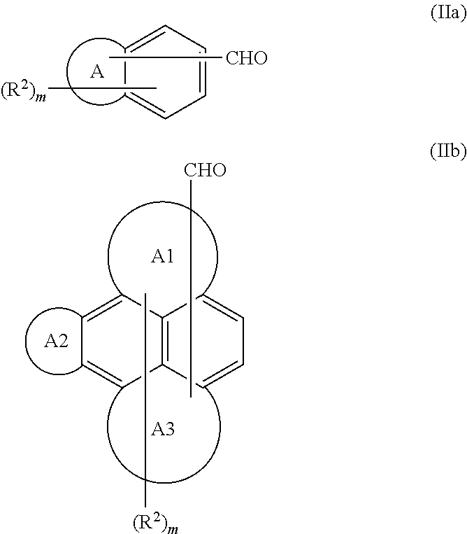
The aromatic aldehyde useful as the second monomer has the formula Ar—CHO, where Ar is a C10-C30aromatic moiety having at least 2 fused aromatic rings, which may optionally be substituted with one or more of C1-C30alkyl, C2-C30alkenyl, C7-C30aralkyl, C6-C30aryl, substituted C6-C30aryl, —OR2, —C1-C30alkylene-OR3, and —C1-C30alkylidene-OR3; R3 is selected from H, C1-C30alkyl, and C6-C30aryl. Preferably, Ar is a C10-C30aromatic moiety having from 2 to 5 fused aromatic rings, more preferably from 2 to 4 fused aromatic rings, and yet more preferably Ar is naphthyl. It is preferred that the C10-C30aromatic moiety of Ar is unsubstituted or substituted with one or more hydroxyls. Preferably, the aromatic aldehydes useful as the second monomer have the formula (IIa) or (IIb)
wherein A represents 1 to 4 fused aromatic rings; A1 represents 1 to 3 fused aromatic rings; each of A2 and A3 may be present or absent and each of A2 and A3 represents 1 to 2 fused aromatic rings; each R2 is independently selected from C1-C30alkyl, C2-C30alkenyl, C7-C30aralkyl, C6-C30aryl, substituted C6-C30aryl, —OR3, —C1-C30alkylene-OR3; each R3 is selected from H, C1-C30alkyl, and C6-C30aryl; and m is an integer from 0 to 13; wherein A1, A2 and A3 represent a total of 3 fused aromatic rings. It is preferred that A represents 1 to 3 aromatic rings, and more preferably 1 to 2 fused aromatic rings, and most preferably 1 fused aromatic ring. Preferably, A1 represents 1 or 2 fused aromatic rings. More preferably, each of A1 and A3 represent 1 fused aromatic ring. In another preferred aromatic aldehyde, each of A1, A2 and A3 represent 1 fused aromatic ring. Preferably, each R2 is independently selected from C1-C20alkyl, C2-C20alkenyl, C7-C30aralkyl, C6-C20aryl, —OR3, —C1-C20alkylene-OR3, and —C1-C20alkylidene-OR3; and more preferably from C1-C10alkyl, C2-C12alkenyl, C7-C30aralkyl, C6-C20aryl, —OR3, —C1-C20alkylene-OR3, and —C1-C20alkylidene-OR3. Preferably, R3 is selected from H, C1-C20alkyl, and C6-C20aryl, and more preferably H, C1-C10alkyl, and C6-C20aryl. Preferably, m is an integer from 0 to 10, more preferably from 0 to 8, still more preferably from 0 to 6, and yet more preferably from 0 to 5. Any of the fused aromatic rings in the structures of formulae (IIa) and (IIb) may be substituted with —CHO and/or one or more R2 moieties, and at least one of the fused aromatic rings in the structures of formulae (IIa) and (IIb) is substituted with —CHO. Mixtures of second monomers may be used.
The present reaction products are prepared by reacting one or more first monomers of formula (I) described above with one or more aromatic aldehydes of the formula Ar—CHO described above, in the presence of an acid catalyst, and optionally in a suitable solvent. The monomers and optional solvent may be combined in any order. Acid catalyst is typically added to the reaction mixture after the monomers and any optional solvent. Preferably, the reaction mixture is heated, such as from room temperature to 50° C. before addition of the acid catalyst. Following addition of the acid catalyst, the reaction mixture is typically heated, such as at reflux, for a period of time, such as from 1 to 48 hours. Following heating, the reaction product is isolated from the reaction mixture, such as by precipitation, and is typically dried, and optionally purified, before use. The molar ratio of total first monomer to total second monomer is from 1:0.75 to 2:1, and preferably from 1:1 to 1.5:1.
Reaction products of the invention may be prepared by the one or more first monomers and one or more second monomers without a solvent (neat) or preferably in the presence of a solvent. A variety of solvents may be used to prepare the present aromatic resin reaction products, such as, but not limited to, alcohols, glycol ethers, lactones, esters, water, and aromatic hydrocarbons. Preferably, a relatively polar solvent is used, such as alcohols, glycol ethers, lactones, esters or water. Mixtures of solvents may be used. It is preferred that at least one relatively polar solvent be used in the solvent mixture. Exemplary solvents include, without limitation, methanol, ethanol, propanol, propylene glycol, propylene glycol methyl ether, propylene glycol dimethyl ether, diethylene glycol dimethyl ether, propylene glycol methyl ether acetate (PGMEA), gamma-butyrolactone (GBL), gamma-valerolactone, delta-valerolactone, ethyl lactate, water, mesitylene, xylene, anisole, 4-methylanisole, and the like. Preferred solvents are methanol, ethanol, propanol, propylene glycol, propylene glycol methyl ether, propylene glycol dimethyl ether, propylene glycol methyl ether acetate, gamma-butyrolactone, gamma-valerolactone, delta-valerolactone, ethyl lactate, and water.
A variety of acids may suitably be used as catalysts in the preparation of the present aromatic resin reaction products. Such acids typically have a pKa of ≦2, preferably ≦1.5, more preferably ≦1, and yet more preferably ≦0. Exemplary acids include, without limitation, organic carboxylic acids and dicarboxylic acids such as propionic acid and oxalic acid, mineral acids and sulfonic acids, and preferably the acid catalysts is a mineral acid or a sulfonic acid. Suitable mineral acids are HF, HCl, HBr, HNO3, H2SO4, H3PO4, and HClO4. Suitable sulfonic acids include alkanesulfonic acids and arylsulfonic acids, such as methanesulfonic acid, ethanesulfonic acid, propanesulfonic acid, phenylsulfonic acid, phenolsulfonic acid, para-toluenesulfonic acid, and cresolsulfonic acid. Preferred acid catalysts are HCl, HBr, HNO3, H2SO4, H3PO4, methanesulfonic acid, ethanesulfonic acid, phenylsulfonic acid, phenolsulfonic acid, and para-toluenesulfonic acid (pTSA).
The aromatic resin reaction products of the invention typically have a weight average molecular weight (Mw) of 500 to 20000, preferably from 500 to 15000, and more preferably from 500 to 10000, as determined by gel permeation chromatography (GPC) using polystyrene standards.
When the first and second monomers described above are reacted in a relatively polar solvent, such as a mixture of propylene glycol methyl ether (PGME), ethanol and water, with a mineral acid, such as HCl, as the acid catalyst, the resulting aromatic resin reaction product possess a relatively polar moiety which is not present in the same reaction product prepared using a relatively non-polar solvent, such as an aromatic hydrocarbon. Such relatively polar moiety can be detected by HPLC (using an Agilent Zorbax Eclipse XDB-C8 column, liquid phase: 90/10 DI water/acetonitrile, followed by tetrahydrofuran) equipped with an evaporative light scattering detector. Such aromatic resin reaction products having such a relatively polar moiety show improved etch selectivity (that is, etch resistance) compared to the same reaction product prepared using a relatively non-polar solvent, such as an aromatic hydrocarbon.
A suitable composition useful for forming an underlayer comprises one or more aromatic resin reaction products described above, organic solvent, and optionally one or more additives chosen from curing agents, crosslinking agents, and surfactants. Mixtures of the present aromatic resin reaction products may be used in the present compositions. It will be appreciated by those skilled in the art that other additives may suitably be used in the present compositions. Any solvent may be used, provided that a sufficient amount of the aromatic resin reaction product is soluble in solvent, or solvent mixture, used. Such solvents include, but are not limited to, aromatic hydrocarbons, alcohols, lactones, esters, glycols, and glycol ethers. Mixtures of organic solvents may be used. Exemplary organic solvents include, without limitation, toluene, xylene, mesitylene, 2-methyl-1-butanol, 4-methyl-2-pentanol, methyl isobutyl carbinol, gamma-butyrolactone, ethyl lactate, methyl 2-hydroxyisobutyrate propylene glycol methyl ether acetate, propylene glycol methyl ether, and cyclohexanone. It will be appreciated by those skilled in the art that the concentration of the aromatic resin reaction products in the solvent may be varied across a wide range and that the thickness of any film deposited by a spin-on technique depends on the concentration of the reaction products in the solvent. Typically, the amount of aromatic resin in the composition is from 5 to 20 wt %, based on the total weight of the composition.
Optionally, the present aromatic resin compositions may further comprise one or more curing agents to aid in the curing of the deposited aromatic resin film. A curing agent is any component which causes curing of the aromatic resin film on the surface of a substrate. Preferred curing agents are thermal acid generators. A thermal acid generator is any compound which liberates acid upon exposure to heat. Thermal acid generators are well-known in the art and are generally commercially available, such as from King Industries, Norwalk, Conn. Exemplary thermal acid generators include, without limitation, amine blocked strong acids, such as amine blocked sulfonic acids such as amine blocked dodecylbenzenesulfonic acid. It will also be appreciated by those skilled in the art that certain photoacid generators are able to liberate acid upon heating and may function as thermal acid generators. The amount of such curing agents useful in the present compositions is well-known to those skilled in the art and is typically from 0 to 10 wt %, and preferably from 0 to 3 wt %.
Any suitable crosslinking agent may be used in the present compositions, provided that such crosslinking agent has at least 2, and preferably at least 3, moieties capable of reacting with the present aromatic resin reaction products under suitable conditions, such as under acidic conditions. Exemplary crosslinking agents include, but are not limited to, novolac resins, epoxy-containing compounds, melamine compounds, guanamine compounds, isocyanate-containing compounds, benzocyclobutenes, and the like, and preferably any of the foregoing having 2 or more, preferably 3 or more, and more preferably 4, substituents selected from methylol, C1-C10alkoxymethyl, and C2-C10acyloxymethyl. Examples of suitable crosslinking agents are those shown by formulae (III) and (IV).
Such crosslinking agents are well-known in the art, and are commercially available from a variety of sources. The amount of such crosslinking agents useful in the present compositions is well-known to those skilled in the art, and typically is in the range of 0 to 30 wt %, and preferably from 0 to 10 wt %.
The present aromatic resin compositions may optionally include one or more surface leveling agents (or surfactants). While any suitable surfactant may be used, such surfactants are typically non-ionic. Exemplary non-ionic surfactants are those containing an alkyleneoxy linkage, such as ethyleneoxy, propyleneoxy, or a combination of ethyleneoxy and propyleneoxy linkages. The amount of such surfactants useful in the present compositions is well-known to those skilled in the art, and typically is in the range of 0 to 5 wt %.
The present aromatic resin reaction products are useful in the manufacture of various electronic devices, such as in a process of forming a patterned layer comprising disposing a layer of the composition described above on a substrate; removing organic solvent to form a reaction product layer; disposing a layer of a photoresist on the reaction product layer; exposing the photoresist layer to actinic radiation through a mask; developing the exposed photoresist layer to form a resist pattern; and transferring the pattern to the reaction product layer to expose portions of the substrate.
The present compositions may be disposed on an electronic device substrate by any suitable means, such as spin-coating, slot-die coating, doctor blading, curtain coating, roller coating, spray coating, dip coating, and the like. Spin-coating is preferred. In a typical spin-coating method, the present compositions are applied to a substrate which is spinning at a rate of 500 to 4000 rpm for a period of 15-90 seconds to obtain a desired layer of the aromatic resin reaction product on the substrate. It will be appreciated by those skilled in the art that the height of the aromatic resin layer may be adjusted by changing the spin speed.
A wide variety of electronic device substrates may be used in the present invention, such as: packaging substrates such as multichip modules; flat panel display substrates; integrated circuit substrates; substrates for light emitting diodes (LEDs) including organic light emitting diodes (OLEDs); semiconductor wafers; polycrystalline silicon substrates; and the like. Such substrates are typically composed of one or more of silicon, polysilicon, silicon oxide, silicon nitride, silicon oxynitride, silicon germanium, gallium arsenide, aluminum, sapphire, tungsten, titanium, titanium-tungsten, nickel, copper, and gold. Suitable substrates may be in the form of wafers such as those used in the manufacture of integrated circuits, optical sensors, flat panel displays, integrated optical circuits, and LEDs. As used herein, the term “semiconductor wafer” is intended to encompass “an electronic device substrate,” “a semiconductor substrate,” “a semiconductor device,” and various packages for various levels of interconnection, including a single-chip wafer, multiple-chip wafer, packages for various levels, or other assemblies requiring solder connections. Such substrates may be any suitable size. Preferred wafer substrate diameters are 200 mm to 300 mm, although wafers having smaller and larger diameters may be suitably employed according to the present invention. As used herein, the term “semiconductive substrates” includes any substrate having one or more semiconductor layers or structures which include active or operable portions of semiconductor devices. The term “semiconductor substrate” is defined to mean any construction comprising semiconductive material, including but not limited to bulk semiconductive material such as a semiconductive wafer, either alone or in assemblies comprising other materials thereon, and semiconductive material layers, either alone or in assemblies comprising other materials. A semiconductor device refers to a semiconductor substrate upon which at least one microelectronic device has been or is being batch fabricated.
After being deposited on the substrate, the aromatic resin underlayer is optionally baked at a relatively low temperature to remove any solvent and other relatively volatile components from the underlayer. Typically, the substrate is baked at a temperature of ≦150° C., preferably from 60 to 125° C., and more preferably from 90 to 115° C. The baking time is typically from 10 seconds to 10 minutes, preferably from 30 seconds to 5 minutes, and more preferably from 6 to 90 seconds. When the substrate is a wafer, such baking step may be performed by heating the wafer on a hot plate.
The aromatic resin underlayer is then sufficiently cured such that the film does not intermix with a subsequently applied organic layer, such as a photoresist or other organic layer disposed directly on the underlayer. The aromatic resin underlayer may be cured in an oxygen-containing atmosphere, such as air, or in an inert atmosphere, such as nitrogen and under conditions, such as heating, sufficient to provide a cured aromatic resin underlayer. Such conditions are sufficient to cure the film such that it does not intermix with a subsequently applied organic layer, such as a photoresist layer, while still maintaining the desired antireflective properties (n and k values) and etch selectivity of the underlayer film. This curing step is conducted preferably on a hot plate-style apparatus, though oven curing may be used to obtain equivalent results. Typically, such curing is performed by heating the aromatic resin layer at a curing temperature of ≧150° C., and preferably 150 to 450° C. It is more preferred that the curing temperature is ≧200° C., still more preferably ≧250° C., and even more preferably from 250 to 400° C. The curing temperature selected should be sufficient for any thermal acid generator used to liberate acid to aid in curing of the aromatic resin. The curing time may be from 10 seconds to 10 minutes, preferably from 30 seconds to 5 minutes, more preferably from 45 seconds to 5 minutes, and yet more preferably from 45 to 90 seconds. The choice of final curing temperature depends mainly upon the desired curing rate, with higher curing temperatures requiring shorter curing times.
The initial baking step may not be necessary if the curing step is conducted in such a way that rapid evolution of the solvents and curing by-products is not allowed to disrupt the film quality. For example, a ramped bake beginning at relatively low temperatures and then gradually increasing to the range of 200 to 325° C. can give acceptable results. It can be preferable in some cases to have a two-stage curing process, with the first stage being a lower bake temperature of less than 200° C., and the second stage being a higher bake temperature preferably between 200 and 400° C. Two stage curing processes facilitate uniform filling and planarization of pre-existing substrate surface topography, for example filling of trenches and vias.
After curing of the aromatic resin underlayer, one or more processing layers, such as photoresists, silicon-containing layers, hardmask layers, bottom antireflective coating (or BARC) layers, and the like, may be disposed on the cured underlayer. For example, a photoresist may be disposed, such as by spin coating, directly on the surface of the cured aromatic resin underlayer. A wide variety of photoresists may be suitably used, such as those used in 193 nm lithography, such as those sold under the EPIC ™ brand available from Dow Electronic Materials (Marlborough, Mass.). Suitable photoresists may be either positive tone development or negative tone development resists. Following coating on the aromatic resin underlayer, the photoresist layer is then imaged (exposed) using patterned actinic radiation, and the exposed photoresist layer is then developed using the appropriate developer to provide a patterned photoresist layer. The pattern is next transferred from the photoresist layer to the underlayer by an appropriate etching technique. Typically, the photoresist is also removed during such etching step. Next, the pattern is transferred to the substrate and the underlayer removed by appropriate etching techniques known in the art, such as by plasma etching. Following patterning of the substrate, the underlayer is removed using conventional techniques. The electronic device substrate is then processed according to conventional means.
Alternatively, the cured aromatic resin underlayer may be used as the bottom layer of a multilayer resist process. In such a process, a layer of the aromatic resin reaction product is disposed on a substrate and cured as described above. Next, one or more middle layers are disposed on the aromatic resin underlayer. For example, a silicon-containing layer or a hardmask layer is disposed directly on the aromatic resin underlayer. Exemplary silicon-containing layers include a silicon-BARC, which may be spin coated on the underlayer followed by curing, or an inorganic silicon layer such as SiON or SiO2 which may be deposited on the underlayer by chemical vapor deposition (CVD). Any suitable hardmask may be used and may be deposited on the underlayer by any suitable technique, and cured as appropriate. Optionally, an organic BARC layer may be disposed directly on the silicon-containing layer or hardmask layer, and appropriately cured. Next, a photoresist, such as those used in 193 nm lithography, is disposed directly on the silicon-containing layer (in a trilayer process) or directly on the organic BARC layer (in a quadlayer process). The photoresist layer is then imaged (exposed) using patterned actinic radiation, and the exposed photoresist layer is then developed using the appropriate developer to provide a patterned photoresist layer. The pattern is next transferred from the photoresist layer to the layer directly below it, by appropriate etching techniques known in the art, such as by plasma etching, resulting in a patterned silicon-containing layer in a trilayer process and a patterned organic BARC layer in a quadlayer process. If a quadlayer process is used, the pattern is next transferred from the organic BARC layer to the silicon-containing layer or hardmask layer using appropriate pattern transfer techniques, such as plasma etching. After the silicon-containing layer or hardmask layer is patterned, the aromatic resin underlayer is then patterned using appropriate etching techniques, such as O2 plasma. Any remaining patterned photoresist and organic BARC layers are removed during etching of the aromatic resin underlayer. Next, the pattern is then transferred to the substrate, such as by appropriate etching techniques, which also removes any remaining silicon-containing layer or hardmask layer, followed by removal of any remaining patterned aromatic resin underlayer to provide a patterned substrate.
Aromatic reaction products of the invention may also be used in a self-aligned double patterning process. In such a process, a layer of an aromatic resin reaction product described above is disposed on a substrate, such as by spin-coating. Any remaining organic is removed and the aromatic resin layer is cured to form an aromatic resin underlayer. A layer of a suitable photoresist is then disposed on the cured aromatic resin underlayer, such as by spin coating. The photoresist layer is then imaged (exposed) using patterned actinic radiation, and the exposed photoresist layer is then developed using the appropriate developer to provide a patterned photoresist layer. The pattern is next transferred from the photoresist layer to the aromatic resin underlayer by an appropriate etching technique to expose portions of the substrate. Typically, the photoresist is also removed during such etching step. Next, a conformal silicon-containing layer is disposed over the patterned polymeric reaction product layer and exposed portions of the substrate. Such silicon-containing layer is typically an inorganic silicon layer such as SiON or SiO2 which is conventionally deposited by CVD. Such conformal coatings result in a silicon-containing layer on the exposed portions of the substrate surface as well as over the underlayer pattern, that is, such silicon-containing layer substantially covers the sides and top of the underlayer pattern. Next, the silicon-containing layer is partially etched (trimmed) to expose a top surface of the patterned aromatic resin underlayer and a portion of the substrate. Following this partial etching step, the pattern on the substrate comprises a plurality of features, each feature comprising a line or post of the aromatic resin underlayer with the silicon-containing layer directly adjacent to the sides of each aromatic resin underlayer feature. Next, the aromatic resin underlayer is removed, such as by etching, to expose the substrate surface that was under the aromatic resin underlayer pattern, and providing a patterned silicon-containing layer on the substrate surface, where such patterned silicon-containing layer is doubled (that is, twice as many lines and/or posts) as compared to the patterned aromatic resin underlayer.
The present aromatic resin reaction products provide underlayers having improved etch resistance to oxygen and fluorine gases, high carbon content, reduced or no swelling from exposure to processing fluids, and very good planarization and gap filling properties, making such reaction products useful in a variety of semiconductor manufacturing processes.
A three-necked 50 mL round-bottom flask was equipped with a mechanical stirrer, a thermowell, and a condenser with a nitrogen inlet. The flask was charged with 1-pyrenol (5.0 g, 0.0229 mol), 2-naphthaldehyde (3.578 g, 0.0229 mol), and PGME (10 mL) and EtOH (7 mL). Stirring was then initiated and the reaction mixture was heated to 60° C. under nitrogen. A clear solution was obtained after 30 minutes and heating was removed at that time. HCl (3.0 mL, 37% in water) was added dropwise to the reaction mixture at 40° C. The reaction mixture was refluxed for 24 hours to give a thick, dark brown solution. The reaction mixture was cooled to room temperature and diluted with 10 mL PGME. The mixture was then added to 250 mL methanol to give a light grey precipitate. The precipitated resin was filtered, vacuum dried at 60 to 70° C. to give 4.3 g resin (Sample 1) as grey powder. Analysis by GPC: Mw=2321, polydispersity index (PDI)=1.24.
The procedure of Example 1 was repeated and analysis of the resulting resin (Sample 2) by GPC provided the following: Mw=2231, PDI=1.33.
A three-necked 50 mL round-bottom flask was equipped with a mechanical stirrer, a thermowell, and a condenser with a nitrogen inlet. The flask was charged with 1-pyrenol (4.0 g, 0.0183 mol), 2-naphthaldehyde (2.8624 g, 0.0183 mol), and toluene (24 mL). Stirring was then initiated and the reaction mixture was heated to 60° C. under nitrogen. A clear solution was obtained after 30 minutes and heating was removed at that time. Methanesulfonic acid (1.76 g, 0.0183 mol) was added dropwise to the reaction mixture at 40° C. The reaction mixture was heated at 100 to 110° C. for 12 hours to give a thick solution. The reaction mixture was then cooled to room temperature. The mixture was added to 250 mL methanol to give a grey precipitate. The precipitated resin was filtered, vacuum dried at 60 to 70° C. to give 3.6 g resin (Sample 3) as grey powder. Analysis by GPC: Mw=2697, PDI=1.6.
The procedure of Example 1 was generally repeated except that the solvents and acids shown in Table 1 were used.
TABLE 1 | ||||||
Sample | Solvent | Acid | Mw | PDI | ||
4-1 | PGMEA | CH3SO3H | 5012 | 2.2 | ||
4-2 | GBL | CH3SO3H | 2910 | 1.53 | ||
The procedure of Example 1 is repeated except that 2-naphthaldehyde is replaced with the aldehydes listed in Table 2.
TABLE 2 | |||
Sample | Aldehyde | Solvent | Acid |
5-1 | Anthracene-2-carbaldehyde | GBL | CH3SO3H |
5-2 | Pyrene-1-carbaldehyde | EtOH/PGME | HCl |
5-3 | 6-Hydroxyanthracene-6- | EtOH/PGME | H2SO4 |
carbaldehyde | |||
5-4 | Phenanthrene-2-carbaldehyde | GBL | CH3SO3H |
5-5 | 6-Hydroxy-2-naphthaldehyde | EtOH/PGME | HCl |
5-6 | 5-Hydroxy-2-naphthaldehyde | EtOH/PGME | HCl |
5-7 | 6-Hydroxypyrene-1-carbaldehyde | EtOH/PGME | HCl |
5-8 | Triphenylene-2-carbaldehyde | GBL | CH3SO3H |
5-9 | 5-Hydroxyanthracene-6- | EtOH/PGME | H2SO4 |
carbaldehyde | |||
5-10 | Anthracene-9-carbaldehyde | GBL | CH3SO3H |
5-11 | 3-Hydroxyanthracene-9- | EtOH/PGME | HCl |
carbaldehyde | |||
5-12 | 2-Hydroxy-3-naphthaldehyde | EtOH/PGME | Propionic acid |
5-12 | 2-Methoxy-1-naphthaldehyde | GBL | CH3SO3H |
5-13 | 2-Benzyloxy-1-naphthaldehyde | GBL | CH3SO3H |
5-14 | 9-Phenylanthracene-2- | GBL | CH3SO3H |
carbaldehyde | |||
5-15 | 9-Hydroxytriphenylene-2- | EtOH/PGME | H2SO4 |
carbaldehyde | |||
5-16 | 5-Phenyl-2-naphthaldehyde | GBL | CH3SO3H |
5-17 | 5-Phenyl-2-naphthaldehyde | 4-methylanisole | pTSA |
A three-necked 50 mL round-bottom flask was equipped with a mechanical stirrer, a thermowell, and a condenser with a nitrogen inlet. The flask was charged with 1-pyrenol (10.0 g, 0.0458 mol), 2-naphthaldehyde (7.156 g, 0.0458 mol), and PGME (40 mL). Stirring was then initiated and the reaction mixture was stirred at room temperature under nitrogen. A clear solution was obtained after 30 minutes. Methanesulfonic acid (2.201 g, 0.0229 mol) was added to the reaction mixture. The reaction mixture was heated at 120° C. for 4 hours to give a thick solution. The reaction mixture was then cooled to room temperature. The mixture was added to 400 mL methanol and water (v/v=4:1) to give a grey precipitate. The precipitated resin was filtered, vacuum dried at 60 to 70° C. to give 11.3 g resin as grey powder (Sample 6). Analysis by GPC: Mw=1229, PDI=1.2.
The procedure of Example 6 was repeated except that the 1-pyrenol loading and reaction times used were as shown in Table 3.
TABLE 3 | ||||
Sample | 1-Pyrenol | Time | Mw | PDI |
7-1 | 1.5 equivalents | 11 hr. | 1150 | 1.15 |
7-2 | 2 equivalents | 11 hr. | 1000 | 1.13 |
A three-necked 50 mL round-bottom flask was equipped with a mechanical stirrer, a thermowell, and a condenser with a nitrogen inlet. The flask was charged with 1-pyrenol (5.0 g, 0.0229 mol), benzaldehyde (2.431 g, 0.0229 mol), PGME (10 mL) and EtOH (7 mL). Stirring was then initiated and the reaction mixture was heated to 60° C. under nitrogen. A clear solution was obtained after 30 minutes and heating was removed at that time. HCl (3.0 mL, 37% aqueous) was added dropwise to the reaction mixture at 40° C. The reaction mixture was refluxed for 24 hours to give a thick, dark brown solution. The reaction mixture was cooled to room temperature and diluted with 10 mL PGME. The mixture was then added to 500 mL methanol to give a light grey precipitate. The precipitated resin was filtered, vacuum dried at 60 to 70° C. to give 1.0 g resin (Comparative 1) as grey powder. Analysis by GPC: Mw=4526, PDI=1.88.
A sample (Comparative 2) of a polymer having the repeating unit shown in formula (V) was obtained from Gun Ei Chemical, and used as is. The molecular weight of this sample was: Mw=6066, and Mn=2362.
The aromatic resin reaction products listed in Table 5 were individually formulated in propyleneglycol monomethylether acetate (PGMEA) or cyclohexanone at 10 wt % solids, filtered through 0.2 μm poly(tetrafluoroethylene) (PTFE) syringe filter, coated on a silicon wafer at 1500 rpm and baked at 100° C. for 60 seconds to remove the solvent, and further cured at 400° C. for 60 seconds. The cured films were etched using either O2 or CF4 plasma using a Plasmatherm RIE790 tool (from Plasma-Therm Co.) and the conditions shown in Table 4. The etching data, in Å/sec., are reported in Table 5.
TABLE 4 | ||
Gas | O2 | CF4 |
Flow (sccm) | 60 | 50 |
Power (W) | 700 | 500 |
Pressure (mTorr) | 10 | 10 |
Etch time (sec.) | 30 | 60 |
TABLE 5 | ||
Sample | O2 Etch-Å/sec. | CF4 Etch-Å/sec. |
2 | 23.5 | 3.0 |
4-1 | 26.4 | 3.2 |
4-2 | 27.2 | 5.6 |
6 | 23.2 | 5.1 |
7-1 | 22.4 | 3.7 |
7-2 | 21.9 | 2.6 |
Comparative 1 | 28.2 | 4.1 |
Comparative 2 | 31.6 | 5.0 |
Claims (13)
1. A reaction product formed from a combination comprising one or more first monomers of the formula
wherein Y is selected from H, C1-C30alkyl, C2-C30alkenyl, C7-C30aralkyl, C6-C30aryl, substituted C6-C30aryl, —C1-C30alkylene-OR1, and —C1-C30alkylidene-OR1; each R is independently selected from C1-C30alkyl, C2-C30alkenyl, C7-C30aralkyl, C6-C30aryl, substituted C6-C30aryl, —OR1, —C1-C30alkylene-OR1, and —C1-C30alkylidene-OR1; R1 is selected from H, C1-C30alkyl, C6-C30aryl, substituted C6-C30aryl, and C7-C30aralkyl; and n is an integer selected from 0 to 7; and one or more second monomers of formula (IIa) or (IIb)
wherein A represents 1 to 4 fused aromatic rings; A1 represents 1 to 3 fused aromatic rings; each of A2 and A3 may be present or absent and each of A2 and A3 represents 1 to 2 fused aromatic rings; each R2 is independently selected from C1-C30alkyl, C2-C30alkenyl, C7-C30aralkyl, C6-C30aryl, substituted C6-C30aryl, —OR3, —C1-C30alkylene-OR3; each R3 is selected from H, C1-C30alkyl, and C6-C30aryl; and m is an integer from 0 to 13; wherein A1, A2 and A3 represent a total of 3 fused aromatic rings.
2. The reaction product of claim 1 wherein n=0 to 4.
3. The reaction product of claim 1 wherein each R is independently selected from C1-C20alkyl, C2-C20alkenyl, C7-C30aralkyl, C6-C30aryl, substituted —C6-C30aryl, —OR1, —C1-C12alkylene-OR1, and —C1-C20alkylidene-OR1.
4. The reaction product of claim 1 wherein each R is independently selected from hydroxyl, methyl, ethyl, propyl, iso-butyl, tert-butyl, cyclopentyl, cyclohexyl, cyclopentenylmethyl, cyclohexenylmethyl, 2-cyclohexenylmeth-1-yl, methoxy, ethoxy, propyloxy, phenyl, tolyl, xylyl, naphthyl, biphenyl, benzyl, phenethyl, naphthylmethyl, pyerenylmethyl, antracenylmethyl, methoxy, ethoxy, propyloxy, phenyloxy, naphthyloxy, benzyloxy, phenethyloxy, methoxymethyl, methoxyethyl, methoxyphenyl, and methoxynaphthyl.
5. The reaction product of claim 1 wherein second monomer is substituted with one or more hydroxyls.
6. A process for preparing a reaction product comprising reacting one or more first monomers of the formula
wherein Y is selected from H, C1-C30alkyl, C2-C30alkenyl, C7-C30aralkyl, C6-C30aryl, substituted C6-C30aryl, —C1-C30alkylene-OR1, and —C1-C30alkylidene-OR1; each R is independently selected from C1-C30alkyl, C2-C30alkenyl, C7-C30aralkyl, C6-C30aryl, substituted C6-C30aryl, —OR1, —C1-C30alkylene-OR1, and —C1-C30alkylidene-OR1; R1 is selected from H, C1-C30alkyl, C6-C30aryl, substituted C6-C30aryl, and C7-C30aralkyl; and n is an integer selected from 0 to 7; with one or more second monomers of formula (IIa) or (IIb)
wherein A represents 1 to 4 fused aromatic rings; A1 represents 1 to 3 fused aromatic rings; each of A2 and A3 may be present or absent and each of A2 and A3 represents 1 to 2 fused aromatic rings; each R2 is independently selected from C1-C30alkyl, C2-C30alkenyl, C7-C30aralkyl, C6-C30aryl, substituted C6-C30aryl, —OR3, —C1-C30alkylene-OR3; each R3 is selected from H, C1-C30alkyl, and C6-C30aryl; and m is an integer from 0 to 13; wherein A1, A2 and A3 represent a total of 3 fused aromatic rings in the presence of an acid, and optionally in a solvent.
7. The process of claim 6 wherein the solvent is polar.
8. The process of claim 6 wherein the acid is selected from dicarboxylic acids, mineral acids and sulfonic acids.
9. A polymeric reaction product produced by the process of claim 6 .
10. A composition comprising the reaction product of claim 1 , organic solvent, and optionally one or more additives chosen from curing agents, crosslinking agents, and surfactants.
11. A process of forming a patterned layer comprising disposing a layer of the composition of claim 10 on a substrate; removing organic solvent to form a reaction product layer; disposing a layer of a photoresist on the reaction product layer; exposing the photoresist layer to actinic radiation through a mask; developing the exposed photoresist layer to form a resist pattern; and transferring the pattern to the reaction product layer to expose portions of the substrate.
12. The process of claim 11 further comprising the steps of patterning the substrate; and then removing the patterned reaction product layer.
13. The process of claim 11 further comprising the steps of disposing a conformal silicon-containing layer over the patterned reaction product layer and exposed portions of the substrate; partially etching the silicon-containing layer to expose a top surface of the patterned polymeric reaction product layer and a portion of the substrate.
Priority Applications (1)
Application Number | Priority Date | Filing Date | Title |
---|---|---|---|
US15/363,114 US9809672B2 (en) | 2013-12-12 | 2016-11-29 | Aromatic resins for underlayers |
Applications Claiming Priority (3)
Application Number | Priority Date | Filing Date | Title |
---|---|---|---|
US201361915475P | 2013-12-12 | 2013-12-12 | |
US14/569,610 US9540476B2 (en) | 2013-12-12 | 2014-12-12 | Aromatic resins for underlayers |
US15/363,114 US9809672B2 (en) | 2013-12-12 | 2016-11-29 | Aromatic resins for underlayers |
Related Parent Applications (1)
Application Number | Title | Priority Date | Filing Date |
---|---|---|---|
US14/569,610 Continuation US9540476B2 (en) | 2013-12-12 | 2014-12-12 | Aromatic resins for underlayers |
Publications (2)
Publication Number | Publication Date |
---|---|
US20170073453A1 US20170073453A1 (en) | 2017-03-16 |
US9809672B2 true US9809672B2 (en) | 2017-11-07 |
Family
ID=53367635
Family Applications (2)
Application Number | Title | Priority Date | Filing Date |
---|---|---|---|
US14/569,610 Active US9540476B2 (en) | 2013-12-12 | 2014-12-12 | Aromatic resins for underlayers |
US15/363,114 Active US9809672B2 (en) | 2013-12-12 | 2016-11-29 | Aromatic resins for underlayers |
Family Applications Before (1)
Application Number | Title | Priority Date | Filing Date |
---|---|---|---|
US14/569,610 Active US9540476B2 (en) | 2013-12-12 | 2014-12-12 | Aromatic resins for underlayers |
Country Status (5)
Country | Link |
---|---|
US (2) | US9540476B2 (en) |
JP (1) | JP6525373B2 (en) |
KR (1) | KR102313101B1 (en) |
CN (1) | CN104710588B (en) |
TW (1) | TWI542614B (en) |
Families Citing this family (19)
Publication number | Priority date | Publication date | Assignee | Title |
---|---|---|---|---|
JP6445382B2 (en) * | 2015-04-24 | 2018-12-26 | 信越化学工業株式会社 | Method for producing composition for forming coating film for lithography and method for forming pattern |
KR101940655B1 (en) * | 2016-11-22 | 2019-01-21 | 동우 화인켐 주식회사 | Composition for hard mask |
US11175581B2 (en) * | 2016-12-05 | 2021-11-16 | Rohm And Haas Electronic Materials Llc | Aromatic resins for underlayers |
US10790146B2 (en) * | 2016-12-05 | 2020-09-29 | Rohm And Haas Electronic Materials Llc | Aromatic resins for underlayers |
CN106946677B (en) * | 2017-04-20 | 2019-07-12 | 深圳市华星光电半导体显示技术有限公司 | Fused ring compound and its application, electroluminescent device and preparation method thereof |
KR102349952B1 (en) * | 2018-01-17 | 2022-01-10 | 동우 화인켐 주식회사 | Composition for hard mask |
US10804106B2 (en) * | 2018-02-21 | 2020-10-13 | International Business Machines Corporation | High temperature ultra-fast annealed soft mask for semiconductor devices |
KR102287506B1 (en) | 2018-07-11 | 2021-08-09 | 삼성에스디아이 주식회사 | Hardmask composition, hardmask layer and method of forming patterns |
KR102244470B1 (en) | 2018-07-18 | 2021-04-23 | 삼성에스디아이 주식회사 | Polymer, organic layer composition and method of forming patterns |
JP6981945B2 (en) | 2018-09-13 | 2021-12-17 | 信越化学工業株式会社 | Pattern formation method |
KR102397179B1 (en) | 2018-12-21 | 2022-05-11 | 삼성에스디아이 주식회사 | Hardmask composition, hardmask layer and method of forming patterns |
KR102260811B1 (en) | 2018-12-26 | 2021-06-03 | 삼성에스디아이 주식회사 | Hardmask composition, hardmask layer and method of forming patterns |
TWI843893B (en) * | 2019-10-09 | 2024-06-01 | 日商日產化學股份有限公司 | Resist underlayer film forming composition |
TW202204298A (en) * | 2020-05-02 | 2022-02-01 | 美商羅門哈斯電子材料有限公司 | Aromatic underlayer |
US11940732B2 (en) * | 2020-05-02 | 2024-03-26 | Rohm And Haas Electronic Materials Llc | Coating compositions and methods of forming electronic devices |
US11762294B2 (en) | 2020-08-31 | 2023-09-19 | Rohm And Haas Electronic Materials Llc | Coating composition for photoresist underlayer |
KR20220138243A (en) * | 2021-04-05 | 2022-10-12 | 삼성에스디아이 주식회사 | Hardmask composition, hardmask layer and method of forming patterns |
KR20230108593A (en) * | 2022-01-11 | 2023-07-18 | 삼성에스디아이 주식회사 | Hardmask composition, hardmask layer and method of forming patterns |
JP2024116011A (en) | 2023-02-15 | 2024-08-27 | 信越化学工業株式会社 | Pattern Formation Method |
Citations (16)
Publication number | Priority date | Publication date | Assignee | Title |
---|---|---|---|---|
CN1550898A (en) | 2003-05-19 | 2004-12-01 | 东京应化工业株式会社 | Positive anticorrosive additive composition and anticorrosive pattern forming method |
US20080153033A1 (en) | 2006-12-20 | 2008-06-26 | Kyung Hee Hyung | Polymer having antireflective properties, hardmask composition including the same, process for forming a patterned material layer, and associated device |
US20090098486A1 (en) | 2006-03-14 | 2009-04-16 | Jsr Corporation | Composition for forming lower layer film and pattern forming method |
US20100021830A1 (en) | 2007-04-02 | 2010-01-28 | Min Soo Kim | Aromatic ring-containing polymer, polymer mixture, antireflective hardmask composition, and associated methods |
US20100055373A1 (en) | 2007-04-25 | 2010-03-04 | Nexolve Corporation | Polymer seaming with diffusion welds |
KR20100080139A (en) | 2008-12-31 | 2010-07-08 | 제일모직주식회사 | High etch resistant polymer having high carbon with aromatic rings, composition containing the same, and method of patterning materials using the same |
US7816067B2 (en) | 2005-06-10 | 2010-10-19 | Nissan Chemical Industries, Ltd. | Coating-type underlayer coating forming composition for lithography containing naphthalene resin derivative |
US7862990B2 (en) | 2006-12-30 | 2011-01-04 | Cheil Industries, Inc. | Polymer having antireflective properties and high carbon content, hardmask composition including the same, and process for forming a patterned material layer |
US20110117501A1 (en) * | 2009-11-13 | 2011-05-19 | Jee Yun Song | Resist underlayer polymer, resist underlayer composition including the same, and method of patterning using the same |
US20120064725A1 (en) | 2010-09-10 | 2012-03-15 | Shin-Etsu Chemical Co., Ltd. | Naphthalene derivative, resist bottom layer material, and patterning process |
US20120171611A1 (en) | 2009-09-15 | 2012-07-05 | Ryuji Ideno | Aromatic hydrocarbon resin and composition for forming underlayer film for lithography |
US20130171569A1 (en) | 2012-01-04 | 2013-07-04 | Shin-Etsu Chemical Co., Ltd. | Resist underlayer film composition, method for producing polymer for resist underlayer film, and patterning process using the resist underlayer film composition |
US20130189533A1 (en) | 2010-10-14 | 2013-07-25 | Nissan Chemical Industries, Ltd. | Resist underlayer film forming composition for lithography containing polyether structure-containing resin |
US8778592B2 (en) | 2011-02-25 | 2014-07-15 | Shin-Etsu Chemical Co., Ltd. | Positive resist composition and patterning process |
US20150011092A1 (en) | 2012-02-01 | 2015-01-08 | Nissan Chemical Industries, Ltd. | Resist underlayer film-forming composition containing copolymer resin having heterocyclic ring |
US20150044876A1 (en) | 2012-03-27 | 2015-02-12 | Nissan Chemical Industries, Ltd. | Resist underlayer film forming composition containing phenylindole-containing novolac resin |
Family Cites Families (6)
Publication number | Priority date | Publication date | Assignee | Title |
---|---|---|---|---|
EP1762895B1 (en) * | 2005-08-29 | 2016-02-24 | Rohm and Haas Electronic Materials, L.L.C. | Antireflective Hard Mask Compositions |
KR100908601B1 (en) * | 2007-06-05 | 2009-07-21 | 제일모직주식회사 | Anti-reflective hard mask composition and patterning method of substrate material using same |
US20100119980A1 (en) * | 2008-11-13 | 2010-05-13 | Rahman M Dalil | Antireflective Coating Composition Comprising Fused Aromatic Rings |
JP5257009B2 (en) * | 2008-11-14 | 2013-08-07 | Jsr株式会社 | Resist underlayer film forming composition, resist underlayer film forming method, and pattern forming method |
US8501383B2 (en) * | 2009-05-20 | 2013-08-06 | Rohm And Haas Electronic Materials Llc | Coating compositions for use with an overcoated photoresist |
EP2716671B1 (en) * | 2011-06-03 | 2018-10-10 | Mitsubishi Gas Chemical Company, Inc. | Phenolic resin and material for forming underlayer film for lithography |
-
2014
- 2014-12-12 US US14/569,610 patent/US9540476B2/en active Active
- 2014-12-12 TW TW103143446A patent/TWI542614B/en active
- 2014-12-12 JP JP2014251549A patent/JP6525373B2/en active Active
- 2014-12-12 CN CN201410858338.0A patent/CN104710588B/en active Active
- 2014-12-12 KR KR1020140179777A patent/KR102313101B1/en active IP Right Grant
-
2016
- 2016-11-29 US US15/363,114 patent/US9809672B2/en active Active
Patent Citations (19)
Publication number | Priority date | Publication date | Assignee | Title |
---|---|---|---|---|
CN1550898A (en) | 2003-05-19 | 2004-12-01 | 东京应化工业株式会社 | Positive anticorrosive additive composition and anticorrosive pattern forming method |
US7816067B2 (en) | 2005-06-10 | 2010-10-19 | Nissan Chemical Industries, Ltd. | Coating-type underlayer coating forming composition for lithography containing naphthalene resin derivative |
US20090098486A1 (en) | 2006-03-14 | 2009-04-16 | Jsr Corporation | Composition for forming lower layer film and pattern forming method |
US20080153033A1 (en) | 2006-12-20 | 2008-06-26 | Kyung Hee Hyung | Polymer having antireflective properties, hardmask composition including the same, process for forming a patterned material layer, and associated device |
US7862990B2 (en) | 2006-12-30 | 2011-01-04 | Cheil Industries, Inc. | Polymer having antireflective properties and high carbon content, hardmask composition including the same, and process for forming a patterned material layer |
US20100021830A1 (en) | 2007-04-02 | 2010-01-28 | Min Soo Kim | Aromatic ring-containing polymer, polymer mixture, antireflective hardmask composition, and associated methods |
US20100055373A1 (en) | 2007-04-25 | 2010-03-04 | Nexolve Corporation | Polymer seaming with diffusion welds |
KR20100080139A (en) | 2008-12-31 | 2010-07-08 | 제일모직주식회사 | High etch resistant polymer having high carbon with aromatic rings, composition containing the same, and method of patterning materials using the same |
KR101257697B1 (en) | 2008-12-31 | 2013-04-24 | 제일모직주식회사 | High etch resistant polymer having high carbon with aromatic rings, composition containing the same, and method of patterning materials using the same |
US20120171611A1 (en) | 2009-09-15 | 2012-07-05 | Ryuji Ideno | Aromatic hydrocarbon resin and composition for forming underlayer film for lithography |
US20110117501A1 (en) * | 2009-11-13 | 2011-05-19 | Jee Yun Song | Resist underlayer polymer, resist underlayer composition including the same, and method of patterning using the same |
US20120064725A1 (en) | 2010-09-10 | 2012-03-15 | Shin-Etsu Chemical Co., Ltd. | Naphthalene derivative, resist bottom layer material, and patterning process |
US20130189533A1 (en) | 2010-10-14 | 2013-07-25 | Nissan Chemical Industries, Ltd. | Resist underlayer film forming composition for lithography containing polyether structure-containing resin |
US8778592B2 (en) | 2011-02-25 | 2014-07-15 | Shin-Etsu Chemical Co., Ltd. | Positive resist composition and patterning process |
US20130171569A1 (en) | 2012-01-04 | 2013-07-04 | Shin-Etsu Chemical Co., Ltd. | Resist underlayer film composition, method for producing polymer for resist underlayer film, and patterning process using the resist underlayer film composition |
US20150011092A1 (en) | 2012-02-01 | 2015-01-08 | Nissan Chemical Industries, Ltd. | Resist underlayer film-forming composition containing copolymer resin having heterocyclic ring |
US9261790B2 (en) | 2012-02-01 | 2016-02-16 | Nissan Chemical Industries, Ltd. | Resist underlayer film-forming composition containing copolymer resin having heterocyclic ring |
US20150044876A1 (en) | 2012-03-27 | 2015-02-12 | Nissan Chemical Industries, Ltd. | Resist underlayer film forming composition containing phenylindole-containing novolac resin |
US8993215B2 (en) | 2012-03-27 | 2015-03-31 | Nissan Chemical Industries, Ltd. | Resist underlayer film forming composition containing phenylindole-containing novolac resin |
Non-Patent Citations (2)
Title |
---|
Search report for corresponding China Application No. 201410858338.0 dated May 24, 2016. |
Search report for corresponding Taiwan Application No. 103143446 dated Oct. 7, 2015. |
Also Published As
Publication number | Publication date |
---|---|
US20150166711A1 (en) | 2015-06-18 |
CN104710588A (en) | 2015-06-17 |
JP6525373B2 (en) | 2019-06-05 |
JP2015131954A (en) | 2015-07-23 |
US9540476B2 (en) | 2017-01-10 |
US20170073453A1 (en) | 2017-03-16 |
KR102313101B1 (en) | 2021-10-15 |
CN104710588B (en) | 2017-04-12 |
TW201538577A (en) | 2015-10-16 |
KR20150069557A (en) | 2015-06-23 |
TWI542614B (en) | 2016-07-21 |
Similar Documents
Publication | Publication Date | Title |
---|---|---|
US9809672B2 (en) | Aromatic resins for underlayers | |
US10377848B2 (en) | Aromatic resins for underlayers | |
CN110837205B (en) | Aromatic bottom layer | |
US10790146B2 (en) | Aromatic resins for underlayers | |
US9880469B2 (en) | Resins for underlayers | |
US9601325B2 (en) | Aromatic resins for underlayers | |
JP7386219B2 (en) | aromatic lower layer | |
US11940732B2 (en) | Coating compositions and methods of forming electronic devices | |
CN118276403A (en) | Photoresist underlayer composition and method of forming electronic device | |
US20210343522A1 (en) | Coating compositions and methods of forming electronic devices | |
CN117447900A (en) | Coating composition for photoresist underlayer | |
TW202204298A (en) | Aromatic underlayer |
Legal Events
Date | Code | Title | Description |
---|---|---|---|
STCF | Information on status: patent grant |
Free format text: PATENTED CASE |
|
AS | Assignment |
Owner name: ROHM AND HAAS ELECTRONIC MATERIALS LLC, MASSACHUSE Free format text: ASSIGNMENT OF ASSIGNORS INTEREST;ASSIGNORS:CUI, LI;CHO, SUNG WOOK;LI, MINGQI;AND OTHERS;SIGNING DATES FROM 20141001 TO 20141008;REEL/FRAME:045044/0362 |
|
MAFP | Maintenance fee payment |
Free format text: PAYMENT OF MAINTENANCE FEE, 4TH YEAR, LARGE ENTITY (ORIGINAL EVENT CODE: M1551); ENTITY STATUS OF PATENT OWNER: LARGE ENTITY Year of fee payment: 4 |