US9805872B2 - Multiple MLCC modules - Google Patents
Multiple MLCC modules Download PDFInfo
- Publication number
- US9805872B2 US9805872B2 US14/963,766 US201514963766A US9805872B2 US 9805872 B2 US9805872 B2 US 9805872B2 US 201514963766 A US201514963766 A US 201514963766A US 9805872 B2 US9805872 B2 US 9805872B2
- Authority
- US
- United States
- Prior art keywords
- module
- lead
- forming
- interconnect
- longitudinal edge
- Prior art date
- Legal status (The legal status is an assumption and is not a legal conclusion. Google has not performed a legal analysis and makes no representation as to the accuracy of the status listed.)
- Active, expires
Links
Images


Classifications
-
- H—ELECTRICITY
- H01—ELECTRIC ELEMENTS
- H01G—CAPACITORS; CAPACITORS, RECTIFIERS, DETECTORS, SWITCHING DEVICES, LIGHT-SENSITIVE OR TEMPERATURE-SENSITIVE DEVICES OF THE ELECTROLYTIC TYPE
- H01G4/00—Fixed capacitors; Processes of their manufacture
- H01G4/38—Multiple capacitors, i.e. structural combinations of fixed capacitors
-
- H—ELECTRICITY
- H01—ELECTRIC ELEMENTS
- H01G—CAPACITORS; CAPACITORS, RECTIFIERS, DETECTORS, SWITCHING DEVICES, LIGHT-SENSITIVE OR TEMPERATURE-SENSITIVE DEVICES OF THE ELECTROLYTIC TYPE
- H01G2/00—Details of capacitors not covered by a single one of groups H01G4/00-H01G11/00
- H01G2/10—Housing; Encapsulation
- H01G2/106—Fixing the capacitor in a housing
-
- H—ELECTRICITY
- H01—ELECTRIC ELEMENTS
- H01G—CAPACITORS; CAPACITORS, RECTIFIERS, DETECTORS, SWITCHING DEVICES, LIGHT-SENSITIVE OR TEMPERATURE-SENSITIVE DEVICES OF THE ELECTROLYTIC TYPE
- H01G4/00—Fixed capacitors; Processes of their manufacture
- H01G4/002—Details
- H01G4/224—Housing; Encapsulation
-
- H—ELECTRICITY
- H01—ELECTRIC ELEMENTS
- H01G—CAPACITORS; CAPACITORS, RECTIFIERS, DETECTORS, SWITCHING DEVICES, LIGHT-SENSITIVE OR TEMPERATURE-SENSITIVE DEVICES OF THE ELECTROLYTIC TYPE
- H01G4/00—Fixed capacitors; Processes of their manufacture
- H01G4/002—Details
- H01G4/228—Terminals
-
- H—ELECTRICITY
- H01—ELECTRIC ELEMENTS
- H01G—CAPACITORS; CAPACITORS, RECTIFIERS, DETECTORS, SWITCHING DEVICES, LIGHT-SENSITIVE OR TEMPERATURE-SENSITIVE DEVICES OF THE ELECTROLYTIC TYPE
- H01G4/00—Fixed capacitors; Processes of their manufacture
- H01G4/002—Details
- H01G4/228—Terminals
- H01G4/232—Terminals electrically connecting two or more layers of a stacked or rolled capacitor
-
- H—ELECTRICITY
- H01—ELECTRIC ELEMENTS
- H01G—CAPACITORS; CAPACITORS, RECTIFIERS, DETECTORS, SWITCHING DEVICES, LIGHT-SENSITIVE OR TEMPERATURE-SENSITIVE DEVICES OF THE ELECTROLYTIC TYPE
- H01G4/00—Fixed capacitors; Processes of their manufacture
- H01G4/30—Stacked capacitors
Definitions
- This invention is related to the art of electrical component packaging. More specifically, the present invention relates to an electrical component package, or module, comprising multiple electrical components therein to provide a specific function that can be incorporated into an electrical circuit assembly. More particularly, the present invention is related to the use of high temperature electrically conductive interconnect materials to attach multiple components, particularly including multilayered ceramic capacitor (MLCC) components, to a common lead or component carrier material in an array within a single encapsulated package for attachment to an electrical circuit.
- MLCC multilayered ceramic capacitor
- capacitor packages exist with an over molded single active device, such as integrated circuits, in the forms of leadless chip carrier (LCCC), plastic leaded chip carrier (PLCC), transistor outline such as TO-220, ball grid arrays (BGA), quad flat package (QFP), single in-line package (SIP), dual in-line packaging (DIP), etc.
- LCCC leadless chip carrier
- PLCC plastic leaded chip carrier
- transistor outline such as TO-220
- BGA ball grid arrays
- QFP quad flat package
- SIP single in-line package
- DIP dual in-line packaging
- capacitor packages exist for multilayered ceramic capacitor (MLCC) components in the form of axial leaded packages with a single MLCC component, and radial leaded packages with a single MLCC component.
- Axial and radial MLCC component packages have a limited capacitance based on the maximum geometry of a single MLCC with the capability of meeting the form factor requirements of existing package designs.
- capacitor packages comprising multiple capacitors exist in the form of MLCC component stacks. These MLCC stack packages contain multiple MLCC's of the same size and value capacitors with leads attached to the end of the external terminations of the MLCC. The total capacitance of stacked capacitor packages can only be a multiple of the particular component used for the stack.
- the MLCC components are stacked, they must be of the same case size to allow the terminations of each individual MLCC to interface with the end of the external termination of adjacent MLCCs.
- the individual MLCC sizes must be the same to interface the leads that connect to the end surface of the MLCC termination.
- MLCC components are subject to a failure mode represented by cracks formed due to the board flexing when exposed to a high vibration and/or a high temperature environment.
- MLCC packages with leads are often required in electrical circuit designs wherein the lead isolates the board flexure from the MLCC thereby mitigating the stress that reaches the MLCC component.
- lead attachment interface and size and shape variations in the MLCC component that are inherent in the manufacturing processes.
- a particular feature of the invention is the ability to provide an electronic package wherein components of different shapes and sizes can be commonly packaged while maintaining a footprint representative of a single component.
- each electronic component comprises a first external termination with at least one first longitudinal edge and a second external termination with at least one second longitudinal edge.
- a first lead is connected to the first longitudinal edge by a first interconnect and a second lead is connected to the second longitudinal edge by a second interconnect.
- Yet another embodiment is provided in a method for forming a module.
- the method comprises:
- FIG. 1 is a schematic partial-cutaway side view of an embodiment of the invention.
- FIG. 2 is a schematic partial-cutaway end view of an embodiment of the invention.
- FIG. 3 is a schematic partial-cutaway side view of an embodiment of the invention.
- FIG. 4 is a schematic partial-cutaway bottom view of an embodiment of the invention.
- FIG. 5 is a schematic partial-cutaway top view of an embodiment of the invention.
- FIG. 6 is a schematic partial-cutaway end view of an embodiment of the invention.
- FIG. 7 is a schematic partial-cutaway end view of an embodiment of the invention.
- FIG. 8 is a schematic partial-cutaway top view of an embodiment of the invention.
- FIG. 9 is a schematic partial-cutaway side view of an embodiment of the invention.
- FIGS. 10 and 10A are schematic partial-cutaway views of leads of the invention.
- FIG. 11 is a schematic partial-cutaway end view of an embodiment of the invention.
- FIG. 12 is a schematic partial-cutaway top view of an embodiment of the invention.
- FIG. 13 is a schematic partial-cutaway side view of an embodiment of the invention.
- FIG. 14 is a schematic partial-cutaway side view of an embodiment of the invention.
- FIG. 15 is a schematic partial-cutaway end view of an embodiment of the invention.
- FIG. 16 is a schematic view of leads of the invention.
- FIG. 17 is a schematic partial-cutaway side view of an embodiment of the invention.
- FIG. 18 is a schematic partial-cutaway end view of an embodiment of the invention.
- FIG. 19 is a schematic partial-cutaway side view of an embodiment of the invention.
- FIG. 20 is an electrical schematic diagram of an embodiment of the invention.
- FIG. 21 is a schematic representation of an electronic component wherein the longitudinal and end sections of the external termination are distinguished.
- the instant invention is specific to an electrical component package comprising multiple components, preferably passive components including multilayered ceramic capacitor (MLCC) components, with common terminations. More specifically, the present invention is related to an electrical component package, or module, wherein the components can be of different sizes, shapes and functions yet commonly terminated.
- MLCC multilayered ceramic capacitor
- the external terminations of at least some of the electronic components are commonly connected to leads, preferably plated ferrous or non-ferrous material leads, with a high temperature conductive interface material, or adhesive, and with or without an encapsulation/over molding or pre-molded housing for use in an electrical circuit assembly.
- the leads of the package may be formed for assembly to a printed circuit board (PCB) as a surface mounted device (SMD) or as a through-hole device.
- PCB printed circuit board
- SMD surface mounted device
- the component content and the lead frame and/or component carrier material can be varied to provide custom package designs to meet specific electrical circuit design requirements.
- the functionality such as capacitance value, beyond that available with the use of a single component while utilizing a smaller footprint in an electrical circuit than the use of equivalent single individual components.
- the total capacitance value of the package is determined by the number of MLCC's within the electronic package and the capacitance value of each individual MLCC.
- the instant invention allows for variation in not only the quantity and mix of electronic components within a package but also the geometric size of the component within the same package.
- the method of attachment of the components to form the electrical package is critical to the integrity of the package during subsequent part handling and assembly.
- the electrical package also referred to as an electrical assembly
- TLPS transient liquid phase sintering
- Other interconnect materials such as high temperature solders and conductive epoxies may be used as well to attach the components but may have a more limited application.
- This form of attachment allows for multiple MLCC components to be assembled in the form of a radial package in a smaller package outline than that of individual components. This differs from the prior art for radial packages where leads are soldered to the termination end faces of a single MLCC component.
- This method of attachment also allows the components to be assembled on opposing sides of a lead frame. In the present invention it is preferred that the lead is attached to a longitudinal face with no lead attached to an end face.
- Prior art for multiple MLCC modules are primarily in the form of stacks where the leads are attached to the capacitor terminal ends as described in U.S. Pat. Nos. 6,721,163; 8,988,857; 8,873,219; 6,958,899; 6,940,708 and U.S. Pat. Appl. Publ. No. 20100243307.
- the instant invention eliminates the need for sorting capacitors, or other integrated components, by size because the lead is attached to the longitudinal face of the components external termination.
- the second component in the stack is terminated through the first component external terminations further eliminating component size sorting.
- the instant invention also allows the components to be assembled on opposing sides of the lead thereby providing a more efficient method for packaging multiple components such as MLCCs.
- the instant invention also allows unsorted component sizes to be stacked and assembled to leads with the components in a vertical orientation.
- Another advantage of the instant invention is the ability to assemble components with different case sizes within the same electronic package allowing more flexibility in module functionality.
- a further advantage of the instant invention is the ability to incorporate a combination of discreet electronic components such as MLCC's, resistors, varistors, inductors, diodes, fuses, integrated circuits (IC), etc. into a common electrical package to create a custom electronic module. It is preferable that at least one of the electronic components is an MLCC and more preferably all of the components are MLCCs.
- Prior art in the form of a smart capacitor incorporates an alumina substrate with printed thick film materials to form a fuse and resistor as detailed in U.S. Pat. Nos. 8,904,609 and 8,264,816 rather than the use of discreet components.
- the instant invention also allows for a method of assembly that utilizes current process technologies and common commercially available assembly equipment. This provides for a more reasonable investment cost and implementation timing.
- the electronic package comprises multiple components, and preferably at least one capacitor, attached to a carrier material, or lead, that provides a method of attachment in an electrical circuit with either through-hole, compliant pin, surface mount technologies, or other interconnect method.
- An MLCC comprises first planar internal electrode layers in contact with a first external termination. Second planar internal electrode layers are interleaved with the first planar internal electrodes wherein the second planar internal electrodes contact a second external termination. A dielectric layer isolates the first planer internal planer electrodes from the second planer internal electrodes. The number of first and second planer internal electrodes, and the geometric size of the components, determines the capacitance value of the device.
- the manufacturing and structure of MLCC's is well known to those of skill in the art and it is therefore not necessary for further discussion herein.
- FIGS. 1 and 2 An embodiment of the invention will be described with reference to FIGS. 1 and 2 wherein an electronic package, generally represented at 100 , is schematically illustrated in partial cut-away side view in FIG. 1 and partial schematic cut-away end view in FIG. 2 .
- the electronic components, 1 individually representing an MLCC, a resistor, a varistor, an inductor, a diode, a fuse or an integrated circuit; comprise external terminations, 2 , with at least one longitudinal edge and preferably a longitudinal edge on each side of the component.
- An interconnect material 3 preferably selected from transient liquid phase sintering (TLPS) conductive interconnect material, conductive epoxy, or polymer solder is along a longitudinal edge of the external termination, 2 , of each electronic component thereby electrically connecting a flat lead frame, 4 , preferably of plated ferrous or non-ferrous material, to the aligned external termination of each electronic component.
- the lead frames comprise a through-hole assembly stand-off feature, 5 .
- the entire electronic package is preferably encapsulated, 6 , except for the standoff feature, 5 , and the terminal end of the lead frame 4 .
- the lead frame may have a constant thickness or may be stamped, or coined, to be thinner in the component attachment region.
- the number of components assembled in the package can be varied with additional electronic components, 1 n , added to the electronic package to further define the total functionality of the package.
- additional electronic components represented by 1 n are indicative of an integer number of additional electronic components with the superscript “n” representing the integer number with “n” being an integer between 2 and 100.
- the longitudinal edges are the side faces illustrated as “L” in FIG. 21 and are distinguished from the edge face illustrated as “E” in FIG. 21 .
- FIGS. 3-6 An embodiment of the invention will be described with reference to FIGS. 3-6 wherein an electronic package is generally schematically represented at 101 .
- the electronic package is represented in partial cut-away side view in FIG. 3 , in partial cut-away bottom view in FIG. 4 , in partial cut-away top view in FIG. 5 and in partial cut-away side view in FIG. 6 .
- each electronic component, 1 individually representing an MLCC, a resistor, a varistor, an inductor, a diode, a fuse or an integrated circuit; comprise external terminations, 2 , on each side which are electrically adhered to a round lead, 11 , with an interconnect material, 3 , preferably selected from TLPS, conductive epoxy, or polymer solder, along the longitudinal edges of the terminations, 2 .
- the longer longitudinal surface can be mounted to the lead, as illustrated in FIG. 6 , or the shorter longitudinal surface can be mounted to the lead as illustrated elsewhere herein.
- the round lead, 11 is preferably a plated ferrous or non-ferrous material comprising a coined flat terminal pad, 12 , and a through-hole assembly stand-off feature, 13 .
- the entire electronic package, except for the stand-off feature and terminal end of the round lead, is preferably encapsulated, 6 .
- the number and type of components assembled in the package can be varied from 2 to 100 to further define the total capacitance of the package or to provide additional functionality.
- FIGS. 7-9 an electronic package is generally represented schematically at 102 .
- the electronic package is illustrated in schematic partial cut-away end view In FIG. 7 , in partial cut-away top view in FIG. 8 and in partial cut-away side view in FIG. 9 .
- Each electronic component, 1 comprises external terminations, 2 , on each side with at least one longitudinal edge and preferably a longitudinal edge on each side.
- the longitudinal edge of the external terminations are in electric contact with leads, 19 , by interconnect material, 3 , preferably selected from TLPS, conductive epoxy, or polymer solder, along the longitudinal edges of the terminations, 2 .
- the longitudinal edge of the external terminations are attached to the adjacent longitudinal edge of the external terminations of the first row of electronic components by an interconnect material.
- the leads are preferably a flat lead frame of plated ferrous or non-ferrous material comprising a through-hole assembly stand-off feature, 20 .
- the entire electronic package except for the stand-off feature and terminal end of the lead are preferably encapsulated, 6 , by coating, potting in a pre-molded housing, or other encapsulation methods known in the art.
- 7-9 is the ability to stack the component vertically and horizontally, in rows and columns, with adjacent longitudinal edges bonded by an interconnect thereby increasing the number of components included in the electronic package. It would be understood that the number of rows and columns can be quite large with up to 100 components being included in the assembly.
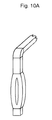
- a lead, 19 with a foot, 15 , extending parallel to the lead, as illustrated schematically in FIG. 10 , can be used thereby providing a surface mount lead for an electronic package.
- Another option is to provide a compliant pin lead for mechanical attachment as illustrated schematically in FIG. 10 a.
- FIGS. 11-13 An embodiment of the invention will be described with reference to FIGS. 11-13 wherein an electronic package, 103 , is schematically illustrated in partial cut-away end view, FIG. 11 , partial cut-away top view, FIG. 12 and partial cut-away side view, FIG. 13 .
- an electronic components, 1 of varying size are illustrated wherein each component comprises external terminations, 2 , on opposite sides wherein each external termination has at least one longitudinal edge and preferably multiple longitudinal edges.
- a laterally offset lead frame, 22 has a lateral step thereby allowing electronic components to be placed thereon wherein electronic components in a horizontal stack are of different lengths.
- Laterally offset as defined herein, is defined as offset in a plane parallel to the substrate upon which the electronic package is mounted.
- the laterally offset lead frame is illustrated with an optional stand-off feature, 21 , with the understanding that a foot, as illustrated in FIG. 10 , could be employed.
- an interconnect material, 3 preferably selected from TLPS, conductive epoxy, or polymer solder, along the longitudinal edges of the external terminations, 2 .
- the laterally offset lead frame allows for an array of electronic components of different sizes with the same electronic package.
- the entire electronic package, except for the stand-off feature and terminal end of the lead, are preferably encapsulated, 6 .
- An embodiment is illustrated in FIG.
- the short longitudinal side of the electronic components are mounted to the lead frame, 63 , and the lead frame has a foot, 64 .
- the electronic component can be mounted with either the longer longitudinal side or the shorter longitudinal side in electrical contact with the lead frame, or combinations thereof.
- additional rows and columns can be added with adjacent longitudinal edges of the external terminations bonded by an interconnect material which are not specifically illustrated for clarity.
- FIG. 14 is a partial cut-away side schematic view of an electronic package, generally represented at 104
- FIG. 15 is a partial cut-away edge schematic view.
- a horizontally offset lead frame, 24 is utilized to accommodate electronic components of different sizes. Isolated horizontally offset lead frames are illustrated in schematic side view in FIG. 16 .
- Horizontally offset as defined herein, is an offset in a plane perpendicular to the substrate upon which the electronic package is mounted.
- FIG. 17 An embodiment of the invention is illustrated in schematic cut-away side view in FIG. 17 wherein a flat lead frame, 4 , as described relative to FIG. 1 , is incorporated with secondary flat lead frames, 41 , wherein a secondary flat lead frame is in electrical contact with less than all of the electronic components of an electronic package.
- Lead frame, 4 for example could be ground with each lead frame 41 having a different functionality. It would be understood that additional capability can be incorporated with additional components being placed in electrical contact with lead 4 and a select lead 41 either directly or through the longitudinal edge of an adjacent component.
- An advantage of the invention is the fact that each stack, extending vertically away from the substrate is not limited in height by any other stack.
- Another option is to mount the components to the leads through the shorter of the longitudinal terminations as illustrated in FIG. 18 .
- the components, 2 are bonded to the flat surface of the lead frame 63 .
- the lead surface for bonding is thus minimized.
- the electronic package generally represented by 105 , comprises a first component, 86 , with a horizontally offset lead frame in electrical contact with each external termination, 286 and 287 .
- One horizontally offset lead frame, 81 is also in electrical contact with an external termination 289 of a second component, 87 .
- Another horizontally offset lead frame is in electrical contact with external termination 286 of component 86 and external termination 291 of component 88 .
- Horizontally offset lead frame 82 is in electrical contact with external termination 290 of component 87 and external termination of component 88 .
- the degree of offset can be varied depending on the components employed and the combinations of components, 290 , available is therefore very large in number.
- component 86 is an MLCC
- component 87 is a diode
- element 88 is a resistor
- an electronic package can be prepared with an electrical schematic diagram 89 as illustrated in FIG. 20 .
- a method of assembly could be easily implemented with the use of standard equipment and processes such as a lead frame carrier and/or pallet fixture for the part presentation and commercially available machines that are capable of applying interconnect materials, placing components, performing inspection, curing/reflowing/sintering interconnect materials, trimming/forming leads, and encapsulating the assembly.
- a through-hole assembly stand-off feature as utilized herein, provides a physical barrier to the insertion of a through hole beyond a certain depth.
- Transient liquid phase sintering adhesives are conductive materials that are distinguished from solders. Solders are alloys which do not undergo a change in composition after the first reflow. TLPS materials are mixtures of two or more metals or metal alloys prior to exposure to elevated temperatures. The second distinguishing characteristic of TLPS materials is that the melting point of the material is dependent on the thermal history of the material. TLPS materials exhibit a low melting point prior to exposure to elevated temperatures, and a higher melting point following exposure to these temperatures. The initial melting point is the result of the low temperature metal or an alloy of two low temperature metals.
- the second melting temperature is that of the intermetallic formed when the low temperature metal or alloy, forms a new alloy with a high temperature melting point metal thereby creating an intermetallic having a higher melting point.
- TLPS materials form a metallurgical bond between the metal surfaces to be joined. Unlike tin/lead or lead (Pb) free solders, the TLPS conductive adhesives do not spread as they form the intermetallic joint. Rework of the TLPS system is very difficult due to the high secondary reflow temperatures.
- Conductive adhesives comprise conductive metal, typically silver, filled polymers that cure or cross link within a specified temperature range, generally 150° C., to form a mechanical bond to the materials to be joined. Their conductivity is created by the metal particles which make intimate contact with one another, within the confines of the polymer matrix, to form an electrically conductive path from one particle to another. Because the binder is organic in nature, they have relatively low temperature capabilities, normally in the range of about 150° C. to about 300° C. Conductive epoxies, once cured, cannot be reworked. Conductive epoxies do not wet or flow as they cure as do solders when they melt.
- Polymer solders may comprise conventional solder systems based on Pb/Sn alloy systems or lead free systems, such as Sn/Sb, which are combined with cross linking polymers which serve as cleaning agents.
- the cross-linked polymers also have the ability to form a cross-linked polymer bond, such as an epoxy bond, that forms during the melting phase of the metals thereby forming a solder alloy and a mechanical polymeric bond.
- An advantage of polymer solders is that the polymeric bond provides additional mechanical bond strength at temperatures above the melting point of the solder, thus giving the solder joint a higher operating temperature in the range of about 5 to 80° C. above the melting point of the solder.
- Polymer solders combine current solder alloys with a cross linking polymer within the same paste to provide both a metallurgical bond and a mechanical bond when cured, such as by heating, to provide additional solder joint strength at elevated temperatures.
- the upper temperature limits and joint strength has been increased, just by the physical properties of the materials. A practical limit of 300° C. remains whereas the transient liquid phase sintering conductive adhesives can achieve higher temperatures.
- conductive adhesives and conductive polymers can be coated onto one side being bonded.
- the conductive adhesive can be placed on either the lead or the longitudinal edge.
- the component and lead can be placed into position with the interconnect thereby between followed by heating to form the bond there between.
- TLPS comprise high temperature materials selected from copper, silver, aluminum, gold, platinum, palladium, beryllium, rhodium, nickel, cobalt, iron and molybdenum or a mixture or any combination thereof are suitable for use in transient liquid phase sintering conductive adhesives.
- the lead (Pb) free transient liquid phase sintering adhesives preferably use either silver or copper as the high temperature component and a tin-bismuth alloy as the low temperature component.
- TLPS further comprises low temperature materials selected from tin, antimony, bismuth, cadmium, zinc, gallium, indium, tellurium, mercury, thallium, selenium, or polonium, or a mixture or an alloy of any two or more of these.
- the transient liquid phase sintering conductive adhesives are compatible with surface finishes containing silver, tin, gold, copper, platinum, palladium, nickel, or combinations thereof, either as lead frame finishes, component connections or inner electrodes to form an electronically conductive metallurgical bond between two surfaces.
- Suitable external lead or lead frame materials include phosphor bronze, copper, alloys of copper such as but not limited to beryllium copper, Cu194 and Cu192, as well as lead frames consisting of ferrous alloys such as but not limited to Alloy 42 and Kovar.
- a particular advantage of the TLPS is the flexibility provided in assembly.
- the high temperature component and low temperature component can be coated on one of the layers being bonded.
- the elements of the TLPS can be coated on either the lead or the longitudinal edge and heated to form the bond after the component and lead are brought into relationship with the TLPS components there between.
- one component of the TLPS can be coated on the lead and the other coated on the longitudinal edge with heating after the component and lead are brought into relationship to form the bond.
- one component of the TLPS can be coated on one side being bonded, the lead for example, and the other component of the TLPS can be coated on the other side being bonded, an external termination for example. The components can be brought into contact followed by heating to form the TLPS bond.
Landscapes
- Engineering & Computer Science (AREA)
- Power Engineering (AREA)
- Microelectronics & Electronic Packaging (AREA)
- Manufacturing & Machinery (AREA)
- Lead Frames For Integrated Circuits (AREA)
Abstract
Description
- providing a multiplicity of electronic components wherein each electronic component comprises a first external termination with at least one first longitudinal edge and a second external termination with at least on second longitudinal edge;
- placing a first lead into contact with the first longitudinal edge with a first interconnect between the first lead and the first longitudinal edge;
- placing a second lead into contact with the second longitudinal edge with a second interconnect between the second lead and the second longitudinal edge; and
- heating to form a bond of the first interconnect and the second interconnect.
Claims (38)
Priority Applications (9)
| Application Number | Priority Date | Filing Date | Title |
|---|---|---|---|
| US14/963,766 US9805872B2 (en) | 2015-12-09 | 2015-12-09 | Multiple MLCC modules |
| US15/264,305 US10224149B2 (en) | 2015-12-09 | 2016-09-13 | Bulk MLCC capacitor module |
| JP2018529086A JP7250517B2 (en) | 2015-12-09 | 2016-12-01 | Bulk MLCC capacitor module |
| CN201680072483.3A CN108369864A (en) | 2015-12-09 | 2016-12-01 | Large capacity MLCC capacitor module |
| PCT/US2016/064401 WO2017100073A1 (en) | 2015-12-09 | 2016-12-01 | Bulk mlcc capacitor module |
| EP16873625.4A EP3387659A4 (en) | 2015-12-09 | 2016-12-01 | CONDENSER MODULE MLCC BULK PRODUCT |
| US15/670,247 US10381162B2 (en) | 2010-05-26 | 2017-08-07 | Leadless stack comprising multiple components |
| US16/456,912 US10790094B2 (en) | 2010-05-26 | 2019-06-28 | Method of forming a leadless stack comprising multiple components |
| JP2022087842A JP2022119920A (en) | 2015-12-09 | 2022-05-30 | Bulk MLCC capacitor module |
Applications Claiming Priority (1)
| Application Number | Priority Date | Filing Date | Title |
|---|---|---|---|
| US14/963,766 US9805872B2 (en) | 2015-12-09 | 2015-12-09 | Multiple MLCC modules |
Related Child Applications (4)
| Application Number | Title | Priority Date | Filing Date |
|---|---|---|---|
| US13/114,126 Continuation-In-Part US8902565B2 (en) | 2010-05-26 | 2011-05-24 | Electronic component termination and assembly by means of transient liquid phase sintering and polymer solder pastes |
| US15/264,305 Continuation-In-Part US10224149B2 (en) | 2015-12-09 | 2016-09-13 | Bulk MLCC capacitor module |
| US15/285,210 Continuation-In-Part US10366836B2 (en) | 2010-05-26 | 2016-10-04 | Electronic component structures with reduced microphonic noise |
| US15/670,247 Continuation-In-Part US10381162B2 (en) | 2010-05-26 | 2017-08-07 | Leadless stack comprising multiple components |
Publications (2)
| Publication Number | Publication Date |
|---|---|
| US20170169955A1 US20170169955A1 (en) | 2017-06-15 |
| US9805872B2 true US9805872B2 (en) | 2017-10-31 |
Family
ID=59020159
Family Applications (1)
| Application Number | Title | Priority Date | Filing Date |
|---|---|---|---|
| US14/963,766 Active 2036-04-03 US9805872B2 (en) | 2010-05-26 | 2015-12-09 | Multiple MLCC modules |
Country Status (1)
| Country | Link |
|---|---|
| US (1) | US9805872B2 (en) |
Cited By (3)
| Publication number | Priority date | Publication date | Assignee | Title |
|---|---|---|---|---|
| US20170367228A1 (en) * | 2016-06-20 | 2017-12-21 | Kemet Electronics Corporation | Component Stability Structure |
| US11222752B2 (en) * | 2019-10-28 | 2022-01-11 | Tdk Corporation | Ceramic electronic device |
| US11581141B2 (en) * | 2020-03-02 | 2023-02-14 | Holy Stone Enierprise Co., Ltd. | Leadless stack comprising ceramic capacitor |
Families Citing this family (7)
| Publication number | Priority date | Publication date | Assignee | Title |
|---|---|---|---|---|
| US10366836B2 (en) | 2010-05-26 | 2019-07-30 | Kemet Electronics Corporation | Electronic component structures with reduced microphonic noise |
| US9472342B2 (en) | 2010-05-26 | 2016-10-18 | Kemet Electronics Corporation | Leadless multi-layered ceramic capacitor stacks |
| US10381162B2 (en) | 2010-05-26 | 2019-08-13 | Kemet Electronics Corporation | Leadless stack comprising multiple components |
| EP3306631B1 (en) * | 2016-10-04 | 2025-05-21 | Kemet Electronics Corporation | Electronic device |
| EP3522188A1 (en) * | 2018-02-06 | 2019-08-07 | Siemens Aktiengesellschaft | Capacitor structure and power module with a high performance electronics component |
| DE102018201842A1 (en) | 2018-02-06 | 2019-08-08 | Siemens Aktiengesellschaft | Power electronic circuit with multiple power modules |
| US10910163B2 (en) * | 2018-06-29 | 2021-02-02 | Samsung Electro-Mechanics Co., Ltd. | Multilayer electronic component and board having the same mounted thereon |
Citations (17)
| Publication number | Priority date | Publication date | Assignee | Title |
|---|---|---|---|---|
| US6721163B2 (en) | 2001-12-06 | 2004-04-13 | Denso Corporation | Stacked ceramic body and production method thereof |
| US6940708B2 (en) | 2003-08-19 | 2005-09-06 | Tdk Corporation | Electronic component |
| US6958899B2 (en) | 2003-03-20 | 2005-10-25 | Tdk Corporation | Electronic device |
| US20100243307A1 (en) | 2009-03-26 | 2010-09-30 | Mcconnell John E | Leaded multi-layer ceramic capacitor with low esl and low esr |
| US8264816B2 (en) | 2009-08-24 | 2012-09-11 | Kemet Electronics Corporation | Externally fused and resistively loaded safety capacitor |
| US20140160624A1 (en) | 2012-12-06 | 2014-06-12 | Kemet Electronics Corporation | Multi-Layered Ceramic Capacitor with Soft Leaded Module |
| US20140230941A1 (en) | 2011-10-14 | 2014-08-21 | Voss Automotive Gmbh | At least partially heatable line-connector for a heatable media line, and an assembled media line comprising such a line-connector |
| US20140238732A1 (en) | 2013-02-28 | 2014-08-28 | Murata Manufacturing Co., Ltd. | Electronic part and electronic control unit |
| US20140240885A1 (en) | 2013-02-28 | 2014-08-28 | Murata Manufacturing Co., Ltd. | Electronic part and electronic control unit |
| US20140240081A1 (en) | 2013-02-28 | 2014-08-28 | Murata Manufacturing Co., Ltd. | Electronic part and electronic control unit |
| US20140240942A1 (en) | 2013-02-28 | 2014-08-28 | Murata Manufacturing Co., Ltd. | Electronic part and electronic control unit |
| US20140240941A1 (en) * | 2013-02-28 | 2014-08-28 | Murata Manufacturing Co., Ltd. | Electronic part and electronic control unit |
| US8873219B2 (en) | 2012-06-26 | 2014-10-28 | Kemet Electronics Corporation | Method for stacking electronic components |
| US20140345926A1 (en) | 2013-05-21 | 2014-11-27 | Samsung Electro-Mechanics Co., Ltd. | Multilayered ceramic capacitor and board for mounting the same |
| US8988857B2 (en) | 2011-12-13 | 2015-03-24 | Kemet Electronics Corporation | High aspect ratio stacked MLCC design |
| US20150187502A1 (en) * | 2013-12-31 | 2015-07-02 | Hyundai Mobis Co., Ltd. | Capacitor module, method for manufacturing the same, and inverter for vehicle having the same |
| US20150310991A1 (en) | 2014-04-29 | 2015-10-29 | Apple Inc. | Multi-layered ceramic capacitors |
-
2015
- 2015-12-09 US US14/963,766 patent/US9805872B2/en active Active
Patent Citations (18)
| Publication number | Priority date | Publication date | Assignee | Title |
|---|---|---|---|---|
| US6721163B2 (en) | 2001-12-06 | 2004-04-13 | Denso Corporation | Stacked ceramic body and production method thereof |
| US6958899B2 (en) | 2003-03-20 | 2005-10-25 | Tdk Corporation | Electronic device |
| US6940708B2 (en) | 2003-08-19 | 2005-09-06 | Tdk Corporation | Electronic component |
| US20100243307A1 (en) | 2009-03-26 | 2010-09-30 | Mcconnell John E | Leaded multi-layer ceramic capacitor with low esl and low esr |
| US8264816B2 (en) | 2009-08-24 | 2012-09-11 | Kemet Electronics Corporation | Externally fused and resistively loaded safety capacitor |
| US8904609B2 (en) | 2009-08-24 | 2014-12-09 | Kemet Electronics Corporation | Externally fused and resistively loaded safety capacitor |
| US20140230941A1 (en) | 2011-10-14 | 2014-08-21 | Voss Automotive Gmbh | At least partially heatable line-connector for a heatable media line, and an assembled media line comprising such a line-connector |
| US8988857B2 (en) | 2011-12-13 | 2015-03-24 | Kemet Electronics Corporation | High aspect ratio stacked MLCC design |
| US8873219B2 (en) | 2012-06-26 | 2014-10-28 | Kemet Electronics Corporation | Method for stacking electronic components |
| US20140160624A1 (en) | 2012-12-06 | 2014-06-12 | Kemet Electronics Corporation | Multi-Layered Ceramic Capacitor with Soft Leaded Module |
| US20140240081A1 (en) | 2013-02-28 | 2014-08-28 | Murata Manufacturing Co., Ltd. | Electronic part and electronic control unit |
| US20140240942A1 (en) | 2013-02-28 | 2014-08-28 | Murata Manufacturing Co., Ltd. | Electronic part and electronic control unit |
| US20140240941A1 (en) * | 2013-02-28 | 2014-08-28 | Murata Manufacturing Co., Ltd. | Electronic part and electronic control unit |
| US20140240885A1 (en) | 2013-02-28 | 2014-08-28 | Murata Manufacturing Co., Ltd. | Electronic part and electronic control unit |
| US20140238732A1 (en) | 2013-02-28 | 2014-08-28 | Murata Manufacturing Co., Ltd. | Electronic part and electronic control unit |
| US20140345926A1 (en) | 2013-05-21 | 2014-11-27 | Samsung Electro-Mechanics Co., Ltd. | Multilayered ceramic capacitor and board for mounting the same |
| US20150187502A1 (en) * | 2013-12-31 | 2015-07-02 | Hyundai Mobis Co., Ltd. | Capacitor module, method for manufacturing the same, and inverter for vehicle having the same |
| US20150310991A1 (en) | 2014-04-29 | 2015-10-29 | Apple Inc. | Multi-layered ceramic capacitors |
Non-Patent Citations (1)
| Title |
|---|
| ISA/US: International Search Report and Written Opinion issued in PCT/US2016/064401 for Kemet Electronics Corporation; dated Apr. 14, 2017. |
Cited By (5)
| Publication number | Priority date | Publication date | Assignee | Title |
|---|---|---|---|---|
| US20170367228A1 (en) * | 2016-06-20 | 2017-12-21 | Kemet Electronics Corporation | Component Stability Structure |
| US10729051B2 (en) * | 2016-06-20 | 2020-07-28 | Kemet Electronics Corporation | Component stability structure |
| US11432448B2 (en) * | 2016-06-20 | 2022-08-30 | Kemet Electronics Corporation | Method of forming an electronic device |
| US11222752B2 (en) * | 2019-10-28 | 2022-01-11 | Tdk Corporation | Ceramic electronic device |
| US11581141B2 (en) * | 2020-03-02 | 2023-02-14 | Holy Stone Enierprise Co., Ltd. | Leadless stack comprising ceramic capacitor |
Also Published As
| Publication number | Publication date |
|---|---|
| US20170169955A1 (en) | 2017-06-15 |
Similar Documents
| Publication | Publication Date | Title |
|---|---|---|
| US10224149B2 (en) | Bulk MLCC capacitor module | |
| US9805872B2 (en) | Multiple MLCC modules | |
| US10707145B2 (en) | High density multi-component packages | |
| US5729438A (en) | Discrete component pad array carrier | |
| US10757810B2 (en) | High density multi-component packages | |
| US20050011672A1 (en) | Overmolded MCM with increased surface mount component reliability | |
| KR960016651A (en) | Electrically Conductive Paste Materials and Applications | |
| US20100246149A1 (en) | Connection member and printed circuit board unit | |
| US10757811B2 (en) | Higher density multi-component and serial packages | |
| EP0027017B1 (en) | Integrated circuit package | |
| CN104637914B (en) | Multifunctional surface-mount electronic component and method for manufacturing the same | |
| US10707403B2 (en) | Electronic component-containing module | |
| EP3679599A1 (en) | High density multi-component and serial packages | |
| CN1953174B (en) | Module with embedded electronic components | |
| US11923151B2 (en) | Structural lead frame | |
| US6618269B2 (en) | Discrete circuit component and process of fabrication | |
| CN219476684U (en) | SMD LED containing control element | |
| US9640475B1 (en) | Chip packaging structure and manufacturing method thereof | |
| JP2005159227A (en) | Circuit component built-in module and manufacturing method thereof | |
| US10121753B2 (en) | Enhanced solder pad | |
| JP2002076193A (en) | Package for mounting semiconductor element and package mounting board |
Legal Events
| Date | Code | Title | Description |
|---|---|---|---|
| AS | Assignment |
Owner name: KEMET ELECTRONICS CORPORATION, SOUTH CAROLINA Free format text: ASSIGNMENT OF ASSIGNORS INTEREST;ASSIGNORS:MILLER, GALEN W.;MCCONNELL, JOHN E.;BULTITUDE, JOHN;AND OTHERS;REEL/FRAME:037249/0324 Effective date: 20151116 |
|
| AS | Assignment |
Owner name: BANK OF AMERICA, N.A., AS COLLATERAL AGENT, NORTH Free format text: SECURITY AGREEMENT;ASSIGNORS:KEMET CORPORATION;KEMET ELECTRONICS CORPORATION;KEMET BLUE POWDER CORPORATION;REEL/FRAME:042523/0639 Effective date: 20170505 Owner name: BANK OF AMERICA, N.A., AS COLLATERAL AGENT, NORTH CAROLINA Free format text: SECURITY AGREEMENT;ASSIGNORS:KEMET CORPORATION;KEMET ELECTRONICS CORPORATION;KEMET BLUE POWDER CORPORATION;REEL/FRAME:042523/0639 Effective date: 20170505 |
|
| STCF | Information on status: patent grant |
Free format text: PATENTED CASE |
|
| AS | Assignment |
Owner name: KEMET BLUE POWDER CORPORATION, NEVADA Free format text: RELEASE BY SECURED PARTY;ASSIGNOR:BANK OF AMERICA, N.A.;REEL/FRAME:047450/0926 Effective date: 20181107 Owner name: KEMET ELECTRONICS CORPORATION, FLORIDA Free format text: RELEASE BY SECURED PARTY;ASSIGNOR:BANK OF AMERICA, N.A.;REEL/FRAME:047450/0926 Effective date: 20181107 Owner name: KEMET CORPORATION,, FLORIDA Free format text: RELEASE BY SECURED PARTY;ASSIGNOR:BANK OF AMERICA, N.A.;REEL/FRAME:047450/0926 Effective date: 20181107 |
|
| MAFP | Maintenance fee payment |
Free format text: PAYMENT OF MAINTENANCE FEE, 4TH YEAR, LARGE ENTITY (ORIGINAL EVENT CODE: M1551); ENTITY STATUS OF PATENT OWNER: LARGE ENTITY Year of fee payment: 4 |
|
| MAFP | Maintenance fee payment |
Free format text: PAYMENT OF MAINTENANCE FEE, 8TH YEAR, LARGE ENTITY (ORIGINAL EVENT CODE: M1552); ENTITY STATUS OF PATENT OWNER: LARGE ENTITY Year of fee payment: 8 |