US9805651B2 - Organic light emitting display apparatus - Google Patents
Organic light emitting display apparatus Download PDFInfo
- Publication number
- US9805651B2 US9805651B2 US14/657,219 US201514657219A US9805651B2 US 9805651 B2 US9805651 B2 US 9805651B2 US 201514657219 A US201514657219 A US 201514657219A US 9805651 B2 US9805651 B2 US 9805651B2
- Authority
- US
- United States
- Prior art keywords
- light
- transistor
- control signal
- driving
- electrode
- Prior art date
- Legal status (The legal status is an assumption and is not a legal conclusion. Google has not performed a legal analysis and makes no representation as to the accuracy of the status listed.)
- Active, expires
Links
Images


Classifications
-
- G—PHYSICS
- G09—EDUCATION; CRYPTOGRAPHY; DISPLAY; ADVERTISING; SEALS
- G09G—ARRANGEMENTS OR CIRCUITS FOR CONTROL OF INDICATING DEVICES USING STATIC MEANS TO PRESENT VARIABLE INFORMATION
- G09G3/00—Control arrangements or circuits, of interest only in connection with visual indicators other than cathode-ray tubes
- G09G3/20—Control arrangements or circuits, of interest only in connection with visual indicators other than cathode-ray tubes for presentation of an assembly of a number of characters, e.g. a page, by composing the assembly by combination of individual elements arranged in a matrix no fixed position being assigned to or needed to be assigned to the individual characters or partial characters
- G09G3/22—Control arrangements or circuits, of interest only in connection with visual indicators other than cathode-ray tubes for presentation of an assembly of a number of characters, e.g. a page, by composing the assembly by combination of individual elements arranged in a matrix no fixed position being assigned to or needed to be assigned to the individual characters or partial characters using controlled light sources
- G09G3/30—Control arrangements or circuits, of interest only in connection with visual indicators other than cathode-ray tubes for presentation of an assembly of a number of characters, e.g. a page, by composing the assembly by combination of individual elements arranged in a matrix no fixed position being assigned to or needed to be assigned to the individual characters or partial characters using controlled light sources using electroluminescent panels
- G09G3/32—Control arrangements or circuits, of interest only in connection with visual indicators other than cathode-ray tubes for presentation of an assembly of a number of characters, e.g. a page, by composing the assembly by combination of individual elements arranged in a matrix no fixed position being assigned to or needed to be assigned to the individual characters or partial characters using controlled light sources using electroluminescent panels semiconductive, e.g. using light-emitting diodes [LED]
- G09G3/3208—Control arrangements or circuits, of interest only in connection with visual indicators other than cathode-ray tubes for presentation of an assembly of a number of characters, e.g. a page, by composing the assembly by combination of individual elements arranged in a matrix no fixed position being assigned to or needed to be assigned to the individual characters or partial characters using controlled light sources using electroluminescent panels semiconductive, e.g. using light-emitting diodes [LED] organic, e.g. using organic light-emitting diodes [OLED]
- G09G3/3225—Control arrangements or circuits, of interest only in connection with visual indicators other than cathode-ray tubes for presentation of an assembly of a number of characters, e.g. a page, by composing the assembly by combination of individual elements arranged in a matrix no fixed position being assigned to or needed to be assigned to the individual characters or partial characters using controlled light sources using electroluminescent panels semiconductive, e.g. using light-emitting diodes [LED] organic, e.g. using organic light-emitting diodes [OLED] using an active matrix
- G09G3/3233—Control arrangements or circuits, of interest only in connection with visual indicators other than cathode-ray tubes for presentation of an assembly of a number of characters, e.g. a page, by composing the assembly by combination of individual elements arranged in a matrix no fixed position being assigned to or needed to be assigned to the individual characters or partial characters using controlled light sources using electroluminescent panels semiconductive, e.g. using light-emitting diodes [LED] organic, e.g. using organic light-emitting diodes [OLED] using an active matrix with pixel circuitry controlling the current through the light-emitting element
-
- G—PHYSICS
- G09—EDUCATION; CRYPTOGRAPHY; DISPLAY; ADVERTISING; SEALS
- G09G—ARRANGEMENTS OR CIRCUITS FOR CONTROL OF INDICATING DEVICES USING STATIC MEANS TO PRESENT VARIABLE INFORMATION
- G09G5/00—Control arrangements or circuits for visual indicators common to cathode-ray tube indicators and other visual indicators
- G09G5/02—Control arrangements or circuits for visual indicators common to cathode-ray tube indicators and other visual indicators characterised by the way in which colour is displayed
-
- G—PHYSICS
- G09—EDUCATION; CRYPTOGRAPHY; DISPLAY; ADVERTISING; SEALS
- G09G—ARRANGEMENTS OR CIRCUITS FOR CONTROL OF INDICATING DEVICES USING STATIC MEANS TO PRESENT VARIABLE INFORMATION
- G09G2300/00—Aspects of the constitution of display devices
- G09G2300/08—Active matrix structure, i.e. with use of active elements, inclusive of non-linear two terminal elements, in the pixels together with light emitting or modulating elements
- G09G2300/0809—Several active elements per pixel in active matrix panels
- G09G2300/0842—Several active elements per pixel in active matrix panels forming a memory circuit, e.g. a dynamic memory with one capacitor
- G09G2300/0861—Several active elements per pixel in active matrix panels forming a memory circuit, e.g. a dynamic memory with one capacitor with additional control of the display period without amending the charge stored in a pixel memory, e.g. by means of additional select electrodes
- G09G2300/0866—Several active elements per pixel in active matrix panels forming a memory circuit, e.g. a dynamic memory with one capacitor with additional control of the display period without amending the charge stored in a pixel memory, e.g. by means of additional select electrodes by means of changes in the pixel supply voltage
-
- G—PHYSICS
- G09—EDUCATION; CRYPTOGRAPHY; DISPLAY; ADVERTISING; SEALS
- G09G—ARRANGEMENTS OR CIRCUITS FOR CONTROL OF INDICATING DEVICES USING STATIC MEANS TO PRESENT VARIABLE INFORMATION
- G09G2310/00—Command of the display device
- G09G2310/02—Addressing, scanning or driving the display screen or processing steps related thereto
- G09G2310/0243—Details of the generation of driving signals
- G09G2310/0251—Precharge or discharge of pixel before applying new pixel voltage
-
- G—PHYSICS
- G09—EDUCATION; CRYPTOGRAPHY; DISPLAY; ADVERTISING; SEALS
- G09G—ARRANGEMENTS OR CIRCUITS FOR CONTROL OF INDICATING DEVICES USING STATIC MEANS TO PRESENT VARIABLE INFORMATION
- G09G2310/00—Command of the display device
- G09G2310/02—Addressing, scanning or driving the display screen or processing steps related thereto
- G09G2310/0262—The addressing of the pixel, in a display other than an active matrix LCD, involving the control of two or more scan electrodes or two or more data electrodes, e.g. pixel voltage dependent on signals of two data electrodes
-
- G—PHYSICS
- G09—EDUCATION; CRYPTOGRAPHY; DISPLAY; ADVERTISING; SEALS
- G09G—ARRANGEMENTS OR CIRCUITS FOR CONTROL OF INDICATING DEVICES USING STATIC MEANS TO PRESENT VARIABLE INFORMATION
- G09G2320/00—Control of display operating conditions
- G09G2320/02—Improving the quality of display appearance
- G09G2320/0242—Compensation of deficiencies in the appearance of colours
Definitions
- One or more embodiments described herein relate to an organic light emitting display apparatus.
- An organic light emitting display uses sub-pixels to emit light of different colors. Each sub-pixel is driven by a current which flows based on an applied voltage The level of the voltage required for each sub-pixel may differ based on the color of light to be emitted. As a result, the time required for the sub-pixel to emit one color of light may be different from a sub-pixel that emits another color of light. This difference may cause the combined light from a unit pixel to be different from a desired color.
- an organic light-emitting display apparatus includes a pixel circuit to output a driving current to a node based on a data signal; a light emitter to emit light based on the driving current at the node; a transistor to output an initial voltage to the node based on a first control signal received through a first control line; and a coupling capacitor between the node and the first control line.
- the transistor may initialize a potential of the node, and the potential may change in synchronization with an edge of the first control signal by the coupling capacitor.
- the apparatus includes a first sub-pixel to emit light of a first color, the first sub-pixel including the pixel circuit, the light-emitter, the transistor, and the coupling capacitor; and a second sub-pixel to emit light of a second color different from the first color, the second sub-pixel including a pixel circuit, a light-emitter, and an initialization transistor.
- the light-emitter of the first sub-pixel may have a threshold voltage different from the light-emitter of the second sub-pixel.
- the apparatus may include a plurality of lines connected to the pixel circuit, wherein the plurality of lines may include a driving voltage line to carry a first driving voltage, a data line to carry the data signal, a second control line to carry a second control signal, a third control line to carry a third control signal, and a fourth control line to carry a fourth control signal, and wherein the second control signal, the third control signal, and the first control signal may have active periods in an inactive period of the fourth control signal.
- the pixel circuit may include a driving transistor having a first electrode to receive the first driving voltage and a second electrode connected to the node; and a switching transistor having a first electrode to receive a data signal and a second electrode connected to the first electrode of the driving transistor, wherein the driving transistor may supply the driving current corresponding to the data signal to the light-emitter according to a switching operation of the switching transistor.
- the pixel circuit may include a gate initialization transistor to supply the initial voltage to a gate electrode of the driving transistor based on the second control signal; a compensation transistor to connect the gate electrode of the driving transistor to the second electrode of the driving transistor based on the third control signal; a first light-emitting control transistor to output the driving current to the node based on the fourth control signal; and a storage capacitor to store a voltage difference between the first driving voltage and a voltage of the gate electrode of the driving transistor.
- the gate initialization transistor may include a gate electrode connected to the second control line, a first electrode to receive the initial voltage, and a second electrode connected to the gate electrode of the driving transistor
- the compensation transistor may include a gate electrode connected to the third control line, a first electrode connected to the gate electrode of the driving transistor, and a second electrode connected to the second electrode of the driving transistor
- a second light-emitting control transistor may connect the driving transistor and the driving voltage line, wherein the first light-emitting transistor is to connect the driving transistor to the light-emitter.
- an organic light-emitting display apparatus includes a plurality of first sub-pixels, a plurality of second sub-pixels, and a plurality of third sub-pixels, wherein each of the first through third sub-pixels includes: a pixel circuit to output a driving current to a node based on a data signal; a light-emitter to emit light based on the driving current at the node; and a transistor to output an initial voltage to the node based on a first control signal carried through a first control line, wherein at least one of the first through third sub-pixels includes a coupling capacitor between the node and the first control line.
- a potential of the node may be initialized based on the initial voltage from the transistor, the potential changing in synchronization with an edge of the first control signal by the coupling capacitor.
- the apparatus may include a plurality of lines connected to the pixel circuit, wherein the plurality of lines may include a driving voltage line to carry a first driving voltage, a data line to carry the data signal, a second control line to carry a second control signal, a third control line to carry a third control signal, and a fourth control line to carry a fourth control signal, and wherein the second control signal, the third control signal, and the first control signal may have active periods in an inactive period of the fourth control signal.
- the pixel circuit may include a driving transistor having a first electrode to receive the first driving voltage and a second electrode connected to the node; a switching transistor having a first electrode to receive a data signal and a second electrode connected to the first electrode of the driving transistor; a gate initialization transistor to supply the initial voltage to a gate electrode of the driving transistor based on the second control signal; a compensation transistor to connect the gate electrode of the driving transistor to the second electrode of the driving transistor based on the third control signal; a light-emitting control transistor to output the driving current to the node based on the fourth control signal; and a storage capacitor to store a voltage difference between the first driving voltage and a voltage of the gate electrode of the driving transistor.
- the driving transistor may supply a driving current corresponding to the data signal to the light-emitter according to a switching operation of the switching transistor.
- the coupling capacitor may be coupled to the light-emitter, and the light emitter may emit green light
- an organic light-emitting display apparatus a pixel circuit to output a driving current to a node based on a data signal; a light-emitter to emit
- a transistor to output an initial voltage to the node based on a first control signal through a first control line, wherein: a coupling capacitance is between the node and the first control line, and a potential of the node changes in synchronization with an edge of the first control signal.
- the apparatus may include a coupling capacitor between the node and the first control line, the coupling capacitor having the coupling capacitance.
- the apparatus may include a first sub-pixel to emit light of a first color, the first sub-pixel including the pixel circuit, the light-emitter, the transistor, and the coupling capacitor; and a second sub-pixel to emit light of a second color different from the first color, the second sub-pixel including a pixel circuit, a light-emitter, and an initialization transistor.
- the light-emitter of the first sub-pixel may have a threshold voltage different from the light-emitting device of the second sub-pixel.
- the coupling capacitance of the coupling capacitor of the first sub-pixel may be different from a coupling capacitance between a node coupled to the second sub-pixel and a control line.
- the apparatus may include a plurality of lines connected to the pixel circuit, wherein the plurality of lines include a driving voltage line to carry a first driving voltage, a data line to carry the data signal, a second control line to carry a second control signal, a third control line to carry a third control signal, and a fourth control line to carry a fourth control signal, and wherein the second control signal, the third control signal, and the first control signal have active periods in an inactive period of the fourth control signal.
- the pixel circuit may include a driving transistor having a first electrode to receive the first driving voltage and a second electrode connected to the output node; a switching transistor including a first electrode to receive a data signal and a second electrode connected to the first electrode of the driving transistor; a gate initialization transistor to supply the initial voltage to a gate electrode of the driving transistor in response to the second control signal; a compensation transistor to connect the gate electrode of the driving transistor to the second electrode of the driving transistor based on the third control signal; a light-emitting control transistor to output the driving current to the node based on the fourth control signal; and a storage capacitor to store a voltage difference between the first driving voltage and a voltage of the gate electrode of the driving transistor, wherein the driving transistor is to supply a driving current corresponding to the data signal to the light-emitter based on a switching operation of the switching transistor.
- FIG. 1 illustrates an embodiment of an organic light emitting display
- FIG. 2 illustrates an example of a difference in a light-emitting time points between sub-pixels
- FIGS. 3 and 4 illustrate examples of sub-pixels
- FIG. 5 illustrates an example of control signals for a first sub-pixel
- FIG. 6 illustrates an example of control signals for a second sub-pixel
- FIG. 7 illustrates another example of control signals for a second sub-pixel
- FIG. 8 illustrates another embodiment of a display panel
- FIG. 9 illustrates another example of a first sub-pixel
- FIG. 10 illustrates another example of a second sub-pixel.
- FIG. 1 illustrates an embodiment of an organic light-emitting display which includes a plurality of pixels PX, each of which includes a first sub-pixel SP 1 , a second sub-pixel SP 2 , and a third sub-pixel SP 3 .
- Each sub-pixel SP 1 , SP 2 , and SP 3 includes a light-emitting device to emit light of a predetermined color, e.g., one selected from red R, green G, or blue B.
- the sub-pixels SP 1 , SP 2 , and SP 3 emit red R, green G, and blue B light, respectively.
- the organic light-emitting display apparatus may optionally include another sub-pixel having a light-emitting device to emit light of another color, e.g., white or yellow.
- FIG. 2 is a graph illustrating an example of a difference in a light-emitting time points between sub-pixels which emit different colors of light.
- the vertical axis corresponds to the amount of driving current for the sub-pixels.
- the horizontal axis correspond to time.
- first and second sub-pixels may have a same structure. Curve I shows the current flowing through the light-emitting device of the first sub-pixel, and Curve II shows the current flowing through the light-emitting device of the second sub-pixel.
- the first sub-pixel starts to emit light at a time point I corresponding to Curve I
- the second sub-pixel starts to emit light at a time point II corresponding to Curve II.
- Such a phenomenon may not occur in sub-pixels which emit light of the same color.
- the light-emitting time points are different in the case of FIG. 2 for sub-pixels that emit light of different colors.
- the first light-emitting device of the first sub-pixel includes a first light-emitting material emitting light of a first color.
- the second light-emitting device of the second sub-pixel includes a second light-emitting material emitting light of a second color.
- the first and second light-emitting materials have different characteristics, e.g., different size threshold voltages, different light-emitting efficiencies, etc.
- the level of the threshold voltage of the first light-emitting device may be different from that of a threshold voltage of the second light-emitting device.
- the light-emitting efficiency of the first light-emitting device may be different from the second light-emitting device.
- the first light-emitting device and the second light-emitting device may have different capacitances according to sizes and manufacturing processes of the first and second light-emitting devices.
- the light-emitting time point of the first light-emitting device may precede that of the second light-emitting device.
- the sizes of driving currents of the light-emitting devices may also be different. That is, when a light-emitting efficiency is relatively high, the size of a driving current may be lowered because the same amount of light may be generated by a relatively small amount of current. For example, the light-emitting efficiency of the first light-emitting device may be lower than the second light-emitting device. In this case, the size of the driving current of the first light-emitting device may be larger than the driving current of the second light-emitting device.
- the time required for the second light-emitting device to charge up to a threshold voltage by the driving voltage may be relatively long compared to the first light-emitting device.
- Curve II may correspond to a sub-pixel which includes a light-emitting material having a relatively high threshold voltage, or a sub-pixel including a light-emitting material having a relatively high light-emitting efficiency.
- Curve I may correspond to a sub-pixel including a light-emitting material having a relatively low threshold voltage, or a sub-pixel including a light-emitting material having a relatively low light-emitting efficiency.
- the light-emitting time point of a sub-pixel e.g., the first sub-pixel
- a light-emitting time point of a sub-pixel e.g., the second sub-pixel
- the light of the other color may be insufficient.
- a color spreading phenomenon may occur.
- FIGS. 3 and 4 are examples of circuit diagrams of a sub-pixel of the organic light-emitting display apparatus in FIG. 1 .
- FIGS. 3 and 4 may be circuit diagrams of any one of the sub-pixels in FIG. 1 .
- a sub-pixel corresponding to the circuit diagram of FIG. 3 is referred to as a first sub-pixel SPa, and a sub-pixel corresponding to the circuit diagram of FIG. 4 is referred to as a second sub-pixel SPb.
- Each of the first and second sub-pixels SPa and SPb includes a pixel circuit P that receives a data signal and outputs a driving current corresponding to the received data signal.
- the driving current is output to an output node Node_out, coupled to a light-emitting device OLED that emits light based on the driving current input to the output node Node_out.
- An anode initialization transistor T 7 outputs an initial voltage Vinit to the output node Node_out in response to a first control signal received through a first control line CL 1 .
- the pixel circuit P includes a plurality of lines which include, for example, a driving voltage line ELVDDL carrying a first driving voltage, a data line DL carrying the data signal, a second control line CL 2 carrying a second control signal, a third control line CL 3 carrying a third control signal, and a fourth control line CL 4 carrying a fourth control signal.
- An initial voltage Vinit may be applied to the pixel circuit P in response to the second control signal received through the second control line CL 2 .
- the second control signal, the third control signal, and the first control signal each may sequentially have an active period within an inactive period of the fourth control signal.
- the active period is a turn-on period for a transistor to which a corresponding signal is applied.
- the active period may be a period in which the corresponding signal has a low level.
- the inactive period denotes a period in which a transistor to which a corresponding signal is applied is turned off.
- the inactive period denotes a period in which the corresponding signal has a high level.
- the pixel circuit P of the first sub-pixel SPa is coupled to the output node Node_out, the anode initialization transistor T 7 initializing an anode voltage, and a first light-emitting device OLEDa having a first light-emitting material.
- the anode initialization transistor T 7 and the first light-emitting device OLEDa are connected to each other through the output node Node_out.
- the anode initialization transistor T 7 is controlled by the first control signal from the first control line CL 1 .
- the anode initialization transistor T 7 is turned on, the initial voltage Vinit is applied to the first light-emitting device OLEDa, and thus an anode voltage Vanode is initialized.
- a second driving voltage ELVSS is applied to a cathode electrode of the first light-emitting device OLEDa.
- the second driving voltage ELVSS may be a reference potential, e.g., ground voltage.
- the pixel circuit P of the second sub-pixel SPb includes output node Node_out, an anode initialization transistor T 7 initializing an anode voltage, a second light-emitting device OLEDb having a second light-emitting material, and a coupling capacitor Cc.
- the pixel circuit P and the anode initialization transistor T 7 of the second sub-pixel SPb may be substantially the same as the pixel circuit P and the anode initialization transistor T 7 of the first sub-pixel SPa.
- the second light-emitting device OLEDb includes the second light-emitting material.
- the second light-emitting material may have a relatively high threshold voltage and a relatively high light-emitting efficiency compared to the first light-emitting material. For example, under the same conditions, the light-emitting time point of the first light-emitting device OLEDa may precede that of the second light-emitting device OLEDb.
- the coupling capacitor Cc is connected between the first control line CL 1 and the output node Node_out, and serves to raise the anode voltage Vanode of the second light-emitting device OLEDb in response to a rising edge of the first control signal supplied through the first control line CL 1 .
- the initial voltage Vinit is applied to the output node Node_out when the anode initialization transistor T 7 is turned on.
- the anode initialization transistor T 7 is turned on during a portion of a non-light-emitting period, in which the first and second light-emitting devices OLEDa and OLEDb do not emit light.
- the turned-on anode initialization transistor T 7 lowers the electric potential of the anode electrode of the first light-emitting device OLEDa (or the second light-emitting device OLEDb) to an initial voltage level that is lower than the threshold voltage of the first light-emitting device OLEDa (or the second light-emitting device OLEDb), it may be possible to prevent a phenomenon where the first light-emitting device OLEDa (or the second light-emitting device OLEDb) slightly emits light due to leakage current of the pixel circuit P, potential fluctuation by peripheral control signals, and the like, when a data signal corresponding to black is applied.
- the organic light-emitting display according to the present embodiment may include the first sub-pixel SPa and the second sub-pixel SPb.
- the second sub-pixel SPb includes the coupling capacitor Cc, unlike the first sub-pixel SPa.
- the second light-emitting device OLEDb of the second sub-pixel SPb may have a predetermined threshold voltage, e.g., one higher than the first light-emitting device OLEDa of the first sub-pixel SPa.
- FIG. 5 is a timing diagram including an example of control signals for operating a first light-emitting device OLEDa of a first sub-pixel, e.g., the first sub-pixel SPa of FIG. 3 .
- the first sub-pixel SPa operates based on control signals received from a plurality of control lines.
- Second through fourth control lines CL 2 , CL 3 , and CL 4 in FIG. 5 are described in detail below.
- the light-emitting device, control line, and control signal in the present embodiment may be, for example, a light-emitting diode, scan line, and scan signal, respectively.
- the output node Node_out and the anode of the light-emitting device OLED may denote substantially the same node.
- the first sub-pixel SPa and the second sub-pixel SPb may emit light of different colors.
- the anode voltage Vanode_a exceeds a threshold voltage at a certain time c by a driving current supplied from the pixel circuit P and the first light-emitting device OLEDa starts to emit light.
- FIG. 6 is a timing diagram including an example of control signals for operating a second light-emitting device OLEDb of a second sub-pixel, e.g., the second sub-pixel SPb in FIG. 4 , instead of the first light-emitting device OLEDa connected to the output node Node_out of the first sub-pixel SPa in FIG. 3 .
- the first through fourth control signals are supplied through the first through fourth control lines CL 1 , CL 2 , CL 3 , and CL 4 , respectively, at a timing that is the same as in FIG. 5 .
- the second light-emitting device OLEDb has a relatively high threshold voltage and/or a relatively high light-emitting efficiency compared to the first light-emitting device OLEDa. Accordingly, in FIG. 6 , in the case where the second light-emitting device OLEDb is connected to the output node Node_out of the first sub-pixel SPa of FIG. 3 , the second light-emitting device OLEDb emits light at a time point d that lags behind a time point c at which the first light-emitting device OLEDa emits light in the first sub-pixel SPa.
- Such a phenomenon occurs because the level of threshold voltage and/or the size of light-emitting efficiency vary according to the types of light-emitting materials, and the size of driving current varies due to a difference in light-emitting efficiency. As the light-emitting time points of the first and second light-emitting devices OLEDa and OLEDb are changed, a color spreading phenomenon may occur.
- the green color may be insufficient in a white screen when the white screen is scrolled.
- a color spreading phenomenon in which the green color is seen as purple may occur.
- the first through fourth control signals CL 1 , CL 2 , CL 3 , and CL 4 are applied to the pixel circuit P.
- the second control signal CL 2 , the third control signal CL 3 , and the first control signal CL 1 may be sequentially activated in a non-active period of the fourth control signal CL 4 .
- the second control signal CL 2 , the third control signal CL 3 , and the first control signal CL 1 may sequentially transition to a low level in a period in which the fourth control signal CL 4 is at a high level. This operation is described below with reference to one embodiment of the pixel circuit P.
- FIG. 7 is a timing diagram including an example of control signals for a second sub-pixel, e.g., the second sub-pixel SPb of FIG. 4 .
- the second sub-pixel SPb includes the coupling capacitor Cc connected between the first control line CL 1 and the output node Node_out, compared to the first sub-pixel SPa.
- the second sub-pixel SPb includes the second light-emitting device OLEDb which has different characteristics from the first light-emitting device OLEDa of the first sub-pixel SPa.
- the anode voltage Vanode_b drops to the level of an initial voltage Vinit in synchronization with a falling edge of a first control signal supplied through the first control line CL 1 .
- the anode initialization transistor T 7 is turned on in response to a falling edge of the first control signal, and the initial voltage Vinit is applied to the output node Node_out.
- the anode voltage Vanode_b rises in synchronization with a rising edge of the first control signal.
- the coupling capacitor Cc is connected between the first control line CL 1 and the output node Node_out.
- the electric potential of the output node Node_out also varies by the coupling capacitor Cc. Accordingly, when the first control signal transmitted through the first control line CL 1 transitions from a low level to a high level, the electric potential of the output node Node_out also rises by the coupling capacitor Cc.
- the anode voltage Vanode_b slowly rises and then exceeds the threshold voltage Vth_b of the second light-emittng device OLEDb at a time point c.
- the second light-emitting device OLEDb starts to emit light.
- the size of the coupling capacitor Cc may be determined so that the second light-emitting device OLEDb starts to emit light at the time point c.
- the light-emitting time point may be adjusted by adding the coupling capacitor Cc to a sub-pixel (e.g., the second sub-pixel SPb) of which a light-emitting time point lags, compared to a sub-pixel for another color (e.g., the first sub-pixel SPa).
- a sub-pixel e.g., the second sub-pixel SPb
- the light-emitting time point may occur earlier.
- the anode initialization transistor T 7 is an N-type MOSFET
- the light-emitting time point may be delayed by adding the coupling capacitor Cc.
- the amount of change ⁇ V anode _ b in the anode voltage Vanode_b that rises in synchronization with a rising edge of the initialization control signal is determined by the coupling capacitor Cc and the total capacitance of the anode electrode of the second light-emitting device OLEDb.
- the total capacitance of the anode electrode of the second light-emitting device OLEDb is mainly determined by an internal capacitance CEL of the second light-emitting device OLEDb.
- the amount of change ⁇ V anode _ b in the anode voltage Vanode_b is proportional to a capacitance value of the coupling capacitor Cc. Accordingly, in the organic light-emitting display apparatus according to the present embodiment, the light-emitting time point of the second light-emitting device OLEDb may be adjusted by adjusting the capacitance value of the coupling capacitor Cc.
- FIG. 8 illustrates another embodiment of a display panel including a plurality of sub-pixels.
- the plurality of sub-pixels of the display panel may include a first sub-pixel SPa and a second sub-pixel SPb.
- Data lines DL 1 and DL 2 are connected to the first and second sub-pixel SPa and SPb, respectively.
- a first driving voltage line ELVDDL, a second driving voltage line ELVSSL, and an initialization voltage (Vinit) line may be applied to the first and second sub-pixels SPa and SPb.
- the first sub-pixel SPa includes a pixel circuit P, a first light-emitting device OLEDa, and a first initialization circuit IC_a.
- the second sub-pixel SPa includes a pixel circuit P, a second light-emitting device OLEDb, and a second initialization circuit IC_b.
- the pixel circuit P, the first light-emitting device OLEDa, and the first initialization circuit IC_a may be connected to one another through an output node.
- the pixel circuit P, the second light-emitting device OLEDb, and the second initialization circuit IC_b may be connected to one another through an output node.
- the first initialization circuit IC_a may include an anode initialization transistor T 7
- the second initialization circuit IC_b may include a coupling capacitor Cc in addition to an anode initialization transistor T 7 .
- FIG. 9 illustrates another embodiment of a first sub-pixel SPa which includes a pixel circuit P, a first light-emitting device OLEDa, and a first initialization circuit IC_a.
- the first driving voltage ELVDD is supplied to the pixel circuit P.
- a data line DL, a second control line CL 2 , a third control line CL 3 , and a fourth control line CL 4 are connected to the pixel circuit P.
- a data signal, a second control signal, a third control signal, and a fourth control signal may be supplied to the pixel circuit P through the data line DL, the second control line CL 2 , the third control line CL 3 , and the fourth control line CL 4 , respectively.
- the pixel circuit P includes a driving transistor T 1 , a switching transistor T 2 , a compensation transistor T 3 , a gate initialization transistor T 4 , light-emitting control transistors T 5 and T 6 , and a storage capacitor Cst.
- the first initialization circuit IC_a includes an anode initialization transistor T 7 .
- the pixel circuit P, the first initialization circuit IC_a, and the first light-emitting device OLEDa may be connected to one another through an output node Node_out.
- the pixel circuit P, the initialization circuit IC_a, and the first light-emitting device OLEDa are described in detail below with reference to FIG. 10 .
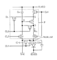
- FIG. 10 illustrates a second embodiment of a second sub-pixel SPb including the coupling capacitor Cc.
- the second sub-pixel SPb of this embodiment includes a pixel circuit P, a second light-emitting device OLEDb, and a second initialization circuit IC_b.
- the first driving voltage ELVDD is supplied to the pixel circuit P.
- a data line DL, a second control line CL 2 , a third control line CL 3 , and a fourth control line CL 4 are connected to the pixel circuit P.
- a data signal is supplied to the pixel circuit P through the data line DL, a second control signal is supplied to the pixel circuit P through the second control line CL 2 , a third control signal is supplied to the pixel circuit P through the third control line CL 3 , and a fourth control signal is supplied to the pixel circuit P through the fourth control line CL 4 .
- the second control signal and the third control signal may be sequentially supplied to the pixel circuit P through the second control line CL 2 and the third control line CL 3 , respectively.
- the pixel circuit P includes a driving transistor T 1 and a switching transistor T 2 .
- the driving transistor T 1 includes a first electrode receiving the first driving voltage ELVDD and a second electrode connected to the second light-emitting device OLEDb.
- the switching transistor T 2 includes a first electrode receiving a data signal and a second electrode connected to the first electrode of the driving transistor T 1 .
- the driving transistor T 1 may supply a driving current IEL corresponding to the size of a voltage of the data signal to the second light-emitting device OLEDb according to a switching operation of the switching transistor T 2 .
- the pixel circuit P may further include a gate initialization transistor T 4 , a compensation transistor T 3 , light-emitting control transistors T 5 and T 6 , and a storage capacitor Cst.
- the gate initialization transistor T 4 may include a gate electrode connected to the second control line CL 2 , a first electrode to which an initial voltage Vinit is applied, and a second electrode connected to a gate electrode of the driving transistor T 1 .
- the gate initialization transistor T 4 may supply the initial voltage Vinit to the gate electrode of the driving transistor T 1 in response to the second control signal supplied through the second control line CL 2 .
- the compensation transistor T 3 may include a gate electrode connected to the third control line CL 3 , a first electrode connected to the gate electrode of the driving transistor T 1 , and a second electrode connected to the second electrode of the driving transistor T 1 .
- the compensation transistor T 3 may connect the gate electrode of the driving transistor T 1 to the second electrode thereof in response to the third control signal supplied through the third control line CL 3 , so that the driving transistor T 1 is placed in a diode-connected state.
- the light-emitting control transistors T 5 and T 6 may include at least one of a first light-emitting control transistor T 5 , which connects the driving transistor T 1 and a line through which the first driving voltage ELVDD is supplied, or a second light-emitting transistor T 6 that connects the driving transistor T 1 and the second light-emitting device OLEDb.
- the first light-emitting control transistor T 5 may include a gate electrode connected to the fourth control line CL 4 , a first electrode connected to the line through which the first driving voltage ELVDD is supplied, and a second electrode connected to the first electrode of the driving transistor T 1 .
- the second light-emitting control transistor T 6 may include a gate electrode connected to the fourth control line CL 4 , a first electrode connected to the second electrode of the driving transistor T 1 , and a second electrode connected to an anode electrode of the second light-emitting device OLEDb.
- the light-emitting control transistors T 5 and T 6 may output the driving current IEL to an output node Node_out in response to the fourth control signal supplied through the fourth control line CL 4 .
- the first light-emitting control transistor T 5 and/or the second light-emitting control transistor T 6 are turned on in response to the fourth control signal supplied through the fourth control line CL 4 .
- the driving current IEL flows to the second light-emitting device OLEDb.
- the storage capacitor Cst is connected between the line through which the first driving voltage ELVDD is supplied and a gate node G of the driving transistor T 1 .
- a voltage difference between the first driving voltage ELVDD and a voltage of the gate node G of the driving transistor T 1 may be stored in the storage capacitor Cst.
- the second initialization circuit IC_b includes an anode initialization transistor T 7 and the coupling capacitor Cc.
- a gate electrode of the anode initialization transistor T 7 is connected to the first control line CL 1
- a first electrode of the anode initialization transistor T 7 is connected to the anode of the second light-emitting device OLEDb.
- a second electrode of the anode initialization transistor T 7 is connected to a line through which the initial voltage Vinit is supplied.
- the anode initialization transistor T 7 is turned on in response to the first control signal supplied from the first control line CL 1 , and initializes an anode voltage Vanode_b of the second light-emitting device OLEDb.
- the anode voltage Vanode_b of the second light-emitting device OLEDb drops to the level of the initial voltage Vinit in synchronization with a falling edge of the first control signal supplied through the first control line CL 1 .
- the anode initialization transistor T 7 is turned on in response to a falling edge of the first control signal.
- the initial voltage Vinit is applied to the output node Node_out.
- the anode voltage Vanode_b rises in synchronization with a rising edge of the first control signal.
- the coupling capacitor Cc is connected between the first control line CL 1 and the output node Node_out.
- the electric potential of the output node Node_out also varies by the coupling capacitor Cc. Accordingly, when the first control signal transmitted through the first control line CL 1 transitions from a low level to a high level, the electric potential of the output node Node_out also rises by the coupling capacitor Cc.
- the second control signal having a low level is supplied through the second control line CL 2 .
- the gate initialization transistor T 4 is turned on.
- the initial voltage Vinit is transferred to the gate electrode of the driving transistor T 1 through the gate initialization transistor T 4 .
- a gate voltage of the driving transistor T 1 is initialized.
- the third control signal having a low level is supplied through the third control line CL 3 .
- the switching transistor T 2 and the compensation transistor T 3 are turned on.
- the switching transistor T 2 transfers a data signal received through the data line DL to the first electrode of the driving transistor T 1 .
- a compensation voltage VD+Vth (where Vth is a negative value), obtained by subtracting a threshold voltage Vth of the driving transistor T 1 from a voltage VD of the data signal, is applied to the gate electrode of the driving transistor T 1 .
- the first driving voltage ELVDD is applied to one terminal of the storage capacitor Cst and the compensation voltage VD+Vth is applied to the other terminal of the storage capacitor Cst.
- the storage capacitor Cst is charged with electric charges corresponding to a voltage difference ELVDD ⁇ (VD+Vth) between both terminals of the storage capacitor Cst.
- the anode initialization transistor T 7 is turned on and the anode voltage Vanode of the second light-emitting device OLEDb lowers up to the level of the initial voltage Vinit.
- the voltage of the initialization control signal is applied to one terminal of the coupling capacitor Cc, and the anode voltage Vanode of the second light-emitting device OLEDb is applied to the other terminal of the coupling capacitor Cc.
- the coupling capacitor Cc is charged with electric charges corresponding to a voltage difference between both terminals of the coupling capacitor Cc.
- the anode initialization transistor T 7 When the first control signal having a high level is supplied through the first control line CL 1 , the anode initialization transistor T 7 is turned off and the anode voltage Vanode of the second light-emitting device OLEDb rises in synchronization with a rising edge of the initialization control signal.
- the fourth control signal that is supplied from the fourth control line CL 4 falls from a high level to a low level and the first light-emitting transistor T 5 and the second light-emitting transistor T 6 are turned on.
- the driving current IEL is generated according to a voltage difference between a voltage of the gate electrode of the driving transistor T 1 and the first driving voltage ELVDD and is supplied to the second light-emitting device OLEDb through the second light-emitting control transistor T 6 , and the second light-emitting device OLEDb may emit light by the driving current IEL.
- the coupling capacitor Cc may raise the anode voltage Vanode of the second light-emitting device OLEDb before the light-emitting period, to thereby bring a light-emitting time point of the second sub-pixel SPb forward.
- color spreading occurs when the expression of a specific color of light of pixel, or sub-pixel, is insufficient compared to the expression of another color of light of a pixel, or sub-pixel.
- the threshold voltage of a light-emitting device of a green sub-pixel may be higher than the light-emitting device of a red or blue sub-pixel.
- the amount of driving current of the light-emitting device of the green pixel sub-pixel may be less than the amount of driving current of a light-emitting device of another color sub-pixel.
- the time taken until the light-emitting device of the green sub-pixel emits light may be longer than the time taken until the light-emitting device of the red or blue sub-pixel emits light.
- a color spreading phenomenon in which the green color is seen as a purple color may occur.
- an organic light-emitting display apparatus in which operation timings of sub-pixels that emit different colors of light may coincide with each other.
- a color spreading may be reduced or removed.
- the green sub-pixel may be coupled to a capacitor for reducing color spreading.
Landscapes
- Engineering & Computer Science (AREA)
- Physics & Mathematics (AREA)
- Computer Hardware Design (AREA)
- General Physics & Mathematics (AREA)
- Theoretical Computer Science (AREA)
- Control Of El Displays (AREA)
- Control Of Indicators Other Than Cathode Ray Tubes (AREA)
- Multimedia (AREA)
- Electroluminescent Light Sources (AREA)
Applications Claiming Priority (2)
| Application Number | Priority Date | Filing Date | Title |
|---|---|---|---|
| KR1020140073677A KR102194825B1 (ko) | 2014-06-17 | 2014-06-17 | 유기 발광 표시 장치 |
| KR10-2014-0073677 | 2014-06-17 |
Publications (2)
| Publication Number | Publication Date |
|---|---|
| US20150364092A1 US20150364092A1 (en) | 2015-12-17 |
| US9805651B2 true US9805651B2 (en) | 2017-10-31 |
Family
ID=54836647
Family Applications (1)
| Application Number | Title | Priority Date | Filing Date |
|---|---|---|---|
| US14/657,219 Active 2035-05-01 US9805651B2 (en) | 2014-06-17 | 2015-03-13 | Organic light emitting display apparatus |
Country Status (2)
| Country | Link |
|---|---|
| US (1) | US9805651B2 (ko) |
| KR (1) | KR102194825B1 (ko) |
Cited By (7)
| Publication number | Priority date | Publication date | Assignee | Title |
|---|---|---|---|---|
| US10839757B2 (en) | 2018-09-17 | 2020-11-17 | Samsung Display Co., Ltd. | Display device |
| US10885842B2 (en) | 2018-07-17 | 2021-01-05 | Samsung Display Co., Ltd. | Display device and a method of driving the same |
| US11030939B2 (en) | 2018-04-12 | 2021-06-08 | Samsung Display Co., Ltd. | Display device |
| US11081049B2 (en) | 2018-12-28 | 2021-08-03 | Samsung Display Co., Ltd. | Pixel and display device having the same |
| US11088215B2 (en) | 2019-05-16 | 2021-08-10 | Samsung Display Co., Ltd. | Organic light-emitting display apparatus |
| US11145253B2 (en) | 2018-07-09 | 2021-10-12 | Samsung Display Co., Ltd. | Display device and method of driving the same |
| US11151948B2 (en) | 2018-06-26 | 2021-10-19 | Samsung Display Co., Ltd. | Organic light emitting display device and method for driving the same |
Families Citing this family (13)
| Publication number | Priority date | Publication date | Assignee | Title |
|---|---|---|---|---|
| KR102551789B1 (ko) | 2016-06-15 | 2023-07-07 | 삼성디스플레이 주식회사 | 디스플레이 장치 |
| KR102622312B1 (ko) * | 2016-12-19 | 2024-01-10 | 삼성디스플레이 주식회사 | 표시장치 및 그의 구동방법 |
| CN108806608B (zh) * | 2018-06-12 | 2020-06-02 | 京东方科技集团股份有限公司 | 一种驱动晶体管的阈值电压侦测方法及装置、显示装置 |
| KR102540994B1 (ko) | 2018-07-06 | 2023-06-08 | 삼성디스플레이 주식회사 | 화소 및 이를 포함하는 표시 장치 |
| KR102662937B1 (ko) * | 2018-09-17 | 2024-05-08 | 삼성디스플레이 주식회사 | 표시 장치 |
| KR102570985B1 (ko) * | 2018-11-06 | 2023-08-29 | 삼성디스플레이 주식회사 | 화소 회로 |
| KR102588103B1 (ko) * | 2018-11-16 | 2023-10-11 | 엘지디스플레이 주식회사 | 표시 장치 |
| CN109523954B (zh) * | 2018-12-24 | 2020-12-22 | 合肥鑫晟光电科技有限公司 | 像素单元、显示面板、驱动方法以及补偿控制方法 |
| KR20220023176A (ko) * | 2020-08-20 | 2022-03-02 | 엘지디스플레이 주식회사 | 픽셀 회로와 이를 이용한 표시장치 |
| CN112037716B (zh) * | 2020-09-21 | 2022-01-21 | 京东方科技集团股份有限公司 | 像素电路、显示面板和显示设备 |
| CN112908258B (zh) * | 2021-03-23 | 2022-10-21 | 武汉天马微电子有限公司 | 像素驱动电路、驱动方法、显示面板与显示装置 |
| CN114464134B (zh) * | 2022-03-30 | 2023-09-05 | 京东方科技集团股份有限公司 | 像素电路及显示装置 |
| CN117813644A (zh) * | 2022-07-08 | 2024-04-02 | 京东方科技集团股份有限公司 | 显示面板及显示装置 |
Citations (5)
| Publication number | Priority date | Publication date | Assignee | Title |
|---|---|---|---|---|
| US20080316150A1 (en) * | 2007-06-21 | 2008-12-25 | Samsung Sdi Co., Ltd. | Organic light emitting diode display device |
| US20130009933A1 (en) * | 2011-07-07 | 2013-01-10 | Sony Corporation | Pixel circuit, display device, electronic apparatus, and method of driving pixel circuit |
| US20130201172A1 (en) | 2012-02-07 | 2013-08-08 | Samsung Display Co., Ltd. | Pixel and organic light emitting diode display using the same |
| US20130286054A1 (en) | 2012-04-25 | 2013-10-31 | Seiko Epson Corporation | Electro-optical device and electronic apparatus |
| KR20130136554A (ko) | 2011-08-09 | 2013-12-12 | 파나소닉 주식회사 | 화상 표시 장치의 구동 방법 |
Family Cites Families (5)
| Publication number | Priority date | Publication date | Assignee | Title |
|---|---|---|---|---|
| JP4884701B2 (ja) * | 2004-05-21 | 2012-02-29 | 株式会社半導体エネルギー研究所 | 表示装置 |
| JP2009288767A (ja) * | 2008-05-01 | 2009-12-10 | Sony Corp | 表示装置及びその駆動方法 |
| KR101498094B1 (ko) * | 2008-09-29 | 2015-03-05 | 삼성디스플레이 주식회사 | 표시 장치 및 그 구동 방법 |
| KR101152580B1 (ko) * | 2010-06-30 | 2012-06-01 | 삼성모바일디스플레이주식회사 | 화소 및 이를 이용한 유기전계발광 표시장치 |
| KR102097473B1 (ko) * | 2013-11-29 | 2020-04-07 | 삼성디스플레이 주식회사 | 화소 및 이를 이용한 유기전계발광 표시장치 |
-
2014
- 2014-06-17 KR KR1020140073677A patent/KR102194825B1/ko active IP Right Grant
-
2015
- 2015-03-13 US US14/657,219 patent/US9805651B2/en active Active
Patent Citations (8)
| Publication number | Priority date | Publication date | Assignee | Title |
|---|---|---|---|---|
| US20080316150A1 (en) * | 2007-06-21 | 2008-12-25 | Samsung Sdi Co., Ltd. | Organic light emitting diode display device |
| US20130009933A1 (en) * | 2011-07-07 | 2013-01-10 | Sony Corporation | Pixel circuit, display device, electronic apparatus, and method of driving pixel circuit |
| KR20130136554A (ko) | 2011-08-09 | 2013-12-12 | 파나소닉 주식회사 | 화상 표시 장치의 구동 방법 |
| US20140022288A1 (en) | 2011-08-09 | 2014-01-23 | Panasonic Corporation | Driving method of display apparatus |
| US20130201172A1 (en) | 2012-02-07 | 2013-08-08 | Samsung Display Co., Ltd. | Pixel and organic light emitting diode display using the same |
| KR20130091136A (ko) | 2012-02-07 | 2013-08-16 | 삼성디스플레이 주식회사 | 화소 및 이를 이용한 유기 발광 표시 장치 |
| US20130286054A1 (en) | 2012-04-25 | 2013-10-31 | Seiko Epson Corporation | Electro-optical device and electronic apparatus |
| KR20130120402A (ko) | 2012-04-25 | 2013-11-04 | 세이코 엡슨 가부시키가이샤 | 전기 광학 장치 및 전자 기기 |
Cited By (9)
| Publication number | Priority date | Publication date | Assignee | Title |
|---|---|---|---|---|
| US11030939B2 (en) | 2018-04-12 | 2021-06-08 | Samsung Display Co., Ltd. | Display device |
| US11417268B2 (en) | 2018-04-12 | 2022-08-16 | Samsung Display Co., Ltd. | Display device |
| US11151948B2 (en) | 2018-06-26 | 2021-10-19 | Samsung Display Co., Ltd. | Organic light emitting display device and method for driving the same |
| US11145253B2 (en) | 2018-07-09 | 2021-10-12 | Samsung Display Co., Ltd. | Display device and method of driving the same |
| US10885842B2 (en) | 2018-07-17 | 2021-01-05 | Samsung Display Co., Ltd. | Display device and a method of driving the same |
| US10839757B2 (en) | 2018-09-17 | 2020-11-17 | Samsung Display Co., Ltd. | Display device |
| US11164533B2 (en) | 2018-09-17 | 2021-11-02 | Samsung Display Co. Ltd. | Display device |
| US11081049B2 (en) | 2018-12-28 | 2021-08-03 | Samsung Display Co., Ltd. | Pixel and display device having the same |
| US11088215B2 (en) | 2019-05-16 | 2021-08-10 | Samsung Display Co., Ltd. | Organic light-emitting display apparatus |
Also Published As
| Publication number | Publication date |
|---|---|
| KR102194825B1 (ko) | 2020-12-24 |
| US20150364092A1 (en) | 2015-12-17 |
| KR20150144893A (ko) | 2015-12-29 |
Similar Documents
| Publication | Publication Date | Title |
|---|---|---|
| US9805651B2 (en) | Organic light emitting display apparatus | |
| US9721508B2 (en) | Pixel circuit and driving method thereof, organic light-emitting display device | |
| EP3001405B1 (en) | Organic light-emitting diode display device and method for driving the same | |
| US10339862B2 (en) | Pixel and organic light emitting display device using the same | |
| US10068527B2 (en) | Light-emitting display apparatus and driving method thereof | |
| US10043441B2 (en) | Pixel, organic light emitting display device, and driving method thereof | |
| US10777145B2 (en) | Demultiplexer, display device including the same, and method of driving the display device | |
| US8138997B2 (en) | Pixel, organic light emitting display using the same, and associated methods | |
| CN106448557B (zh) | 发光驱动电路及有机发光显示器 | |
| US9747843B2 (en) | Display apparatus having de-multiplexer and driving method thereof | |
| KR102345665B1 (ko) | 표시장치 및 그의 구동방법 | |
| KR20170132016A (ko) | Oled 표시 장치 및 그의 구동 방법 | |
| US11696475B2 (en) | Display device including a fifth transistor connected between the power line and the light emitting diode | |
| US10504433B2 (en) | Pixel and organic light emitting display device including the same | |
| KR20140124535A (ko) | 화소 및 이를 이용한 유기전계발광 표시장치 | |
| CN110060638B (zh) | Amoled电压编程像素电路及其驱动方法 | |
| KR102424978B1 (ko) | 유기 발광 표시 장치 | |
| KR20140117121A (ko) | 유기발광 표시장치 | |
| US20150022514A1 (en) | Organic light emitting display device | |
| KR102675922B1 (ko) | 픽셀 회로 및 이를 포함하는 유기 발광 표시 장치 | |
| KR20140114213A (ko) | 유기전계발광표시장치와 이의 구동방법 | |
| KR101375059B1 (ko) | 화소회로, 표시패널 및 이를 구비한 표시장치 | |
| KR20200075488A (ko) | 픽셀 회로와 이를 이용한 전계 발광 표시장치 | |
| KR20230095243A (ko) | 유기 발광 표시 장치 |
Legal Events
| Date | Code | Title | Description |
|---|---|---|---|
| AS | Assignment |
Owner name: SAMSUNG DISPLAY CO., LTD., KOREA, REPUBLIC OF Free format text: ASSIGNMENT OF ASSIGNORS INTEREST;ASSIGNOR:KIM, YANG-WAN;REEL/FRAME:035162/0586 Effective date: 20150303 |
|
| STCF | Information on status: patent grant |
Free format text: PATENTED CASE |
|
| MAFP | Maintenance fee payment |
Free format text: PAYMENT OF MAINTENANCE FEE, 4TH YEAR, LARGE ENTITY (ORIGINAL EVENT CODE: M1551); ENTITY STATUS OF PATENT OWNER: LARGE ENTITY Year of fee payment: 4 |