US9793358B2 - Non-planar semiconductor device with multiple-head epitaxial structure on fin - Google Patents
Non-planar semiconductor device with multiple-head epitaxial structure on fin Download PDFInfo
- Publication number
- US9793358B2 US9793358B2 US14/267,541 US201414267541A US9793358B2 US 9793358 B2 US9793358 B2 US 9793358B2 US 201414267541 A US201414267541 A US 201414267541A US 9793358 B2 US9793358 B2 US 9793358B2
- Authority
- US
- United States
- Prior art keywords
- epitaxial
- raised
- structures
- epitaxial structure
- semiconductor structure
- Prior art date
- Legal status (The legal status is an assumption and is not a legal conclusion. Google has not performed a legal analysis and makes no representation as to the accuracy of the status listed.)
- Active, expires
Links
- 239000004065 semiconductor Substances 0.000 title claims abstract description 57
- 239000000463 material Substances 0.000 claims abstract description 59
- 239000010703 silicon Substances 0.000 claims abstract description 12
- 229910052710 silicon Inorganic materials 0.000 claims abstract description 12
- 239000000758 substrate Substances 0.000 claims description 10
- 229910000577 Silicon-germanium Inorganic materials 0.000 claims description 3
- LEVVHYCKPQWKOP-UHFFFAOYSA-N [Si].[Ge] Chemical compound [Si].[Ge] LEVVHYCKPQWKOP-UHFFFAOYSA-N 0.000 claims description 3
- 230000000737 periodic effect Effects 0.000 claims description 3
- 229910052732 germanium Inorganic materials 0.000 claims description 2
- GNPVGFCGXDBREM-UHFFFAOYSA-N germanium atom Chemical compound [Ge] GNPVGFCGXDBREM-UHFFFAOYSA-N 0.000 claims description 2
- 239000000945 filler Substances 0.000 abstract description 46
- XUIMIQQOPSSXEZ-UHFFFAOYSA-N Silicon Chemical compound [Si] XUIMIQQOPSSXEZ-UHFFFAOYSA-N 0.000 abstract description 11
- 229910003460 diamond Inorganic materials 0.000 abstract description 2
- 239000010432 diamond Substances 0.000 abstract description 2
- 238000012986 modification Methods 0.000 abstract description 2
- 230000004048 modification Effects 0.000 abstract description 2
- 239000010410 layer Substances 0.000 description 34
- 239000011241 protective layer Substances 0.000 description 17
- 230000001681 protective effect Effects 0.000 description 15
- 238000005530 etching Methods 0.000 description 11
- 238000000034 method Methods 0.000 description 11
- 238000000151 deposition Methods 0.000 description 7
- 150000004767 nitrides Chemical class 0.000 description 7
- 238000000231 atomic layer deposition Methods 0.000 description 4
- 238000000623 plasma-assisted chemical vapour deposition Methods 0.000 description 4
- 230000008569 process Effects 0.000 description 4
- 230000008021 deposition Effects 0.000 description 3
- 238000000407 epitaxy Methods 0.000 description 3
- 230000006870 function Effects 0.000 description 3
- 238000004519 manufacturing process Methods 0.000 description 3
- 230000000873 masking effect Effects 0.000 description 3
- 239000000126 substance Substances 0.000 description 3
- QGZKDVFQNNGYKY-UHFFFAOYSA-N Ammonia Chemical compound N QGZKDVFQNNGYKY-UHFFFAOYSA-N 0.000 description 2
- 238000005498 polishing Methods 0.000 description 2
- WGTYBPLFGIVFAS-UHFFFAOYSA-M tetramethylammonium hydroxide Chemical compound [OH-].C[N+](C)(C)C WGTYBPLFGIVFAS-UHFFFAOYSA-M 0.000 description 2
- 238000007792 addition Methods 0.000 description 1
- 229910021529 ammonia Inorganic materials 0.000 description 1
- 230000008859 change Effects 0.000 description 1
- -1 for example Substances 0.000 description 1
- 238000002955 isolation Methods 0.000 description 1
- 238000004943 liquid phase epitaxy Methods 0.000 description 1
- 238000001459 lithography Methods 0.000 description 1
- 238000001451 molecular beam epitaxy Methods 0.000 description 1
- 238000006467 substitution reaction Methods 0.000 description 1
- 238000000927 vapour-phase epitaxy Methods 0.000 description 1
Images


Classifications
-
- H—ELECTRICITY
- H01—ELECTRIC ELEMENTS
- H01L—SEMICONDUCTOR DEVICES NOT COVERED BY CLASS H10
- H01L29/00—Semiconductor devices adapted for rectifying, amplifying, oscillating or switching, or capacitors or resistors with at least one potential-jump barrier or surface barrier, e.g. PN junction depletion layer or carrier concentration layer; Details of semiconductor bodies or of electrodes thereof ; Multistep manufacturing processes therefor
- H01L29/02—Semiconductor bodies ; Multistep manufacturing processes therefor
- H01L29/12—Semiconductor bodies ; Multistep manufacturing processes therefor characterised by the materials of which they are formed
- H01L29/16—Semiconductor bodies ; Multistep manufacturing processes therefor characterised by the materials of which they are formed including, apart from doping materials or other impurities, only elements of Group IV of the Periodic System
- H01L29/161—Semiconductor bodies ; Multistep manufacturing processes therefor characterised by the materials of which they are formed including, apart from doping materials or other impurities, only elements of Group IV of the Periodic System including two or more of the elements provided for in group H01L29/16, e.g. alloys
-
- H—ELECTRICITY
- H01—ELECTRIC ELEMENTS
- H01L—SEMICONDUCTOR DEVICES NOT COVERED BY CLASS H10
- H01L21/00—Processes or apparatus adapted for the manufacture or treatment of semiconductor or solid state devices or of parts thereof
- H01L21/02—Manufacture or treatment of semiconductor devices or of parts thereof
- H01L21/02104—Forming layers
- H01L21/02365—Forming inorganic semiconducting materials on a substrate
- H01L21/02367—Substrates
- H01L21/0237—Materials
- H01L21/02373—Group 14 semiconducting materials
- H01L21/02381—Silicon, silicon germanium, germanium
-
- H—ELECTRICITY
- H01—ELECTRIC ELEMENTS
- H01L—SEMICONDUCTOR DEVICES NOT COVERED BY CLASS H10
- H01L21/00—Processes or apparatus adapted for the manufacture or treatment of semiconductor or solid state devices or of parts thereof
- H01L21/02—Manufacture or treatment of semiconductor devices or of parts thereof
- H01L21/02104—Forming layers
- H01L21/02365—Forming inorganic semiconducting materials on a substrate
- H01L21/02367—Substrates
- H01L21/02428—Structure
- H01L21/0243—Surface structure
-
- H—ELECTRICITY
- H01—ELECTRIC ELEMENTS
- H01L—SEMICONDUCTOR DEVICES NOT COVERED BY CLASS H10
- H01L21/00—Processes or apparatus adapted for the manufacture or treatment of semiconductor or solid state devices or of parts thereof
- H01L21/02—Manufacture or treatment of semiconductor devices or of parts thereof
- H01L21/02104—Forming layers
- H01L21/02365—Forming inorganic semiconducting materials on a substrate
- H01L21/02518—Deposited layers
- H01L21/02521—Materials
- H01L21/02524—Group 14 semiconducting materials
- H01L21/02532—Silicon, silicon germanium, germanium
-
- H—ELECTRICITY
- H01—ELECTRIC ELEMENTS
- H01L—SEMICONDUCTOR DEVICES NOT COVERED BY CLASS H10
- H01L21/00—Processes or apparatus adapted for the manufacture or treatment of semiconductor or solid state devices or of parts thereof
- H01L21/02—Manufacture or treatment of semiconductor devices or of parts thereof
- H01L21/02104—Forming layers
- H01L21/02365—Forming inorganic semiconducting materials on a substrate
- H01L21/02518—Deposited layers
- H01L21/02587—Structure
- H01L21/0259—Microstructure
-
- H—ELECTRICITY
- H01—ELECTRIC ELEMENTS
- H01L—SEMICONDUCTOR DEVICES NOT COVERED BY CLASS H10
- H01L21/00—Processes or apparatus adapted for the manufacture or treatment of semiconductor or solid state devices or of parts thereof
- H01L21/02—Manufacture or treatment of semiconductor devices or of parts thereof
- H01L21/02104—Forming layers
- H01L21/02365—Forming inorganic semiconducting materials on a substrate
- H01L21/02612—Formation types
- H01L21/02617—Deposition types
- H01L21/02636—Selective deposition, e.g. simultaneous growth of mono- and non-monocrystalline semiconductor materials
- H01L21/02639—Preparation of substrate for selective deposition
-
- H—ELECTRICITY
- H01—ELECTRIC ELEMENTS
- H01L—SEMICONDUCTOR DEVICES NOT COVERED BY CLASS H10
- H01L21/00—Processes or apparatus adapted for the manufacture or treatment of semiconductor or solid state devices or of parts thereof
- H01L21/02—Manufacture or treatment of semiconductor devices or of parts thereof
- H01L21/02104—Forming layers
- H01L21/02365—Forming inorganic semiconducting materials on a substrate
- H01L21/02656—Special treatments
- H01L21/02664—Aftertreatments
-
- H—ELECTRICITY
- H01—ELECTRIC ELEMENTS
- H01L—SEMICONDUCTOR DEVICES NOT COVERED BY CLASS H10
- H01L21/00—Processes or apparatus adapted for the manufacture or treatment of semiconductor or solid state devices or of parts thereof
- H01L21/70—Manufacture or treatment of devices consisting of a plurality of solid state components formed in or on a common substrate or of parts thereof; Manufacture of integrated circuit devices or of parts thereof
- H01L21/77—Manufacture or treatment of devices consisting of a plurality of solid state components or integrated circuits formed in, or on, a common substrate
- H01L21/78—Manufacture or treatment of devices consisting of a plurality of solid state components or integrated circuits formed in, or on, a common substrate with subsequent division of the substrate into plural individual devices
- H01L21/82—Manufacture or treatment of devices consisting of a plurality of solid state components or integrated circuits formed in, or on, a common substrate with subsequent division of the substrate into plural individual devices to produce devices, e.g. integrated circuits, each consisting of a plurality of components
- H01L21/822—Manufacture or treatment of devices consisting of a plurality of solid state components or integrated circuits formed in, or on, a common substrate with subsequent division of the substrate into plural individual devices to produce devices, e.g. integrated circuits, each consisting of a plurality of components the substrate being a semiconductor, using silicon technology
- H01L21/8232—Field-effect technology
- H01L21/8234—MIS technology, i.e. integration processes of field effect transistors of the conductor-insulator-semiconductor type
- H01L21/823431—MIS technology, i.e. integration processes of field effect transistors of the conductor-insulator-semiconductor type with a particular manufacturing method of transistors with a horizontal current flow in a vertical sidewall of a semiconductor body, e.g. FinFET, MuGFET
-
- H—ELECTRICITY
- H01—ELECTRIC ELEMENTS
- H01L—SEMICONDUCTOR DEVICES NOT COVERED BY CLASS H10
- H01L27/00—Devices consisting of a plurality of semiconductor or other solid-state components formed in or on a common substrate
- H01L27/02—Devices consisting of a plurality of semiconductor or other solid-state components formed in or on a common substrate including semiconductor components specially adapted for rectifying, oscillating, amplifying or switching and having at least one potential-jump barrier or surface barrier; including integrated passive circuit elements with at least one potential-jump barrier or surface barrier
- H01L27/04—Devices consisting of a plurality of semiconductor or other solid-state components formed in or on a common substrate including semiconductor components specially adapted for rectifying, oscillating, amplifying or switching and having at least one potential-jump barrier or surface barrier; including integrated passive circuit elements with at least one potential-jump barrier or surface barrier the substrate being a semiconductor body
- H01L27/08—Devices consisting of a plurality of semiconductor or other solid-state components formed in or on a common substrate including semiconductor components specially adapted for rectifying, oscillating, amplifying or switching and having at least one potential-jump barrier or surface barrier; including integrated passive circuit elements with at least one potential-jump barrier or surface barrier the substrate being a semiconductor body including only semiconductor components of a single kind
- H01L27/085—Devices consisting of a plurality of semiconductor or other solid-state components formed in or on a common substrate including semiconductor components specially adapted for rectifying, oscillating, amplifying or switching and having at least one potential-jump barrier or surface barrier; including integrated passive circuit elements with at least one potential-jump barrier or surface barrier the substrate being a semiconductor body including only semiconductor components of a single kind including field-effect components only
- H01L27/088—Devices consisting of a plurality of semiconductor or other solid-state components formed in or on a common substrate including semiconductor components specially adapted for rectifying, oscillating, amplifying or switching and having at least one potential-jump barrier or surface barrier; including integrated passive circuit elements with at least one potential-jump barrier or surface barrier the substrate being a semiconductor body including only semiconductor components of a single kind including field-effect components only the components being field-effect transistors with insulated gate
- H01L27/0886—Devices consisting of a plurality of semiconductor or other solid-state components formed in or on a common substrate including semiconductor components specially adapted for rectifying, oscillating, amplifying or switching and having at least one potential-jump barrier or surface barrier; including integrated passive circuit elements with at least one potential-jump barrier or surface barrier the substrate being a semiconductor body including only semiconductor components of a single kind including field-effect components only the components being field-effect transistors with insulated gate including transistors with a horizontal current flow in a vertical sidewall of a semiconductor body, e.g. FinFET, MuGFET
-
- H—ELECTRICITY
- H01—ELECTRIC ELEMENTS
- H01L—SEMICONDUCTOR DEVICES NOT COVERED BY CLASS H10
- H01L29/00—Semiconductor devices adapted for rectifying, amplifying, oscillating or switching, or capacitors or resistors with at least one potential-jump barrier or surface barrier, e.g. PN junction depletion layer or carrier concentration layer; Details of semiconductor bodies or of electrodes thereof ; Multistep manufacturing processes therefor
- H01L29/02—Semiconductor bodies ; Multistep manufacturing processes therefor
- H01L29/06—Semiconductor bodies ; Multistep manufacturing processes therefor characterised by their shape; characterised by the shapes, relative sizes, or dispositions of the semiconductor regions ; characterised by the concentration or distribution of impurities within semiconductor regions
- H01L29/0657—Semiconductor bodies ; Multistep manufacturing processes therefor characterised by their shape; characterised by the shapes, relative sizes, or dispositions of the semiconductor regions ; characterised by the concentration or distribution of impurities within semiconductor regions characterised by the shape of the body
-
- H—ELECTRICITY
- H01—ELECTRIC ELEMENTS
- H01L—SEMICONDUCTOR DEVICES NOT COVERED BY CLASS H10
- H01L29/00—Semiconductor devices adapted for rectifying, amplifying, oscillating or switching, or capacitors or resistors with at least one potential-jump barrier or surface barrier, e.g. PN junction depletion layer or carrier concentration layer; Details of semiconductor bodies or of electrodes thereof ; Multistep manufacturing processes therefor
- H01L29/66—Types of semiconductor device ; Multistep manufacturing processes therefor
- H01L29/66007—Multistep manufacturing processes
- H01L29/66075—Multistep manufacturing processes of devices having semiconductor bodies comprising group 14 or group 13/15 materials
- H01L29/66227—Multistep manufacturing processes of devices having semiconductor bodies comprising group 14 or group 13/15 materials the devices being controllable only by the electric current supplied or the electric potential applied, to an electrode which does not carry the current to be rectified, amplified or switched, e.g. three-terminal devices
- H01L29/66409—Unipolar field-effect transistors
- H01L29/66477—Unipolar field-effect transistors with an insulated gate, i.e. MISFET
- H01L29/66787—Unipolar field-effect transistors with an insulated gate, i.e. MISFET with a gate at the side of the channel
- H01L29/66795—Unipolar field-effect transistors with an insulated gate, i.e. MISFET with a gate at the side of the channel with a horizontal current flow in a vertical sidewall of a semiconductor body, e.g. FinFET, MuGFET
-
- H—ELECTRICITY
- H01—ELECTRIC ELEMENTS
- H01L—SEMICONDUCTOR DEVICES NOT COVERED BY CLASS H10
- H01L29/00—Semiconductor devices adapted for rectifying, amplifying, oscillating or switching, or capacitors or resistors with at least one potential-jump barrier or surface barrier, e.g. PN junction depletion layer or carrier concentration layer; Details of semiconductor bodies or of electrodes thereof ; Multistep manufacturing processes therefor
- H01L29/66—Types of semiconductor device ; Multistep manufacturing processes therefor
- H01L29/68—Types of semiconductor device ; Multistep manufacturing processes therefor controllable by only the electric current supplied, or only the electric potential applied, to an electrode which does not carry the current to be rectified, amplified or switched
- H01L29/76—Unipolar devices, e.g. field effect transistors
- H01L29/772—Field effect transistors
- H01L29/78—Field effect transistors with field effect produced by an insulated gate
- H01L29/785—Field effect transistors with field effect produced by an insulated gate having a channel with a horizontal current flow in a vertical sidewall of a semiconductor body, e.g. FinFET, MuGFET
- H01L29/7853—Field effect transistors with field effect produced by an insulated gate having a channel with a horizontal current flow in a vertical sidewall of a semiconductor body, e.g. FinFET, MuGFET the body having a non-rectangular crossection
Definitions
- the present invention generally relates to non-planar semiconductor structures with epitaxial structures on top surfaces of raised semiconductor structures. More specifically, the present invention relates to increasing the surface area of the epitaxial structures without adding additional epitaxial material.
- the shortcomings of the prior art are overcome and additional advantages are provided through the provision, in one aspect, of a method of fabricating a non-planar semiconductor structure with multiple epitaxial heads.
- the method includes providing a starting non-planar semiconductor structure, the structure including a semiconductor substrate and at least one raised semiconductor structure coupled to the substrate.
- the method further includes growing at least one epitaxial structure on a top surface of one or more of the at least one raised semiconductor structure, the at least one epitaxial structure having a surface area, and increasing the surface area of the at least one epitaxial structure without growing additional epitaxy.
- a non-planar semiconductor structure includes a semiconductor substrate, at least one raised semiconductor structure coupled to the substrate, and at least one epitaxial structure grown on a partially recessed top surface of one or more of the at least one raised semiconductor structure, the at least one epitaxial structure including at least two epitaxial head structures joined together at a common base of the at least one epitaxial structure.
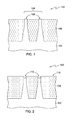
- FIG. 1 depicts one example of a starting non-planar semiconductor structure in accordance with one or more aspects of the present invention.
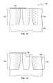
- FIG. 2 depicts one example of the structure of FIG. 1 after recessing the raised structures below the layer of filler material in accordance with one or more aspects of the present invention.
- FIG. 3 depicts one example of the structure of FIG. 2 after growing epitaxial structures on top surfaces of the raised structures in accordance with one or more aspects of the present invention.
- FIG. 4 depicts one example of the structure of FIG. 3 after deposition of a blanket layer of protective material in accordance with one or more aspects of the present invention.
- FIG. 5 depicts one example of the structure of FIG. 4 after conformal deposition of the filler material over the protective layer in accordance with one or more aspects of the present invention.
- FIG. 6 depicts one example of the structure of FIG. 5 after etching the top layer of filler material using the layer of protective material as a stop in accordance with one or more aspects of the present invention.
- FIG. 7 depicts one example of the structure of FIG. 6 after further etching the top layer of filler material to expose a portion of the protective layer covering the epitaxial structures in accordance with one or more aspects of the present invention.
- FIG. 8 depicts one example of the structure of FIG. 7 after etching the exposed protective layer to expose the portion of the epitaxial structure in accordance with one or more aspects of the present invention.
- FIG. 9 depicts one example of the structure of FIG. 8 after removing the exposed portion of the epitaxial structure in accordance with one or more aspects of the present invention.
- FIG. 10 depicts one example of the structure of FIG. 9 after removal of the remaining filler material above the layer of protective material in accordance with one or more aspects of the present invention.
- FIG. 11 depicts one example of the structure of FIG. 10 after removal of the layer of protective material to expose the epitaxial structure in accordance with one or more aspects of the present invention.
- FIG. 12 depicts one example of the structure of FIG. 11 after etching of the filler material below the epitaxial structure to expose the neck of the raised structure in accordance with one or more aspects of the present invention.
- FIG. 13 depicts one example of the starting structure of FIG. 1 after masking a raised structure not intended to receive an epitaxial structure in accordance with one or more aspects of the present invention.
- FIG. 14 depicts one example of the structure of FIG. 13 after recessing the filler layer surrounding the raised structure to receive an epitaxial structure, exposing a portion of the neck of the raised structure, in accordance with one or more aspects of the present invention.
- FIG. 15 depicts one example of the structure of FIG. 14 after recessing the raised structure below a top surface of the filler layer in accordance with one or more aspects of the present invention.
- FIG. 16 depicts one example of the structure of FIG. 15 after growing an epitaxial structure on a top surface of the recessed raised structure in accordance with one or more aspects of the present invention.
- FIG. 17 depicts one example of the structure of FIG. 16 after creating a conformal layer of protective material over the epitaxial structure in accordance with one or more aspects of the present invention.
- FIG. 18 depicts one example of the structure of FIG. 17 after blanketly depositing a conformal layer of filler material over the semiconductor structure in accordance with one or more aspects of the present invention.
- FIG. 19 depicts one example of the structure of FIG. 18 after etching the blanket filler layer and using the protective material as a stop in accordance with one or more aspects of the present invention.
- FIG. 20 depicts one example of the structure of FIG. 19 after further etching the filler layer to expose a portion of the protective layer over the epitaxial structure where a portion of the epitaxial structure will subsequently be removed in accordance with one or more aspects of the present invention.
- FIG. 21 depicts one example of the structure of FIG. 20 after selective removal of the protective material to expose the portion of the epitaxial structure intended to be removed in accordance with one or more aspects of the present invention.
- FIG. 22 depicts one example of the structure of FIG. 21 after removal of the portion of the epitaxial structure in accordance with one or more aspects of the present invention.
- FIG. 23 depicts one example of the structure of FIG. 22 after removal of the remaining filler material above the protective layer, as well as the protective layer, exposing a top surface of the other raised structure and the epitaxial structure in accordance with one or more aspects of the present invention.
- FIG. 24 depicts one example of the structure of FIG. 23 after blanketly depositing a conformal layer of filler material above the exposed raised structure and epitaxial structure in accordance with one or more aspects of the present invention.
- FIG. 25 depicts one example of the structure of FIG. 24 after planarizing the conformal filler layer using the material(s) of the raised structure and the epitaxial structure as a stop in accordance with one or more aspects of the present invention.
- FIG. 26 depicts one example of the structure of FIG. 25 after etching the filler material to exposed neck portions of the raised structures in accordance with one or more aspects of the present invention.
- Approximating language may be applied to modify any quantitative representation that could permissibly vary without resulting in a change in the basic function to which it is related. Accordingly, a value modified by a term or terms, such as “about,” is not limited to the precise value specified. In some instances, the approximating language may correspond to the precision of an instrument for measuring the value.
- a method or device that “comprises,” “has,” “includes” or “contains” one or more steps or elements possesses those one or more steps or elements, but is not limited to possessing only those one or more steps or elements.
- a step of a method or an element of a device that “comprises,” “has,” “includes” or “contains” one or more features possesses those one or more features, but is not limited to possessing only those one or more features.
- a device or structure that is configured in a certain way is configured in at least that way, but may also be configured in ways that are not listed.
- connection when used to refer to two physical elements, means a direct connection between the two physical elements.
- coupled can mean a direct connection or a connection through one or more intermediary elements.
- the terms “may” and “may be” indicate a possibility of an occurrence within a set of circumstances; a possession of a specified property, characteristic or function; and/or qualify another verb by expressing one or more of an ability, capability, or possibility associated with the qualified verb. Accordingly, usage of “may” and “may be” indicates that a modified term is apparently appropriate, capable, or suitable for an indicated capacity, function, or usage, while taking into account that in some circumstances the modified term may sometimes not be appropriate, capable or suitable. For example, in some circumstances, an event or capacity can be expected, while in other circumstances the event or capacity cannot occur—this distinction is captured by the terms “may” and “may be.”
- the present invention presents a method of fabricating a non-planar semiconductor structure with multiple epitaxial heads.
- the method includes providing a starting non-planar semiconductor structure.
- FIG. 1 depicts one example of a starting non-planar semiconductor structure 100 , the starting structure including a semiconductor substrate 102 and one or more raised semiconductor structures 104 coupled to the substrate.
- the term “raised semiconductor structure” refers to a structure that is raised with respect to the substrate (e.g., a “Fin”), creating a non-planar structure.
- the raised structures have been etched from the same bulk semiconductor as the substrate.
- one or more epitaxial structure(s) is to be grown on a top surface of one or more of the raised semiconductor structure(s).
- the starting non-planar semiconductor structure further includes a filler layer 106 of at least one filler material (e.g., a dielectric, for example, an oxide) conformally surrounding the raised semiconductor structure(s) while exposing a top surface 108 thereof.
- a filler layer 106 of at least one filler material e.g., a dielectric, for example, an oxide
- growing the epitaxial structure(s) includes recessing the exposed top surface 110 below a top surface 112 of the filler layer, and growing the epitaxial structure(s) 114 , which have a surface area, on the recessed top surface of the raised semiconductor structure(s).
- Each of the epitaxial structures has a base 111 in the recess, which will serve as a common base for a dual-headed structure subsequently formed (see, e.g., FIG. 11 ).
- the recess may be accomplished, for example, using a conventional wet etch process, for example, ammonia or TMAH solution may be used for silicon.
- the epitaxial structure(s) may include a single epitaxial material, for example, silicon, germanium, or a combination of semiconductor materials, for example, silicon germanium. More broadly, the epitaxial structure(s) may include a combination of materials (e.g., two or more) from Groups III-V of the Periodic Table of Elements. In the example of FIG. 3 , epitaxial silicon is used as the epitaxial material, which, as one skilled in the art sill know, naturally grows into a diamond shape.
- the method further includes increasing the surface area of the epitaxial structure(s) without growing additional epitaxy.
- Increasing the surface area may include, for example, removing portion(s) of the epitaxial structure(s).
- the removing may include conformally covering the epitaxial structure(s) with a layer 116 of one or more protective first material(s), for example, a nitride.
- the protective layer may be conformally covered with a second layer 118 of one or more second material(s), for example, a filler material similar to or the same as filler layer 106 .
- the filler layer is etched, using, for example, protective layer 116 as a stop.
- the filler layer 118 may further be etched to expose a portion 120 of the protective layer covering a portion 122 of epitaxial structures 114 sought to be removed.
- the exposed protective layer may then be selectively etched to expose the portion(s) 122 of the epitaxial structure(s). Once exposed, as shown in FIG. 9 , the portion(s) of the epitaxial structure(s) may be removed.
- the remaining filler material ( 118 , FIG. 9 ) is removed, for example, using a wet or dry etch, exposing the protective layer 116 .
- the protective layer may then be removed (e.g., using a wet etch where the protective material is a nitride), revealing the etched epitaxial structures 114 .
- using epitaxial silicon removing the portion of the epitaxial structure ( 122 , FIG. 8 ) results in a two-headed epitaxial structure (e.g., heads 124 and 126 ), the heads sharing the common base 111 .
- Recessing filler material layer 106 reveals a neck portion 128 of the raised structure(s), the neck portion together with the dual-head epitaxial structure resembling a Y-shape.
- a height 130 of the raised structures above the filler layer 106 may be about 20 nm to about 100 nm.
- the neck 128 of the raised semiconductor structure(s) may have a height of about 10 nm to about 80 nm, and fin heads 124 and 126 may be about 5 nm to about 20 nm in thickness 133 and about 5 nm to about 60 nm in length 135 .
- a distance 134 between tips of bodies of the raised structures may be between about 20 nm and about 100 nm.
- the non-planar structure includes a second raised semiconductor structure(s) without the epitaxial head structures.
- the second raised structure(s) has no epitaxial structure.
- the second raised structure(s) includes an epitaxial structure(s) on a top surface thereof that does not include head structures.
- the raised structure(s) includes a first raised structure(s) and a second raised structure(s), growing the epitaxial structure(s) and increasing the surface area being performed only on the first raised structure(s).
- Growing the epitaxial structure(s) includes, for example, prior to recessing the exposed top surface: masking the raised structure(s); and recessing the filler layer surrounding the first raised structure(s).
- FIG. 13 depicts one example of the starting structure 100 of FIG. 1 after masking 150 a raised structure 152 not intended to receive an epitaxial structure (“non-epitaxy raised structure”).
- the mask includes a nitride hard mask, which may be, for example, blanketly deposited using, e.g., CVD (chemical vapor disposition), PECVD (plasma enhanced CVD), or ALD (atomic layer deposition), and then patterned via, for example, lithography, followed by a dry etch of the nitride.
- CVD chemical vapor disposition
- PECVD plasma enhanced CVD
- ALD atomic layer deposition
- FIG. 14 depicts one example of the structure of FIG. 13 after recessing the filler layer 106 surrounding the raised structure 154 to receive an epitaxial structure, exposing a portion 156 of the neck of the raised structure.
- the layer of filler material surrounding the raised structures for example, an oxide created by, e.g., a shallow trench isolation process, is preferably recessed an amount that will allow the epi 154 and non-epi 152 raised structures to be uniform in height.
- the filler material is an oxide
- a controlled dry etch, or a combination of wet etch and dry etch may be used to accomplish the recess.
- FIG. 15 depicts one example of the structure of FIG. 14 after recessing raised structure 152 below a top surface 156 of the filler layer.
- the raised structure includes silicon, and the recessing may be accomplished using a wet etch.
- FIG. 16 depicts one example of the structure of FIG. 15 after growing an epitaxial structure 158 on a top surface 160 of the recessed raised structure 154 .
- the epitaxial structure includes silicon or silicon germanium, and may be grown by, for example, vapor-phase epitaxy, molecular-beam epitaxy, or liquid-phase epitaxy. More generally, the epitaxial material may be a single semiconductor material or a combination from Groups III-V of the Periodic Table of Elements. As one skilled in the art will know, silicon-containing epitaxial material naturally grows into diamond-shaped structures.
- FIG. 17 depicts one example of the structure of FIG. 16 after creating a conformal layer 162 of protective material over the epitaxial structure 158 and surrounding filler material 106 .
- the protective material is the same as that of the mask 150 over the non-epi raised structure 152 , for example, a nitride.
- FIG. 18 depicts one example of the structure of FIG. 17 after blanketly depositing a conformal layer 164 of filler material over the non-planar semiconductor structure 100 .
- the filler material is an oxide that may be deposited using, for example, CVD, PECVD, or ALD.
- the filler material chosen may be etched selective to the protective material below.
- FIG. 19 depicts one example of the structure of FIG. 18 after etching the blanket filler layer 164 , using the protective material 162 as a stop.
- the protective material includes a nitride
- the filler material includes an oxide
- the etching may be accomplished using, for example, chemical mechanical polishing.
- FIG. 20 depicts one example of the structure of FIG. 19 after further etching the filler layer 164 to expose a portion 166 of the protective layer 162 over the epitaxial structure 158 where a portion 168 of the epitaxial structure will subsequently be removed.
- FIG. 21 depicts one example of the structure of FIG. 20 after selective removal of the portion 166 of the protective material to expose the portion 168 of the epitaxial structure intended to be removed.
- FIG. 23 depicts one example of the structure of FIG. 22 after removal of the remaining filler material above the protective layer, as well as removal of the protective layer, exposing the modified epitaxial structure 158 and a top surface 176 of the non-epi raised structure.
- the remaining filler material and the protective layer are removed in a same process.
- the filler material is an oxide and the protective layer is a nitride, they may be commonly removed using, for example, a wet etch, a dry etch or a combination of the two processes.
- FIG. 24 depicts one example of the structure of FIG. 23 after blanketly depositing a conformal layer 178 of filler material above the exposed non-epi raised structure surface 176 and modified epitaxial structure 158 .
- the filler material is an oxide and the deposition may be accomplished using, for example, CVD, PECVD, or ALD.
- FIG. 25 depicts one example of the structure of FIG. 24 after planarizing 180 the conformal filler layer 178 using the material(s) of the non-epi raised structure and the modified epitaxial structure as a stop.
- the filler material includes an oxide
- the material of the raised structure includes silicon
- the epitaxial material includes silicon
- chemical mechanical polishing may be used to planarize.
- FIG. 26 depicts one example of the structure of FIG. 25 after etching the filler material 106 to expose neck portions 182 , 184 of the raised structures.
- the modified epitaxial structure 158 together with the neck portion 184 of raised structure 154 resemble a Y-shape 186 .
Abstract
Description
Claims (10)
Priority Applications (1)
| Application Number | Priority Date | Filing Date | Title |
|---|---|---|---|
| US14/267,541 US9793358B2 (en) | 2014-05-01 | 2014-05-01 | Non-planar semiconductor device with multiple-head epitaxial structure on fin |
Applications Claiming Priority (1)
| Application Number | Priority Date | Filing Date | Title |
|---|---|---|---|
| US14/267,541 US9793358B2 (en) | 2014-05-01 | 2014-05-01 | Non-planar semiconductor device with multiple-head epitaxial structure on fin |
Publications (2)
| Publication Number | Publication Date |
|---|---|
| US20150318351A1 US20150318351A1 (en) | 2015-11-05 |
| US9793358B2 true US9793358B2 (en) | 2017-10-17 |
Family
ID=54355825
Family Applications (1)
| Application Number | Title | Priority Date | Filing Date |
|---|---|---|---|
| US14/267,541 Active 2036-06-14 US9793358B2 (en) | 2014-05-01 | 2014-05-01 | Non-planar semiconductor device with multiple-head epitaxial structure on fin |
Country Status (1)
| Country | Link |
|---|---|
| US (1) | US9793358B2 (en) |
Families Citing this family (1)
| Publication number | Priority date | Publication date | Assignee | Title |
|---|---|---|---|---|
| US9275906B2 (en) * | 2014-05-01 | 2016-03-01 | Globalfoundries Inc. | Method for increasing a surface area of epitaxial structures in a mixed N/P type fin semiconductor structure by forming multiple epitaxial heads |
Citations (13)
| Publication number | Priority date | Publication date | Assignee | Title |
|---|---|---|---|---|
| US20120280250A1 (en) * | 2011-05-04 | 2012-11-08 | Globalfoundries Inc. | Spacer as hard mask scheme for in-situ doping in cmos finfets |
| US20130069128A1 (en) | 2011-09-16 | 2013-03-21 | Kimitoshi Okano | Semiconductor device and manufacturing method of the same |
| US8878300B1 (en) * | 2013-09-18 | 2014-11-04 | Stmicroelectronics, Inc. | Semiconductor device including outwardly extending source and drain silicide contact regions and related methods |
| US20150137181A1 (en) | 2013-11-19 | 2015-05-21 | International Business Machines Corporation | Stress inducing contact metal in finfet cmos |
| US20150170916A1 (en) * | 2013-12-17 | 2015-06-18 | United Microelectronics Corp. | Semiconductor process for manufacturing epitaxial structures |
| US20150255604A1 (en) * | 2014-03-04 | 2015-09-10 | Taiwan Semiconductor Manufacturing Co., Ltd. | Wrap around contact |
| US9159630B1 (en) | 2014-07-14 | 2015-10-13 | Globalfoundries Inc. | Fin field-effect transistor (FinFET) device formed using a single spacer, double hardmask scheme |
| US20160020301A1 (en) * | 2014-07-21 | 2016-01-21 | Samsung Electronics Co., Ltd. | Methods of manufacturing semiconductor devices |
| US9275906B2 (en) | 2014-05-01 | 2016-03-01 | Globalfoundries Inc. | Method for increasing a surface area of epitaxial structures in a mixed N/P type fin semiconductor structure by forming multiple epitaxial heads |
| US9379025B1 (en) * | 2015-06-19 | 2016-06-28 | International Business Machines Corporation | Method of forming source/drain contacts in unmerged FinFETs |
| US9601619B2 (en) * | 2013-07-16 | 2017-03-21 | Taiwan Semiconductor Manufacturing Company, Ltd. | MOS devices with non-uniform P-type impurity profile |
| US9680020B2 (en) * | 2015-07-09 | 2017-06-13 | Globalfoundries Inc. | Increased contact area for FinFETs |
| US9679977B2 (en) * | 2014-09-23 | 2017-06-13 | Samsung Electronics Co., Ltd. | Semiconductor device and method of fabricating the same |
-
2014
- 2014-05-01 US US14/267,541 patent/US9793358B2/en active Active
Patent Citations (14)
| Publication number | Priority date | Publication date | Assignee | Title |
|---|---|---|---|---|
| US20120280250A1 (en) * | 2011-05-04 | 2012-11-08 | Globalfoundries Inc. | Spacer as hard mask scheme for in-situ doping in cmos finfets |
| US20130069128A1 (en) | 2011-09-16 | 2013-03-21 | Kimitoshi Okano | Semiconductor device and manufacturing method of the same |
| US9601619B2 (en) * | 2013-07-16 | 2017-03-21 | Taiwan Semiconductor Manufacturing Company, Ltd. | MOS devices with non-uniform P-type impurity profile |
| US8878300B1 (en) * | 2013-09-18 | 2014-11-04 | Stmicroelectronics, Inc. | Semiconductor device including outwardly extending source and drain silicide contact regions and related methods |
| US20150137181A1 (en) | 2013-11-19 | 2015-05-21 | International Business Machines Corporation | Stress inducing contact metal in finfet cmos |
| US20150170916A1 (en) * | 2013-12-17 | 2015-06-18 | United Microelectronics Corp. | Semiconductor process for manufacturing epitaxial structures |
| US20150255604A1 (en) * | 2014-03-04 | 2015-09-10 | Taiwan Semiconductor Manufacturing Co., Ltd. | Wrap around contact |
| US9508794B2 (en) | 2014-05-01 | 2016-11-29 | Globalfoundries Inc. | Mixed N/P-type fin semiconductor structure with epitaxial materials having increased surface area through multiple epitaxial heads |
| US9275906B2 (en) | 2014-05-01 | 2016-03-01 | Globalfoundries Inc. | Method for increasing a surface area of epitaxial structures in a mixed N/P type fin semiconductor structure by forming multiple epitaxial heads |
| US9159630B1 (en) | 2014-07-14 | 2015-10-13 | Globalfoundries Inc. | Fin field-effect transistor (FinFET) device formed using a single spacer, double hardmask scheme |
| US20160020301A1 (en) * | 2014-07-21 | 2016-01-21 | Samsung Electronics Co., Ltd. | Methods of manufacturing semiconductor devices |
| US9679977B2 (en) * | 2014-09-23 | 2017-06-13 | Samsung Electronics Co., Ltd. | Semiconductor device and method of fabricating the same |
| US9379025B1 (en) * | 2015-06-19 | 2016-06-28 | International Business Machines Corporation | Method of forming source/drain contacts in unmerged FinFETs |
| US9680020B2 (en) * | 2015-07-09 | 2017-06-13 | Globalfoundries Inc. | Increased contact area for FinFETs |
Non-Patent Citations (2)
| Title |
|---|
| Wu et al., "Mixed N/P Type Non-Planar Semiconductor Structure with Multiple Epitaxial Heads and Method of Making Same," U.S. Appl. No. 14/267,611, filed May 1, 2014. |
| Wu et al., Office Action dated Aug. 18, 2015 for U.S. Appl. No. 14/267,611, filed May 1, 2014. |
Also Published As
| Publication number | Publication date |
|---|---|
| US20150318351A1 (en) | 2015-11-05 |
Similar Documents
| Publication | Publication Date | Title |
|---|---|---|
| US9337340B2 (en) | FinFET with active region shaped structures and channel separation | |
| CN103890930B (en) | Alternative gate multiple-gate transistor for embedded DRAM | |
| US20100117188A1 (en) | Method for producing trench isolation in silicon carbide and gallium nitride and articles made thereby | |
| US20160225849A1 (en) | Methods of fabricating nanowire structures | |
| US9362176B2 (en) | Uniform exposed raised structures for non-planar semiconductor devices | |
| CN103579007B (en) | For the post tensioned unbonded prestressed concrete area of isolation formation method of fin formula field effect transistor device | |
| US9837268B2 (en) | Raised fin structures and methods of fabrication | |
| US9153693B2 (en) | FinFET gate with insulated vias and method of making same | |
| EP3028301A1 (en) | Method of forming fins from different materials on a substrate | |
| US9601383B1 (en) | FinFET fabrication by forming isolation trenches prior to fin formation | |
| US9953879B1 (en) | Preventing oxidation defects in strain-relaxed fins by reducing local gap fill voids | |
| US9793358B2 (en) | Non-planar semiconductor device with multiple-head epitaxial structure on fin | |
| CN101944538B (en) | Semiconductor structures and manufacturing method thereof | |
| US9508794B2 (en) | Mixed N/P-type fin semiconductor structure with epitaxial materials having increased surface area through multiple epitaxial heads | |
| US8987083B1 (en) | Uniform gate height for semiconductor structure with N and P type fins | |
| US9508743B2 (en) | Dual three-dimensional and RF semiconductor devices using local SOI | |
| US9431528B2 (en) | Lithographic stack excluding SiARC and method of using same | |
| US9960257B2 (en) | Common fabrication of multiple FinFETs with different channel heights | |
| US9401408B2 (en) | Confined early epitaxy with local interconnect capability | |
| US9142640B1 (en) | Containment structure for epitaxial growth in non-planar semiconductor structure | |
| CN107887261B (en) | Semiconductor device and method for manufacturing the same | |
| US9391174B1 (en) | Method of uniform fin recessing using isotropic etch | |
| US20150364336A1 (en) | Uniform gate height for mixed-type non-planar semiconductor devices | |
| US9093273B2 (en) | Multiple-threshold voltage devices and method of forming same | |
| CN103681446B (en) | A kind of fleet plough groove isolation structure and manufacture method thereof |
Legal Events
| Date | Code | Title | Description |
|---|---|---|---|
| AS | Assignment |
Owner name: GLOBALFOUNDRIES INC., CAYMAN ISLANDS Free format text: ASSIGNMENT OF ASSIGNORS INTEREST;ASSIGNORS:WU, XUSHENG;XIAO, CHANGYONG;HU, XIANG;AND OTHERS;SIGNING DATES FROM 20140404 TO 20140411;REEL/FRAME:032803/0592 |
|
| STCF | Information on status: patent grant |
Free format text: PATENTED CASE |
|
| AS | Assignment |
Owner name: WILMINGTON TRUST, NATIONAL ASSOCIATION, DELAWARE Free format text: SECURITY AGREEMENT;ASSIGNOR:GLOBALFOUNDRIES INC.;REEL/FRAME:049490/0001 Effective date: 20181127 |
|
| AS | Assignment |
Owner name: GLOBALFOUNDRIES U.S. INC., CALIFORNIA Free format text: ASSIGNMENT OF ASSIGNORS INTEREST;ASSIGNOR:GLOBALFOUNDRIES INC.;REEL/FRAME:054633/0001 Effective date: 20201022 |
|
| AS | Assignment |
Owner name: GLOBALFOUNDRIES INC., CAYMAN ISLANDS Free format text: RELEASE BY SECURED PARTY;ASSIGNOR:WILMINGTON TRUST, NATIONAL ASSOCIATION;REEL/FRAME:054636/0001 Effective date: 20201117 |
|
| MAFP | Maintenance fee payment |
Free format text: PAYMENT OF MAINTENANCE FEE, 4TH YEAR, LARGE ENTITY (ORIGINAL EVENT CODE: M1551); ENTITY STATUS OF PATENT OWNER: LARGE ENTITY Year of fee payment: 4 |
|
| AS | Assignment |
Owner name: GLOBALFOUNDRIES U.S. INC., NEW YORK Free format text: RELEASE BY SECURED PARTY;ASSIGNOR:WILMINGTON TRUST, NATIONAL ASSOCIATION;REEL/FRAME:056987/0001 Effective date: 20201117 |