US9793310B2 - Image sensor devices using offset pixel patterns - Google Patents
Image sensor devices using offset pixel patterns Download PDFInfo
- Publication number
- US9793310B2 US9793310B2 US15/065,962 US201615065962A US9793310B2 US 9793310 B2 US9793310 B2 US 9793310B2 US 201615065962 A US201615065962 A US 201615065962A US 9793310 B2 US9793310 B2 US 9793310B2
- Authority
- US
- United States
- Prior art keywords
- unit pixels
- unit
- pixel
- area
- ref
- Prior art date
- Legal status (The legal status is an assumption and is not a legal conclusion. Google has not performed a legal analysis and makes no representation as to the accuracy of the status listed.)
- Expired - Fee Related
Links
- 238000002955 isolation Methods 0.000 claims abstract description 51
- 239000000758 substrate Substances 0.000 claims abstract description 24
- 238000010586 diagram Methods 0.000 description 30
- 230000000694 effects Effects 0.000 description 30
- 238000009792 diffusion process Methods 0.000 description 23
- 239000004065 semiconductor Substances 0.000 description 23
- 230000001131 transforming effect Effects 0.000 description 11
- 230000003287 optical effect Effects 0.000 description 10
- 230000000153 supplemental effect Effects 0.000 description 10
- 230000006870 function Effects 0.000 description 9
- 239000000463 material Substances 0.000 description 7
- 229910021420 polycrystalline silicon Inorganic materials 0.000 description 7
- 229920005591 polysilicon Polymers 0.000 description 7
- 238000000034 method Methods 0.000 description 5
- VYPSYNLAJGMNEJ-UHFFFAOYSA-N Silicium dioxide Chemical compound O=[Si]=O VYPSYNLAJGMNEJ-UHFFFAOYSA-N 0.000 description 4
- 230000001276 controlling effect Effects 0.000 description 4
- 230000008569 process Effects 0.000 description 4
- 229910052814 silicon oxide Inorganic materials 0.000 description 4
- 238000003491 array Methods 0.000 description 3
- 230000002596 correlated effect Effects 0.000 description 3
- 239000012535 impurity Substances 0.000 description 3
- 230000000875 corresponding effect Effects 0.000 description 2
- 238000005530 etching Methods 0.000 description 2
- 238000004519 manufacturing process Methods 0.000 description 2
- 239000011159 matrix material Substances 0.000 description 2
- 238000005070 sampling Methods 0.000 description 2
- 229920001621 AMOLED Polymers 0.000 description 1
- ZOXJGFHDIHLPTG-UHFFFAOYSA-N Boron Chemical compound [B] ZOXJGFHDIHLPTG-UHFFFAOYSA-N 0.000 description 1
- 230000008901 benefit Effects 0.000 description 1
- 230000005540 biological transmission Effects 0.000 description 1
- 230000015572 biosynthetic process Effects 0.000 description 1
- 229910052796 boron Inorganic materials 0.000 description 1
- 239000003086 colorant Substances 0.000 description 1
- 230000000295 complement effect Effects 0.000 description 1
- 230000007547 defect Effects 0.000 description 1
- 238000005516 engineering process Methods 0.000 description 1
- 230000014509 gene expression Effects 0.000 description 1
- 239000012774 insulation material Substances 0.000 description 1
- 229910044991 metal oxide Inorganic materials 0.000 description 1
- 150000004706 metal oxides Chemical class 0.000 description 1
- 238000012986 modification Methods 0.000 description 1
- 230000004048 modification Effects 0.000 description 1
- 230000007704 transition Effects 0.000 description 1
- 239000011800 void material Substances 0.000 description 1
Images


Classifications
-
- H—ELECTRICITY
- H04—ELECTRIC COMMUNICATION TECHNIQUE
- H04N—PICTORIAL COMMUNICATION, e.g. TELEVISION
- H04N25/00—Circuitry of solid-state image sensors [SSIS]; Control thereof
- H04N25/70—SSIS architectures; Circuits associated therewith
- H04N25/76—Addressed sensors, e.g. MOS or CMOS sensors
- H04N25/77—Pixel circuitry, e.g. memories, A/D converters, pixel amplifiers, shared circuits or shared components
- H04N25/771—Pixel circuitry, e.g. memories, A/D converters, pixel amplifiers, shared circuits or shared components comprising storage means other than floating diffusion
-
- H—ELECTRICITY
- H01—ELECTRIC ELEMENTS
- H01L—SEMICONDUCTOR DEVICES NOT COVERED BY CLASS H10
- H01L27/00—Devices consisting of a plurality of semiconductor or other solid-state components formed in or on a common substrate
- H01L27/14—Devices consisting of a plurality of semiconductor or other solid-state components formed in or on a common substrate including semiconductor components sensitive to infrared radiation, light, electromagnetic radiation of shorter wavelength or corpuscular radiation and specially adapted either for the conversion of the energy of such radiation into electrical energy or for the control of electrical energy by such radiation
- H01L27/144—Devices controlled by radiation
- H01L27/146—Imager structures
- H01L27/14601—Structural or functional details thereof
- H01L27/1463—Pixel isolation structures
-
- H—ELECTRICITY
- H01—ELECTRIC ELEMENTS
- H01L—SEMICONDUCTOR DEVICES NOT COVERED BY CLASS H10
- H01L27/00—Devices consisting of a plurality of semiconductor or other solid-state components formed in or on a common substrate
- H01L27/14—Devices consisting of a plurality of semiconductor or other solid-state components formed in or on a common substrate including semiconductor components sensitive to infrared radiation, light, electromagnetic radiation of shorter wavelength or corpuscular radiation and specially adapted either for the conversion of the energy of such radiation into electrical energy or for the control of electrical energy by such radiation
- H01L27/144—Devices controlled by radiation
- H01L27/146—Imager structures
- H01L27/14601—Structural or functional details thereof
- H01L27/14603—Special geometry or disposition of pixel-elements, address-lines or gate-electrodes
- H01L27/14607—Geometry of the photosensitive area
-
- H—ELECTRICITY
- H01—ELECTRIC ELEMENTS
- H01L—SEMICONDUCTOR DEVICES NOT COVERED BY CLASS H10
- H01L27/00—Devices consisting of a plurality of semiconductor or other solid-state components formed in or on a common substrate
- H01L27/14—Devices consisting of a plurality of semiconductor or other solid-state components formed in or on a common substrate including semiconductor components sensitive to infrared radiation, light, electromagnetic radiation of shorter wavelength or corpuscular radiation and specially adapted either for the conversion of the energy of such radiation into electrical energy or for the control of electrical energy by such radiation
- H01L27/144—Devices controlled by radiation
- H01L27/146—Imager structures
- H01L27/14601—Structural or functional details thereof
- H01L27/14609—Pixel-elements with integrated switching, control, storage or amplification elements
- H01L27/1461—Pixel-elements with integrated switching, control, storage or amplification elements characterised by the photosensitive area
-
- H—ELECTRICITY
- H01—ELECTRIC ELEMENTS
- H01L—SEMICONDUCTOR DEVICES NOT COVERED BY CLASS H10
- H01L27/00—Devices consisting of a plurality of semiconductor or other solid-state components formed in or on a common substrate
- H01L27/14—Devices consisting of a plurality of semiconductor or other solid-state components formed in or on a common substrate including semiconductor components sensitive to infrared radiation, light, electromagnetic radiation of shorter wavelength or corpuscular radiation and specially adapted either for the conversion of the energy of such radiation into electrical energy or for the control of electrical energy by such radiation
- H01L27/144—Devices controlled by radiation
- H01L27/146—Imager structures
- H01L27/14601—Structural or functional details thereof
- H01L27/14609—Pixel-elements with integrated switching, control, storage or amplification elements
- H01L27/14612—Pixel-elements with integrated switching, control, storage or amplification elements involving a transistor
-
- H—ELECTRICITY
- H01—ELECTRIC ELEMENTS
- H01L—SEMICONDUCTOR DEVICES NOT COVERED BY CLASS H10
- H01L27/00—Devices consisting of a plurality of semiconductor or other solid-state components formed in or on a common substrate
- H01L27/14—Devices consisting of a plurality of semiconductor or other solid-state components formed in or on a common substrate including semiconductor components sensitive to infrared radiation, light, electromagnetic radiation of shorter wavelength or corpuscular radiation and specially adapted either for the conversion of the energy of such radiation into electrical energy or for the control of electrical energy by such radiation
- H01L27/144—Devices controlled by radiation
- H01L27/146—Imager structures
- H01L27/14643—Photodiode arrays; MOS imagers
- H01L27/14645—Colour imagers
-
- H—ELECTRICITY
- H04—ELECTRIC COMMUNICATION TECHNIQUE
- H04N—PICTORIAL COMMUNICATION, e.g. TELEVISION
- H04N25/00—Circuitry of solid-state image sensors [SSIS]; Control thereof
- H04N25/70—SSIS architectures; Circuits associated therewith
- H04N25/71—Charge-coupled device [CCD] sensors; Charge-transfer registers specially adapted for CCD sensors
- H04N25/75—Circuitry for providing, modifying or processing image signals from the pixel array
-
- H—ELECTRICITY
- H04—ELECTRIC COMMUNICATION TECHNIQUE
- H04N—PICTORIAL COMMUNICATION, e.g. TELEVISION
- H04N25/00—Circuitry of solid-state image sensors [SSIS]; Control thereof
- H04N25/70—SSIS architectures; Circuits associated therewith
- H04N25/76—Addressed sensors, e.g. MOS or CMOS sensors
- H04N25/77—Pixel circuitry, e.g. memories, A/D converters, pixel amplifiers, shared circuits or shared components
- H04N25/772—Pixel circuitry, e.g. memories, A/D converters, pixel amplifiers, shared circuits or shared components comprising A/D, V/T, V/F, I/T or I/F converters
-
- H—ELECTRICITY
- H04—ELECTRIC COMMUNICATION TECHNIQUE
- H04N—PICTORIAL COMMUNICATION, e.g. TELEVISION
- H04N25/00—Circuitry of solid-state image sensors [SSIS]; Control thereof
- H04N25/70—SSIS architectures; Circuits associated therewith
- H04N25/76—Addressed sensors, e.g. MOS or CMOS sensors
- H04N25/77—Pixel circuitry, e.g. memories, A/D converters, pixel amplifiers, shared circuits or shared components
- H04N25/778—Pixel circuitry, e.g. memories, A/D converters, pixel amplifiers, shared circuits or shared components comprising amplifiers shared between a plurality of pixels, i.e. at least one part of the amplifier must be on the sensor array itself
Definitions
- the inventive concepts relates to image sensor devices and, more particularly, to pixel patterns for images sensor devices.
- An image sensor is a device for capturing a 2-dimensional (2D) or a 3-dimensional (3D) image of a target object.
- An image sensor generates an image of a target object by using a photoelectric transforming element that reacts based on an intensity of light reflected by the target object.
- CMOS complementary metal-oxide semiconductor
- the inventive concepts provide image sensors using pixel patterns capable of maintaining process reliability even for a fine pixel pattern.
- each of the unit pixels may include a shallow trench isolation (STI) pattern that defines at least one or more active areas within the unit pixel.
- STI shallow trench isolation
- Some embodiments provide a device including a substrate and a plurality of unit pixels with rounded corners disposed in and/or on the substrate and separated from one another by a DTI layer, the plurality of unit pixels arranged in rows along a first direction and in a zig-zag pattern along a second direction perpendicular to the first direction.
- each of the unit pixels may have a rectangular shape.
- a portion of the DTI layer bounded by adjacent first, second and third unit pixels of the plurality of unit pixels may be T-shaped.
- each of the unit pixels may have a circular shape
- adjacent first and second unit pixels in a first one of the rows may be separated from one another by a distance x
- each of the first and second unit pixels may be separated from an adjacent third unit pixel in an adjacent second one of the rows by the distance x
- a triangular portion of the DTI layer defined by segments between the first, second and third unit pixels may have an area S given by:
- Additional embodiments provide a device including a substrate and a plurality of unit pixels disposed in and/or on the substrate and arranged in rows that are offset with respect to one another.
- the device further includes an isolation layer separating adjacent ones of the unit pixels from one another.
- the plurality of unit pixels may be arranged in a honeycomb arrangement.
- the plurality of unit pixels may be arranged in a zig-zag fashion along a direction perpendicular to the rows.
- Each of the unit pixels of the plurality of unit pixels may be polygonal or circular.
- Each of the unit pixels of the plurality of unit pixels may be polygonal with rounded corners.
- FIG. 1 is a block diagram showing an image processing system may including a pixel pattern according to some embodiments
- FIG. 2A is a plan view illustrating a portion of a pixel array according to further embodiments.
- FIG. 2B is a diagram showing a portion A of FIG. 2A in closer detail
- FIG. 3A is a diagram showing the portion A of FIG. 2A in closer detail and illustrating unit pixels with a corner rounding effect;
- FIG. 4A is a plan view illustrating a portion of a pixel array according to some embodiments.
- FIG. 4B is a diagram showing a portion B of FIG. 4A in closer detail and illustrating unit pixels with the corner rounding effect;
- FIGS. 7A through 7C are circuit diagrams of unit pixels according to some embodiments.
- FIG. 8 is a plan view illustrating a structure of each of unit pixels according to some embodiments.
- FIG. 9A is a block diagram illustrating a layout of two unit pixels Px_ 1 and Px_ 2 according to some embodiments.
- FIG. 9B is a block diagram illustrating a layout of two unit pixels Px_ 1 and Px_ 2 according to some embodiments.
- FIGS. 10A through 10C are diagrams illustrating color filter arrangements applicable to pixel arrays according to some embodiments.
- FIG. 11 is a diagram illustrating an electronic system including an image sensor having a pixel pattern according to some embodiments.
- FIG. 12 is a block diagram showing an image processing system including an image sensor having a pixel pattern according to some embodiments
- FIGS. 13 through 17 are diagrams showing examples of multimedia devices employing image sensors according to some embodiments.
- inventive concepts may, however, be embodied in many different forms and should not be construed as being limited to the embodiments set forth herein; rather, these embodiments are provided so that this disclosure will be thorough and complete, and will fully convey the concepts of the inventive concepts to those of ordinary skill in the art.
- a specific process order may be performed differently from the described order.
- two consecutively described processes may be performed substantially at the same time or performed in an order opposite to the described order.
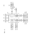
- FIG. 1 is a block diagram showing an image processing system 10 according to some embodiments.
- the image processing system 10 may include an image sensor 100 , an image processor 200 , a display unit 300 , and a lens 500 .
- the image processor 200 may include a camera control unit 210 , an image signal processor 220 , and a PC interface (I/F) 230 .
- the camera control unit 210 may control the control register block 180 .
- the camera control unit 210 may control the image sensor 100 , that is, the control register block 180 by using an inter-integrated circuit (I2C).
- I2C inter-integrated circuit
- the image signal processor 220 may receive image data, which is data output by the buffer 190 , process the image data to generate an image that may be easily viewed by a person, and output the processed the image data to the display unit 300 via the PC I/F 230 .
- FIG. 1 shows that the image signal processor 220 is arranged inside the image processor 200 , the inventive concepts is not limited thereto.
- the image signal processor 220 may be arranged in the image sensor 100 instead.
- the pixel array 110 may include a photosensitive element, such as a photo diode, a photo transistor, a photo gate, or a pinned photo diode (PPD).
- the pixel array 110 may detect a light by using the photosensitive element and transform the light into electric signals, thereby generating video signals.
- the timing generator 170 may control operations or timings of the row driver 120 , the ADC 140 , the ramp signal generator 160 , and the counter controller 171 by outputting control signals or clock signals to the row driver 120 , the ADC 140 , the ramp signal generator 160 , and the counter controller 171
- the control register block 180 may control operations of the timing generator 170 , the counter controller 171 , and the buffer 190 by outputting control signals to the timing generator 170 , the counter controller 171 , and the buffer 190 .
- the control register block 180 may be operated under the control of the camera control unit 210 .
- the counter controller 171 receives a control signal from the control register block 180 , transmits counter control signals (CCS) to a plurality of counters (not shown) included in the ADC 140 , and controls operations of the counters (not shown).
- CCS counter control signals
- the row driver 120 may drive the pixel array 110 row-by-row.
- the row driver 120 may generate a transfer control signal for controlling transfer transistors, a reset control signal for controlling reset transistors, and a select control signal for controlling select transistors of each of unit pixels constituting the pixel array 110 .
- the pixel array 110 outputs a reset signal and a video signal from a row selected based on a row select signal provided by the row driver 120 to the CDS block 130 .
- the CDS block 130 may perform correlated double sampling on the reset signal and the video signal.
- the buffer 190 temporarily stores, senses, and amplifies signals output by the ADC 140 .
- the buffer 190 may include a plurality of column memory blocks (not shown), each of which is included in each column, for temporary storage and a sense amp for sensing and amplifying the digital signals output by the ADC 140 .
- FIG. 2A is a plan view illustrating a portion of a pixel array according to some embodiments.
- a pixel array 110 ′ may be formed on and/or in a substrate may include a device isolation layer 112 and a plurality of unit pixels 114 defined by the device isolation layer 112 .
- the device isolation layer 112 electrically and/or optically isolating adjacent ones of the unit pixels 114 from one another.
- the device isolation layer 112 may be formed, for example, by filling a trench in the substrate formed in a deep trench isolation (DTI) operation with a silicon oxide or a polysilicon.
- DTI deep trench isolation
- the device isolation layer 112 may prevent electric crosstalk that deteriorates a signal-to-noise ratio (SNR) based on carrier exchanges between the unit pixels 114 .
- SNR signal-to-noise ratio
- Sidewalls of the device isolation layer 112 may be doped with a material with a high optical reflection index, thereby preventing optical crosstalk that deteriorates SNR due to transmission of light, which is incident to a particular unit pixel, to another unit pixel adjacent the particular pixel.
- the sidewalls of the device isolation layer 112 may be formed of, for example, a polysilicon doped with boron.
- the inventive concepts are not limited thereto.
- the plurality of unit pixels 114 may form a particular pixel pattern comprising multiple rows along a first direction (x-axis direction) that are offset with respect to one another so that, for example, the unit pixels 114 are arranged in a zig-zag manner along a second direction (y-axis direction) perpendicular to the first direction (x-axis direction).
- the unit pixels 114 are separated from one another by a distance x in the pixel array 110 ′.
- unit pixels 114 b through 114 g may form a honeycomb-like structure in which the unit pixels 114 b through 114 g are radially arranged around a unit pixel 114 a.
- Each of the unit pixels 114 may have various 2-dimensional (2D) shapes.
- the unit pixels 114 may have a regular hexagonal shape with six same-length sides and six identical corner angles ⁇ as illustrated in FIG. 2A .
- the unit pixels 114 may have a non-regular hexagonal shape with different-length sides or different-size corner angles ⁇ .
- the unit pixels 114 may have, for example, other polygonal shapes (e.g., square, rectangular, octagonal, etc.), a circular shape, or an elliptical shape.
- Each of the plurality of unit pixels 114 may include a plurality of transistors, a photoelectric transforming unit, a ground region, and a floating diffusion area. Detailed descriptions thereof are given below with reference to FIGS. 8 and 9 .
- FIG. 2B is a diagram showing a portion A of FIG. 2A in closer detail.
- the device isolation layer 112 between adjacent first through third unit pixels 114 a , 114 b , and 114 c may be Y-shaped.
- a gap area GA 1 may include a corner area CA 1 defined by corners Ca, Cb, and Cc adjacent one another from among corners of the first through third unit pixels 114 a , 114 b , and 114 c.
- An area S 1 of the corner area CA 1 may satisfy Equation 1:
- FIG. 2C is a diagram showing an example of a rectangular pixel array for comparison with the effect of the pixel pattern of FIG. 2A .
- a device isolation layer 112 _ref 1 between first through fourth unit pixels 114 a _ref 1 , 114 b _ref 1 , 114 c _ref 1 , and 114 d _ref 1 may have a cross-like shape as shown in FIG. 2C .
- the area S 1 of the corner area CA 1 of FIG. 2B is smaller than the area S_ref 1 of the corner area CA_ref 1 of FIG. 2C .
- the reduced corner area CA 1 can reduce a risk of stress-based cracks based on a difference between thermal expansion coefficients of a material (e.g., a silicon oxide) constituting the device isolation layer 112 and a material constituting the unit pixels 114 (e.g., polysilicon). Furthermore, the reduced corner area CA 1 can reduce the likelihood of formation of voids in the device isolation layer 112 and, therefore, the likelihood of operational defects due to voids may be reduced.
- a material e.g., a silicon oxide
- FIG. 3A is a diagram showing the portion A of FIG. 2A in closer detail and exemplifies unit pixels 114 ′ with a corner rounding effect.
- the unit pixels 114 ′ with the corner rounding effect may occupy an area smaller than that of the unit pixels 114 of FIG. 2B without the corner rounding effect.
- the corner rounding effect may refer to a phenomenon whereby, while a photo operation or an etching operation for forming unit pixels with polygonal shapes are being performed, corners of the unit pixels with polygonal shapes are rounded. Due to the corner rounding effect, corners Ca′, Cb′, and Cc′ of first through third unit pixels 114 a ′, 114 b ′, and 114 c ′ are rounded, and thus the maximum corner spacing width x+2a′ between the first through third unit pixels 114 a ′, 114 b ′, and 114 c ′ adjacent one another becomes greater than the intended maximum corner spacing distance x (refer to FIG. 2B ).
- the device isolation layer 212 between the adjacent first through third unit pixels 114 a ′, 114 b ′, and 114 c ′ may have rounded Y-shaped gap area GA 1 ′.
- the corner area CA 1 ′ may be defined by the adjacent corners Ca′, Cb′, and Cc′ adjacent one another from among corners of the first through third unit pixels 114 a ′, 114 b ′, and 114 c ′, where an area S 1 ′ of the corner area CA 1 ′ may satisfy Equation 3:
- the maximum corner spacing width ⁇ 2x+2a between the first through fourth unit pixels 114 a _ref 2 , 114 b _ref 2 , 114 c _ref 2 , and 114 d _ref 2 becomes greater than the intended maximum corner spacing width ⁇ 2x (refer to FIG. 2C ).
- a device isolation layer 112 _ref 2 between the first through fourth unit pixels 114 a _ref 2 , 114 b _ref 2 , 114 c _ref 2 , and 114 d _ref 2 may have a rounded cross-like shape as shown in FIG. 3B .
- the gap area GA_ref 2 may include a corner area CA_ref 2 , defined by rounded corners Ca_ref 2 , Cb_ref 2 , Cc_ref 2 , and Cd_ref 2 adjacent one another from among corners of the first through fourth unit pixels 114 a _ref 2 , 114 b _ref 2 , 114 c _ref 2 , and 114 d _ref 2 .
- the area S 1 ′ of the corner area CA 1 ′ of FIG. 3A is greater than the area S 1 of the corner area CA 1 described above with reference to FIG. 2B
- the area S_ref 2 of the corner area CA_ref 2 of FIG. 3B is greater than the area S_ref 1 of the corner area CA_ref 1 described above with reference to FIG. 2C . If unit pixels have a hexagonal shape as shown in FIG. 3A , a corner rounding width increased by the corner rounding effect may become smaller than that in the case where unit pixels have a rectangular shape as shown in FIG. 3B .
- the increased corner rounding width a′ based on Equation 3 may have a smaller value than the increased corner rounding width a based on Equation 4.
- the reason therefor is that corners of a hexagonal shape are less affected by the corner rounding effect than corners of a rectangular shape.
- the area S 1 of the corner area CA 1 may be reduced compared to the case in which unit pixels have a rectangular shape even without the corner rounding effect (refer to FIG. 2B ). Even with the corner rounding effect, a difference between an intended pattern and an actually fabricated pattern may be reduced compared to the case in which unit pixels have a rectangular shape, and thus the area S 1 ′ of the corner area CA 1 ′ formed between unit pixels adjacent one another may be further reduced.
- FIG. 4A is a plan view illustrating a portion of a pixel array according to further embodiments.
- a pixel array 210 ′ formed on and/or in a substrate may include a device isolation layer 212 and a plurality of unit pixels 214 defined by the device isolation layer 212 .
- the device isolation layer 212 may be formed, for example, by filling a trench in the substrate formed in a DTI operation with a silicon oxide or a polysilicon.
- sidewalls of the device isolation layer 212 may be doped with a material with a high optical reflection index, thereby reducing optical crosstalk.
- the unit pixels 214 may have a square shape with a same length L 2 on all four sides and the same corner angles ⁇ 2 . In some embodiments, the unit pixels 214 may have a rectangular shape with different side lengths L 2 .
- the plurality of unit pixels 214 may form a particular pixel pattern and be separated apart from one another at the distance x in the pixel array 210 ′.
- unit pixels 214 b through 214 g may form a honeycomb-like structure in which the unit pixels 214 b through 214 g are radially arranged around a unit pixel 214 a.
- the unit pixels 214 may be linearly arranged along a first direction (x-axis direction) and may be arranged in a zig-zag manner along a second direction (y-axis direction) perpendicular to the first direction (x-axis direction).
- the device isolation layer 212 between first through third unit pixels 214 a , 214 b , and 214 c adjacent one another may have a T-like shape. If the gap area GA 2 has a T-like shape, increase of a corner area due to the corner rounding effect may be reduced, thereby reducing stress-based cracks and a void.
- FIG. 4B is a diagram showing a portion B of FIG. 4A in closer detail and exemplifies unit pixels 214 ′ with the corner rounding effect.
- the unit pixels 214 ′ with the corner rounding effect may occupy an area smaller than that of the unit pixels 214 without the corner rounding effect.
- the maximum corner spacing width ⁇ x2+a′′ between unit pixels 214 a ′, 214 c ′, and 214 d ′ adjacent one another becomes greater than the intended maximum corner spacing width ⁇ 2x (see FIG. 2C ).
- the gap area GA 2 (refer to FIG. 4A ) has a T-like shape
- increase of a corner area due to the corner rounding effect may be reduced.
- the area S_ref 2 of the corner area CA_ref 2 is affected by the corner rounding effect at the four corners Ca_ref 2 , Cb_ref 2 , Cc_ref 2 , and Cd_ref 2 (refer to FIG. 3B ).
- the area S 2 ′ of the corner area CA 2 ′ is only affected by the corner rounding effect at the two corners Ca 2 ′ and Cd 2 ′.
- FIG. 5A is a plan view illustrating a pixel array according to another exemplary embodiment.
- a pixel array 310 ′ on and/or in a substrate may include a device isolation layer 312 and a plurality of unit pixels 314 defined by the device isolation layer 312 .
- Each of unit pixels 314 of FIG. 5A has a structure similar to that of the unit pixels 214 described above with reference to FIG. 4A , but each of the unit pixels 314 includes a protrusion 316 unlike the unit pixels 214 . Detailed descriptions of components other than the protrusion 316 will be omitted for simplification of explanation.
- the protrusion 316 extending in a first direction (x-axis direction) is formed at at least one side sc of each of the plurality of unit pixels 314 .
- the protrusions 316 are formed at two opposite sides sc of each of the unit pixels 314 extending in the first direction (x-axis direction).
- the protrusions 316 may be formed at only one of the sides sc extending in the first direction (x-axis direction).
- the protrusion 316 may be formed at the center of the side sc and reduce an area of the corner area CA 3 ′ (see FIG. 5B ).
- the protrusion 316 has a triangular shape in the illustrated embodiments, the inventive concepts are not limited thereto, and the protrusion 316 may have any of various shapes.
- FIG. 5B is a diagram showing an area C of FIG. 5A in closer detail and exemplifies unit pixels 314 ′ with the corner rounding effect.
- an area S 3 ′ of the corner area CA 3 ′ may be reduced by the area of the protrusion 316 .
- FIG. 6A is a plan view illustrating a portion of a pixel array according to another exemplary embodiment.
- FIG. 6B is a diagram showing a portion D of FIG. 6A in closer detail.
- a pixel array 410 ′ formed on and/or in a substrate may include a device isolation layer 412 and a plurality of unit pixels 414 defined by the device isolation layer 412 .
- the device isolation layer 412 may be formed, for example, by filling a trench formed in a DTI operation with a silicon oxide or a polysilicon, for example.
- sidewalls of the device isolation layer 412 may be doped with a material with a high optical reflection index, thereby reducing optical crosstalk.
- the unit pixel 414 may have a circular shape in a plan view image. According to some embodiments, the unit pixel 414 may have an elliptical shape. If the unit pixels 414 have a circular shape or an elliptical shape as in the present exemplary embodiment, the unit pixels 414 do not have rounded corners, and thus the corner rounding effect may be reduced or suppressed, and thus a difference between an intended pattern and an actually fabricated pattern that may occur during a photo operation or an etching operation may be reduced.
- Unit pixels 414 b through 414 g may form a honeycomb-like structure, in which the unit pixels 414 b through 414 g are separated apart from one another by the distance x and are radially arranged around a unit pixel 414 a .
- the unit pixels 414 may be linearly arranged along a first direction (x-axis direction) and may be arranged in a zig-zag manner in a second direction (y-axis direction) perpendicular to the first direction (x-axis direction).
- an area S 4 of a corner area CA 4 may be reduced without the corner rounding effect.
- Equation 9 a relationship among the area S 4 of the corner area CA 4 , the distance x, and the radius r of each of the unit pixels 414 may be as shown in Equation 9:
- the area S 4 of the corner area CA 4 may be reduced by adjusting the radius r of each of the unit pixels 414 .
- the radius r of each of the unit pixels 414 is adjusted within the range defined by Equation 10 above, the area S 4 of the corner area CA 4 becomes smaller than the area S 1 _ref 1 of the corner area CA_ref 1 described above with reference to FIG. 2C .
- FIGS. 7A through 7C are circuit diagrams of unit pixels according to some embodiments.
- a unit pixel 114 _ 1 may include a photo diode PD, a transfer transistor Tx, a floating diffusion node FD, a reset transistor Rx, a driver transistor Dx, and a select transistor Sx.
- the photo diode PD is an example of a photoelectric transforming unit that may be used, and may include a photo diode, a photo gate, a pinned photo diode, or a combination thereof.
- FIG. 7A shows a unit pixel with a 4-transistor (4T) structure including one photo diode PD and four MOS transistors Tx, Rx, Dx, and Sx.
- 4T 4-transistor
- a unit pixel may include any of various numbers of transistors.
- the photo diode PD may generate photo charges that vary according to intensity of a light incident from a target object.
- the transfer transistor Tx may transfer the generated photo charges to the floating diffusion node FD based on a transfer control signal TG output by the row driver 120 .
- the driver transistor Dx may amplify a potential at the floating diffusion node and transfer the photo charges to the select transistor Sx.
- a drain terminal of the select transistor Sx is connected to a source terminal of the driver transistor Dx, and the select transistor Sx may output a pixel signal to a column line connected to the unit pixel 114 _ 1 according to a selecting signal SEL output by the row driver 120 .
- the reset transistor Rx may reset the floating diffusion node FD to VDD responsive to a reset control signal RS output by the row driver 120 .
- a unit pixel 114 _ 2 may have a 3-transistor (3T) structure and may include a photo diode PD, a reset transistor Rx, a driver transistor Dx, and a select transistor Sx. Photo charges generated by the photo diode PD may be immediately accumulated at the floating diffusion node FD and pixel signals may be output to column lines based on operations of the driver transistor Dx and the select transistor Sx.
- 3T 3-transistor
- a unit pixel 114 _ 3 may have a 3T structure and may include a photo diode PD, a transfer transistor Tx, a reset transistor Rx, and a driver transistor Dx.
- the reset transistor Rx may be embodied as an n-channel depression type transistor.
- the reset transistor Rx may perform a function similar to that of the select transistor Sx by resetting the floating diffusion node FD or setting the floating diffusion node FD to a low level (e.g., 0V) responsive to a reset control signal output by the row driver 120 .
- FIG. 8 is a plan view illustrating a structure of a unit pixel according to some embodiments.
- a pixel array of an image sensor may include a first device isolation layer 11 and a plurality of unit pixels PX defined by the first device isolation layer 11 .
- Each of the unit pixels PX may include a photoelectric transforming unit PD formed in and/or on a semiconductor substrate, a second device isolation layer 12 that defines active areas 20 , 30 , and 50 , and a plurality of transistors Tx, Rx, Dx, and Sx formed at the active areas 20 , 30 , and 50 .
- the photoelectric transforming unit PD may be a region formed inside the semiconductor substrate and may have a first conductivity type.
- the first conductivity type may be n type, for example, the photoelectric transforming unit PD may be an n type semiconductor region doped with an n type impurity.
- the semiconductor substrate may comprise a p-type material and the n type photoelectric transforming unit PD may form a PN junction with the p-type semiconductor material of the substrate and form a photo diode.
- the photoelectric transforming unit PD may receive an incident light and generate and accumulate charges.
- the photoelectric transforming unit PD may be formed apart from sidewalls of the first device isolation layer 11 .
- the second device isolation layer 12 defining the active areas 20 , 30 , and 50 may be formed at each of the unit pixels PX.
- the second device isolation layer 12 may be formed inside the first device isolation layer 11 and may contact the first device isolation layer 11 .
- the second device isolation layer 12 may be formed of a same insulation material as the first device isolation layer 11 .
- the second device isolation layer 12 may be, for example, a trench-type device isolation layer and may be formed in a shallow trench isolation (STI) operation.
- the active areas 20 , 30 , and 50 may include a first active area 20 , a second active area 30 , and a third active area 50 that are isolated from one another by the second device isolation layer 12 .
- a floating diffusion region 21 and a transfer gate TG of the transfer transistor Tx may be formed at the first active area 20 .
- a ground region 31 may be formed at the second active area 30 .
- the floating diffusion region 21 may have the first conductivity type.
- the floating diffusion region 21 may be an N+ type semiconductor region doped with an N+ type impurity.
- the floating diffusion region 21 may correspond to the floating diffusion node FD shown in FIG. 7A .
- the ground region 31 may have a second conductivity type.
- the ground region 31 may be a P+ type semiconductor region doped with a P+ type impurity.
- the transfer gate TG may be formed of polysilicon.
- the transfer transistor Tx of FIG. 7A may include the photoelectric transforming unit PD, the floating diffusion region 21 , and the transfer gate TG.
- Charges generated by the photoelectric transforming unit PD may be transferred to the floating diffusion region 21 via a channel (not shown) formed below the transfer gate TG.
- the third active area 50 may extend in a L-clamp-like shape along a first side side 1 and a second side side 2 from among sides of the hexagonal unit pixel PX that are adjacent the third active area 50 .
- the shape of the third active area 50 is not limited thereto, and various modifications may be made therein according to shape of the unit pixel PX.
- the floating diffusion region 21 may be electrically connected to the first semiconductor region 51 , which is the source of the reset transistor Rx, via a first contact 41 and a third contact 43 .
- the floating diffusion region 21 may be electrically connected to the drive gate DG of the driver transistor Dx via the first contact 41 , the third contact 43 , and a fifth contact 45 .
- the ground region 31 may be electrically connected to a ground voltage terminal GND via a second contact 42 .
- the second semiconductor region 52 which is a drain of the reset transistor Rx and the driver transistor Dx, may be electrically connected to a power supply terminal VDD via a fourth contact 44 .
- the fourth semiconductor region 54 which is a source of the select transistor Sx, may be electrically connected to an output terminal OUT via a sixth contact 46 .
- each of the unit pixels PX includes all of the transistors Rx, Dx, and Sx in the illustrated embodiments, the inventive concepts are not limited thereto.
- the unit pixel PX may have a structure in which at least one of the transistors Rx, Dx, and Sx is omitted or a structure in which at least one transistor is shared as shown in FIG. 9A and FIG. 9B .
- FIG. 9A is a block diagram illustrating a layout of two adjacent unit pixels Px_ 1 and Px_ 2 using shared transistors according to some embodiments.
- the first unit pixel Px_ 1 and the second unit pixel Px_ 2 may be electrically isolated from each other by the first device isolation layer 11 , and internal components of each of the first unit pixel Px_ 1 and the second unit pixel Px_ 2 may be electrically isolated from one another by second device isolation layers 12 _ 1 and 12 _ 2 .
- the first unit pixel Px_ 1 and the second unit pixel Px_ 2 include floating diffusion areas 21 _ 1 and 21 _ 2 , ground regions 31 _ 1 and 31 _ 2 , respectively.
- the first unit pixel Px_ 1 and the second unit pixel Px_ 2 include a first transfer transistor Tx_ 1 and a second transfer transistor Tx_ 2 , respectively.
- the respective floating diffusion areas 21 _ 1 and 21 _ 2 of the first unit pixel Px_ 1 and the second unit pixel Px_ 2 may be connected to each other via a conductive line (not shown) and function as a single node.
- the first unit pixel Px_ 1 and the second unit pixel Px_ 2 may include a first supplemental transistor Sux_ 1 and a second supplemental transistor Sux_ 2 , respectively.
- the first supplemental transistor Sux_ 1 may function like the reset transistor Rx described above with respect to FIG. 8
- the second supplemental transistor Sux_ 2 may function like the driver transistor Dx described above with respect to FIG. 8 .
- the first unit pixel Px_ 1 and the second unit pixel Px_ 2 may share the floating diffusion areas 21 _ 1 and 21 _ 2 , the reset transistor Rx, and the driver transistor Dx, and thus each of the first unit pixel Px_ 1 and the second unit pixel Px_ 2 may include only two transistors. Therefore, an area occupied by each pixel in the first unit pixel Px_ 1 and the second unit pixel Px_ 2 may be minimized.
- FIG. 9B is a block diagram illustrating a layout of two adjacent unit pixels Px_ 1 and Px_ 2 using shared transistors according to some embodiments.
- the first unit pixel Px_ 1 and the second unit pixel Px_ 2 may be electrically isolated from each other by the first device isolation layer 11 , and internal components of each of the first unit pixel Px_ 1 and the second unit pixel Px_ 2 may be electrically isolated from one another by second device isolation layers 12 _ 1 and 12 _ 2 .
- the first unit pixel Px_ 1 and the second unit pixel Px_ 2 include floating diffusion areas 21 _ 1 and 21 _ 2 , ground regions 31 _ 1 and 31 _ 2 , respectively.
- the first unit pixel Px_ 1 and the second unit pixel Px_ 2 include a first transfer transistor Tx_ 1 and a second transfer transistor Tx_ 2 , respectively.
- the respective floating diffusion areas 21 _ 1 and 21 _ 2 of the first unit pixel Px_ 1 and the second unit pixel Px_ 2 may be connected to each other via a conductive line (not shown) and function as a single node.
- the first unit pixel Px_ 1 may include a first supplemental transistor Sux_ 1 and a third supplemental transistor Sux_ 3
- the second unit pixel Px_ 2 may include a second supplemental transistor Sux_ 2 , respectively.
- the first supplemental transistor Sux_ 1 may function like the reset transistor Rx described above with respect to FIG. 8
- the third supplemental transistor Sux_ 3 may function like the select transistor Sx described above with respect to FIG. 8
- the second supplemental transistor Sux_ 2 may function like the driver transistor Dx described above with respect to FIG. 8 .
- FIG. 9A and FIG. 9B show that the first unit pixel Px_ 1 and the second unit pixel Px_ 2 are arranged in a vertical direction, the first unit pixel Px_ 1 and the second unit pixel Px_ 2 may have other arrangements.
- a plurality of first unit pixels Px_ 1 and a plurality of second unit pixels Px_ 2 may be repeatedly arranged to form a pixel array, such as those described above with reference to FIGS. 1 through 6B .
- FIGS. 10A through 10C are diagrams illustrating color filter arrangements applicable to pixel arrays according to some embodiments.
- a pixel group PU_a including three adjacent unit pixels Px_a, Px_b, and Px_c may be included in a pixel array PA_a.
- Various color filters (not shown) may be arranged at each of the unit pixels Px_a, Px_b, and Px_c included in the pixel group PU_a.
- the color filters may selectively transmit lights of wavelengths corresponding to particular colors (e.g., red, green, blue, magenta, yellow, cyan, etc.)
- a red filter R may be arranged at a first unit pixel PX_a
- a green filter G may be arranged at a second unit pixel PX_b
- a blue filter B may be arranged at a third unit pixel PX_c.
- the pixel groups PU_b and PU_c each of which consists of four unit pixels adjacent one another, may be included in pixel arrays PA_b and PA_c, respectively.
- each of the pixel groups PU_b and PU_c may include four unit pixels adjacent one another.
- Various color filters may be arranged at each of unit pixels of the pixel groups PU_b and PU_c. For example, as shown in FIG.
- the green filter G may be arranged at the first and second unit pixels Px_a and Px_b included in the pixel group PU_b, the blue filter B may be arranged at the third unit pixel PX_c, and the red filter R may be arranged at the fourth unit pixel PX_d.
- the green filter G may be arranged at the first and fifth unit pixels Px_a and Px_e included in the pixel group PU_b, the red filter R may be arranged at the second unit pixel PX_b, and the blue filter B may be arranged at the third unit pixel PX_c.
- FIG. 11 is a diagram illustrating an electronic system 1000 including an image sensor having a pixel pattern according to some embodiments.
- the electronic system 1000 may be embodied as a data processing device that is capable of using or supports a mobile industry processor interface (MIPI), e.g., a mobile phone, a PDA, a PMP, an IPTV, or a smart phone.
- MIPI mobile industry processor interface
- the electronic system 1000 may include an application processor 1010 , an image sensor 1040 , and a display 1050 .
- a CSI host 1012 embodied at the application processor 1010 may serial communicate with a CSI device 1041 of the image sensor 1040 via a camera serial interface (CSI).
- An optical de-serializer may be embodied at the CSI host 1012
- an optical serializer may be embodied at the CSI device 1041 .
- a DSI host 1011 embodied at the application processor 1010 may serial communicate with a DSI device 1051 of the display 1050 via a display serial interface (DSI).
- DSI display serial interface
- An optical serializer may be embodied at the DSI host 1011
- an optical de-serializer may be embodied at the DSI device 1051 .
- the image sensor 1040 may include a pixel array having a pixel pattern according to one of the embodiments described above with reference to FIGS. 1 through 10C .
- the electronic system 1000 may further include a RF chip 1060 capable of communicating with the application processor 1010 .
- a PHY 1013 of the electronic system 1000 and a PHY 1061 of the RF chip 1060 may exchange data according to MIPI DigRF.
- the electronic system 1000 may further include a GPS 1020 , a storage 1070 , a microphone 1080 , a DRAM 1085 , and a speaker 1090 , where the electronic system 1000 may communicate by using a Wimax 1030 , a WLAN 1100 , and a UWB 1110 .
- FIG. 12 is a block diagram showing an image processing system 1100 including an image sensor having a pixel pattern according to some embodiments.
- the image processing system 1100 may include a processor 1110 , a memory 1120 , the image sensor 100 , a display unit 1130 , and an interface 1140 .
- the processor 1110 may control operations of the image sensor 100 .
- the processor 1110 may generate a 2D image or a 3D image based on depth information and color information (e.g., at least one of red information, green information, blue information, magenta information, cyan information, and yellow information) from the image sensor 100 .
- color information e.g., at least one of red information, green information, blue information, magenta information, cyan information, and yellow information
- the memory 1120 may store a program for controlling operations of the image sensor 100 via the bus 1150 and the generated image under the control of the processor 1110 , and the processor 1110 may execute the program by accessing data stored in the memory 1120 .
- the memory 1120 may be embodied as a non-volatile memory, for example.
- the image sensor 100 may generate 2D or 3D image information based on respective digital pixel signals (e.g., color information or depth information) under the control of the processor 1110 .
- respective digital pixel signals e.g., color information or depth information
- the image sensor 100 may include a pixel array having a pixel pattern according to some embodiments described above with reference to FIGS. 1 through 10C .
- the display unit 1130 may receive the generated image from the processor 1110 or the memory 1120 and display via a display element (e.g., an LCD, an AMOLED, etc.).
- a display element e.g., an LCD, an AMOLED, etc.
- the interface 1140 may be embodied as an interface for inputting and outputting 2D images or 3D images. According to some embodiments, the interface 1140 may be embodied as a wireless interface.
- FIGS. 13 through 17 are diagrams showing examples of multimedia devices employing image sensors according to some embodiments.
- Image sensors including pixel patterns may be applied to various multimedia devices with image pickup function.
- an image sensor may be applied to a mobile phone or smart phone 3000 as shown in FIG. 13 or may be applied to a tablet or smart tablet 4000 as shown in FIG. 14 .
- an image sensor according to some embodiments may be applied to a laptop computer 5000 as shown in FIG. 15 or may be applied to a smart TV 6000 as shown in FIG. 16 .
- An image sensor according to some embodiments may also be applied to a digital camera or digital camcorder 7000 .
Abstract
Description
S<x 2.
In further embodiments, each of the first, second and third unit pixels has a rounded hexagonal shape and the portion of the DTI layer bounded by the segments connecting the adjacent corners of the first, second and third unit pixels has an area S given by:
wherein a′ denotes a corner rounding width. The distance x may be from about 100 nm to about 300 nm.
S=½(√{square root over (2)}x+a′)2,
wherein a″ denotes a corner rounding width.
S=½(√{square root over (2)}x+a″)2 −Sp,
wherein a″ denotes a corner rounding width and Sp denotes an area of the protrusion.
wherein r denotes a radius of the first, second and third unit pixels. The distance x and the radius r satisfy the following:
r≦1.939x.
S_ref1=x 2. (2)
where a′ denotes a corner rounding width increased at the corners Ca′, Cb′, and Cc′ due to the corner rounding effect.
S_ref2=½(√{square root over (2)}x+2a)2, (4)
where a denotes a corner rounding width increased at the corners Ca_ref2, Cb_ref2, Cc_ref2, and Cd_ref2 due to the corner rounding effect.
S2′=½(√{square root over (2)}x+a″)2, (5)
where a″ denotes a corner rounding width increased at the corners Ca2′ and Cb2′ due to the corner rounding effect.
S3′=½(√{square root over (2)}x+a″)2 −Sp, (6)
where a″ denotes a corner rounding width increased at the corners Ca2′ and Cb2′ due to the corner rounding effect and Sp denotes an area of the
where re denotes a length of a side of the regular triangle.
re=(x+(2−√3)*r)2. (8)
r≦1.939x. (10)
Claims (9)
S<x 2.
r≦1.939x.
Applications Claiming Priority (2)
| Application Number | Priority Date | Filing Date | Title |
|---|---|---|---|
| KR1020150034040A KR102242563B1 (en) | 2015-03-11 | 2015-03-11 | Pixel pattern and image sensor comprising the same |
| KR10-2015-0034040 | 2015-03-11 |
Publications (2)
| Publication Number | Publication Date |
|---|---|
| US20160268321A1 US20160268321A1 (en) | 2016-09-15 |
| US9793310B2 true US9793310B2 (en) | 2017-10-17 |
Family
ID=56888206
Family Applications (1)
| Application Number | Title | Priority Date | Filing Date |
|---|---|---|---|
| US15/065,962 Expired - Fee Related US9793310B2 (en) | 2015-03-11 | 2016-03-10 | Image sensor devices using offset pixel patterns |
Country Status (2)
| Country | Link |
|---|---|
| US (1) | US9793310B2 (en) |
| KR (1) | KR102242563B1 (en) |
Cited By (1)
| Publication number | Priority date | Publication date | Assignee | Title |
|---|---|---|---|---|
| US11018173B2 (en) | 2018-06-18 | 2021-05-25 | Samsung Electronics Co., Ltd. | Image sensor |
Families Citing this family (3)
| Publication number | Priority date | Publication date | Assignee | Title |
|---|---|---|---|---|
| KR102622057B1 (en) | 2016-12-29 | 2024-01-05 | 삼성전자주식회사 | Image sensor |
| KR20200036137A (en) * | 2018-09-27 | 2020-04-07 | 삼성디스플레이 주식회사 | Display device |
| TW202226564A (en) * | 2020-12-25 | 2022-07-01 | 日商索尼半導體解決方案公司 | Solid-state imaging device and method for manufacturing same |
Citations (21)
| Publication number | Priority date | Publication date | Assignee | Title |
|---|---|---|---|---|
| US20030151075A1 (en) | 2002-02-14 | 2003-08-14 | Makoto Shizukuishi | Solid-state image pick-up device |
| US20050104989A1 (en) * | 2003-11-14 | 2005-05-19 | Fuji Photo Film Co., Ltd. | Dual-type solid state color image pickup apparatus and digital camera |
| US20060118837A1 (en) | 2004-12-07 | 2006-06-08 | Sung-Ho Choi | Active pixel sensor having honeycomb structure |
| US20070018073A1 (en) | 2005-07-22 | 2007-01-25 | Taiwan Semiconductor Manufacturing Co., Ltd. | CMOS image sensor device with beehive pattern color sensor cell array |
| JP2007288294A (en) | 2006-04-13 | 2007-11-01 | Matsushita Electric Ind Co Ltd | Solid-state imaging apparatus and camera |
| US20080018765A1 (en) | 2006-07-19 | 2008-01-24 | Samsung Electronics Company, Ltd. | CMOS image sensor and image sensing method using the same |
| KR20090037604A (en) | 2007-10-12 | 2009-04-16 | 주식회사 동부하이텍 | Vertical-type cmos image sensor and method for fabricating thereof |
| JP2009158689A (en) | 2007-12-26 | 2009-07-16 | Fujifilm Corp | Solid-state imaging element |
| US7612812B2 (en) | 2004-02-16 | 2009-11-03 | Fujifilm Corporation | Solid state imaging device with increased vertical resolution in interlace scanning method |
| US20100171854A1 (en) | 2009-01-08 | 2010-07-08 | Sony Corporation | Solid-state imaging device |
| JP2010153603A (en) | 2008-12-25 | 2010-07-08 | Fujifilm Corp | Solid state imaging apparatus |
| US7821090B2 (en) | 2007-04-03 | 2010-10-26 | Sharp Kabushiki Kaisha | Solid-state image capturing apparatus, method for manufacturing the same, and electronic information device |
| US7872287B2 (en) | 2007-09-12 | 2011-01-18 | Unisantis Electronics (Japan) Ltd. | Solid-state imaging device |
| US20120268566A1 (en) | 2011-04-21 | 2012-10-25 | Samsung Electronics Co., Ltd. | Three-dimensional color image sensors having spaced-apart multi-pixel color regions therein |
| US20130127002A1 (en) | 2010-07-12 | 2013-05-23 | Fujifilm Corporation | Solid state imaging device |
| US20130153748A1 (en) | 2011-12-14 | 2013-06-20 | Sony Corporation | Solid-state image sensor and electronic apparatus |
| US8569855B2 (en) | 2009-05-19 | 2013-10-29 | Sony Corporation | Two-dimensional solid-state imaging device |
| KR20140029933A (en) | 2012-08-31 | 2014-03-11 | 에스케이하이닉스 주식회사 | Lensless image sensore |
| US8822897B2 (en) | 2010-03-19 | 2014-09-02 | Invisage Technologies, Inc. | Image sensors employing sensitized semiconductor diodes |
| US20150015768A1 (en) * | 2012-03-30 | 2015-01-15 | Fujifilm Corporation | Imaging element and imaging device |
| US9432113B2 (en) * | 2012-06-11 | 2016-08-30 | Fujitsu Limited | Optical transmission device |
Family Cites Families (2)
| Publication number | Priority date | Publication date | Assignee | Title |
|---|---|---|---|---|
| JP2008136145A (en) * | 2006-11-29 | 2008-06-12 | Kyocera Corp | Imaging device, and manufacturing device and manufacturing method thereof |
| KR102034482B1 (en) * | 2013-03-04 | 2019-10-21 | 삼성전자주식회사 | Image sensor and method of forming the same |
-
2015
- 2015-03-11 KR KR1020150034040A patent/KR102242563B1/en active IP Right Grant
-
2016
- 2016-03-10 US US15/065,962 patent/US9793310B2/en not_active Expired - Fee Related
Patent Citations (22)
| Publication number | Priority date | Publication date | Assignee | Title |
|---|---|---|---|---|
| US20030151075A1 (en) | 2002-02-14 | 2003-08-14 | Makoto Shizukuishi | Solid-state image pick-up device |
| US20050104989A1 (en) * | 2003-11-14 | 2005-05-19 | Fuji Photo Film Co., Ltd. | Dual-type solid state color image pickup apparatus and digital camera |
| US7612812B2 (en) | 2004-02-16 | 2009-11-03 | Fujifilm Corporation | Solid state imaging device with increased vertical resolution in interlace scanning method |
| US20060118837A1 (en) | 2004-12-07 | 2006-06-08 | Sung-Ho Choi | Active pixel sensor having honeycomb structure |
| US20070018073A1 (en) | 2005-07-22 | 2007-01-25 | Taiwan Semiconductor Manufacturing Co., Ltd. | CMOS image sensor device with beehive pattern color sensor cell array |
| JP2007288294A (en) | 2006-04-13 | 2007-11-01 | Matsushita Electric Ind Co Ltd | Solid-state imaging apparatus and camera |
| US7825970B2 (en) | 2006-07-19 | 2010-11-02 | Samsung Electronics Co., Ltd. | CMOS image sensor and image sensing method using the same |
| US20080018765A1 (en) | 2006-07-19 | 2008-01-24 | Samsung Electronics Company, Ltd. | CMOS image sensor and image sensing method using the same |
| US7821090B2 (en) | 2007-04-03 | 2010-10-26 | Sharp Kabushiki Kaisha | Solid-state image capturing apparatus, method for manufacturing the same, and electronic information device |
| US7872287B2 (en) | 2007-09-12 | 2011-01-18 | Unisantis Electronics (Japan) Ltd. | Solid-state imaging device |
| KR20090037604A (en) | 2007-10-12 | 2009-04-16 | 주식회사 동부하이텍 | Vertical-type cmos image sensor and method for fabricating thereof |
| JP2009158689A (en) | 2007-12-26 | 2009-07-16 | Fujifilm Corp | Solid-state imaging element |
| JP2010153603A (en) | 2008-12-25 | 2010-07-08 | Fujifilm Corp | Solid state imaging apparatus |
| US20100171854A1 (en) | 2009-01-08 | 2010-07-08 | Sony Corporation | Solid-state imaging device |
| US8569855B2 (en) | 2009-05-19 | 2013-10-29 | Sony Corporation | Two-dimensional solid-state imaging device |
| US8822897B2 (en) | 2010-03-19 | 2014-09-02 | Invisage Technologies, Inc. | Image sensors employing sensitized semiconductor diodes |
| US20130127002A1 (en) | 2010-07-12 | 2013-05-23 | Fujifilm Corporation | Solid state imaging device |
| US20120268566A1 (en) | 2011-04-21 | 2012-10-25 | Samsung Electronics Co., Ltd. | Three-dimensional color image sensors having spaced-apart multi-pixel color regions therein |
| US20130153748A1 (en) | 2011-12-14 | 2013-06-20 | Sony Corporation | Solid-state image sensor and electronic apparatus |
| US20150015768A1 (en) * | 2012-03-30 | 2015-01-15 | Fujifilm Corporation | Imaging element and imaging device |
| US9432113B2 (en) * | 2012-06-11 | 2016-08-30 | Fujitsu Limited | Optical transmission device |
| KR20140029933A (en) | 2012-08-31 | 2014-03-11 | 에스케이하이닉스 주식회사 | Lensless image sensore |
Non-Patent Citations (1)
| Title |
|---|
| Yamada et al. "MP 6.5 A Progressive Scan CCD Imager for DSC Applications" 2000 IEEE International Solid-State Circuits Conference, 2 Pages. |
Cited By (1)
| Publication number | Priority date | Publication date | Assignee | Title |
|---|---|---|---|---|
| US11018173B2 (en) | 2018-06-18 | 2021-05-25 | Samsung Electronics Co., Ltd. | Image sensor |
Also Published As
| Publication number | Publication date |
|---|---|
| KR20160109514A (en) | 2016-09-21 |
| US20160268321A1 (en) | 2016-09-15 |
| KR102242563B1 (en) | 2021-04-20 |
Similar Documents
| Publication | Publication Date | Title |
|---|---|---|
| US9025063B2 (en) | Unit pixel of image sensor and pixel array including the unit pixel | |
| US9954034B2 (en) | Image sensor, method for manufacturing the same, and image processing device having the image sensor | |
| US9966407B2 (en) | Unit pixels, image sensors including the same, and image processing systems including the same | |
| US9887217B2 (en) | Pixels of image sensors, image sensors including the pixels, and image processing systems including the image sensors | |
| US9609250B2 (en) | Unit pixels for image sensors and pixel arrays comprising the same | |
| US9997556B2 (en) | Image sensor | |
| US10447976B2 (en) | Solid state imaging device having a shared pixel structure and electronic apparatus | |
| US9420209B2 (en) | Method of generating pixel array layout for image sensor and layout generating system using the method | |
| US10432831B2 (en) | Image sensor | |
| US9793310B2 (en) | Image sensor devices using offset pixel patterns | |
| US10313616B2 (en) | Image sensors including shielding structures | |
| KR20160005573A (en) | Image sensor, image processing system including the same, and mobile electronic device including the same | |
| KR102465576B1 (en) | Image sensor and method for fabricating the same | |
| JP2016021479A (en) | Solid-state image sensor, manufacturing method and electronic apparatus | |
| US9960201B2 (en) | Image sensor and pixel of the image sensor | |
| US11670660B2 (en) | Pixel array included in auto-focus image sensor and auto-focus image sensor including the same | |
| US8853606B2 (en) | Image sensor cell, image sensor including image sensor array including plurality of the image sensor cells, and camera system including the image sensor | |
| US10446599B2 (en) | Image sensor with phase difference detection pixel | |
| US20210358980A1 (en) | Image sensing device | |
| US20230032117A1 (en) | Image sensing device |
Legal Events
| Date | Code | Title | Description |
|---|---|---|---|
| AS | Assignment |
Owner name: SAMSUNG ELECTRONICS CO., LTD., KOREA, REPUBLIC OF Free format text: ASSIGNMENT OF ASSIGNORS INTEREST;ASSIGNORS:IHARA, HISANORI;YANG, JUN-SEOK;REEL/FRAME:037947/0316 Effective date: 20151030 |
|
| AS | Assignment |
Owner name: SAMSUNG ELECTRONICS CO., LTD., KOREA, REPUBLIC OF Free format text: ASSIGNMENT OF ASSIGNORS INTEREST;ASSIGNOR:JUNG, SANG-IL;REEL/FRAME:039068/0331 Effective date: 20151030 |
|
| STCF | Information on status: patent grant |
Free format text: PATENTED CASE |
|
| FEPP | Fee payment procedure |
Free format text: MAINTENANCE FEE REMINDER MAILED (ORIGINAL EVENT CODE: REM.); ENTITY STATUS OF PATENT OWNER: LARGE ENTITY |
|
| LAPS | Lapse for failure to pay maintenance fees |
Free format text: PATENT EXPIRED FOR FAILURE TO PAY MAINTENANCE FEES (ORIGINAL EVENT CODE: EXP.); ENTITY STATUS OF PATENT OWNER: LARGE ENTITY |
|
| STCH | Information on status: patent discontinuation |
Free format text: PATENT EXPIRED DUE TO NONPAYMENT OF MAINTENANCE FEES UNDER 37 CFR 1.362 |
|
| FP | Lapsed due to failure to pay maintenance fee |
Effective date: 20211017 |