US9793088B2 - Two-stage dodecapole aberration corrector for charged-particle beam - Google Patents
Two-stage dodecapole aberration corrector for charged-particle beam Download PDFInfo
- Publication number
- US9793088B2 US9793088B2 US12/564,277 US56427709A US9793088B2 US 9793088 B2 US9793088 B2 US 9793088B2 US 56427709 A US56427709 A US 56427709A US 9793088 B2 US9793088 B2 US 9793088B2
- Authority
- US
- United States
- Prior art keywords
- poles
- dodecapole
- optical axis
- elements
- polarity
- Prior art date
- Legal status (The legal status is an assumption and is not a legal conclusion. Google has not performed a legal analysis and makes no representation as to the accuracy of the status listed.)
- Active, expires
Links
- 230000004075 alteration Effects 0.000 title claims abstract description 81
- 239000002245 particle Substances 0.000 title claims description 18
- 230000002441 reversible effect Effects 0.000 claims abstract 11
- 230000005684 electric field Effects 0.000 claims description 50
- 230000005405 multipole Effects 0.000 claims description 27
- 230000003287 optical effect Effects 0.000 abstract description 80
- 201000009310 astigmatism Diseases 0.000 description 36
- 238000010894 electron beam technology Methods 0.000 description 22
- 238000012546 transfer Methods 0.000 description 15
- 238000010586 diagram Methods 0.000 description 9
- 239000000523 sample Substances 0.000 description 9
- 230000005540 biological transmission Effects 0.000 description 7
- 238000012937 correction Methods 0.000 description 5
- 238000005286 illumination Methods 0.000 description 5
- 230000003068 static effect Effects 0.000 description 4
- 238000000034 method Methods 0.000 description 3
- 238000004804 winding Methods 0.000 description 2
- 206010010071 Coma Diseases 0.000 description 1
- 206010073261 Ovarian theca cell tumour Diseases 0.000 description 1
- 230000001419 dependent effect Effects 0.000 description 1
- 238000013461 design Methods 0.000 description 1
- 238000009826 distribution Methods 0.000 description 1
- 230000000694 effects Effects 0.000 description 1
- 229940029329 intrinsic factor Drugs 0.000 description 1
- 238000010884 ion-beam technique Methods 0.000 description 1
- 238000003754 machining Methods 0.000 description 1
- 238000012986 modification Methods 0.000 description 1
- 230000004048 modification Effects 0.000 description 1
- 208000001644 thecoma Diseases 0.000 description 1
Images


Classifications
-
- H—ELECTRICITY
- H01—ELECTRIC ELEMENTS
- H01J—ELECTRIC DISCHARGE TUBES OR DISCHARGE LAMPS
- H01J37/00—Discharge tubes with provision for introducing objects or material to be exposed to the discharge, e.g. for the purpose of examination or processing thereof
- H01J37/02—Details
- H01J37/04—Arrangements of electrodes and associated parts for generating or controlling the discharge, e.g. electron-optical arrangement or ion-optical arrangement
- H01J37/153—Electron-optical or ion-optical arrangements for the correction of image defects, e.g. stigmators
-
- H—ELECTRICITY
- H01—ELECTRIC ELEMENTS
- H01J—ELECTRIC DISCHARGE TUBES OR DISCHARGE LAMPS
- H01J37/00—Discharge tubes with provision for introducing objects or material to be exposed to the discharge, e.g. for the purpose of examination or processing thereof
- H01J37/26—Electron or ion microscopes; Electron or ion diffraction tubes
-
- H—ELECTRICITY
- H01—ELECTRIC ELEMENTS
- H01J—ELECTRIC DISCHARGE TUBES OR DISCHARGE LAMPS
- H01J2237/00—Discharge tubes exposing object to beam, e.g. for analysis treatment, etching, imaging
- H01J2237/153—Correcting image defects, e.g. stigmators
- H01J2237/1532—Astigmatism
-
- H—ELECTRICITY
- H01—ELECTRIC ELEMENTS
- H01J—ELECTRIC DISCHARGE TUBES OR DISCHARGE LAMPS
- H01J2237/00—Discharge tubes exposing object to beam, e.g. for analysis treatment, etching, imaging
- H01J2237/153—Correcting image defects, e.g. stigmators
- H01J2237/1534—Aberrations
Definitions
- the present invention relates to an aberration corrector and a charged-particle beam system. More particularly, the present invention relates to an aberration corrector for correcting spherical aberration and 6-fold astigmatism and to a charged-particle beam system equipped with this aberration corrector.
- a positive spherical aberration induced by an axisymmetric lens is an intrinsic factor limiting the spatial resolution.
- Each multipole element has a thickness along the optical axis and produces a 3-fold astigmatism and a negative spherical aberration.
- the rear stage of multipole element produces a 3-fold symmetric field to cancel out the 3-fold astigmatism produced by the front stage of multipole element.
- a negative spherical aberration can be extracted from the two stages of multipole elements. Consequently, in the whole optical system including the axisymmetric lens, the spherical aberration is reduced.
- the above-described aberration-correcting techniques correct aberrations only up to the fourth order and cannot achieve complete correction of still higher-order aberrations.
- fifth-order spherical aberration can be corrected by optically controlling the distance between the objective lens and the aberration corrector but astigmatism of the same order (i.e., 6-fold astigmatism) cannot be corrected. Because this is a factor limiting aberration correction, it cannot be expected that the spatial resolution will be improved further.
- An actual multipole element has a finite thickness along the optical axis. Where this multipole element produces a magnetic or electric field of 3-fold symmetry, if the spherical aberration is corrected by the multipole element, then higher-order aberrations dependent on the thickness are induced. Consequently, the range of incident angles of the electron beam that can be aberration-corrected is limited. Additionally, this limitation makes it difficult to reduce diffraction aberration.
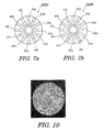
- This limitation on the angles is described by referring to the Ronchigram of FIG. 10 .
- This diagram is obtained when an electron beam passing through a single stage of multipole element is corrected for aberrations, the multipole element producing a magnetic field of 3-fold symmetry with respect to the optical axis.
- a low-contrast region appearing in the center of the diagram corresponds to the angle of incidence of the electron beam on the multipole element, the beam being appropriately corrected for aberrations.
- the central region of low contrast is hexagonal, because 6-fold astigmatism appearing at the fifth-order aberration remains.
- the angle of incidence of the electron beam that can be corrected for aberrations is 50 mrad at maximum. It is difficult to appropriately correct the electron beam having a greater angle of incidence for aberrations. Accordingly, if one tries to reduce diffraction aberration, the spatial resolution is limited due to the limitation on the angle of incidence.
- the 6-fold astigmatism can be corrected by a dodecapole (12-pole) element where magnetic poles of N and S poles are alternately arranged.
- the rotation may be achieved using a 24-pole element but this element involves difficulties, such as low machining accuracy and low assembly accuracy.
- the coil that is necessary for correction of 6-fold astigmatism needs to have a number of turns of winding comparable to or greater than the number of turns of winding on the coil used for correction of spherical aberration. Where the coil of this design is installed on each pole to obtain a magnetic pole, it is very difficult to secure a space.
- an object of the present invention to provide an aberration corrector which is adapted for use with a charged-particle beam system and which is simple in structure but can correct both spherical aberration and 6-fold astigmatism.
- a first embodiment of the present invention provides an aberration corrector for correcting aberrations in a charged-particle beam.
- the corrector has two stages of dodecapole elements and exciting coils installed respectively at the poles of the dodecapole elements.
- the exciting coils of the (4n+1)th pole and the exciting coils of the (4n+4)th pole are alternately connected in series and produce magnetic fields which are identical in absolute value but mutually opposite in sense relative to the optical axis within a plane perpendicular to the optical axis.
- the exciting coils of the (4n+3)th pole and the exciting coils of the (4n+2)th pole are alternately connected in series and produce magnetic fields which are identical in absolute value but mutually opposite in sense relative to the optical axis within the plane perpendicular to the optical axis. Consequently, a superimposition of magnetic fields of 3-fold symmetry and magnetic fields of 6-fold symmetry is produced.
- a second embodiment of the present invention provides an aberration corrector which is based on the aberration corrector of the first embodiment and further characterized in that each pole of the dodecapole elements serves also as an electrode.
- the (4m+1)th poles are all electrically connected.
- the (4m+2)th poles are all electrically connected.
- the (4m+3)th poles are all electrically connected.
- the (4m+4)th poles are all electrically connected.
- the (4m+1)th poles and the (4m+4)th poles produce electric fields which are identical in absolute value but mutually opposite in sense relative to the optical axis within the plane perpendicular to the optical axis.
- the (4m+2)th poles and the (4m+3)th poles produce electric fields which are identical in absolute value but mutually opposite in sense relative to the optical axis within the plane perpendicular to the axis. Consequently, a superimposition of electric fields of 3-fold symmetry and electric fields of 6-fold symmetry is produced.
- a third embodiment of the present invention provides an aberration corrector for correcting aberrations in a charged-particle beam.
- the (4s+1)th poles are all electrically connected.
- the (4s+2)th poles are all electrically connected.
- the (4s+3)th poles are all electrically connected.
- the (4s+4)th poles are all electrically connected.
- the (4s+1)th poles and the (4s+4)th poles produce electric fields which are identical in absolute value but mutually opposite in sense relative to the optical axis within a plane perpendicular to the optical axis.
- the (4s+2)th poles and the (4s+3)th poles produce electric fields which are identical in absolute value but mutually opposite in sense relative to the optical axis within the plane perpendicular to the axis. Consequently, a superimposition of electric fields of 3-fold symmetry and electric fields of 6-fold symmetry is produced.
- a fourth embodiment of the present invention provides a charged-particle beam system equipped with the aberration corrector of the first embodiment.
- a fifth embodiment of the present invention provides a charged-particle beam system equipped with the aberration corrector of the second embodiment.
- a sixth embodiment of the present invention provides a charged-particle beam system equipped with the aberration corrector of the third embodiment.
- spherical aberration and 6-fold astigmatism can be corrected at the same time with a simple structure.
- a probe having a wider angular aperture can be created. Therefore, diffraction aberration is reduced.
- a probe having a quite small diameter can be produced. Also, improved spatial resolution can be accomplished.
- FIG. 1 is a schematic representation of one example of a configuration of the aberration corrector, according to the present invention
- FIG. 2 is a schematic representation of a dodecapole element associated with a first embodiment of the present invention
- FIGS. 3 a and 3 b show electric circuits associated with the first embodiment of the present invention
- FIGS. 4 a , 4 b , 4 c , and 4 d show diagrams showing the polarities of the poles of the dodecapole element associated with the first embodiment of the present invention when the dodecapole element is excited, and in which FIGS. 4 a and 4 c show cases where magnetic fields of 3-fold symmetry are produced and FIGS. 4 b and 4 d show cases where magnetic fields of 6-fold symmetry are produced;
- FIG. 5 is a schematic representation of a dodecapole element associated with a second embodiment of the present invention.
- FIGS. 6 a and 6 b show electric circuits associated with the second embodiment of the present invention.
- FIGS. 7 a and 7 b show diagrams showing the polarities of the poles of the dodecapole element associated with the second embodiment of the present invention when voltages are applied to the dodecapole element, and in which FIG. 7 a shows a case where electric fields of 3-fold symmetry are produced and FIG. 7 b shows a case where electric fields of 6-fold symmetry are produced;
- FIG. 8 shows a modification of the aberration corrector of the present invention
- FIG. 9 is a schematic block diagram of a transmission electron microscope equipped with an aberration corrector associated with the present invention.
- FIG. 10 is a Ronchigram obtained by passing an electron beam through two stages of multipole elements each having a thickness along the optical axis.
- a 6 A 3 2 ⁇ ⁇ A 3 ⁇ 2 14 ⁇ M 6 ⁇ f 6 ⁇ t 7 ( 1 )
- a 6 is a 6-fold astigmatism coefficient per unit length
- a 3 is a 3-fold astigmatism coefficient per unit length
- M is a demagnification factor achieved by the two stages of multipole elements and objective lens
- t is the thickness of each multipole element taken along the optical axis
- f the focal length of the objective lens.
- Let a 3 be the strength of 3-fold astigmatism.
- ⁇ a3 be the azimuthal angle of 3-fold astigmatism.
- 6-fold astigmatisms can be corrected or reduced if magnetic fields producing 6-fold astigmatisms at twice closer intervals than magnetic fields producing 3-fold astigmatisms without any phase relationship therebetween (i.e., with no phase difference) are used.
- a dodecapole element is used as a multipole element producing both types of magnetic fields.
- Six-fold astigmatisms can be corrected or reduced by using 6 poles of the dodecapole element to produce 3-fold astigmatisms and using all the 12 poles to produce 6-fold astigmatisms. Both types of magnetic fields can be produced by a combination of exciting coils mounted at the poles of the dodecapole element as described later.
- the magnetic fields may be replaced by electric fields.
- each of the magnetic fields may be a superimposition of a magnetic field and an electric field. Where the electric fields are set up, each pole of the dodecapole element acts as an electrode. Where superimposed electric and magnetic fields are produced, each pole is used in combination with an exciting coil such that each pole acts as a magnetic pole and an electrode. As a result, the same advantages can be obtained as where only magnetic fields are used.
- FIG. 1 is a schematic representation of one example of configuration of the aberration corrector, according to the present invention.
- FIG. 2 is a schematic representation of a dodecapole element associated with a first embodiment of the present invention.
- FIGS. 3 a and 3 b show electric circuits associated with the first embodiment of the present invention.
- FIGS. 4 a , 4 b , 4 c , and 4 d show diagrams showing the polarities of the poles of the dodecapole element associated with the first embodiment of the present invention when the dodecapole element is excited.
- FIGS. 4 a and 4 c show cases where magnetic fields of 3-fold symmetry are produced.
- FIGS. 4 b and 4 d show cases where magnetic fields of 6-fold symmetry are produced.
- the aberration corrector 10 of the present embodiment has two stages of dodecapole elements 12 and 13 arrayed along the optical axis 11 of an electron beam.
- the dodecapole elements 12 and 13 have thicknesses of t 1 and t 2 , respectively, taken in the direction of the optical axis.
- the thicknesses may be identical or different.
- each of the dodecapole elements 12 and 13 has 12 poles 31 a - 31 l arranged radially about the optical axis 11 . That is, the poles 31 a - 31 l are spaced from each other about the optical axis 11 at intervals of 30°. Exciting coils 32 a - 32 l are arranged on the poles, respectively, to produce static magnetic fields of 3-fold symmetry about the optical axis 11 , as well as static magnetic fields of 6-fold symmetry superimposed on the fields of 3-fold symmetry.
- each exciting coil is shown in FIGS. 3 a and 3 b .
- the exciting coils 32 a , 32 d , 32 e , 32 h , 32 i , and 32 l are connected in series with a power supply 33 to form a circuit 35 .
- the exciting coils 32 a , 32 e , and 32 i produce magnetic fields B 1 , B 5 , and B 9 which are identical in sense relative to the optical axis 11 and in strength within a plane perpendicular to the optical axis 11 .
- the magnetic fields B 1 , B 5 , and B 9 are distributed at intervals of 120° about the optical axis 11 within the plane perpendicular to the optical axis 11 .
- the exciting coils 32 d , 32 h , and 32 l produce magnetic fields B 4 , B 8 , and B 12 which are identical in sense relative to the optical axis 11 and in strength within the plane perpendicular to the optical axis 11 .
- the fields B 4 , B 8 , and B 12 are opposite in sense to the magnetic fields B 1 , B 5 , and B 9 produced by the exciting coils 32 a , 32 e , and 32 i .
- the magnetic fields B 4 , B 8 , and B 12 are distributed at intervals of 120° about the optical axis 11 within the plane perpendicular to the axis 11 .
- the power supply 33 is of the bipolar output type capable of varying the direction of current at will.
- exciting coils 32 b , 32 c , 32 f , 32 g , 32 j , and 32 k are connected in series with a power supply 34 to form a circuit 36 .
- the exciting coils 32 b , 32 f , and 32 j produce magnetic fields B 2 , B 6 , and B 10 , respectively, which are identical in sense relative to the optical axis 11 and in strength within the plane perpendicular to the optical axis 11 .
- the magnetic fields B 2 , B 6 , and B 10 are distributed at intervals of 120° about the optical axis 11 within the plane perpendicular to the axis 11 .
- the exciting coils 32 c , 32 g , and 32 k develop magnetic fields B 3 , B 7 , and B 11 that are identical in sense relative to the optical axis 11 and in strength within the plane perpendicular to the optical axis 11 but the fields B 3 , B 7 , and B 11 are opposite in sense to the magnetic fields B 2 , B 6 , and B 10 produced by the exciting coils 32 b , 32 f , and 32 j .
- the magnetic fields B 3 , B 7 , and B 11 are distributed at intervals of 120° about the optical axis 11 within the plane perpendicular to the axis 11 .
- each of the dodecapole elements 12 and 13 are made of the two circuits 35 and 36 .
- the senses of the magnetic fields shown in FIGS. 3 a and 3 b depend on the directions of the currents flowing from the power supplies 33 and 34 . Therefore, it is obvious that magnetic fields opposite in sense to those shown in FIGS. 3 a and 3 b can be produced.
- each of the dodecapole elements 12 and 13 has a reference pole such as pole 31 a .
- This reference pole is referred to as the first pole.
- the dodecapole element has first through twelfth poles arranged in this order.
- the exciting coils of the (4n+1)th poles and the exciting coils of the (4n+4)th poles are alternately connected in series and produce magnetic fields which are identical in absolute value but opposite in sense relative to the optical axis within the plane perpendicular to the optical axis.
- the exciting coils of the (4n+3)th poles and the exciting coils of the (4n+2)th poles are alternately connected in series and produce magnetic fields which are identical in absolute value but mutually opposite in sense relative to the optical axis within the plane perpendicular to the axis.
- each exciting coil is not connected with a separate power supply but energized by a common power supply.
- magnetic fields that are identical in sense relative to the optical axis 11 and in strength are produced at intervals of 120° about the optical axis 11 . Because of this 3-fold symmetry, if the power supply output lacks stability, non-rotationally symmetric shapes of the electron beam rarely appear. That is, the shape of the electron beam is stabilized.
- the dodecapole elements 12 and 13 having such circuits can produce the magnetic fields of 3-fold symmetry and the magnetic fields of 6-fold symmetry at the same time.
- the circuit 35 is electrically energized such that the poles 31 a , 31 e , and 31 i are polarized north. Then, the poles 31 d , 31 h , and 31 l are polarized south.
- the circuit 36 is electrically energized so that the poles 31 b , 31 f , and 31 j are polarized north. Consequently, the poles 31 c , 31 g , and 31 k are polarized south.
- magnetic poles (NNSSNNSSNNSS) are arranged in turn from the pole 31 a to pole 31 l about the optical axis 11 . As a consequence, magnetic fields of 3-fold symmetry are produced.
- the poles 31 a , 31 e , and 31 i are polarized south.
- the poles 31 d , 31 h , and 31 l are polarized north. Accordingly, the magnetic poles (SNSNSNSNSN) are arrayed in order from the pole 31 a to pole 31 l around the optical axis 11 as shown in FIG. 4 b . Consequently, magnetic fields of 6-fold symmetry are produced.
- the polarities of the magnetic fields of 3-fold symmetry can be reversed.
- the magnetic fields of 3-fold symmetry are rotated through 60° about the optical axis 11 .
- the circuit 35 is electrically energized so that the poles 31 a , 31 e , and 31 i are polarized south.
- the poles 31 d , 31 h , and 31 l are polarized north.
- the circuit 36 is electrically energized so that the poles 31 b , 31 f , and 31 j are polarized south.
- the poles 31 c , 31 g , and 31 k are polarized north.
- the magnetic poles are arrayed in turn from the poles 31 a to the pole 31 l around the optical axis 11 .
- Magnetic fields of 3-fold symmetry having polarities opposite to the foregoing polarities are produced as shown in FIG. 4 c .
- the circuit 35 is energized with an electrical current in the opposite direction.
- Magnetic poles (NSNSNSNSNSNS) arrayed from the pole 31 a to the pole 31 l as shown in FIG. 4 d are produced.
- These are magnetic fields of 6-fold symmetry having polarities opposite to the foregoing polarities. In other words, the aforementioned magnetic fields of 6-fold symmetry are rotated through 30°.
- the 6-fold astigmatism can be corrected without rotating the dodecapole element 12 or 13 about the optical axis 11 .
- positive spherical aberration produced in the objective lens can be corrected.
- transfer lenses 14 a and 14 b of a pair having transfer magnification of 1:1 may be mounted between the dodecapole elements 12 and 13 as shown in FIG. 8 .
- Transfer lenses 15 a and 15 b of a pair having transfer magnification of 1:1 may be mounted between an objective lens 16 and the dodecapole element 13 .
- the transfer lenses 14 a and 14 b of the pair transfer a reciprocal space image of an electron beam 17 formed in the dodecapole element 12 to the dodecapole element 13 . Furthermore, the transfer lenses 15 a and 15 b of the pair transfer the reciprocal space image of the electron beam 17 appearing in the dodecapole element 13 to a coma-free plane 16 a of the objective lens. This plane is substantially identical with the front focal plane of the objective lens.
- the reciprocal space image transferred to the coma-free plane 16 a becomes a real space image on a sample surface 16 b of the objective lens.
- FIG. 5 is a schematic representation of a dodecapole element associated with the second embodiment of the present invention.
- FIGS. 6 a and 6 b show electric circuits associated with the second embodiment of the present invention.
- FIGS. 7 a and 7 b show diagrams showing the polarities of the poles of the dodecapole element associated with the second embodiment of the present invention when voltages are applied to the dodecapole element.
- FIG. 7 a shows a case where electric fields of 3-fold symmetry are produced
- FIG. 7 b shows a case where electric fields of 6-fold symmetry are produced.
- An aberration corrector 20 associated with the second embodiment of the present invention has two stages of dodecapole elements 22 and 23 arrayed along the optical axis 11 of an electron beam as shown in FIG. 1 .
- the dodecapole elements 22 and 23 have thicknesses of t 1 and t 2 , respectively, taken in the direction of the optical axis.
- the thicknesses may be identical or different.
- the dodecapole elements 22 and 23 associated with the present embodiment are arranged relative to the optical axis 11 in the same way as in the first embodiment as shown in FIG. 1 .
- the configuration is more particularly shown in FIG. 5 , where poles 41 a - 41 l are arranged radially about the optical axis 11 .
- the poles 41 a - 41 l are arranged at intervals of 30° about the optical axis 11 .
- a power supply 43 or 44 is connected with each of the poles 41 a - 41 l , and a voltage is applied to each pole.
- static electric fields of 3-fold symmetry and static magnetic fields of 6-fold symmetry are produced about the optical axis 11 , the latter fields being superimposed on the former fields.
- FIGS. 6 a and 6 b One example of wire connection of each pole is shown in FIGS. 6 a and 6 b .
- the three poles 41 a , 41 e , and 41 i are connected to one output of the power supply 43 .
- the three poles 41 d , 41 h , and 41 l are connected with the other output of the power supply 43 .
- a circuit 45 is formed.
- the poles 41 a , 41 e , and 41 i are at equipotential and produce electric fields that are identical in sense relative to the optical axis 11 and in strength within the plane perpendicular to the optical axis 11 .
- the poles 41 d , 41 h , and 41 l are at equipotential and produce magnetic fields that are identical in sense relative to the optical axis 11 and in strength within the plane perpendicular to the axis 11 .
- their polarities are opposite to the senses of the electric fields produced by the poles 41 a , 41 e , and 41 i . That is, in the circuit 45 shown in FIG. 6 a , the senses of the electric fields produced by the poles are alternately faced away from the optical axis 11 within the plane perpendicular to the optical axis 11 .
- the power supply 43 is of the bipolar output type capable of varying the direction of output at will.
- poles 41 b , 41 c , 41 f , 41 g , 41 j , and 41 k are connected in series with the power supply 44 to form a circuit 46 .
- the poles 41 b , 41 f , and 41 j produce magnetic fields that are identical in sense relative to the optical axis 11 and in strength within the plane perpendicular to the axis 11 .
- the poles 41 c , 41 g , and 41 k produce magnetic fields which are identical in sense relative to the optical axis 11 and in strength within the plane perpendicular to the axis 11 .
- the senses of the magnetic fields are opposite to the senses of the magnetic fields produced by the poles 41 b , 41 f , and 41 j . That is, in the circuit shown in FIG. 6 b , the senses of the magnetic fields produced by the poles are alternately faced away from the optical axis 11 within the plane perpendicular to the axis.
- the power supply 44 is of the bipolar output type capable of varying the polarity of the output voltage at will. As described so far, each of the dodecapole elements 22 and 23 is made up of the two circuits 45 and 46 .
- each of the dodecapole elements 22 and 23 has a reference pole such as pole 41 a .
- This reference pole is referred to as the first pole.
- the dodecapole element has first through twelfth poles arranged in this order.
- the (4s+1)th poles are all electrically connected.
- the (4s+4)th poles are all electrically connected.
- the (4s+1)th poles and the (4s+4)th poles produce electric fields which are identical in absolute value but mutually opposite in sense relative to the optical axis 11 within the plane perpendicular to the axis 11 .
- the potentials at the (4s+1)th and (4s+4)th poles are identical in absolute value but different in polarity.
- the (4s+2)th poles are all electrically connected.
- the (4s+3)th poles are all electrically connected.
- the (4s+2)th poles and the (4s+3)th poles produce electric fields which are identical in absolute value but mutually opposite in sense relative to the optical axis 11 within the plane perpendicular to the axis 11 . That is, the potentials at the (4s+2)th and (4s+3)th poles are identical in absolute value but different in polarity.
- each pole is not connected with a separate power supply but applied with a voltage from a common power supply. Electric fields that are identical in sense and strength are produced at intervals of 120° about the optical axis 11 . Because of this 3-fold symmetry, if the power supply output lacks stability, non-rotationally symmetric shapes of the electron beam rarely appear. That is, the shape of the electron beam is stabilized.
- the dodecapole elements 22 and 23 having such circuits can produce the electric fields of 3-fold symmetry and the electric fields of 6-fold symmetry at the same time.
- voltages are applied such that the poles 41 a , 41 e , and 41 i are polarized positively (+) and that the poles 41 d , 41 h , and 41 l are polarized negatively ( ⁇ ).
- voltages are applied such that the poles 41 b , 41 f , and 41 j are polarized positively (+) and that the poles 41 c , 41 g , and 41 k are polarized negatively ( ⁇ ).
- electrodes of (++ ⁇ ++ ⁇ ++ ⁇ ) are arranged in turn from the pole 41 a to the pole 41 l around the optical axis 11 .
- electric fields of 3-fold symmetry are produced.
- the poles 41 a , 41 e , and 41 i are polarized negatively ( ⁇ ).
- the poles 41 d , 41 h , and 41 l are polarized positively (+). Accordingly, the electrodes of ( ⁇ + ⁇ + ⁇ + ⁇ + ⁇ + ⁇ + ⁇ +) are arrayed in turn from the pole 41 a to pole 41 l around the optical axis 11 as shown in FIG. 7 b . Consequently, electric fields of 6-fold symmetry are produced.
- the polarities of the electric fields of 3-fold symmetry can be reversed.
- the electric fields of 3-fold symmetry are rotated through 60° about the optical axis 11 .
- voltages are applied such that the poles 41 a , 41 e , and 41 i are polarized negatively ( ⁇ ) and that the poles 41 d , 41 h , and 41 l are polarized positively (+).
- voltages are applied such that the poles 41 b , 41 f , and 41 j are polarized negatively ( ⁇ ) and that the poles 41 c , 41 g , and 41 k are polarized positively (+).
- Electrodes of ( ⁇ ++ ⁇ ++ ⁇ ++) are arrayed in turn from the pole 41 a to the pole 41 l around the optical axis 11 .
- Electric fields of 3-fold symmetry of the polarities opposite to the polarities shown in FIG. 7 a are produced. Under this condition, if the output polarity of the power supply 43 is reversed, polarities + ⁇ + ⁇ + ⁇ + ⁇ + ⁇ + ⁇ + ⁇ are arrayed in turn from the pole 41 a to the pole 41 l .
- Electric fields of 6-fold symmetry of the polarities opposite to the polarities shown in FIG. 7 b are produced.
- electric fields of 6-fold symmetry having the polarities opposite to the polarities of the foregoing fields are produced. In other words, the aforementioned electric fields of 6-fold symmetry are rotated through 30°.
- the 6-fold astigmatism can be corrected without rotating the dodecapole element 12 or 13 about the optical axis 11 .
- positive spherical aberration produced in the objective lens can be corrected.
- transfer lenses 14 a and 14 b of a pair having transfer magnification of 1:1 may be mounted between the dodecapole elements 22 and 23 as shown in FIG. 8 .
- Transfer lenses 15 a and 15 b of a pair having transfer magnification of 1:1 may be mounted between the objective lens 16 and dodecapole element 23 , in the same way as in the first embodiment.
- a third embodiment of the present invention is a combination of the aberration corrector 10 of the first embodiment and the aberration corrector 20 of the second embodiment.
- Two stages of dodecapole elements for producing magnetic and electric fields of 3-fold symmetry and magnetic and electric fields of 6-fold symmetry are produced around the optical axis 11 to correct 6-fold astigmatism and spherical aberration.
- the power supplies 43 and 44 shown in FIGS. 6 a and 6 b are connected with the poles 31 a - 31 l of the dodecapole elements 12 and 13 (see FIGS. 1 and 2 ) described in the first embodiment. Consequently, the magnetic fields of 3-fold symmetry and 6-fold symmetry described in the first embodiment and the electric fields of 3-fold symmetry and 6-fold symmetry described in the second embodiment can be superimposed. Hence, advantages identical with the advantages of the first and second embodiments can be gained.
- the two magnetic fields and the two electric fields can have any desired rotational symmetry.
- the poles with which the power supplies 43 and 44 are connected are not limited to the poles shown in FIGS. 6 a and 6 b.
- each of the dodecapole elements 12 and 13 of the first embodiment has first through twelfth poles arranged in this order.
- Any desired pole (such as pole 31 a ) is referred to as the first pole.
- the (4m+1)th poles are all electrically connected.
- the (4m+4)th poles are all electrically connected.
- the (4m+1)th and (4m+4)th poles produce electric fields which are identical in absolute value but mutually opposite in sense relative to the optical axis within the plane perpendicular to the axis.
- the potentials at the (4m+1)th poles and at the (4m+4)th poles are identical in absolute value but different in polarity.
- the (4m+2)th poles are all electrically connected.
- the (4m+3)th poles are all electrically connected.
- the (4m+2)th and (4m+3)th poles produce electric fields which are identical in absolute value but mutually opposite in sense relative to the optical axis within the plane perpendicular to the optical. That is, the potentials at the (4m+2)th and (4m+3)th poles are identical in absolute value but different in polarity.
- the two pairs of transfer lenses 14 a , 14 b , 15 a , 15 b described in the first and second embodiments may be mounted (see FIG. 8 ). As a result, advantages identical with the advantages of the first and second embodiments can be obtained.
- FIG. 9 shows one example of a charged-particle beam system associated with the fourth embodiment.
- This system is a transmission electron microscope 60 in which an aberration corrector associated with any one of the first through third embodiments is used as an aberration corrector 63 of the illumination system.
- the microscope has an electron gun 61 producing an electron beam (not shown) and accelerating it to a desired energy under control of a high-voltage control portion 68 .
- the accelerated electron beam is converged by a first condenser lens 62 and a second condenser lens 64 .
- the beam is further converged in an objective lens and sample stage 65 and directed at a sample placed on the sample stage.
- the aberration corrector 63 of the illumination system mounted between the first condenser lens 62 and the second condenser lens 64 produces magnetic or electric fields of 3-fold symmetry and magnetic or electric fields of 6-fold symmetry, the latter fields being superimposed on the former fields.
- this aberration corrector has negative spherical aberration and so cancels out positive spherical aberration induced by the objective lens. Furthermore, 6-fold astigmatism is corrected.
- the electron beam transmitted through the sample is magnified by an intermediate projector lens 66 and made to impinge on a fluorescent screen (not shown) in an observation chamber 67 .
- the sample image projected onto the fluorescent screen is captured by a camera or other device.
- the spatial resolution of the transmission electron microscope 60 is improved.
- the aberration correction using the aberration corrector 63 of the illumination system extends the range of incident angles of the electron beam in which aberrations can be corrected. If the range of angles of the electron beam is extended, diffraction aberration due to an aperture (not shown) is reduced. Therefore, the spatial resolution of the transmission electron microscope is improved further.
- an aberration corrector (not shown) of similar structure may be mounted behind the objective lens.
- both aberration correctors may be installed.
- the aberration corrector of the present invention can be installed in every type of charged-particle beam system in which spherical aberration and 6-fold astigmatism are required to be corrected.
- the aberration corrector can be installed in a scanning electron microscope, scanning transmission electron microscope, ion microscope, focused ion beam system, and so on, as well as in the above-described transmission electron microscope.
Landscapes
- Chemical & Material Sciences (AREA)
- Analytical Chemistry (AREA)
- Electron Sources, Ion Sources (AREA)
- Electron Beam Exposure (AREA)
- Electron Tubes For Measurement (AREA)
Abstract
Description
where A6 is a 6-fold astigmatism coefficient per unit length, A3 is a 3-fold astigmatism coefficient per unit length, M is a demagnification factor achieved by the two stages of multipole elements and objective lens, t is the thickness of each multipole element taken along the optical axis, and f is the focal length of the objective lens. Let a3 be the strength of 3-fold astigmatism. Let θa3 be the azimuthal angle of 3-fold astigmatism. The 3-fold astigmatism coefficient A3 can be represented by
A 3 =a 3 exp(3iθ a3) (2)
and so it can be seen that there exists a certain angular relationship between the 3-fold astigmatism coefficient A3 and 6-fold astigmatism coefficient A6, the relationship being given by
A 6∝(a 3)4 exp(6iθ a3) (3)
That is, we take notice of variations in the coefficients A3 and A6 when the azimuthal angle θa3 of 3-fold astigmatism is varied. Six-fold astigmatisms are produced all about the origin (i.e., about the optical axis) at twice closer intervals than the intervals of the produced 3-fold astigmatisms. Consequently, 6-fold astigmatisms can be corrected or reduced if magnetic fields producing 6-fold astigmatisms at twice closer intervals than magnetic fields producing 3-fold astigmatisms without any phase relationship therebetween (i.e., with no phase difference) are used. Accordingly, a dodecapole element is used as a multipole element producing both types of magnetic fields. Six-fold astigmatisms can be corrected or reduced by using 6 poles of the dodecapole element to produce 3-fold astigmatisms and using all the 12 poles to produce 6-fold astigmatisms. Both types of magnetic fields can be produced by a combination of exciting coils mounted at the poles of the dodecapole element as described later.
Claims (6)
Applications Claiming Priority (2)
| Application Number | Priority Date | Filing Date | Title |
|---|---|---|---|
| JP2008244927A JP5237734B2 (en) | 2008-09-24 | 2008-09-24 | Aberration correction apparatus and charged particle beam apparatus including the aberration correction apparatus |
| JP2008-244927 | 2008-09-24 |
Publications (2)
| Publication Number | Publication Date |
|---|---|
| US20100072387A1 US20100072387A1 (en) | 2010-03-25 |
| US9793088B2 true US9793088B2 (en) | 2017-10-17 |
Family
ID=41505898
Family Applications (1)
| Application Number | Title | Priority Date | Filing Date |
|---|---|---|---|
| US12/564,277 Active 2031-07-28 US9793088B2 (en) | 2008-09-24 | 2009-09-22 | Two-stage dodecapole aberration corrector for charged-particle beam |
Country Status (4)
| Country | Link |
|---|---|
| US (1) | US9793088B2 (en) |
| EP (1) | EP2169702B1 (en) |
| JP (1) | JP5237734B2 (en) |
| AT (1) | ATE532202T1 (en) |
Cited By (1)
| Publication number | Priority date | Publication date | Assignee | Title |
|---|---|---|---|---|
| US20220415605A1 (en) * | 2019-11-21 | 2022-12-29 | Hitachi High-Tech Corporation | Charged Particle Beam Device and Aberration Correction Method |
Families Citing this family (17)
| Publication number | Priority date | Publication date | Assignee | Title |
|---|---|---|---|---|
| JP3064586B2 (en) | 1991-10-15 | 2000-07-12 | 富士ゼロックス株式会社 | Interlace scanning circuit |
| JP5502595B2 (en) * | 2010-05-18 | 2014-05-28 | 日本電子株式会社 | Spherical aberration correction apparatus and spherical aberration correction method |
| JP5677081B2 (en) * | 2010-12-28 | 2015-02-25 | 株式会社日立ハイテクノロジーズ | Charged particle beam equipment |
| DE102011009954A1 (en) * | 2011-02-01 | 2012-08-02 | Ceos Corrected Electron Optical Systems Gmbh | proofreader |
| US8536538B2 (en) * | 2011-02-16 | 2013-09-17 | Kla-Tencor Corporation | Multiple-pole electrostatic deflector for improving throughput of focused electron beam instruments |
| WO2012112894A2 (en) * | 2011-02-18 | 2012-08-23 | Applied Materials Israel, Ltd. | Focusing a charged particle imaging system |
| CN102867546B (en) * | 2012-09-11 | 2015-01-21 | 中国科学技术大学 | Device with simplified 12-electrode-field magnet and manufacturing method thereof |
| CN103345957B (en) * | 2013-06-26 | 2015-10-21 | 中国科学技术大学 | A kind of Circular Aperture antisymmetry simplifies hexapole field magnet arrangement and manufacture method thereof |
| JP6254445B2 (en) | 2014-01-09 | 2017-12-27 | 株式会社日立ハイテクノロジーズ | Charged particle beam equipment |
| CN104681230B (en) * | 2014-12-16 | 2017-03-29 | 中国原子能科学研究院 | A kind of accelerator line homogenization six pole magnet |
| JP6326380B2 (en) * | 2015-01-20 | 2018-05-16 | 日本電子株式会社 | Multipole lens and charged particle beam device |
| US9922796B1 (en) * | 2016-12-01 | 2018-03-20 | Applied Materials Israel Ltd. | Method for inspecting a specimen and charged particle multi-beam device |
| US10453645B2 (en) | 2016-12-01 | 2019-10-22 | Applied Materials Israel Ltd. | Method for inspecting a specimen and charged particle multi-beam device |
| JP6868480B2 (en) * | 2017-06-20 | 2021-05-12 | 日本電子株式会社 | Distortion correction method and electron microscope |
| JP7124216B2 (en) * | 2019-05-15 | 2022-08-23 | 株式会社日立ハイテク | Charged particle beam device |
| US11056312B1 (en) * | 2020-02-05 | 2021-07-06 | Kla Corporation | Micro stigmator array for multi electron beam system |
| US11239045B1 (en) * | 2020-09-30 | 2022-02-01 | Fei Company | Method and system for correcting two-fold, fifth-order parasitic aberrations in charged particle systems |
Citations (14)
| Publication number | Priority date | Publication date | Assignee | Title |
|---|---|---|---|---|
| US4962309A (en) * | 1989-08-21 | 1990-10-09 | Rockwell International Corporation | Magnetic optics adaptive technique |
| US20020121609A1 (en) * | 2000-07-25 | 2002-09-05 | Jeol Ltd. | Stigmator assembly |
| US20030043358A1 (en) * | 2001-08-31 | 2003-03-06 | Nikon Corporation | Methods for determining focus and astigmatism in charged-particle-beam microlithography |
| US20040227099A1 (en) * | 2003-02-14 | 2004-11-18 | Jeol Ltd. | Charged-particle optical system |
| US20050029466A1 (en) * | 2003-06-24 | 2005-02-10 | Jeol Ltd. | Multipole lens, charged-particle beam instrument fitted with multipole lenses, and method of fabricating multipole lens |
| US20060169900A1 (en) * | 2003-04-22 | 2006-08-03 | Ebara Corporation | Testing apparatus using charged particles and device manufacturing method using the testing apparatus |
| US20070114403A1 (en) * | 2005-09-27 | 2007-05-24 | Jeol Ltd. | Electron microscope |
| US20070114408A1 (en) * | 2005-11-01 | 2007-05-24 | Jeol Ltd. | Charged-particle beam system |
| US20070181806A1 (en) * | 2006-02-03 | 2007-08-09 | Tomonori Nakano | Charged particle optical apparatus with aberration corrector |
| US20070284524A1 (en) * | 2006-04-06 | 2007-12-13 | Bruker Daltonik Gmbh | Rf multipole ion guides for broad mass range |
| US20080054186A1 (en) * | 2006-08-31 | 2008-03-06 | Jeol Ltd. | Method of Aberration Correction and Electron Beam System |
| US20090014649A1 (en) * | 2005-03-22 | 2009-01-15 | Ebara Corporation | Electron beam apparatus |
| US20100264335A1 (en) * | 2007-07-31 | 2010-10-21 | Vistec Lithography Inc. | Pattern writing on a rotating substrate |
| US20120056085A1 (en) * | 2009-05-01 | 2012-03-08 | Shimadzu Research Laboratory (Europe) Limited | Ion analysis apparatus and method of use |
Family Cites Families (9)
| Publication number | Priority date | Publication date | Assignee | Title |
|---|---|---|---|---|
| JPS4618114Y1 (en) * | 1967-10-17 | 1971-06-24 | ||
| EP0451370B1 (en) * | 1990-04-12 | 1996-03-27 | Koninklijke Philips Electronics N.V. | Correction system for a charged-particle beam apparatus |
| JPH11219678A (en) * | 1998-01-30 | 1999-08-10 | Nikon Corp | Aberration correction method for charged particle beam device and charged particle beam device |
| JP3914750B2 (en) * | 2001-11-20 | 2007-05-16 | 日本電子株式会社 | Charged particle beam device with aberration correction device |
| JP2004095489A (en) * | 2002-09-04 | 2004-03-25 | Jeol Ltd | Vienna filter |
| JP4313691B2 (en) * | 2003-02-14 | 2009-08-12 | 日本電子株式会社 | Charged particle optics |
| JP4328192B2 (en) * | 2003-12-12 | 2009-09-09 | 日本電子株式会社 | Multipole field generating device and aberration correcting device in charged particle optical system |
| JP2005183021A (en) * | 2003-12-16 | 2005-07-07 | Jeol Ltd | Energy analyzer |
| US8242457B2 (en) * | 2007-03-15 | 2012-08-14 | Multibeam Corporation | Charged particle optics with azimuthally-varying third-order aberrations for generation of shaped beams |
-
2008
- 2008-09-24 JP JP2008244927A patent/JP5237734B2/en active Active
-
2009
- 2009-09-17 AT AT09252208T patent/ATE532202T1/en active
- 2009-09-17 EP EP09252208A patent/EP2169702B1/en active Active
- 2009-09-22 US US12/564,277 patent/US9793088B2/en active Active
Patent Citations (14)
| Publication number | Priority date | Publication date | Assignee | Title |
|---|---|---|---|---|
| US4962309A (en) * | 1989-08-21 | 1990-10-09 | Rockwell International Corporation | Magnetic optics adaptive technique |
| US20020121609A1 (en) * | 2000-07-25 | 2002-09-05 | Jeol Ltd. | Stigmator assembly |
| US20030043358A1 (en) * | 2001-08-31 | 2003-03-06 | Nikon Corporation | Methods for determining focus and astigmatism in charged-particle-beam microlithography |
| US20040227099A1 (en) * | 2003-02-14 | 2004-11-18 | Jeol Ltd. | Charged-particle optical system |
| US20060169900A1 (en) * | 2003-04-22 | 2006-08-03 | Ebara Corporation | Testing apparatus using charged particles and device manufacturing method using the testing apparatus |
| US20050029466A1 (en) * | 2003-06-24 | 2005-02-10 | Jeol Ltd. | Multipole lens, charged-particle beam instrument fitted with multipole lenses, and method of fabricating multipole lens |
| US20090014649A1 (en) * | 2005-03-22 | 2009-01-15 | Ebara Corporation | Electron beam apparatus |
| US20070114403A1 (en) * | 2005-09-27 | 2007-05-24 | Jeol Ltd. | Electron microscope |
| US20070114408A1 (en) * | 2005-11-01 | 2007-05-24 | Jeol Ltd. | Charged-particle beam system |
| US20070181806A1 (en) * | 2006-02-03 | 2007-08-09 | Tomonori Nakano | Charged particle optical apparatus with aberration corrector |
| US20070284524A1 (en) * | 2006-04-06 | 2007-12-13 | Bruker Daltonik Gmbh | Rf multipole ion guides for broad mass range |
| US20080054186A1 (en) * | 2006-08-31 | 2008-03-06 | Jeol Ltd. | Method of Aberration Correction and Electron Beam System |
| US20100264335A1 (en) * | 2007-07-31 | 2010-10-21 | Vistec Lithography Inc. | Pattern writing on a rotating substrate |
| US20120056085A1 (en) * | 2009-05-01 | 2012-03-08 | Shimadzu Research Laboratory (Europe) Limited | Ion analysis apparatus and method of use |
Non-Patent Citations (3)
| Title |
|---|
| A.V.Crewe and D. Kopf, "A sextupole system for the correction of spherical aberration," Optik, vol. 55, No. 1 (1980), pp. 1-10. |
| Fumio Hosokawa et al., "Design and Development of Cs corrector for a 300 kV TEM and STEM," IMC16, Sapporo, 2006, p. 582. |
| H. Rose, "Outline of a spherically corrected semiaplanatic medium-voltage transmission electron microscope," Optik, vol. 85, No. 1 (1990), pp. 19-24. |
Cited By (2)
| Publication number | Priority date | Publication date | Assignee | Title |
|---|---|---|---|---|
| US20220415605A1 (en) * | 2019-11-21 | 2022-12-29 | Hitachi High-Tech Corporation | Charged Particle Beam Device and Aberration Correction Method |
| US12327708B2 (en) * | 2019-11-21 | 2025-06-10 | Hitachi High-Tech Corporation | Charged particle beam device and aberration correction method |
Also Published As
| Publication number | Publication date |
|---|---|
| JP2010080136A (en) | 2010-04-08 |
| US20100072387A1 (en) | 2010-03-25 |
| EP2169702A1 (en) | 2010-03-31 |
| EP2169702B1 (en) | 2011-11-02 |
| JP5237734B2 (en) | 2013-07-17 |
| ATE532202T1 (en) | 2011-11-15 |
Similar Documents
| Publication | Publication Date | Title |
|---|---|---|
| US9793088B2 (en) | Two-stage dodecapole aberration corrector for charged-particle beam | |
| US7723683B2 (en) | Aberration correction system | |
| US6852983B2 (en) | Charged-particle beam apparatus equipped with aberration corrector | |
| US8178850B2 (en) | Chromatic aberration corrector for charged-particle beam system and correction method therefor | |
| US9349565B2 (en) | Multipole lens, aberration corrector, and electron microscope | |
| US9256068B2 (en) | Spherical aberration corrector, method of spherical aberration correction, and charged particle beam instrument | |
| US6930312B2 (en) | Charged-particle beam instrument and method of correcting aberration therein | |
| US7807965B2 (en) | Corrector for axial and off-axial beam paths | |
| US8389951B2 (en) | Spherical aberration corrector and method of spherical aberration correction | |
| US20140158901A1 (en) | Chromatic aberration corrector and electron microscope | |
| JP5349629B2 (en) | Corrector | |
| EP1914785B1 (en) | Aberration corrector and method of aberration correction | |
| JP2007128656A (en) | Charged particle beam device with aberration correction device | |
| JP5559133B2 (en) | Corrector, scanning electron microscope and scanning transmission electron microscope | |
| JP2003502802A (en) | Electrostatic corrector to remove chromatic aberration of particle lens | |
| EP4231327B1 (en) | Aberration correcting device and electron microscope | |
| JP4705812B2 (en) | Charged particle beam device with aberration correction device | |
| JP2004103305A (en) | Aberration correction device in charged particle beam device | |
| SU1075329A1 (en) | Electron achromatic lens | |
| JP2004199912A (en) | Aberration correction device in charged particle beam device |
Legal Events
| Date | Code | Title | Description |
|---|---|---|---|
| AS | Assignment |
Owner name: JEOL LTD.,JAPAN Free format text: ASSIGNMENT OF ASSIGNORS INTEREST;ASSIGNORS:SAWADA, HIDETAKA;KONDOH, YUKIHITO;REEL/FRAME:023266/0120 Effective date: 20090910 Owner name: JEOL LTD., JAPAN Free format text: ASSIGNMENT OF ASSIGNORS INTEREST;ASSIGNORS:SAWADA, HIDETAKA;KONDOH, YUKIHITO;REEL/FRAME:023266/0120 Effective date: 20090910 |
|
| STCF | Information on status: patent grant |
Free format text: PATENTED CASE |
|
| MAFP | Maintenance fee payment |
Free format text: PAYMENT OF MAINTENANCE FEE, 4TH YEAR, LARGE ENTITY (ORIGINAL EVENT CODE: M1551); ENTITY STATUS OF PATENT OWNER: LARGE ENTITY Year of fee payment: 4 |
|
| MAFP | Maintenance fee payment |
Free format text: PAYMENT OF MAINTENANCE FEE, 8TH YEAR, LARGE ENTITY (ORIGINAL EVENT CODE: M1552); ENTITY STATUS OF PATENT OWNER: LARGE ENTITY Year of fee payment: 8 |