US9761812B2 - Light-emitting element, light-emitting device, electronic device, and lighting device - Google Patents
Light-emitting element, light-emitting device, electronic device, and lighting device Download PDFInfo
- Publication number
- US9761812B2 US9761812B2 US14/088,690 US201314088690A US9761812B2 US 9761812 B2 US9761812 B2 US 9761812B2 US 201314088690 A US201314088690 A US 201314088690A US 9761812 B2 US9761812 B2 US 9761812B2
- Authority
- US
- United States
- Prior art keywords
- light
- organic compound
- emitting element
- emitting
- layer
- Prior art date
- Legal status (The legal status is an assumption and is not a legal conclusion. Google has not performed a legal analysis and makes no representation as to the accuracy of the status listed.)
- Active, expires
Links
- 150000002894 organic compounds Chemical class 0.000 claims abstract description 181
- XKRFYHLGVUSROY-UHFFFAOYSA-N Argon Chemical compound [Ar] XKRFYHLGVUSROY-UHFFFAOYSA-N 0.000 claims abstract description 44
- 238000004895 liquid chromatography mass spectrometry Methods 0.000 claims abstract description 36
- 238000010521 absorption reaction Methods 0.000 claims abstract description 30
- 229910052786 argon Inorganic materials 0.000 claims abstract description 22
- 239000007789 gas Substances 0.000 claims abstract description 20
- 238000002347 injection Methods 0.000 claims description 48
- 239000007924 injection Substances 0.000 claims description 48
- 239000001257 hydrogen Substances 0.000 claims description 37
- 229910052739 hydrogen Inorganic materials 0.000 claims description 37
- 230000005525 hole transport Effects 0.000 claims description 36
- FBTOLQFRGURPJH-UHFFFAOYSA-N 1-phenyl-9h-carbazole Chemical group C1=CC=CC=C1C1=CC=CC2=C1NC1=CC=CC=C12 FBTOLQFRGURPJH-UHFFFAOYSA-N 0.000 claims description 32
- 125000001997 phenyl group Chemical group [H]C1=C([H])C([H])=C(*)C([H])=C1[H] 0.000 claims description 22
- 125000001624 naphthyl group Chemical group 0.000 claims description 14
- 125000005561 phenanthryl group Chemical group 0.000 claims description 14
- 125000000217 alkyl group Chemical group 0.000 claims description 9
- 125000004432 carbon atom Chemical group C* 0.000 claims description 7
- 238000004949 mass spectrometry Methods 0.000 claims 6
- 125000004435 hydrogen atom Chemical group [H]* 0.000 claims 3
- 238000000926 separation method Methods 0.000 abstract description 19
- 239000007788 liquid Substances 0.000 abstract description 5
- 239000010410 layer Substances 0.000 description 201
- 150000002500 ions Chemical class 0.000 description 108
- 239000000463 material Substances 0.000 description 84
- 239000000047 product Substances 0.000 description 64
- 239000000126 substance Substances 0.000 description 64
- -1 carbazole compound Chemical class 0.000 description 45
- 238000005401 electroluminescence Methods 0.000 description 45
- 150000001875 compounds Chemical class 0.000 description 40
- 239000010408 film Substances 0.000 description 37
- 238000000034 method Methods 0.000 description 35
- 238000004458 analytical method Methods 0.000 description 33
- 238000005259 measurement Methods 0.000 description 33
- 239000000758 substrate Substances 0.000 description 29
- YXFVVABEGXRONW-UHFFFAOYSA-N Toluene Chemical compound CC1=CC=CC=C1 YXFVVABEGXRONW-UHFFFAOYSA-N 0.000 description 27
- 238000000295 emission spectrum Methods 0.000 description 24
- 238000000862 absorption spectrum Methods 0.000 description 23
- 238000001704 evaporation Methods 0.000 description 21
- 230000008020 evaporation Effects 0.000 description 19
- PQXKHYXIUOZZFA-UHFFFAOYSA-M lithium fluoride Chemical compound [Li+].[F-] PQXKHYXIUOZZFA-UHFFFAOYSA-M 0.000 description 17
- 230000015572 biosynthetic process Effects 0.000 description 15
- 238000000605 extraction Methods 0.000 description 15
- 238000003786 synthesis reaction Methods 0.000 description 15
- 230000006870 function Effects 0.000 description 14
- VYPSYNLAJGMNEJ-UHFFFAOYSA-N Silicium dioxide Chemical compound O=[Si]=O VYPSYNLAJGMNEJ-UHFFFAOYSA-N 0.000 description 13
- 239000000203 mixture Substances 0.000 description 13
- 239000000243 solution Substances 0.000 description 13
- 230000005281 excited state Effects 0.000 description 12
- 239000011521 glass Substances 0.000 description 12
- VLKZOEOYAKHREP-UHFFFAOYSA-N n-Hexane Chemical compound CCCCCC VLKZOEOYAKHREP-UHFFFAOYSA-N 0.000 description 12
- 229910052751 metal Inorganic materials 0.000 description 11
- 239000002184 metal Substances 0.000 description 11
- 239000002243 precursor Substances 0.000 description 11
- 238000012546 transfer Methods 0.000 description 11
- UFHFLCQGNIYNRP-UHFFFAOYSA-N Hydrogen Chemical compound [H][H] UFHFLCQGNIYNRP-UHFFFAOYSA-N 0.000 description 10
- KDLHZDBZIXYQEI-UHFFFAOYSA-N Palladium Chemical compound [Pd] KDLHZDBZIXYQEI-UHFFFAOYSA-N 0.000 description 10
- CUJRVFIICFDLGR-UHFFFAOYSA-N acetylacetonate Chemical compound CC(=O)[CH-]C(C)=O CUJRVFIICFDLGR-UHFFFAOYSA-N 0.000 description 9
- 239000012298 atmosphere Substances 0.000 description 9
- 229910052799 carbon Inorganic materials 0.000 description 9
- 230000001413 cellular effect Effects 0.000 description 9
- 238000010438 heat treatment Methods 0.000 description 9
- BASFCYQUMIYNBI-UHFFFAOYSA-N platinum Chemical compound [Pt] BASFCYQUMIYNBI-UHFFFAOYSA-N 0.000 description 9
- 238000007789 sealing Methods 0.000 description 9
- 238000005160 1H NMR spectroscopy Methods 0.000 description 8
- 229910052782 aluminium Inorganic materials 0.000 description 8
- XAGFODPZIPBFFR-UHFFFAOYSA-N aluminium Chemical compound [Al] XAGFODPZIPBFFR-UHFFFAOYSA-N 0.000 description 8
- 230000005284 excitation Effects 0.000 description 8
- 238000002189 fluorescence spectrum Methods 0.000 description 8
- MILUBEOXRNEUHS-UHFFFAOYSA-N iridium(3+) Chemical compound [Ir+3] MILUBEOXRNEUHS-UHFFFAOYSA-N 0.000 description 8
- 239000002904 solvent Substances 0.000 description 8
- ODHXBMXNKOYIBV-UHFFFAOYSA-N triphenylamine Chemical compound C1=CC=CC=C1N(C=1C=CC=CC=1)C1=CC=CC=C1 ODHXBMXNKOYIBV-UHFFFAOYSA-N 0.000 description 8
- DHDHJYNTEFLIHY-UHFFFAOYSA-N 4,7-diphenyl-1,10-phenanthroline Chemical compound C1=CC=CC=C1C1=CC=NC2=C1C=CC1=C(C=3C=CC=CC=3)C=CN=C21 DHDHJYNTEFLIHY-UHFFFAOYSA-N 0.000 description 7
- 150000002391 heterocyclic compounds Chemical class 0.000 description 7
- 150000002431 hydrogen Chemical group 0.000 description 7
- 238000001228 spectrum Methods 0.000 description 7
- 125000001424 substituent group Chemical group 0.000 description 7
- 239000010409 thin film Substances 0.000 description 7
- AZFHXIBNMPIGOD-UHFFFAOYSA-N 4-hydroxypent-3-en-2-one iridium Chemical compound [Ir].CC(O)=CC(C)=O.CC(O)=CC(C)=O.CC(O)=CC(C)=O AZFHXIBNMPIGOD-UHFFFAOYSA-N 0.000 description 6
- WEVYAHXRMPXWCK-UHFFFAOYSA-N Acetonitrile Chemical compound CC#N WEVYAHXRMPXWCK-UHFFFAOYSA-N 0.000 description 6
- XEKOWRVHYACXOJ-UHFFFAOYSA-N Ethyl acetate Chemical compound CCOC(C)=O XEKOWRVHYACXOJ-UHFFFAOYSA-N 0.000 description 6
- 238000006243 chemical reaction Methods 0.000 description 6
- 238000010549 co-Evaporation Methods 0.000 description 6
- 239000003086 colorant Substances 0.000 description 6
- 238000002484 cyclic voltammetry Methods 0.000 description 6
- 230000002349 favourable effect Effects 0.000 description 6
- 238000004770 highest occupied molecular orbital Methods 0.000 description 6
- 150000002739 metals Chemical class 0.000 description 6
- 229910000476 molybdenum oxide Inorganic materials 0.000 description 6
- 229910052757 nitrogen Inorganic materials 0.000 description 6
- 239000012299 nitrogen atmosphere Substances 0.000 description 6
- 239000010453 quartz Substances 0.000 description 6
- 150000005839 radical cations Chemical class 0.000 description 6
- 239000003566 sealing material Substances 0.000 description 6
- 239000004065 semiconductor Substances 0.000 description 6
- MFRIHAYPQRLWNB-UHFFFAOYSA-N sodium tert-butoxide Chemical compound [Na+].CC(C)(C)[O-] MFRIHAYPQRLWNB-UHFFFAOYSA-N 0.000 description 6
- XUIMIQQOPSSXEZ-UHFFFAOYSA-N Silicon Chemical compound [Si] XUIMIQQOPSSXEZ-UHFFFAOYSA-N 0.000 description 5
- 239000007983 Tris buffer Substances 0.000 description 5
- 239000000956 alloy Substances 0.000 description 5
- 229910045601 alloy Inorganic materials 0.000 description 5
- VBVAVBCYMYWNOU-UHFFFAOYSA-N coumarin 6 Chemical compound C1=CC=C2SC(C3=CC4=CC=C(C=C4OC3=O)N(CC)CC)=NC2=C1 VBVAVBCYMYWNOU-UHFFFAOYSA-N 0.000 description 5
- 239000003446 ligand Substances 0.000 description 5
- 238000004768 lowest unoccupied molecular orbital Methods 0.000 description 5
- 239000011159 matrix material Substances 0.000 description 5
- 230000007246 mechanism Effects 0.000 description 5
- 229910052763 palladium Inorganic materials 0.000 description 5
- 229910052710 silicon Inorganic materials 0.000 description 5
- 239000010703 silicon Substances 0.000 description 5
- IJGRMHOSHXDMSA-UHFFFAOYSA-N Atomic nitrogen Chemical compound N#N IJGRMHOSHXDMSA-UHFFFAOYSA-N 0.000 description 4
- UJOBWOGCFQCDNV-UHFFFAOYSA-N Carbazole Natural products C1=CC=C2C3=CC=CC=C3NC2=C1 UJOBWOGCFQCDNV-UHFFFAOYSA-N 0.000 description 4
- IAZDPXIOMUYVGZ-WFGJKAKNSA-N Dimethyl sulfoxide Chemical compound [2H]C([2H])([2H])S(=O)C([2H])([2H])[2H] IAZDPXIOMUYVGZ-WFGJKAKNSA-N 0.000 description 4
- 229910015711 MoOx Inorganic materials 0.000 description 4
- 239000003054 catalyst Substances 0.000 description 4
- 230000000295 complement effect Effects 0.000 description 4
- 239000004020 conductor Substances 0.000 description 4
- AMWRITDGCCNYAT-UHFFFAOYSA-L hydroxy(oxo)manganese;manganese Chemical compound [Mn].O[Mn]=O.O[Mn]=O AMWRITDGCCNYAT-UHFFFAOYSA-L 0.000 description 4
- AMGQUBHHOARCQH-UHFFFAOYSA-N indium;oxotin Chemical compound [In].[Sn]=O AMGQUBHHOARCQH-UHFFFAOYSA-N 0.000 description 4
- PQQKPALAQIIWST-UHFFFAOYSA-N oxomolybdenum Chemical compound [Mo]=O PQQKPALAQIIWST-UHFFFAOYSA-N 0.000 description 4
- 229910052697 platinum Inorganic materials 0.000 description 4
- 230000008569 process Effects 0.000 description 4
- 229910052761 rare earth metal Inorganic materials 0.000 description 4
- 150000002910 rare earth metals Chemical class 0.000 description 4
- 239000000565 sealant Substances 0.000 description 4
- 238000012360 testing method Methods 0.000 description 4
- 238000004809 thin layer chromatography Methods 0.000 description 4
- 238000007738 vacuum evaporation Methods 0.000 description 4
- UKSZBOKPHAQOMP-SVLSSHOZSA-N (1e,4e)-1,5-diphenylpenta-1,4-dien-3-one;palladium Chemical compound [Pd].C=1C=CC=CC=1\C=C\C(=O)\C=C\C1=CC=CC=C1.C=1C=CC=CC=1\C=C\C(=O)\C=C\C1=CC=CC=C1 UKSZBOKPHAQOMP-SVLSSHOZSA-N 0.000 description 3
- IYZMXHQDXZKNCY-UHFFFAOYSA-N 1-n,1-n-diphenyl-4-n,4-n-bis[4-(n-phenylanilino)phenyl]benzene-1,4-diamine Chemical compound C1=CC=CC=C1N(C=1C=CC(=CC=1)N(C=1C=CC(=CC=1)N(C=1C=CC=CC=1)C=1C=CC=CC=1)C=1C=CC(=CC=1)N(C=1C=CC=CC=1)C=1C=CC=CC=1)C1=CC=CC=C1 IYZMXHQDXZKNCY-UHFFFAOYSA-N 0.000 description 3
- UHOVQNZJYSORNB-UHFFFAOYSA-N Benzene Chemical compound C1=CC=CC=C1 UHOVQNZJYSORNB-UHFFFAOYSA-N 0.000 description 3
- OYPRJOBELJOOCE-UHFFFAOYSA-N Calcium Chemical compound [Ca] OYPRJOBELJOOCE-UHFFFAOYSA-N 0.000 description 3
- 229910052693 Europium Inorganic materials 0.000 description 3
- WHXSMMKQMYFTQS-UHFFFAOYSA-N Lithium Chemical compound [Li] WHXSMMKQMYFTQS-UHFFFAOYSA-N 0.000 description 3
- OKKJLVBELUTLKV-UHFFFAOYSA-N Methanol Chemical compound OC OKKJLVBELUTLKV-UHFFFAOYSA-N 0.000 description 3
- ZMXDDKWLCZADIW-UHFFFAOYSA-N N,N-Dimethylformamide Chemical class CN(C)C=O ZMXDDKWLCZADIW-UHFFFAOYSA-N 0.000 description 3
- CTQNGGLPUBDAKN-UHFFFAOYSA-N O-Xylene Chemical compound CC1=CC=CC=C1C CTQNGGLPUBDAKN-UHFFFAOYSA-N 0.000 description 3
- YNPNZTXNASCQKK-UHFFFAOYSA-N Phenanthrene Natural products C1=CC=C2C3=CC=CC=C3C=CC2=C1 YNPNZTXNASCQKK-UHFFFAOYSA-N 0.000 description 3
- BQCADISMDOOEFD-UHFFFAOYSA-N Silver Chemical compound [Ag] BQCADISMDOOEFD-UHFFFAOYSA-N 0.000 description 3
- DGEZNRSVGBDHLK-UHFFFAOYSA-N [1,10]phenanthroline Chemical compound C1=CN=C2C3=NC=CC=C3C=CC2=C1 DGEZNRSVGBDHLK-UHFFFAOYSA-N 0.000 description 3
- 230000001133 acceleration Effects 0.000 description 3
- 125000005595 acetylacetonate group Chemical group 0.000 description 3
- 229910052783 alkali metal Inorganic materials 0.000 description 3
- 150000001340 alkali metals Chemical class 0.000 description 3
- 229910052784 alkaline earth metal Inorganic materials 0.000 description 3
- 150000001342 alkaline earth metals Chemical class 0.000 description 3
- 239000002585 base Substances 0.000 description 3
- 229910052792 caesium Inorganic materials 0.000 description 3
- TVFDJXOCXUVLDH-UHFFFAOYSA-N caesium atom Chemical compound [Cs] TVFDJXOCXUVLDH-UHFFFAOYSA-N 0.000 description 3
- 229910052791 calcium Inorganic materials 0.000 description 3
- 239000011575 calcium Substances 0.000 description 3
- 150000001768 cations Chemical class 0.000 description 3
- 238000004040 coloring Methods 0.000 description 3
- 238000004891 communication Methods 0.000 description 3
- DMBHHRLKUKUOEG-UHFFFAOYSA-N diphenylamine Chemical compound C=1C=CC=CC=1NC1=CC=CC=C1 DMBHHRLKUKUOEG-UHFFFAOYSA-N 0.000 description 3
- OGPBJKLSAFTDLK-UHFFFAOYSA-N europium atom Chemical compound [Eu] OGPBJKLSAFTDLK-UHFFFAOYSA-N 0.000 description 3
- 239000007850 fluorescent dye Substances 0.000 description 3
- 150000002390 heteroarenes Chemical class 0.000 description 3
- 229910052744 lithium Inorganic materials 0.000 description 3
- IBHBKWKFFTZAHE-UHFFFAOYSA-N n-[4-[4-(n-naphthalen-1-ylanilino)phenyl]phenyl]-n-phenylnaphthalen-1-amine Chemical group C1=CC=CC=C1N(C=1C2=CC=CC=C2C=CC=1)C1=CC=C(C=2C=CC(=CC=2)N(C=2C=CC=CC=2)C=2C3=CC=CC=C3C=CC=2)C=C1 IBHBKWKFFTZAHE-UHFFFAOYSA-N 0.000 description 3
- QGLKJKCYBOYXKC-UHFFFAOYSA-N nonaoxidotritungsten Chemical compound O=[W]1(=O)O[W](=O)(=O)O[W](=O)(=O)O1 QGLKJKCYBOYXKC-UHFFFAOYSA-N 0.000 description 3
- 230000003647 oxidation Effects 0.000 description 3
- 238000007254 oxidation reaction Methods 0.000 description 3
- 238000005192 partition Methods 0.000 description 3
- 230000000737 periodic effect Effects 0.000 description 3
- 229920003227 poly(N-vinyl carbazole) Polymers 0.000 description 3
- 239000000843 powder Substances 0.000 description 3
- 238000010791 quenching Methods 0.000 description 3
- 230000000171 quenching effect Effects 0.000 description 3
- 229910052814 silicon oxide Inorganic materials 0.000 description 3
- 229910052709 silver Inorganic materials 0.000 description 3
- 239000004332 silver Substances 0.000 description 3
- 230000002194 synthesizing effect Effects 0.000 description 3
- KBLZDCFTQSIIOH-UHFFFAOYSA-M tetrabutylazanium;perchlorate Chemical compound [O-]Cl(=O)(=O)=O.CCCC[N+](CCCC)(CCCC)CCCC KBLZDCFTQSIIOH-UHFFFAOYSA-M 0.000 description 3
- BWHDROKFUHTORW-UHFFFAOYSA-N tritert-butylphosphane Chemical compound CC(C)(C)P(C(C)(C)C)C(C)(C)C BWHDROKFUHTORW-UHFFFAOYSA-N 0.000 description 3
- 229910001930 tungsten oxide Inorganic materials 0.000 description 3
- 238000004704 ultra performance liquid chromatography Methods 0.000 description 3
- 239000003643 water by type Substances 0.000 description 3
- KZPYGQFFRCFCPP-UHFFFAOYSA-N 1,1'-bis(diphenylphosphino)ferrocene Chemical compound [Fe+2].C1=CC=C[C-]1P(C=1C=CC=CC=1)C1=CC=CC=C1.C1=CC=C[C-]1P(C=1C=CC=CC=1)C1=CC=CC=C1 KZPYGQFFRCFCPP-UHFFFAOYSA-N 0.000 description 2
- SPDPTFAJSFKAMT-UHFFFAOYSA-N 1-n-[4-[4-(n-[4-(3-methyl-n-(3-methylphenyl)anilino)phenyl]anilino)phenyl]phenyl]-4-n,4-n-bis(3-methylphenyl)-1-n-phenylbenzene-1,4-diamine Chemical compound CC1=CC=CC(N(C=2C=CC(=CC=2)N(C=2C=CC=CC=2)C=2C=CC(=CC=2)C=2C=CC(=CC=2)N(C=2C=CC=CC=2)C=2C=CC(=CC=2)N(C=2C=C(C)C=CC=2)C=2C=C(C)C=CC=2)C=2C=C(C)C=CC=2)=C1 SPDPTFAJSFKAMT-UHFFFAOYSA-N 0.000 description 2
- XANIFASCQKHXRC-UHFFFAOYSA-N 2-(1,3-benzothiazol-2-yl)phenol zinc Chemical compound [Zn].Oc1ccccc1-c1nc2ccccc2s1.Oc1ccccc1-c1nc2ccccc2s1 XANIFASCQKHXRC-UHFFFAOYSA-N 0.000 description 2
- FQJQNLKWTRGIEB-UHFFFAOYSA-N 2-(4-tert-butylphenyl)-5-[3-[5-(4-tert-butylphenyl)-1,3,4-oxadiazol-2-yl]phenyl]-1,3,4-oxadiazole Chemical compound C1=CC(C(C)(C)C)=CC=C1C1=NN=C(C=2C=C(C=CC=2)C=2OC(=NN=2)C=2C=CC(=CC=2)C(C)(C)C)O1 FQJQNLKWTRGIEB-UHFFFAOYSA-N 0.000 description 2
- MFYSUUPKMDJYPF-UHFFFAOYSA-N 2-[(4-methyl-2-nitrophenyl)diazenyl]-3-oxo-n-phenylbutanamide Chemical compound C=1C=CC=CC=1NC(=O)C(C(=O)C)N=NC1=CC=C(C)C=C1[N+]([O-])=O MFYSUUPKMDJYPF-UHFFFAOYSA-N 0.000 description 2
- GEQBRULPNIVQPP-UHFFFAOYSA-N 2-[3,5-bis(1-phenylbenzimidazol-2-yl)phenyl]-1-phenylbenzimidazole Chemical compound C1=CC=CC=C1N1C2=CC=CC=C2N=C1C1=CC(C=2N(C3=CC=CC=C3N=2)C=2C=CC=CC=2)=CC(C=2N(C3=CC=CC=C3N=2)C=2C=CC=CC=2)=C1 GEQBRULPNIVQPP-UHFFFAOYSA-N 0.000 description 2
- IXHWGNYCZPISET-UHFFFAOYSA-N 2-[4-(dicyanomethylidene)-2,3,5,6-tetrafluorocyclohexa-2,5-dien-1-ylidene]propanedinitrile Chemical compound FC1=C(F)C(=C(C#N)C#N)C(F)=C(F)C1=C(C#N)C#N IXHWGNYCZPISET-UHFFFAOYSA-N 0.000 description 2
- ZVFQEOPUXVPSLB-UHFFFAOYSA-N 3-(4-tert-butylphenyl)-4-phenyl-5-(4-phenylphenyl)-1,2,4-triazole Chemical compound C1=CC(C(C)(C)C)=CC=C1C(N1C=2C=CC=CC=2)=NN=C1C1=CC=C(C=2C=CC=CC=2)C=C1 ZVFQEOPUXVPSLB-UHFFFAOYSA-N 0.000 description 2
- CINYXYWQPZSTOT-UHFFFAOYSA-N 3-[3-[3,5-bis(3-pyridin-3-ylphenyl)phenyl]phenyl]pyridine Chemical compound C1=CN=CC(C=2C=C(C=CC=2)C=2C=C(C=C(C=2)C=2C=C(C=CC=2)C=2C=NC=CC=2)C=2C=C(C=CC=2)C=2C=NC=CC=2)=C1 CINYXYWQPZSTOT-UHFFFAOYSA-N 0.000 description 2
- KUBSCXXKQGDPPD-UHFFFAOYSA-N 3-bromo-9-phenylcarbazole Chemical compound C12=CC=CC=C2C2=CC(Br)=CC=C2N1C1=CC=CC=C1 KUBSCXXKQGDPPD-UHFFFAOYSA-N 0.000 description 2
- PJUAIXDOXUXBDR-UHFFFAOYSA-N 3-iodo-9-phenylcarbazole Chemical compound C12=CC=CC=C2C2=CC(I)=CC=C2N1C1=CC=CC=C1 PJUAIXDOXUXBDR-UHFFFAOYSA-N 0.000 description 2
- AWXGSYPUMWKTBR-UHFFFAOYSA-N 4-carbazol-9-yl-n,n-bis(4-carbazol-9-ylphenyl)aniline Chemical compound C12=CC=CC=C2C2=CC=CC=C2N1C1=CC=C(N(C=2C=CC(=CC=2)N2C3=CC=CC=C3C3=CC=CC=C32)C=2C=CC(=CC=2)N2C3=CC=CC=C3C3=CC=CC=C32)C=C1 AWXGSYPUMWKTBR-UHFFFAOYSA-N 0.000 description 2
- VDHOGVHFPFGPIP-UHFFFAOYSA-N 9-[3-[5-(3-carbazol-9-ylphenyl)pyridin-3-yl]phenyl]carbazole Chemical compound C12=CC=CC=C2C2=CC=CC=C2N1C1=CC(C=2C=NC=C(C=2)C=2C=CC=C(C=2)N2C3=CC=CC=C3C3=CC=CC=C32)=CC=C1 VDHOGVHFPFGPIP-UHFFFAOYSA-N 0.000 description 2
- UQVFZEYHQJJGPD-UHFFFAOYSA-N 9-[4-(10-phenylanthracen-9-yl)phenyl]carbazole Chemical compound C1=CC=CC=C1C(C1=CC=CC=C11)=C(C=CC=C2)C2=C1C1=CC=C(N2C3=CC=CC=C3C3=CC=CC=C32)C=C1 UQVFZEYHQJJGPD-UHFFFAOYSA-N 0.000 description 2
- VFUDMQLBKNMONU-UHFFFAOYSA-N 9-[4-(4-carbazol-9-ylphenyl)phenyl]carbazole Chemical group C12=CC=CC=C2C2=CC=CC=C2N1C1=CC=C(C=2C=CC(=CC=2)N2C3=CC=CC=C3C3=CC=CC=C32)C=C1 VFUDMQLBKNMONU-UHFFFAOYSA-N 0.000 description 2
- JLNMCOJOKLEIQC-UHFFFAOYSA-N 9-phenyl-n,n-bis(4-phenylphenyl)carbazol-3-amine Chemical compound C1=CC=CC=C1C1=CC=C(N(C=2C=CC(=CC=2)C=2C=CC=CC=2)C=2C=C3C4=CC=CC=C4N(C=4C=CC=CC=4)C3=CC=2)C=C1 JLNMCOJOKLEIQC-UHFFFAOYSA-N 0.000 description 2
- BVKZGUZCCUSVTD-UHFFFAOYSA-L Carbonate Chemical compound [O-]C([O-])=O BVKZGUZCCUSVTD-UHFFFAOYSA-L 0.000 description 2
- SIKJAQJRHWYJAI-UHFFFAOYSA-N Indole Chemical class C1=CC=C2NC=CC2=C1 SIKJAQJRHWYJAI-UHFFFAOYSA-N 0.000 description 2
- XEEYBQQBJWHFJM-UHFFFAOYSA-N Iron Chemical compound [Fe] XEEYBQQBJWHFJM-UHFFFAOYSA-N 0.000 description 2
- FYYHWMGAXLPEAU-UHFFFAOYSA-N Magnesium Chemical compound [Mg] FYYHWMGAXLPEAU-UHFFFAOYSA-N 0.000 description 2
- 238000005481 NMR spectroscopy Methods 0.000 description 2
- PXHVJJICTQNCMI-UHFFFAOYSA-N Nickel Chemical compound [Ni] PXHVJJICTQNCMI-UHFFFAOYSA-N 0.000 description 2
- 229920001609 Poly(3,4-ethylenedioxythiophene) Polymers 0.000 description 2
- KYQCOXFCLRTKLS-UHFFFAOYSA-N Pyrazine Chemical group C1=CN=CC=N1 KYQCOXFCLRTKLS-UHFFFAOYSA-N 0.000 description 2
- JUJWROOIHBZHMG-UHFFFAOYSA-N Pyridine Chemical group C1=CC=NC=C1 JUJWROOIHBZHMG-UHFFFAOYSA-N 0.000 description 2
- 229910052581 Si3N4 Inorganic materials 0.000 description 2
- GWEVSGVZZGPLCZ-UHFFFAOYSA-N Titan oxide Chemical compound O=[Ti]=O GWEVSGVZZGPLCZ-UHFFFAOYSA-N 0.000 description 2
- WGLPBDUCMAPZCE-UHFFFAOYSA-N Trioxochromium Chemical compound O=[Cr](=O)=O WGLPBDUCMAPZCE-UHFFFAOYSA-N 0.000 description 2
- 229910052769 Ytterbium Inorganic materials 0.000 description 2
- XLOMVQKBTHCTTD-UHFFFAOYSA-N Zinc monoxide Chemical compound [Zn]=O XLOMVQKBTHCTTD-UHFFFAOYSA-N 0.000 description 2
- XHCLAFWTIXFWPH-UHFFFAOYSA-N [O-2].[O-2].[O-2].[O-2].[O-2].[V+5].[V+5] Chemical compound [O-2].[O-2].[O-2].[O-2].[O-2].[V+5].[V+5] XHCLAFWTIXFWPH-UHFFFAOYSA-N 0.000 description 2
- PNEYBMLMFCGWSK-UHFFFAOYSA-N aluminium oxide Inorganic materials [O-2].[O-2].[O-2].[Al+3].[Al+3] PNEYBMLMFCGWSK-UHFFFAOYSA-N 0.000 description 2
- 230000008901 benefit Effects 0.000 description 2
- WZJYKHNJTSNBHV-UHFFFAOYSA-N benzo[h]quinoline Chemical group C1=CN=C2C3=CC=CC=C3C=CC2=C1 WZJYKHNJTSNBHV-UHFFFAOYSA-N 0.000 description 2
- FJDQFPXHSGXQBY-UHFFFAOYSA-L caesium carbonate Chemical compound [Cs+].[Cs+].[O-]C([O-])=O FJDQFPXHSGXQBY-UHFFFAOYSA-L 0.000 description 2
- 229910000024 caesium carbonate Inorganic materials 0.000 description 2
- XJHCXCQVJFPJIK-UHFFFAOYSA-M caesium fluoride Chemical compound [F-].[Cs+] XJHCXCQVJFPJIK-UHFFFAOYSA-M 0.000 description 2
- 150000001716 carbazoles Chemical class 0.000 description 2
- 239000000969 carrier Substances 0.000 description 2
- 229910000423 chromium oxide Inorganic materials 0.000 description 2
- 238000000576 coating method Methods 0.000 description 2
- 150000004696 coordination complex Chemical class 0.000 description 2
- XCJYREBRNVKWGJ-UHFFFAOYSA-N copper(II) phthalocyanine Chemical compound [Cu+2].C12=CC=CC=C2C(N=C2[N-]C(C3=CC=CC=C32)=N2)=NC1=NC([C]1C=CC=CC1=1)=NC=1N=C1[C]3C=CC=CC3=C2[N-]1 XCJYREBRNVKWGJ-UHFFFAOYSA-N 0.000 description 2
- 238000005859 coupling reaction Methods 0.000 description 2
- 125000005266 diarylamine group Chemical group 0.000 description 2
- 125000005331 diazinyl group Chemical group N1=NC(=CC=C1)* 0.000 description 2
- ZUOUZKKEUPVFJK-UHFFFAOYSA-N diphenyl Chemical compound C1=CC=CC=C1C1=CC=CC=C1 ZUOUZKKEUPVFJK-UHFFFAOYSA-N 0.000 description 2
- 230000001747 exhibiting effect Effects 0.000 description 2
- 239000000706 filtrate Substances 0.000 description 2
- 125000005843 halogen group Chemical group 0.000 description 2
- 230000006872 improvement Effects 0.000 description 2
- 150000002484 inorganic compounds Chemical class 0.000 description 2
- 229910010272 inorganic material Inorganic materials 0.000 description 2
- 230000003993 interaction Effects 0.000 description 2
- NSABRUJKERBGOU-UHFFFAOYSA-N iridium(3+);2-phenylpyridine Chemical compound [Ir+3].[C-]1=CC=CC=C1C1=CC=CC=N1.[C-]1=CC=CC=C1C1=CC=CC=N1.[C-]1=CC=CC=C1C1=CC=CC=N1 NSABRUJKERBGOU-UHFFFAOYSA-N 0.000 description 2
- FUJCRWPEOMXPAD-UHFFFAOYSA-N lithium oxide Chemical compound [Li+].[Li+].[O-2] FUJCRWPEOMXPAD-UHFFFAOYSA-N 0.000 description 2
- 229910001947 lithium oxide Inorganic materials 0.000 description 2
- 238000004020 luminiscence type Methods 0.000 description 2
- 229910052749 magnesium Inorganic materials 0.000 description 2
- 239000011777 magnesium Substances 0.000 description 2
- 229910044991 metal oxide Inorganic materials 0.000 description 2
- 150000004706 metal oxides Chemical class 0.000 description 2
- BDAGIHXWWSANSR-UHFFFAOYSA-N methanoic acid Natural products OC=O BDAGIHXWWSANSR-UHFFFAOYSA-N 0.000 description 2
- JKQOBWVOAYFWKG-UHFFFAOYSA-N molybdenum trioxide Chemical compound O=[Mo](=O)=O JKQOBWVOAYFWKG-UHFFFAOYSA-N 0.000 description 2
- YGNUPJXMDOFFDO-UHFFFAOYSA-N n,4-diphenylaniline Chemical compound C=1C=C(C=2C=CC=CC=2)C=CC=1NC1=CC=CC=C1 YGNUPJXMDOFFDO-UHFFFAOYSA-N 0.000 description 2
- GHJIDUUIFVJAHT-UHFFFAOYSA-N n,9-diphenyl-n-(4-phenylphenyl)carbazol-3-amine Chemical compound C1=CC=CC=C1N(C=1C=C2C3=CC=CC=C3N(C=3C=CC=CC=3)C2=CC=1)C1=CC=C(C=2C=CC=CC=2)C=C1 GHJIDUUIFVJAHT-UHFFFAOYSA-N 0.000 description 2
- CRWAGLGPZJUQQK-UHFFFAOYSA-N n-(4-carbazol-9-ylphenyl)-4-[2-[4-(n-(4-carbazol-9-ylphenyl)anilino)phenyl]ethenyl]-n-phenylaniline Chemical compound C=1C=C(N(C=2C=CC=CC=2)C=2C=CC(=CC=2)N2C3=CC=CC=C3C3=CC=CC=C32)C=CC=1C=CC(C=C1)=CC=C1N(C=1C=CC(=CC=1)N1C2=CC=CC=C2C2=CC=CC=C21)C1=CC=CC=C1 CRWAGLGPZJUQQK-UHFFFAOYSA-N 0.000 description 2
- 230000007935 neutral effect Effects 0.000 description 2
- 150000004767 nitrides Chemical class 0.000 description 2
- QJGQUHMNIGDVPM-UHFFFAOYSA-N nitrogen group Chemical group [N] QJGQUHMNIGDVPM-UHFFFAOYSA-N 0.000 description 2
- DYIZHKNUQPHNJY-UHFFFAOYSA-N oxorhenium Chemical compound [Re]=O DYIZHKNUQPHNJY-UHFFFAOYSA-N 0.000 description 2
- BPUBBGLMJRNUCC-UHFFFAOYSA-N oxygen(2-);tantalum(5+) Chemical compound [O-2].[O-2].[O-2].[O-2].[O-2].[Ta+5].[Ta+5] BPUBBGLMJRNUCC-UHFFFAOYSA-N 0.000 description 2
- 125000000843 phenylene group Chemical group C1(=C(C=CC=C1)*)* 0.000 description 2
- 238000001296 phosphorescence spectrum Methods 0.000 description 2
- IEQIEDJGQAUEQZ-UHFFFAOYSA-N phthalocyanine Chemical compound N1C(N=C2C3=CC=CC=C3C(N=C3C4=CC=CC=C4C(=N4)N3)=N2)=C(C=CC=C2)C2=C1N=C1C2=CC=CC=C2C4=N1 IEQIEDJGQAUEQZ-UHFFFAOYSA-N 0.000 description 2
- SIOXPEMLGUPBBT-UHFFFAOYSA-M picolinate Chemical compound [O-]C(=O)C1=CC=CC=N1 SIOXPEMLGUPBBT-UHFFFAOYSA-M 0.000 description 2
- 229920000172 poly(styrenesulfonic acid) Polymers 0.000 description 2
- BWHMMNNQKKPAPP-UHFFFAOYSA-L potassium carbonate Chemical compound [K+].[K+].[O-]C([O-])=O BWHMMNNQKKPAPP-UHFFFAOYSA-L 0.000 description 2
- 125000002943 quinolinyl group Chemical group N1=C(C=CC2=CC=CC=C12)* 0.000 description 2
- 125000001567 quinoxalinyl group Chemical group N1=C(C=NC2=CC=CC=C12)* 0.000 description 2
- 239000011541 reaction mixture Substances 0.000 description 2
- 238000006479 redox reaction Methods 0.000 description 2
- 239000011347 resin Substances 0.000 description 2
- 229920005989 resin Polymers 0.000 description 2
- 229910003449 rhenium oxide Inorganic materials 0.000 description 2
- 229910002027 silica gel Inorganic materials 0.000 description 2
- 239000000741 silica gel Substances 0.000 description 2
- HQVNEWCFYHHQES-UHFFFAOYSA-N silicon nitride Chemical compound N12[Si]34N5[Si]62N3[Si]51N64 HQVNEWCFYHHQES-UHFFFAOYSA-N 0.000 description 2
- NDVLTYZPCACLMA-UHFFFAOYSA-N silver oxide Chemical compound [O-2].[Ag+].[Ag+] NDVLTYZPCACLMA-UHFFFAOYSA-N 0.000 description 2
- 238000004544 sputter deposition Methods 0.000 description 2
- 239000000725 suspension Substances 0.000 description 2
- 238000001308 synthesis method Methods 0.000 description 2
- FKHIFSZMMVMEQY-UHFFFAOYSA-N talc Chemical compound [Mg+2].[O-][Si]([O-])=O FKHIFSZMMVMEQY-UHFFFAOYSA-N 0.000 description 2
- 229910001936 tantalum oxide Inorganic materials 0.000 description 2
- OGIDPMRJRNCKJF-UHFFFAOYSA-N titanium oxide Inorganic materials [Ti]=O OGIDPMRJRNCKJF-UHFFFAOYSA-N 0.000 description 2
- TVIVIEFSHFOWTE-UHFFFAOYSA-K tri(quinolin-8-yloxy)alumane Chemical compound [Al+3].C1=CN=C2C([O-])=CC=CC2=C1.C1=CN=C2C([O-])=CC=CC2=C1.C1=CN=C2C([O-])=CC=CC2=C1 TVIVIEFSHFOWTE-UHFFFAOYSA-K 0.000 description 2
- 238000001771 vacuum deposition Methods 0.000 description 2
- 229910001935 vanadium oxide Inorganic materials 0.000 description 2
- 210000003462 vein Anatomy 0.000 description 2
- NAWDYIZEMPQZHO-UHFFFAOYSA-N ytterbium Chemical compound [Yb] NAWDYIZEMPQZHO-UHFFFAOYSA-N 0.000 description 2
- 239000011701 zinc Substances 0.000 description 2
- IWZZBBJTIUYDPZ-DVACKJPTSA-N (z)-4-hydroxypent-3-en-2-one;iridium;2-phenylpyridine Chemical compound [Ir].C\C(O)=C\C(C)=O.[C-]1=CC=CC=C1C1=CC=CC=N1.[C-]1=CC=CC=C1C1=CC=CC=N1 IWZZBBJTIUYDPZ-DVACKJPTSA-N 0.000 description 1
- POILWHVDKZOXJZ-ARJAWSKDSA-M (z)-4-oxopent-2-en-2-olate Chemical compound C\C([O-])=C\C(C)=O POILWHVDKZOXJZ-ARJAWSKDSA-M 0.000 description 1
- 125000002030 1,2-phenylene group Chemical group [H]C1=C([H])C([*:1])=C([*:2])C([H])=C1[H] 0.000 description 1
- 125000001989 1,3-phenylene group Chemical group [H]C1=C([H])C([*:1])=C([H])C([*:2])=C1[H] 0.000 description 1
- 125000001140 1,4-phenylene group Chemical group [H]C1=C([H])C([*:2])=C([H])C([H])=C1[*:1] 0.000 description 1
- VRHPTNPRFKGMEH-UHFFFAOYSA-N 1-N,3-N,5-N-triphenyl-1-N,3-N,5-N-tris(9-phenylcarbazol-3-yl)benzene-1,3,5-triamine Chemical compound C1=CC=CC=C1N(C=1C=C2C3=CC=CC=C3N(C=3C=CC=CC=3)C2=CC=1)C1=CC(N(C=2C=CC=CC=2)C=2C=C3C4=CC=CC=C4N(C=4C=CC=CC=4)C3=CC=2)=CC(N(C=2C=CC=CC=2)C=2C=C3C4=CC=CC=C4N(C=4C=CC=CC=4)C3=CC=2)=C1 VRHPTNPRFKGMEH-UHFFFAOYSA-N 0.000 description 1
- IPNLBJDLLBQZDZ-UHFFFAOYSA-N 1-N,6-N-diphenyl-1-N,6-N-bis[4-(9-phenylfluoren-9-yl)phenyl]pyrene-1,6-diamine Chemical compound C1=CC=CC=C1N(C=1C2=CC=C3C=CC(=C4C=CC(C2=C43)=CC=1)N(C=1C=CC=CC=1)C=1C=CC(=CC=1)C1(C2=CC=CC=C2C2=CC=CC=C21)C=1C=CC=CC=1)C1=CC=C(C2(C3=CC=CC=C3C3=CC=CC=C32)C=2C=CC=CC=2)C=C1 IPNLBJDLLBQZDZ-UHFFFAOYSA-N 0.000 description 1
- NXVCHTPHKWNQBW-UHFFFAOYSA-N 1-n,1-n,4-n-triphenyl-4-n-(9,9'-spirobi[fluorene]-2-yl)benzene-1,4-diamine Chemical compound C1=CC=CC=C1N(C=1C=CC(=CC=1)N(C=1C=CC=CC=1)C=1C=C2C3(C4=CC=CC=C4C4=CC=CC=C43)C3=CC=CC=C3C2=CC=1)C1=CC=CC=C1 NXVCHTPHKWNQBW-UHFFFAOYSA-N 0.000 description 1
- QXPAPGDQRWESTP-UHFFFAOYSA-N 1-n,1-n,4-n-triphenyl-4-n-(9-phenylcarbazol-3-yl)benzene-1,4-diamine Chemical compound C1=CC=CC=C1N(C=1C=CC(=CC=1)N(C=1C=CC=CC=1)C=1C=C2C3=CC=CC=C3N(C=3C=CC=CC=3)C2=CC=1)C1=CC=CC=C1 QXPAPGDQRWESTP-UHFFFAOYSA-N 0.000 description 1
- XOYZGLGJSAZOAG-UHFFFAOYSA-N 1-n,1-n,4-n-triphenyl-4-n-[4-[4-(n-[4-(n-phenylanilino)phenyl]anilino)phenyl]phenyl]benzene-1,4-diamine Chemical group C1=CC=CC=C1N(C=1C=CC(=CC=1)N(C=1C=CC=CC=1)C=1C=CC(=CC=1)C=1C=CC(=CC=1)N(C=1C=CC=CC=1)C=1C=CC(=CC=1)N(C=1C=CC=CC=1)C=1C=CC=CC=1)C1=CC=CC=C1 XOYZGLGJSAZOAG-UHFFFAOYSA-N 0.000 description 1
- JYLIWIHHHFIIJG-UHFFFAOYSA-N 1-n,3-n-diphenyl-1-n,3-n-bis(9-phenylcarbazol-3-yl)benzene-1,3-diamine Chemical compound C1=CC=CC=C1N(C=1C=C2C3=CC=CC=C3N(C=3C=CC=CC=3)C2=CC=1)C1=CC=CC(N(C=2C=CC=CC=2)C=2C=C3C4=CC=CC=C4N(C=4C=CC=CC=4)C3=CC=2)=C1 JYLIWIHHHFIIJG-UHFFFAOYSA-N 0.000 description 1
- NYPMWIHVZGWERR-UHFFFAOYSA-N 10-(3-dibenzothiophen-4-ylphenyl)phenanthro[9,10-b]pyrazine Chemical compound C1=C2C3=CC=CC=C3C3=NC=CN=C3C2=CC=C1C1=CC(C2=C3SC=4C(C3=CC=C2)=CC=CC=4)=CC=C1 NYPMWIHVZGWERR-UHFFFAOYSA-N 0.000 description 1
- VFMUXPQZKOKPOF-UHFFFAOYSA-N 2,3,7,8,12,13,17,18-octaethyl-21,23-dihydroporphyrin platinum Chemical compound [Pt].CCc1c(CC)c2cc3[nH]c(cc4nc(cc5[nH]c(cc1n2)c(CC)c5CC)c(CC)c4CC)c(CC)c3CC VFMUXPQZKOKPOF-UHFFFAOYSA-N 0.000 description 1
- BFTIPCRZWILUIY-UHFFFAOYSA-N 2,5,8,11-tetratert-butylperylene Chemical group CC(C)(C)C1=CC(C2=CC(C(C)(C)C)=CC=3C2=C2C=C(C=3)C(C)(C)C)=C3C2=CC(C(C)(C)C)=CC3=C1 BFTIPCRZWILUIY-UHFFFAOYSA-N 0.000 description 1
- STTGYIUESPWXOW-UHFFFAOYSA-N 2,9-dimethyl-4,7-diphenyl-1,10-phenanthroline Chemical compound C=12C=CC3=C(C=4C=CC=CC=4)C=C(C)N=C3C2=NC(C)=CC=1C1=CC=CC=C1 STTGYIUESPWXOW-UHFFFAOYSA-N 0.000 description 1
- UOCMXZLNHQBBOS-UHFFFAOYSA-N 2-(1,3-benzoxazol-2-yl)phenol zinc Chemical compound [Zn].Oc1ccccc1-c1nc2ccccc2o1.Oc1ccccc1-c1nc2ccccc2o1 UOCMXZLNHQBBOS-UHFFFAOYSA-N 0.000 description 1
- GJLCPQHEVZERAU-UHFFFAOYSA-N 2-(3-dibenzothiophen-4-ylphenyl)-1-phenylbenzimidazole Chemical compound C1=CC=CC=C1N1C2=CC=CC=C2N=C1C1=CC=CC(C=2C=3SC4=CC=CC=C4C=3C=CC=2)=C1 GJLCPQHEVZERAU-UHFFFAOYSA-N 0.000 description 1
- IZJOTDOLRQTPHC-UHFFFAOYSA-N 2-(4-carbazol-9-ylphenyl)-5-phenyl-1,3,4-oxadiazole Chemical compound C1=CC=CC=C1C1=NN=C(C=2C=CC(=CC=2)N2C3=CC=CC=C3C3=CC=CC=C32)O1 IZJOTDOLRQTPHC-UHFFFAOYSA-N 0.000 description 1
- PJEQASXKXVZLEK-UHFFFAOYSA-N 2-N',7-N'-diphenyl-2-N',7-N'-bis[4-(N-phenylanilino)phenyl]-9,9'-spirobi[fluorene]-2',7'-diamine Chemical compound C1=CC=CC=C1N(C=1C=CC(=CC=1)N(C=1C=CC=CC=1)C=1C=C2C3(C4=CC=CC=C4C4=CC=CC=C43)C3=CC(=CC=C3C2=CC=1)N(C=1C=CC=CC=1)C=1C=CC(=CC=1)N(C=1C=CC=CC=1)C=1C=CC=CC=1)C1=CC=CC=C1 PJEQASXKXVZLEK-UHFFFAOYSA-N 0.000 description 1
- ZULHHMJFLPUTMR-UHFFFAOYSA-N 2-[2,6-bis[2-(6-methoxy-4,4,10,10-tetramethyl-1-azatricyclo[7.3.1.05,13]trideca-5,7,9(13)-trien-7-yl)ethenyl]pyran-4-ylidene]propanedinitrile Chemical compound CC1(C)CCN2CCC(C)(C)C3=C2C1=CC(C=CC=1OC(=CC(C=1)=C(C#N)C#N)C=CC=1C(=C2C(C)(C)CCN4C2=C(C(CC4)(C)C)C=1)OC)=C3OC ZULHHMJFLPUTMR-UHFFFAOYSA-N 0.000 description 1
- QUOSAXMWQSSMJW-UHFFFAOYSA-N 2-[2,6-bis[2-[4-(dimethylamino)phenyl]ethenyl]pyran-4-ylidene]propanedinitrile Chemical compound C1=CC(N(C)C)=CC=C1C=CC1=CC(=C(C#N)C#N)C=C(C=CC=2C=CC(=CC=2)N(C)C)O1 QUOSAXMWQSSMJW-UHFFFAOYSA-N 0.000 description 1
- YLYPIBBGWLKELC-RMKNXTFCSA-N 2-[2-[(e)-2-[4-(dimethylamino)phenyl]ethenyl]-6-methylpyran-4-ylidene]propanedinitrile Chemical compound C1=CC(N(C)C)=CC=C1\C=C\C1=CC(=C(C#N)C#N)C=C(C)O1 YLYPIBBGWLKELC-RMKNXTFCSA-N 0.000 description 1
- ZNJRONVKWRHYBF-UHFFFAOYSA-N 2-[2-[2-(1-azatricyclo[7.3.1.05,13]trideca-5,7,9(13)-trien-7-yl)ethenyl]-6-methylpyran-4-ylidene]propanedinitrile Chemical compound O1C(C)=CC(=C(C#N)C#N)C=C1C=CC1=CC(CCCN2CCC3)=C2C3=C1 ZNJRONVKWRHYBF-UHFFFAOYSA-N 0.000 description 1
- UOOBIWAELCOCHK-UHFFFAOYSA-N 2-[2-propan-2-yl-6-[2-(4,4,10,10-tetramethyl-1-azatricyclo[7.3.1.05,13]trideca-5,7,9(13)-trien-7-yl)ethenyl]pyran-4-ylidene]propanedinitrile Chemical compound O1C(C(C)C)=CC(=C(C#N)C#N)C=C1C=CC1=CC(C(CCN2CCC3(C)C)(C)C)=C2C3=C1 UOOBIWAELCOCHK-UHFFFAOYSA-N 0.000 description 1
- TUMRGNWURXLFBN-UHFFFAOYSA-N 2-n,7-n-bis(4-carbazol-9-ylphenyl)-9,9-dimethyl-2-n,7-n-diphenylfluorene-2,7-diamine Chemical compound C1=C2C(C)(C)C3=CC(N(C=4C=CC=CC=4)C=4C=CC(=CC=4)N4C5=CC=CC=C5C5=CC=CC=C54)=CC=C3C2=CC=C1N(C=1C=CC(=CC=1)N1C2=CC=CC=C2C2=CC=CC=C21)C1=CC=CC=C1 TUMRGNWURXLFBN-UHFFFAOYSA-N 0.000 description 1
- QYXZXNJCGONVOW-UHFFFAOYSA-N 2-phenyl-5-[4-(3-phenylcarbazol-9-yl)phenyl]-1,3,4-oxadiazole Chemical compound C1=CC=CC=C1C1=NN=C(C=2C=CC(=CC=2)N2C3=CC=C(C=C3C3=CC=CC=C32)C=2C=CC=CC=2)O1 QYXZXNJCGONVOW-UHFFFAOYSA-N 0.000 description 1
- OBAJPWYDYFEBTF-UHFFFAOYSA-N 2-tert-butyl-9,10-dinaphthalen-2-ylanthracene Chemical compound C1=CC=CC2=CC(C3=C4C=CC=CC4=C(C=4C=C5C=CC=CC5=CC=4)C4=CC=C(C=C43)C(C)(C)C)=CC=C21 OBAJPWYDYFEBTF-UHFFFAOYSA-N 0.000 description 1
- MKAQNAJLIITRHR-UHFFFAOYSA-N 3-(3-dibenzothiophen-4-ylphenyl)phenanthro[9,10-b]pyrazine Chemical compound C1=CC=C2C3=NC(C=4C=CC=C(C=4)C4=C5SC=6C(C5=CC=C4)=CC=CC=6)=CN=C3C3=CC=CC=C3C2=C1 MKAQNAJLIITRHR-UHFFFAOYSA-N 0.000 description 1
- PZLZJGZGJHZQAU-UHFFFAOYSA-N 3-(4-tert-butylphenyl)-4-(4-ethylphenyl)-5-(4-phenylphenyl)-1,2,4-triazole Chemical compound C1=CC(CC)=CC=C1N1C(C=2C=CC(=CC=2)C(C)(C)C)=NN=C1C1=CC=C(C=2C=CC=CC=2)C=C1 PZLZJGZGJHZQAU-UHFFFAOYSA-N 0.000 description 1
- TVMBOHMLKCZFFW-UHFFFAOYSA-N 3-N,6-N,9-triphenyl-3-N,6-N-bis(9-phenylcarbazol-3-yl)carbazole-3,6-diamine Chemical compound C1=CC=CC=C1N(C=1C=C2C3=CC(=CC=C3N(C=3C=CC=CC=3)C2=CC=1)N(C=1C=CC=CC=1)C=1C=C2C3=CC=CC=C3N(C=3C=CC=CC=3)C2=CC=1)C1=CC=C(N(C=2C=CC=CC=2)C=2C3=CC=CC=2)C3=C1 TVMBOHMLKCZFFW-UHFFFAOYSA-N 0.000 description 1
- QIEWTACDLJLBTE-UHFFFAOYSA-N 3-N,6-N,9-triphenyl-3-N,6-N-bis[4-(N-phenylanilino)phenyl]carbazole-3,6-diamine Chemical compound C1=CC=CC=C1N(C=1C=CC(=CC=1)N(C=1C=CC=CC=1)C=1C=C2C3=CC(=CC=C3N(C=3C=CC=CC=3)C2=CC=1)N(C=1C=CC=CC=1)C=1C=CC(=CC=1)N(C=1C=CC=CC=1)C=1C=CC=CC=1)C1=CC=CC=C1 QIEWTACDLJLBTE-UHFFFAOYSA-N 0.000 description 1
- DPECCMXOGAHFKQ-UHFFFAOYSA-N 3-N,6-N-dinaphthalen-1-yl-9-phenyl-3-N,6-N-bis[4-(N-phenylanilino)phenyl]carbazole-3,6-diamine Chemical compound C1=CC=CC=C1N(C=1C=CC(=CC=1)N(C=1C=C2C3=CC(=CC=C3N(C=3C=CC=CC=3)C2=CC=1)N(C=1C=CC(=CC=1)N(C=1C=CC=CC=1)C=1C=CC=CC=1)C=1C2=CC=CC=C2C=CC=1)C=1C2=CC=CC=C2C=CC=1)C1=CC=CC=C1 DPECCMXOGAHFKQ-UHFFFAOYSA-N 0.000 description 1
- PCUTZMWETFJZDZ-UHFFFAOYSA-N 3-[3-(3-carbazol-9-ylphenyl)phenyl]phenanthro[9,10-b]pyrazine Chemical compound C12=CC=CC=C2C2=CC=CC=C2N1C1=CC(C=2C=CC=C(C=2)C=2N=C3C4=CC=CC=C4C4=CC=CC=C4C3=NC=2)=CC=C1 PCUTZMWETFJZDZ-UHFFFAOYSA-N 0.000 description 1
- MFWOWURWNZHYLA-UHFFFAOYSA-N 3-[3-(3-dibenzothiophen-4-ylphenyl)phenyl]phenanthro[9,10-b]pyrazine Chemical compound C1=CC=C2C3=NC(C=4C=CC=C(C=4)C=4C=CC=C(C=4)C4=C5SC=6C(C5=CC=C4)=CC=CC=6)=CN=C3C3=CC=CC=C3C2=C1 MFWOWURWNZHYLA-UHFFFAOYSA-N 0.000 description 1
- JOWLUTHJWQYFOH-UHFFFAOYSA-N 3-[3-[3-[3,5-bis(3-pyridin-3-ylphenyl)phenyl]-5-(3-pyridin-3-ylphenyl)phenyl]phenyl]pyridine Chemical group C1=CN=CC(C=2C=C(C=CC=2)C=2C=C(C=C(C=2)C=2C=C(C=CC=2)C=2C=NC=CC=2)C=2C=C(C=C(C=2)C=2C=C(C=CC=2)C=2C=NC=CC=2)C=2C=C(C=CC=2)C=2C=NC=CC=2)=C1 JOWLUTHJWQYFOH-UHFFFAOYSA-N 0.000 description 1
- IHPRFEGMZFFUMH-UHFFFAOYSA-N 3-[4-(3,6-diphenylcarbazol-9-yl)phenyl]phenanthro[9,10-b]pyrazine Chemical compound C1=CC=CC=C1C1=CC=C(N(C=2C=CC(=CC=2)C=2N=C3C4=CC=CC=C4C4=CC=CC=C4C3=NC=2)C=2C3=CC(=CC=2)C=2C=CC=CC=2)C3=C1 IHPRFEGMZFFUMH-UHFFFAOYSA-N 0.000 description 1
- OGGKVJMNFFSDEV-UHFFFAOYSA-N 3-methyl-n-[4-[4-(n-(3-methylphenyl)anilino)phenyl]phenyl]-n-phenylaniline Chemical compound CC1=CC=CC(N(C=2C=CC=CC=2)C=2C=CC(=CC=2)C=2C=CC(=CC=2)N(C=2C=CC=CC=2)C=2C=C(C)C=CC=2)=C1 OGGKVJMNFFSDEV-UHFFFAOYSA-N 0.000 description 1
- ALEAISKRDWWJRK-UHFFFAOYSA-N 4,6-bis(3-dibenzothiophen-4-ylphenyl)pyrimidine Chemical compound C12=CC=CC=C2SC2=C1C=CC=C2C1=CC(C=2C=C(N=CN=2)C=2C=CC=C(C=2)C2=C3SC=4C(C3=CC=C2)=CC=CC=4)=CC=C1 ALEAISKRDWWJRK-UHFFFAOYSA-N 0.000 description 1
- DGVHCUNJUVMAKG-UHFFFAOYSA-N 4,6-bis(3-phenanthren-9-ylphenyl)pyrimidine Chemical compound C1=CC=C2C(C=3C=CC=C(C=3)C=3C=C(N=CN=3)C=3C=CC=C(C=3)C=3C4=CC=CC=C4C4=CC=CC=C4C=3)=CC3=CC=CC=C3C2=C1 DGVHCUNJUVMAKG-UHFFFAOYSA-N 0.000 description 1
- HXWWMGJBPGRWRS-CMDGGOBGSA-N 4- -2-tert-butyl-6- -4h-pyran Chemical compound O1C(C(C)(C)C)=CC(=C(C#N)C#N)C=C1\C=C\C1=CC(C(CCN2CCC3(C)C)(C)C)=C2C3=C1 HXWWMGJBPGRWRS-CMDGGOBGSA-N 0.000 description 1
- OSWFIVFLDKOXQC-UHFFFAOYSA-N 4-(3-methoxyphenyl)aniline Chemical compound COC1=CC=CC(C=2C=CC(N)=CC=2)=C1 OSWFIVFLDKOXQC-UHFFFAOYSA-N 0.000 description 1
- YLYPIBBGWLKELC-UHFFFAOYSA-N 4-(dicyanomethylene)-2-methyl-6-(4-(dimethylamino)styryl)-4H-pyran Chemical compound C1=CC(N(C)C)=CC=C1C=CC1=CC(=C(C#N)C#N)C=C(C)O1 YLYPIBBGWLKELC-UHFFFAOYSA-N 0.000 description 1
- ZNJRONVKWRHYBF-VOTSOKGWSA-N 4-(dicyanomethylene)-2-methyl-6-julolidyl-9-enyl-4h-pyran Chemical compound O1C(C)=CC(=C(C#N)C#N)C=C1\C=C\C1=CC(CCCN2CCC3)=C2C3=C1 ZNJRONVKWRHYBF-VOTSOKGWSA-N 0.000 description 1
- LGDCSNDMFFFSHY-UHFFFAOYSA-N 4-butyl-n,n-diphenylaniline Polymers C1=CC(CCCC)=CC=C1N(C=1C=CC=CC=1)C1=CC=CC=C1 LGDCSNDMFFFSHY-UHFFFAOYSA-N 0.000 description 1
- HGHBHXZNXIDZIZ-UHFFFAOYSA-N 4-n-(9,10-diphenylanthracen-2-yl)-1-n,1-n,4-n-triphenylbenzene-1,4-diamine Chemical compound C1=CC=CC=C1N(C=1C=CC(=CC=1)N(C=1C=CC=CC=1)C=1C=C2C(C=3C=CC=CC=3)=C3C=CC=CC3=C(C=3C=CC=CC=3)C2=CC=1)C1=CC=CC=C1 HGHBHXZNXIDZIZ-UHFFFAOYSA-N 0.000 description 1
- IJVFZXJHZBXCJC-UHFFFAOYSA-N 4-n-[4-(9,10-diphenylanthracen-2-yl)phenyl]-1-n,1-n,4-n-triphenylbenzene-1,4-diamine Chemical compound C1=CC=CC=C1N(C=1C=CC(=CC=1)N(C=1C=CC=CC=1)C=1C=CC(=CC=1)C=1C=C2C(C=3C=CC=CC=3)=C3C=CC=CC3=C(C=3C=CC=CC=3)C2=CC=1)C1=CC=CC=C1 IJVFZXJHZBXCJC-UHFFFAOYSA-N 0.000 description 1
- KLNDKWAYVMOOFU-UHFFFAOYSA-N 4-n-[9,10-bis(2-phenylphenyl)anthracen-2-yl]-1-n,1-n,4-n-triphenylbenzene-1,4-diamine Chemical compound C1=CC=CC=C1N(C=1C=CC(=CC=1)N(C=1C=CC=CC=1)C=1C=C2C(C=3C(=CC=CC=3)C=3C=CC=CC=3)=C3C=CC=CC3=C(C=3C(=CC=CC=3)C=3C=CC=CC=3)C2=CC=1)C1=CC=CC=C1 KLNDKWAYVMOOFU-UHFFFAOYSA-N 0.000 description 1
- CRHRWHRNQKPUPO-UHFFFAOYSA-N 4-n-naphthalen-1-yl-1-n,1-n-bis[4-(n-naphthalen-1-ylanilino)phenyl]-4-n-phenylbenzene-1,4-diamine Chemical compound C1=CC=CC=C1N(C=1C2=CC=CC=C2C=CC=1)C1=CC=C(N(C=2C=CC(=CC=2)N(C=2C=CC=CC=2)C=2C3=CC=CC=C3C=CC=2)C=2C=CC(=CC=2)N(C=2C=CC=CC=2)C=2C3=CC=CC=C3C=CC=2)C=C1 CRHRWHRNQKPUPO-UHFFFAOYSA-N 0.000 description 1
- KIYZNTXHGDXHQH-UHFFFAOYSA-N 5,12-diphenyl-6,11-bis(4-phenylphenyl)tetracene Chemical compound C1=CC=CC=C1C1=CC=C(C=2C3=C(C=4C=CC=CC=4)C4=CC=CC=C4C(C=4C=CC=CC=4)=C3C(C=3C=CC(=CC=3)C=3C=CC=CC=3)=C3C=CC=CC3=2)C=C1 KIYZNTXHGDXHQH-UHFFFAOYSA-N 0.000 description 1
- OKEZAUMKBWTTCR-AATRIKPKSA-N 5-methyl-2-[4-[(e)-2-[4-(5-methyl-1,3-benzoxazol-2-yl)phenyl]ethenyl]phenyl]-1,3-benzoxazole Chemical compound CC1=CC=C2OC(C3=CC=C(C=C3)/C=C/C3=CC=C(C=C3)C=3OC4=CC=C(C=C4N=3)C)=NC2=C1 OKEZAUMKBWTTCR-AATRIKPKSA-N 0.000 description 1
- TYGSHIPXFUQBJO-UHFFFAOYSA-N 5-n,5-n,11-n,11-n-tetrakis(4-methylphenyl)tetracene-5,11-diamine Chemical compound C1=CC(C)=CC=C1N(C=1C2=CC3=CC=CC=C3C(N(C=3C=CC(C)=CC=3)C=3C=CC(C)=CC=3)=C2C=C2C=CC=CC2=1)C1=CC=C(C)C=C1 TYGSHIPXFUQBJO-UHFFFAOYSA-N 0.000 description 1
- UCVFLGABQASTCC-UHFFFAOYSA-N 6-(3-dibenzothiophen-4-ylphenyl)phenanthro[9,10-b]pyrazine Chemical compound C1=CN=C2C3=CC(C=4C=CC=C(C=4)C4=C5SC=6C(C5=CC=C4)=CC=CC=6)=CC=C3C3=CC=CC=C3C2=N1 UCVFLGABQASTCC-UHFFFAOYSA-N 0.000 description 1
- UOOBIWAELCOCHK-BQYQJAHWSA-N 870075-87-9 Chemical compound O1C(C(C)C)=CC(=C(C#N)C#N)C=C1\C=C\C1=CC(C(CCN2CCC3(C)C)(C)C)=C2C3=C1 UOOBIWAELCOCHK-BQYQJAHWSA-N 0.000 description 1
- VIZUPBYFLORCRA-UHFFFAOYSA-N 9,10-dinaphthalen-2-ylanthracene Chemical compound C12=CC=CC=C2C(C2=CC3=CC=CC=C3C=C2)=C(C=CC=C2)C2=C1C1=CC=C(C=CC=C2)C2=C1 VIZUPBYFLORCRA-UHFFFAOYSA-N 0.000 description 1
- FCNCGHJSNVOIKE-UHFFFAOYSA-N 9,10-diphenylanthracene Chemical compound C1=CC=CC=C1C(C1=CC=CC=C11)=C(C=CC=C2)C2=C1C1=CC=CC=C1 FCNCGHJSNVOIKE-UHFFFAOYSA-N 0.000 description 1
- OAXLYKRMEWDQGS-UHFFFAOYSA-N 9,9-dimethyl-2-n,2-n,7-n,7-n-tetraphenylfluorene-2,7-diamine Chemical compound C1=C2C(C)(C)C3=CC(N(C=4C=CC=CC=4)C=4C=CC=CC=4)=CC=C3C2=CC=C1N(C=1C=CC=CC=1)C1=CC=CC=C1 OAXLYKRMEWDQGS-UHFFFAOYSA-N 0.000 description 1
- SMFWPCTUTSVMLQ-UHFFFAOYSA-N 9-N,9-N,21-N,21-N-tetrakis(4-methylphenyl)-4,15-diphenylheptacyclo[12.10.1.13,7.02,12.018,25.019,24.011,26]hexacosa-1,3,5,7,9,11(26),12,14,16,18(25),19(24),20,22-tridecaene-9,21-diamine Chemical compound C1=CC(C)=CC=C1N(C=1C=C2C(C=3[C]4C5=C(C=6C=CC=CC=6)C=CC6=CC(=CC([C]56)=C4C=C4C(C=5C=CC=CC=5)=CC=C2C=34)N(C=2C=CC(C)=CC=2)C=2C=CC(C)=CC=2)=CC=1)C1=CC=C(C)C=C1 SMFWPCTUTSVMLQ-UHFFFAOYSA-N 0.000 description 1
- LNNMKLNCLINVKV-UHFFFAOYSA-N 9-[3-[6-(3-carbazol-9-ylphenyl)pyrimidin-4-yl]phenyl]carbazole Chemical compound C12=CC=CC=C2C2=CC=CC=C2N1C1=CC(C=2C=C(N=CN=2)C=2C=CC=C(C=2)N2C3=CC=CC=C3C3=CC=CC=C32)=CC=C1 LNNMKLNCLINVKV-UHFFFAOYSA-N 0.000 description 1
- DDCOSPFEMPUOFY-UHFFFAOYSA-N 9-phenyl-3-[4-(10-phenylanthracen-9-yl)phenyl]carbazole Chemical compound C1=CC=CC=C1C(C1=CC=CC=C11)=C(C=CC=C2)C2=C1C1=CC=C(C=2C=C3C4=CC=CC=C4N(C=4C=CC=CC=4)C3=CC=2)C=C1 DDCOSPFEMPUOFY-UHFFFAOYSA-N 0.000 description 1
- LRSYZHFYNDZXMU-UHFFFAOYSA-N 9h-carbazol-3-amine Chemical group C1=CC=C2C3=CC(N)=CC=C3NC2=C1 LRSYZHFYNDZXMU-UHFFFAOYSA-N 0.000 description 1
- 229910001148 Al-Li alloy Inorganic materials 0.000 description 1
- 102100025982 BMP/retinoic acid-inducible neural-specific protein 1 Human genes 0.000 description 1
- 238000006443 Buchwald-Hartwig cross coupling reaction Methods 0.000 description 1
- ZKHISQHQYQCSJE-UHFFFAOYSA-N C1=CC=CC=C1N(C=1C=CC(=CC=1)N(C=1C=CC=CC=1)C=1C=C(C=C(C=1)N(C=1C=CC=CC=1)C=1C=CC(=CC=1)N(C=1C=CC=CC=1)C=1C=CC=CC=1)N(C=1C=CC=CC=1)C=1C=CC(=CC=1)N(C=1C=CC=CC=1)C=1C=CC=CC=1)C1=CC=CC=C1 Chemical compound C1=CC=CC=C1N(C=1C=CC(=CC=1)N(C=1C=CC=CC=1)C=1C=C(C=C(C=1)N(C=1C=CC=CC=1)C=1C=CC(=CC=1)N(C=1C=CC=CC=1)C=1C=CC=CC=1)N(C=1C=CC=CC=1)C=1C=CC(=CC=1)N(C=1C=CC=CC=1)C=1C=CC=CC=1)C1=CC=CC=C1 ZKHISQHQYQCSJE-UHFFFAOYSA-N 0.000 description 1
- MSDMPJCOOXURQD-UHFFFAOYSA-N C545T Chemical compound C1=CC=C2SC(C3=CC=4C=C5C6=C(C=4OC3=O)C(C)(C)CCN6CCC5(C)C)=NC2=C1 MSDMPJCOOXURQD-UHFFFAOYSA-N 0.000 description 1
- OKTJSMMVPCPJKN-UHFFFAOYSA-N Carbon Chemical compound [C] OKTJSMMVPCPJKN-UHFFFAOYSA-N 0.000 description 1
- VYZAMTAEIAYCRO-UHFFFAOYSA-N Chromium Chemical compound [Cr] VYZAMTAEIAYCRO-UHFFFAOYSA-N 0.000 description 1
- RYGMFSIKBFXOCR-UHFFFAOYSA-N Copper Chemical compound [Cu] RYGMFSIKBFXOCR-UHFFFAOYSA-N 0.000 description 1
- 101000933342 Homo sapiens BMP/retinoic acid-inducible neural-specific protein 1 Proteins 0.000 description 1
- 101000715194 Homo sapiens Cell cycle and apoptosis regulator protein 2 Proteins 0.000 description 1
- 101000837344 Homo sapiens T-cell leukemia translocation-altered gene protein Proteins 0.000 description 1
- 229910019015 Mg-Ag Inorganic materials 0.000 description 1
- ZOKXTWBITQBERF-UHFFFAOYSA-N Molybdenum Chemical compound [Mo] ZOKXTWBITQBERF-UHFFFAOYSA-N 0.000 description 1
- VUMVABVDHWICAZ-UHFFFAOYSA-N N-phenyl-N-[4-[4-[N-(9,9'-spirobi[fluorene]-2-yl)anilino]phenyl]phenyl]-9,9'-spirobi[fluorene]-2-amine Chemical group C1=CC=CC=C1N(C=1C=C2C3(C4=CC=CC=C4C4=CC=CC=C43)C3=CC=CC=C3C2=CC=1)C1=CC=C(C=2C=CC(=CC=2)N(C=2C=CC=CC=2)C=2C=C3C4(C5=CC=CC=C5C5=CC=CC=C54)C4=CC=CC=C4C3=CC=2)C=C1 VUMVABVDHWICAZ-UHFFFAOYSA-N 0.000 description 1
- ZCQWOFVYLHDMMC-UHFFFAOYSA-N Oxazole Chemical compound C1=COC=N1 ZCQWOFVYLHDMMC-UHFFFAOYSA-N 0.000 description 1
- PCNDJXKNXGMECE-UHFFFAOYSA-N Phenazine Chemical group C1=CC=CC2=NC3=CC=CC=C3N=C21 PCNDJXKNXGMECE-UHFFFAOYSA-N 0.000 description 1
- 229910004530 SIMS 5 Inorganic materials 0.000 description 1
- 102100028692 T-cell leukemia translocation-altered gene protein Human genes 0.000 description 1
- 229910052771 Terbium Inorganic materials 0.000 description 1
- FZWLAAWBMGSTSO-UHFFFAOYSA-N Thiazole Chemical compound C1=CSC=N1 FZWLAAWBMGSTSO-UHFFFAOYSA-N 0.000 description 1
- RTAQQCXQSZGOHL-UHFFFAOYSA-N Titanium Chemical compound [Ti] RTAQQCXQSZGOHL-UHFFFAOYSA-N 0.000 description 1
- NRTOMJZYCJJWKI-UHFFFAOYSA-N Titanium nitride Chemical compound [Ti]#N NRTOMJZYCJJWKI-UHFFFAOYSA-N 0.000 description 1
- HCHKCACWOHOZIP-UHFFFAOYSA-N Zinc Chemical compound [Zn] HCHKCACWOHOZIP-UHFFFAOYSA-N 0.000 description 1
- 239000002253 acid Substances 0.000 description 1
- 239000000853 adhesive Substances 0.000 description 1
- 230000001070 adhesive effect Effects 0.000 description 1
- REDXJYDRNCIFBQ-UHFFFAOYSA-N aluminium(3+) Chemical compound [Al+3] REDXJYDRNCIFBQ-UHFFFAOYSA-N 0.000 description 1
- 239000007864 aqueous solution Substances 0.000 description 1
- 150000004945 aromatic hydrocarbons Chemical class 0.000 description 1
- 125000003118 aryl group Chemical group 0.000 description 1
- HXWWMGJBPGRWRS-UHFFFAOYSA-N b2738 Chemical compound O1C(C(C)(C)C)=CC(=C(C#N)C#N)C=C1C=CC1=CC(C(CCN2CCC3(C)C)(C)C)=C2C3=C1 HXWWMGJBPGRWRS-UHFFFAOYSA-N 0.000 description 1
- 230000006399 behavior Effects 0.000 description 1
- 125000005605 benzo group Chemical group 0.000 description 1
- GQVWHWAWLPCBHB-UHFFFAOYSA-L beryllium;benzo[h]quinolin-10-olate Chemical compound [Be+2].C1=CC=NC2=C3C([O-])=CC=CC3=CC=C21.C1=CC=NC2=C3C([O-])=CC=CC3=CC=C21 GQVWHWAWLPCBHB-UHFFFAOYSA-L 0.000 description 1
- 235000010290 biphenyl Nutrition 0.000 description 1
- 239000004305 biphenyl Substances 0.000 description 1
- 125000006267 biphenyl group Chemical group 0.000 description 1
- UFVXQDWNSAGPHN-UHFFFAOYSA-K bis[(2-methylquinolin-8-yl)oxy]-(4-phenylphenoxy)alumane Chemical compound [Al+3].C1=CC=C([O-])C2=NC(C)=CC=C21.C1=CC=C([O-])C2=NC(C)=CC=C21.C1=CC([O-])=CC=C1C1=CC=CC=C1 UFVXQDWNSAGPHN-UHFFFAOYSA-K 0.000 description 1
- XZCJVWCMJYNSQO-UHFFFAOYSA-N butyl pbd Chemical compound C1=CC(C(C)(C)C)=CC=C1C1=NN=C(C=2C=CC(=CC=2)C=2C=CC=CC=2)O1 XZCJVWCMJYNSQO-UHFFFAOYSA-N 0.000 description 1
- WUKWITHWXAAZEY-UHFFFAOYSA-L calcium difluoride Chemical compound [F-].[F-].[Ca+2] WUKWITHWXAAZEY-UHFFFAOYSA-L 0.000 description 1
- 229910001634 calcium fluoride Inorganic materials 0.000 description 1
- 125000000609 carbazolyl group Chemical group C1(=CC=CC=2C3=CC=CC=C3NC12)* 0.000 description 1
- 229910052804 chromium Inorganic materials 0.000 description 1
- 239000011651 chromium Substances 0.000 description 1
- 229910017052 cobalt Inorganic materials 0.000 description 1
- 239000010941 cobalt Substances 0.000 description 1
- GUTLYIVDDKVIGB-UHFFFAOYSA-N cobalt atom Chemical compound [Co] GUTLYIVDDKVIGB-UHFFFAOYSA-N 0.000 description 1
- 229910052802 copper Inorganic materials 0.000 description 1
- 239000010949 copper Substances 0.000 description 1
- JRUYYVYCSJCVMP-UHFFFAOYSA-N coumarin 30 Chemical compound C1=CC=C2N(C)C(C=3C4=CC=C(C=C4OC(=O)C=3)N(CC)CC)=NC2=C1 JRUYYVYCSJCVMP-UHFFFAOYSA-N 0.000 description 1
- 230000008878 coupling Effects 0.000 description 1
- 238000010168 coupling process Methods 0.000 description 1
- 238000002425 crystallisation Methods 0.000 description 1
- 230000008025 crystallization Effects 0.000 description 1
- 125000000113 cyclohexyl group Chemical group [H]C1([H])C([H])([H])C([H])([H])C([H])(*)C([H])([H])C1([H])[H] 0.000 description 1
- 230000003247 decreasing effect Effects 0.000 description 1
- 230000002950 deficient Effects 0.000 description 1
- 230000003111 delayed effect Effects 0.000 description 1
- 239000002274 desiccant Substances 0.000 description 1
- 238000013461 design Methods 0.000 description 1
- 238000001514 detection method Methods 0.000 description 1
- 238000011161 development Methods 0.000 description 1
- 238000009792 diffusion process Methods 0.000 description 1
- 238000006073 displacement reaction Methods 0.000 description 1
- 238000010494 dissociation reaction Methods 0.000 description 1
- 230000005593 dissociations Effects 0.000 description 1
- 230000000694 effects Effects 0.000 description 1
- 230000005684 electric field Effects 0.000 description 1
- 238000010893 electron trap Methods 0.000 description 1
- 238000000132 electrospray ionisation Methods 0.000 description 1
- 125000001495 ethyl group Chemical group [H]C([H])([H])C([H])([H])* 0.000 description 1
- 238000011156 evaluation Methods 0.000 description 1
- 235000019253 formic acid Nutrition 0.000 description 1
- PCHJSUWPFVWCPO-UHFFFAOYSA-N gold Chemical compound [Au] PCHJSUWPFVWCPO-UHFFFAOYSA-N 0.000 description 1
- 229910052737 gold Inorganic materials 0.000 description 1
- 239000010931 gold Substances 0.000 description 1
- 229910021389 graphene Inorganic materials 0.000 description 1
- 230000005283 ground state Effects 0.000 description 1
- 229910000449 hafnium oxide Inorganic materials 0.000 description 1
- WIHZLLGSGQNAGK-UHFFFAOYSA-N hafnium(4+);oxygen(2-) Chemical compound [O-2].[O-2].[Hf+4] WIHZLLGSGQNAGK-UHFFFAOYSA-N 0.000 description 1
- 150000004820 halides Chemical class 0.000 description 1
- 239000012535 impurity Substances 0.000 description 1
- 229910052738 indium Inorganic materials 0.000 description 1
- APFVFJFRJDLVQX-UHFFFAOYSA-N indium atom Chemical compound [In] APFVFJFRJDLVQX-UHFFFAOYSA-N 0.000 description 1
- 229910003437 indium oxide Inorganic materials 0.000 description 1
- PJXISJQVUVHSOJ-UHFFFAOYSA-N indium(iii) oxide Chemical compound [O-2].[O-2].[O-2].[In+3].[In+3] PJXISJQVUVHSOJ-UHFFFAOYSA-N 0.000 description 1
- PZOUSPYUWWUPPK-UHFFFAOYSA-N indole Chemical class CC1=CC=CC2=C1C=CN2 PZOUSPYUWWUPPK-UHFFFAOYSA-N 0.000 description 1
- RKJUIXBNRJVNHR-UHFFFAOYSA-N indolenine Chemical class C1=CC=C2CC=NC2=C1 RKJUIXBNRJVNHR-UHFFFAOYSA-N 0.000 description 1
- 150000007529 inorganic bases Chemical class 0.000 description 1
- 238000003780 insertion Methods 0.000 description 1
- 230000037431 insertion Effects 0.000 description 1
- 229910052742 iron Inorganic materials 0.000 description 1
- 239000004973 liquid crystal related substance Substances 0.000 description 1
- XGZVUEUWXADBQD-UHFFFAOYSA-L lithium carbonate Chemical compound [Li+].[Li+].[O-]C([O-])=O XGZVUEUWXADBQD-UHFFFAOYSA-L 0.000 description 1
- 229910052808 lithium carbonate Inorganic materials 0.000 description 1
- 230000005389 magnetism Effects 0.000 description 1
- 238000004519 manufacturing process Methods 0.000 description 1
- 239000007769 metal material Substances 0.000 description 1
- FQPSGWSUVKBHSU-UHFFFAOYSA-N methacrylamide Chemical compound CC(=C)C(N)=O FQPSGWSUVKBHSU-UHFFFAOYSA-N 0.000 description 1
- 125000002496 methyl group Chemical group [H]C([H])([H])* 0.000 description 1
- 238000012986 modification Methods 0.000 description 1
- 230000004048 modification Effects 0.000 description 1
- 229910052750 molybdenum Inorganic materials 0.000 description 1
- 239000011733 molybdenum Substances 0.000 description 1
- CMLCVSPDRZVSRT-UHFFFAOYSA-N n,9-diphenyl-n-(9,9'-spirobi[fluorene]-2-yl)carbazol-3-amine Chemical compound C1=CC=CC=C1N(C=1C=C2C3=CC=CC=C3N(C=3C=CC=CC=3)C2=CC=1)C1=CC=C(C=2C(=CC=CC=2)C23C4=CC=CC=C4C4=CC=CC=C43)C2=C1 CMLCVSPDRZVSRT-UHFFFAOYSA-N 0.000 description 1
- WOYDRSOIBHFMGB-UHFFFAOYSA-N n,9-diphenyl-n-(9-phenylcarbazol-3-yl)carbazol-3-amine Chemical compound C1=CC=CC=C1N(C=1C=C2C3=CC=CC=C3N(C=3C=CC=CC=3)C2=CC=1)C1=CC=C(N(C=2C=CC=CC=2)C=2C3=CC=CC=2)C3=C1 WOYDRSOIBHFMGB-UHFFFAOYSA-N 0.000 description 1
- BBNZOXKLBAWRSH-UHFFFAOYSA-N n,9-diphenyl-n-[4-(10-phenylanthracen-9-yl)phenyl]carbazol-3-amine Chemical compound C1=CC=CC=C1N(C=1C=C2C3=CC=CC=C3N(C=3C=CC=CC=3)C2=CC=1)C1=CC=C(C=2C3=CC=CC=C3C(C=3C=CC=CC=3)=C3C=CC=CC3=2)C=C1 BBNZOXKLBAWRSH-UHFFFAOYSA-N 0.000 description 1
- NCCYEOZLSGJEDF-UHFFFAOYSA-N n,n,9-triphenyl-10h-anthracen-9-amine Chemical compound C12=CC=CC=C2CC2=CC=CC=C2C1(C=1C=CC=CC=1)N(C=1C=CC=CC=1)C1=CC=CC=C1 NCCYEOZLSGJEDF-UHFFFAOYSA-N 0.000 description 1
- MUMVIYLVHVCYGI-UHFFFAOYSA-N n,n,n',n',n",n"-hexamethylmethanetriamine Chemical compound CN(C)C(N(C)C)N(C)C MUMVIYLVHVCYGI-UHFFFAOYSA-N 0.000 description 1
- DKQKUOFOSZLDGL-UHFFFAOYSA-N n-(4-carbazol-9-ylphenyl)-n-phenyl-9,10-bis(2-phenylphenyl)anthracen-2-amine Chemical compound C1=CC=CC=C1N(C=1C=C2C(C=3C(=CC=CC=3)C=3C=CC=CC=3)=C3C=CC=CC3=C(C=3C(=CC=CC=3)C=3C=CC=CC=3)C2=CC=1)C1=CC=C(N2C3=CC=CC=C3C3=CC=CC=C32)C=C1 DKQKUOFOSZLDGL-UHFFFAOYSA-N 0.000 description 1
- AJNJGJDDJIBTBP-UHFFFAOYSA-N n-(9,10-diphenylanthracen-2-yl)-n,9-diphenylcarbazol-3-amine Chemical compound C1=CC=CC=C1N(C=1C=C2C(C=3C=CC=CC=3)=C3C=CC=CC3=C(C=3C=CC=CC=3)C2=CC=1)C1=CC=C(N(C=2C=CC=CC=2)C=2C3=CC=CC=2)C3=C1 AJNJGJDDJIBTBP-UHFFFAOYSA-N 0.000 description 1
- RVHDEFQSXAYURV-UHFFFAOYSA-N n-[4-(9,10-diphenylanthracen-2-yl)phenyl]-n,9-diphenylcarbazol-3-amine Chemical compound C1=CC=CC=C1N(C=1C=C2C3=CC=CC=C3N(C=3C=CC=CC=3)C2=CC=1)C1=CC=C(C=2C=C3C(C=4C=CC=CC=4)=C4C=CC=CC4=C(C=4C=CC=CC=4)C3=CC=2)C=C1 RVHDEFQSXAYURV-UHFFFAOYSA-N 0.000 description 1
- VZYZZKOUCVXTOJ-UHFFFAOYSA-N n-[4-[4-(n-(9,9-dimethylfluoren-2-yl)anilino)phenyl]phenyl]-9,9-dimethyl-n-phenylfluoren-2-amine Chemical group C1=C2C(C)(C)C3=CC=CC=C3C2=CC=C1N(C=1C=CC(=CC=1)C=1C=CC(=CC=1)N(C=1C=CC=CC=1)C=1C=C2C(C)(C)C3=CC=CC=C3C2=CC=1)C1=CC=CC=C1 VZYZZKOUCVXTOJ-UHFFFAOYSA-N 0.000 description 1
- KUGSVDXBPQUXKX-UHFFFAOYSA-N n-[9,10-bis(2-phenylphenyl)anthracen-2-yl]-n,9-diphenylcarbazol-3-amine Chemical compound C1=CC=CC=C1N(C=1C=C2C(C=3C(=CC=CC=3)C=3C=CC=CC=3)=C3C=CC=CC3=C(C=3C(=CC=CC=3)C=3C=CC=CC=3)C2=CC=1)C1=CC=C(N(C=2C=CC=CC=2)C=2C3=CC=CC=2)C3=C1 KUGSVDXBPQUXKX-UHFFFAOYSA-N 0.000 description 1
- COVCYOMDZRYBNM-UHFFFAOYSA-N n-naphthalen-1-yl-9-phenyl-n-(9-phenylcarbazol-3-yl)carbazol-3-amine Chemical compound C1=CC=CC=C1N1C2=CC=C(N(C=3C=C4C5=CC=CC=C5N(C=5C=CC=CC=5)C4=CC=3)C=3C4=CC=CC=C4C=CC=3)C=C2C2=CC=CC=C21 COVCYOMDZRYBNM-UHFFFAOYSA-N 0.000 description 1
- 229910052759 nickel Inorganic materials 0.000 description 1
- 229910000484 niobium oxide Inorganic materials 0.000 description 1
- URLJKFSTXLNXLG-UHFFFAOYSA-N niobium(5+);oxygen(2-) Chemical compound [O-2].[O-2].[O-2].[O-2].[O-2].[Nb+5].[Nb+5] URLJKFSTXLNXLG-UHFFFAOYSA-N 0.000 description 1
- 230000003287 optical effect Effects 0.000 description 1
- 150000007530 organic bases Chemical class 0.000 description 1
- 239000003960 organic solvent Substances 0.000 description 1
- 230000010355 oscillation Effects 0.000 description 1
- TWNQGVIAIRXVLR-UHFFFAOYSA-N oxo(oxoalumanyloxy)alumane Chemical compound O=[Al]O[Al]=O TWNQGVIAIRXVLR-UHFFFAOYSA-N 0.000 description 1
- RVTZCBVAJQQJTK-UHFFFAOYSA-N oxygen(2-);zirconium(4+) Chemical compound [O-2].[O-2].[Zr+4] RVTZCBVAJQQJTK-UHFFFAOYSA-N 0.000 description 1
- LXNAVEXFUKBNMK-UHFFFAOYSA-N palladium(II) acetate Substances [Pd].CC(O)=O.CC(O)=O LXNAVEXFUKBNMK-UHFFFAOYSA-N 0.000 description 1
- YJVFFLUZDVXJQI-UHFFFAOYSA-L palladium(ii) acetate Chemical compound [Pd+2].CC([O-])=O.CC([O-])=O YJVFFLUZDVXJQI-UHFFFAOYSA-L 0.000 description 1
- 125000002080 perylenyl group Chemical group C1(=CC=C2C=CC=C3C4=CC=CC5=CC=CC(C1=C23)=C45)* 0.000 description 1
- CSHWQDPOILHKBI-UHFFFAOYSA-N peryrene Natural products C1=CC(C2=CC=CC=3C2=C2C=CC=3)=C3C2=CC=CC3=C1 CSHWQDPOILHKBI-UHFFFAOYSA-N 0.000 description 1
- 229920000078 poly(4-vinyltriphenylamine) Polymers 0.000 description 1
- 229920000767 polyaniline Polymers 0.000 description 1
- 229910000027 potassium carbonate Inorganic materials 0.000 description 1
- 238000005381 potential energy Methods 0.000 description 1
- 238000002360 preparation method Methods 0.000 description 1
- 125000002924 primary amino group Chemical group [H]N([H])* 0.000 description 1
- 238000007639 printing Methods 0.000 description 1
- 238000000746 purification Methods 0.000 description 1
- 125000000714 pyrimidinyl group Chemical group 0.000 description 1
- 230000005855 radiation Effects 0.000 description 1
- 238000005215 recombination Methods 0.000 description 1
- 230000006798 recombination Effects 0.000 description 1
- 230000009467 reduction Effects 0.000 description 1
- 238000012827 research and development Methods 0.000 description 1
- 230000004044 response Effects 0.000 description 1
- YYMBJDOZVAITBP-UHFFFAOYSA-N rubrene Chemical compound C1=CC=CC=C1C(C1=C(C=2C=CC=CC=2)C2=CC=CC=C2C(C=2C=CC=CC=2)=C11)=C(C=CC=C2)C2=C1C1=CC=CC=C1 YYMBJDOZVAITBP-UHFFFAOYSA-N 0.000 description 1
- 229910001925 ruthenium oxide Inorganic materials 0.000 description 1
- WOCIAKWEIIZHES-UHFFFAOYSA-N ruthenium(iv) oxide Chemical compound O=[Ru]=O WOCIAKWEIIZHES-UHFFFAOYSA-N 0.000 description 1
- 229910001923 silver oxide Inorganic materials 0.000 description 1
- 239000002356 single layer Substances 0.000 description 1
- 229910052712 strontium Inorganic materials 0.000 description 1
- CIOAGBVUUVVLOB-UHFFFAOYSA-N strontium atom Chemical compound [Sr] CIOAGBVUUVVLOB-UHFFFAOYSA-N 0.000 description 1
- 238000006467 substitution reaction Methods 0.000 description 1
- 239000003115 supporting electrolyte Substances 0.000 description 1
- DKWSBNMUWZBREO-UHFFFAOYSA-N terbium Chemical compound [Tb][Tb][Tb][Tb][Tb][Tb][Tb][Tb][Tb][Tb][Tb][Tb][Tb][Tb][Tb][Tb][Tb][Tb][Tb][Tb][Tb][Tb][Tb][Tb][Tb][Tb][Tb][Tb][Tb][Tb][Tb][Tb][Tb][Tb][Tb][Tb][Tb][Tb][Tb][Tb][Tb][Tb][Tb][Tb][Tb][Tb][Tb][Tb][Tb][Tb][Tb][Tb][Tb] DKWSBNMUWZBREO-UHFFFAOYSA-N 0.000 description 1
- 125000000999 tert-butyl group Chemical group [H]C([H])([H])C(*)(C([H])([H])[H])C([H])([H])[H] 0.000 description 1
- UGNWTBMOAKPKBL-UHFFFAOYSA-N tetrachloro-1,4-benzoquinone Chemical compound ClC1=C(Cl)C(=O)C(Cl)=C(Cl)C1=O UGNWTBMOAKPKBL-UHFFFAOYSA-N 0.000 description 1
- JIIYLLUYRFRKMG-UHFFFAOYSA-N tetrathianaphthacene Chemical compound C1=CC=CC2=C3SSC(C4=CC=CC=C44)=C3C3=C4SSC3=C21 JIIYLLUYRFRKMG-UHFFFAOYSA-N 0.000 description 1
- 125000001544 thienyl group Chemical group 0.000 description 1
- 229910052719 titanium Inorganic materials 0.000 description 1
- 239000010936 titanium Substances 0.000 description 1
- 229910000314 transition metal oxide Inorganic materials 0.000 description 1
- WLPUWLXVBWGYMZ-UHFFFAOYSA-N tricyclohexylphosphine Chemical compound C1CCCCC1P(C1CCCCC1)C1CCCCC1 WLPUWLXVBWGYMZ-UHFFFAOYSA-N 0.000 description 1
- QGJSAGBHFTXOTM-UHFFFAOYSA-K trifluoroerbium Chemical compound F[Er](F)F QGJSAGBHFTXOTM-UHFFFAOYSA-K 0.000 description 1
- FPZZZGJWXOHLDJ-UHFFFAOYSA-N trihexylphosphane Chemical compound CCCCCCP(CCCCCC)CCCCCC FPZZZGJWXOHLDJ-UHFFFAOYSA-N 0.000 description 1
- WFKWXMTUELFFGS-UHFFFAOYSA-N tungsten Chemical compound [W] WFKWXMTUELFFGS-UHFFFAOYSA-N 0.000 description 1
- 229910052721 tungsten Inorganic materials 0.000 description 1
- 239000010937 tungsten Substances 0.000 description 1
- 238000005406 washing Methods 0.000 description 1
- XLYOFNOQVPJJNP-UHFFFAOYSA-N water Substances O XLYOFNOQVPJJNP-UHFFFAOYSA-N 0.000 description 1
- 239000008096 xylene Substances 0.000 description 1
- 229910052725 zinc Inorganic materials 0.000 description 1
- YVTHLONGBIQYBO-UHFFFAOYSA-N zinc indium(3+) oxygen(2-) Chemical compound [O--].[Zn++].[In+3] YVTHLONGBIQYBO-UHFFFAOYSA-N 0.000 description 1
- 239000011787 zinc oxide Substances 0.000 description 1
- HTPBWAPZAJWXKY-UHFFFAOYSA-L zinc;quinolin-8-olate Chemical compound [Zn+2].C1=CN=C2C([O-])=CC=CC2=C1.C1=CN=C2C([O-])=CC=CC2=C1 HTPBWAPZAJWXKY-UHFFFAOYSA-L 0.000 description 1
- 229910001928 zirconium oxide Inorganic materials 0.000 description 1
Images


Classifications
-
- H01L51/0072—
-
- H—ELECTRICITY
- H10—SEMICONDUCTOR DEVICES; ELECTRIC SOLID-STATE DEVICES NOT OTHERWISE PROVIDED FOR
- H10K—ORGANIC ELECTRIC SOLID-STATE DEVICES
- H10K85/00—Organic materials used in the body or electrodes of devices covered by this subclass
- H10K85/60—Organic compounds having low molecular weight
- H10K85/631—Amine compounds having at least two aryl rest on at least one amine-nitrogen atom, e.g. triphenylamine
- H10K85/636—Amine compounds having at least two aryl rest on at least one amine-nitrogen atom, e.g. triphenylamine comprising heteroaromatic hydrocarbons as substituents on the nitrogen atom
-
- C—CHEMISTRY; METALLURGY
- C09—DYES; PAINTS; POLISHES; NATURAL RESINS; ADHESIVES; COMPOSITIONS NOT OTHERWISE PROVIDED FOR; APPLICATIONS OF MATERIALS NOT OTHERWISE PROVIDED FOR
- C09K—MATERIALS FOR MISCELLANEOUS APPLICATIONS, NOT PROVIDED FOR ELSEWHERE
- C09K11/00—Luminescent, e.g. electroluminescent, chemiluminescent materials
- C09K11/06—Luminescent, e.g. electroluminescent, chemiluminescent materials containing organic luminescent materials
-
- G—PHYSICS
- G01—MEASURING; TESTING
- G01N—INVESTIGATING OR ANALYSING MATERIALS BY DETERMINING THEIR CHEMICAL OR PHYSICAL PROPERTIES
- G01N30/00—Investigating or analysing materials by separation into components using adsorption, absorption or similar phenomena or using ion-exchange, e.g. chromatography or field flow fractionation
- G01N30/02—Column chromatography
- G01N30/62—Detectors specially adapted therefor
- G01N30/72—Mass spectrometers
- G01N30/7233—Mass spectrometers interfaced to liquid or supercritical fluid chromatograph
-
- H01L51/0061—
-
- H—ELECTRICITY
- H10—SEMICONDUCTOR DEVICES; ELECTRIC SOLID-STATE DEVICES NOT OTHERWISE PROVIDED FOR
- H10K—ORGANIC ELECTRIC SOLID-STATE DEVICES
- H10K50/00—Organic light-emitting devices
- H10K50/10—OLEDs or polymer light-emitting diodes [PLED]
- H10K50/11—OLEDs or polymer light-emitting diodes [PLED] characterised by the electroluminescent [EL] layers
-
- H—ELECTRICITY
- H10—SEMICONDUCTOR DEVICES; ELECTRIC SOLID-STATE DEVICES NOT OTHERWISE PROVIDED FOR
- H10K—ORGANIC ELECTRIC SOLID-STATE DEVICES
- H10K50/00—Organic light-emitting devices
- H10K50/10—OLEDs or polymer light-emitting diodes [PLED]
- H10K50/14—Carrier transporting layers
- H10K50/15—Hole transporting layers
-
- H—ELECTRICITY
- H10—SEMICONDUCTOR DEVICES; ELECTRIC SOLID-STATE DEVICES NOT OTHERWISE PROVIDED FOR
- H10K—ORGANIC ELECTRIC SOLID-STATE DEVICES
- H10K50/00—Organic light-emitting devices
- H10K50/10—OLEDs or polymer light-emitting diodes [PLED]
- H10K50/14—Carrier transporting layers
- H10K50/16—Electron transporting layers
-
- H—ELECTRICITY
- H10—SEMICONDUCTOR DEVICES; ELECTRIC SOLID-STATE DEVICES NOT OTHERWISE PROVIDED FOR
- H10K—ORGANIC ELECTRIC SOLID-STATE DEVICES
- H10K85/00—Organic materials used in the body or electrodes of devices covered by this subclass
- H10K85/60—Organic compounds having low molecular weight
- H10K85/649—Aromatic compounds comprising a hetero atom
- H10K85/657—Polycyclic condensed heteroaromatic hydrocarbons
- H10K85/6572—Polycyclic condensed heteroaromatic hydrocarbons comprising only nitrogen in the heteroaromatic polycondensed ring system, e.g. phenanthroline or carbazole
-
- C—CHEMISTRY; METALLURGY
- C09—DYES; PAINTS; POLISHES; NATURAL RESINS; ADHESIVES; COMPOSITIONS NOT OTHERWISE PROVIDED FOR; APPLICATIONS OF MATERIALS NOT OTHERWISE PROVIDED FOR
- C09K—MATERIALS FOR MISCELLANEOUS APPLICATIONS, NOT PROVIDED FOR ELSEWHERE
- C09K2211/00—Chemical nature of organic luminescent or tenebrescent compounds
- C09K2211/10—Non-macromolecular compounds
- C09K2211/1018—Heterocyclic compounds
- C09K2211/1025—Heterocyclic compounds characterised by ligands
- C09K2211/1029—Heterocyclic compounds characterised by ligands containing one nitrogen atom as the heteroatom
-
- H01L51/5012—
-
- H01L51/5056—
-
- H01L51/5088—
-
- H—ELECTRICITY
- H10—SEMICONDUCTOR DEVICES; ELECTRIC SOLID-STATE DEVICES NOT OTHERWISE PROVIDED FOR
- H10K—ORGANIC ELECTRIC SOLID-STATE DEVICES
- H10K50/00—Organic light-emitting devices
- H10K50/10—OLEDs or polymer light-emitting diodes [PLED]
- H10K50/17—Carrier injection layers
Definitions
- the present invention relates to a light-emitting element using electroluminescence (EL). Further, the present invention relates to an organic compound included in the light-emitting element. Furthermore, the present invention relates to a light-emitting device, an electronic device, and a lighting device each of which includes the light-emitting element.
- EL electroluminescence
- Such light-emitting elements are self-luminous elements and have advantages over liquid crystal displays in having high pixel visibility and eliminating the need for backlights, for example; thus, such light-emitting elements are thought to be suitable for flat panel display elements.
- the light-emitting elements also have a great advantage that they can be manufactured as thin and lightweight elements. Further, very high-speed response is also one of the features of such elements.
- planar light emission can be easily obtained. Therefore, large-area elements utilizing planar light emission can be easily formed. This feature is difficult to obtain with point light sources typified by incandescent lamps and LEDs or linear light sources typified by fluorescent lamps. Thus, the light-emitting element also has great potential as a planar light source applicable to a lighting device and the like.
- the light-emitting elements utilizing EL can be broadly classified according to whether they use an organic compound or an inorganic compound as a light-emitting substance.
- an organic compound used as the light-emitting substance
- application of a voltage to a light-emitting element causes injection of electrons and holes into a layer that includes the organic compound from a pair of electrodes, and thus a current flows. Then, the injection of these carriers (the electrons and holes) makes the organic compound to form an excited state and to emit light when it returns from the excited state to a ground state.
- such a light-emitting element is called a current-excitation light-emitting element.
- the excited state formed by an organic compound can be a singlet excited state or a triplet excited state, and luminescence from the singlet excited state is referred to as fluorescence, and luminescence from the triplet excited state is referred to as phosphorescence.
- Non-Patent Document 1 In improving element characteristics of such a light-emitting element, there are a lot of problems which depend on a substance, and in order to solve the problems, improvement of an element structure, development of a substance, and the like have been carried out (for example, see Non-Patent Document 1).
- An object of one embodiment of the present invention is to provide a light-emitting element with high emission efficiency. Further, an object is to provide a light-emitting device, an electronic device, or a lighting device with low power consumption.
- a light-emitting element of one embodiment of the present invention includes an organic compound having a phenylcarbazole skeleton.
- the organic compound has a high hole-transport property.
- a light-emitting element having high emission efficiency can be obtained.
- a light-emitting element in which increase of driving voltage is suppressed can be obtained.
- One embodiment of the present invention is a light-emitting element including an organic compound between a pair of electrodes.
- the molecular weight X of the organic compound is greater than or equal to 450 and less than or equal to 1500.
- the absorption edge of the organic compound is at 380 nm or more.
- m/z refers to a mass-to-charge ratio.
- a positive mode refers to a mode in which a positive ion is detected.
- a product ion refers to an ion generated by dissociation of an organic compound or an ion thereof in LC/MS analysis or analysis with a time-of-flight secondary ion mass spectrometer (TOF-SIMS).
- One embodiment of the present invention is a light-emitting element including an organic compound between a pair of electrodes.
- the molecular weight of the organic compound is 486.
- the absorption edge of the organic compound is at 380 nm or more.
- One embodiment of the present invention is a light-emitting element including an organic compound between a pair of electrodes.
- the molecular weight of the organic compound is 562.
- the absorption edge of the organic compound is at 380 nm or more.
- around 246 includes at least a range of greater than or equal to 243.5 and less than 248.5. That is, in this specification, “around N” (N is an integer) includes a numeric value greater than or equal to (N ⁇ 2.5) and less than (N+2.5).
- One embodiment of the present invention is a light-emitting element including an organic compound between a pair of electrodes.
- the molecular weight of the organic compound is greater than or equal to 450 and less than or equal to 1500.
- the absorption edge of the organic compound is at 380 nm or more.
- the organic compound includes a phenylcarbazole skeleton and an N-biphenyl-N-phenylamine skeleton.
- One embodiment of the present invention is a light-emitting element including an organic compound between a pair of electrodes.
- the molecular weight of the organic compound is greater than or equal to 450 and less than or equal to 1500.
- the absorption edge of the organic compound is at 380 nm or more.
- the organic compound includes a phenylcarbazole skeleton and an N,N-bis-biphenylamine skeleton.
- the light-emitting element with any of the above-described structures include a hole-injection layer, a hole-transport layer, and a light-emitting layer and that the organic compound be included in at least one of the hole-injection layer, the hole-transport layer, and the light-emitting layer.
- One embodiment of the present invention is a light-emitting device including any of the above-described light-emitting elements of one embodiment of the present invention in a light-emitting portion.
- One embodiment of the present invention is an electronic device including the light-emitting device in a display portion.
- One embodiment of the present invention is a lighting device including the light-emitting device in a lighting portion.
- the light-emitting element of one embodiment of the present invention has high emission efficiency, and thus, a light-emitting device with low power consumption can be obtained.
- an electronic device and a lighting device with low power consumption can be obtained by adopting one embodiment of the present invention.
- the light-emitting device in this specification includes an image display device that uses a light-emitting element.
- the category of the light-emitting device in this specification includes a module in which a light-emitting element is provided with a connector such as an anisotropic conductive film or a TCP (tape carrier package); a module including a TCP which is provided with a printed wiring board at the end thereof; and a module in which an IC (integrated circuit) is directly mounted on a light-emitting element by a COG (chip on glass) method.
- COG chip on glass
- the molecular weight of an organic compound is greater than or equal to 450 and less than or equal to 1500, the absorption edge of the organic compound is at 380 nm or more, the organic compound includes a phenylcarbazole skeleton and an N-biphenyl-N-phenylamine skeleton, and, by LC/MS analysis in a positive mode in which an argon gas is made to collide with the organic compound subjected to LC separation at any energy higher than or equal to 1 eV and lower than or equal to 30 eV, a product ion of m/z derived from at least the N-biphenyl-N-phenylamine skeleton is detected.
- the molecular weight of an organic compound is greater than or equal to 450 and less than or equal to 1500, the absorption edge of the organic compound is at 380 nm or more, the organic compound includes a phenylcarbazole skeleton and an N,N-bis-biphenylamine skeleton, and, by LC/MS analysis in a positive mode in which an argon gas is made to collide with the organic compound subjected to LC separation at any energy higher than or equal to 1 eV and lower than or equal to 30 eV, a product ion of m/z derived from at least the N,N-bis-biphenylamine skeleton is detected.
- a light-emitting element having high emission efficiency can be provided. Further, by use of one embodiment of the present invention, a light-emitting device, an electronic device, or a lighting device with low power consumption can be provided.
- FIGS. 1A to 1D show examples of a light-emitting element.
- FIGS. 2A and 2B show an example of a light-emitting device.
- FIGS. 3A to 3C show examples of a light-emitting device.
- FIGS. 4A to 4E show examples of an electronic device.
- FIGS. 5A and 5B show examples of a lighting device.
- FIG. 6 shows a light-emitting element of Example.
- FIG. 7 shows voltage vs. luminance characteristics of a light-emitting element of Example 1.
- FIG. 8 shows luminance vs. current efficiency characteristics of the light-emitting element of Example 1.
- FIG. 9 shows voltage vs. current characteristics of the light-emitting element of Example 1.
- FIG. 10 shows luminance vs. chromaticity characteristics of the light-emitting element of Example 1.
- FIG. 11 shows an emission spectrum of the light-emitting element of Example 1.
- FIG. 12 shows voltage vs. luminance characteristics of a light-emitting element of Example 2.
- FIG. 13 shows luminance vs. current efficiency characteristics of the light-emitting element of Example 2.
- FIG. 14 shows voltage vs. current characteristics of the light-emitting element of Example 2.
- FIG. 15 shows luminance vs. chromaticity characteristics of the light-emitting element of Example 2.
- FIG. 16 shows an emission spectrum of the light-emitting element of Example 2.
- FIG. 17 shows the result of a reliability test of the light-emitting element of Example 2.
- FIG. 18 shows voltage vs. luminance characteristics of a light-emitting element of Example 3.
- FIG. 19 shows luminance vs. current efficiency characteristics of the light-emitting element of Example 3.
- FIG. 20 shows voltage vs. current characteristics of the light-emitting element of Example 3.
- FIG. 21 shows luminance vs. chromaticity characteristics of the light-emitting element of Example 3.
- FIG. 22 shows an emission spectrum of the light-emitting element of Example 3.
- FIG. 23 shows voltage vs. luminance characteristics of a light-emitting element of Example 4.
- FIG. 24 shows luminance vs. current efficiency characteristics of the light-emitting element of Example 4.
- FIG. 25 shows voltage vs. current characteristics of the light-emitting element of Example 4.
- FIG. 26 shows luminance vs. chromaticity characteristics of the light-emitting element of Example 4.
- FIG. 27 shows an emission spectrum of the light-emitting element of Example 4.
- FIGS. 28A and 28B are 1 H NMR charts of an organic compound represented by a structural formula (100).
- FIGS. 29A and 29B show ultraviolet-visible absorption spectra and emission spectra of the organic compound represented by the structural formula (100).
- FIGS. 30A and 30B show results of LC/MS analysis of the organic compound represented by the structural formula (100).
- FIGS. 31A and 31B show results of TOF-SIMS measurement of the organic compound represented by the structural formula (100).
- FIGS. 32A and 32B show results of TOF-SIMS measurement of the organic compound represented by the structural formula (100).
- FIGS. 33A and 33B are 1 H NMR charts of an organic compound represented by a structural formula (101).
- FIGS. 34A and 34B show ultraviolet-visible absorption spectra and emission spectra of the organic compound represented by the structural formula (101).
- FIGS. 35A and 35B show results of LC/MS analysis of the organic compound represented by the structural formula (101).
- FIGS. 36A and 36B show results of TOF-SIMS measurement of the organic compound represented by the structural formula (101).
- FIGS. 37A and 37B show results of TOF-SIMS measurement of the organic compound represented by the structural formula (101).
- FIGS. 38A and 38B show results of LC/MS analysis of an organic compound represented by a structural formula (200).
- FIG. 39 shows ultraviolet-visible absorption spectra of the organic compounds represented by the structural formulae (100), (101), and (200).
- FIGS. 1A to 1D a light-emitting element of one embodiment of the present invention will be described with reference to FIGS. 1A to 1D .
- a light-emitting element of one embodiment of the present invention includes an organic compound having a phenylcarbazole skeleton.
- the organic compound has a high hole-transport property.
- a light-emitting element having high emission efficiency can be obtained.
- a light-emitting element in which increase of driving voltage is suppressed can be obtained.
- One embodiment of the present invention is a light-emitting element including an organic compound between a pair of electrodes.
- the molecular weight X of the organic compound is greater than or equal to 450 and less than or equal to 1500.
- the absorption edge of the organic compound is at 380 nm or more.
- a skeleton of the organic compound in the light-emitting element can be identified.
- the molecular weight of the organic compound included in a light-emitting element of one embodiment of the present invention is X
- the product ion which is detected in one embodiment of the present invention is derived from a proton adduct of a cation in a state where phenylcarbazole skeleton is eliminated from the organic compound, and is one of characteristic product ions representing the organic compound having the phenylcarbazole skeleton.
- One embodiment of the present invention is a light-emitting element including an organic compound between a pair of electrodes.
- the molecular weight of the organic compound is greater than or equal to 450 and less than or equal to 1500.
- the absorption edge of the organic compound is at 380 nm or more.
- the organic compound includes a phenylcarbazole skeleton and an N-biphenyl-N-phenylamine skeleton.
- One embodiment of the present invention is a light-emitting element including an organic compound between a pair of electrodes.
- the molecular weight of the organic compound is greater than or equal to 450 and less than or equal to 1500.
- the absorption edge of the organic compound is at 380 nm or more.
- the organic compound includes a phenylcarbazole skeleton and an N,N-bis-biphenylamine skeleton.
- a product ion is detected in the light-emitting element of one embodiment of the present invention and derived from an N-biphenyl-N-phenylamine skeleton or an N,N-bis-biphenylamine skeleton.
- the product ion is derived from a radical cation in a state from which a phenylcarbazole skeleton is eliminated from the organic compound, and is one of characteristic product ions representing the organic compound having the phenylcarbazole skeleton and the N-biphenyl-N-phenylamine skeleton or the N,N-bis-biphenylamine skeleton.
- a skeleton of the organic compound in the light-emitting element can be identified.
- a light-emitting element illustrated in FIG. 1A includes an EL layer 203 between a first electrode 201 and a second electrode 205 .
- the first electrode 201 serves as an anode
- the second electrode 205 serves as a cathode.
- the EL layer 203 includes at least a light-emitting layer containing a light-emitting substance.
- a low molecular compound or a high molecular compound can be used, and an inorganic compound may also be used.
- the EL layer 203 may further include one or more layers containing any of a substance with a high hole-injection property, a substance with a high hole-transport property, a substance with a high electron-transport property, a substance with a high electron-injection property, a substance with a bipolar property (a substance with a high electron-transport property and a high hole-transport property), and the like.
- the emission colors of first and second light-emitting layers are complementary, so that the light-emitting element can emit white light as a whole.
- the word “complementary” means color relationship in which an achromatic color is obtained when colors are mixed. In other words, when lights obtained from substances which emit light of complementary colors are mixed, white emission can be obtained. Further, the same applies to a light-emitting element having three or more light-emitting layers.
- a light-emitting element illustrated in FIG. 1B includes the EL layer 203 between the first electrode 201 and the second electrode 205 , and in the EL layer 203 , a hole-injection layer 301 , a hole-transport layer 302 , the light-emitting layer 303 , an electron-transport layer 304 , and an electron-injection layer 305 are stacked in that order from the first electrode 201 side.
- a plurality of EL layers may be stacked between the first electrode 201 and the second electrode 205 .
- an intermediate layer 207 is preferably provided between the stacked EL layers.
- the intermediate layer 207 includes at least a charge-generation region.
- the light-emitting element illustrated in FIG. 1C includes the intermediate layer 207 between a first EL layer 203 a and a second EL layer 203 b .
- the light-emitting element illustrated in FIG. 1D includes n EL layers (n is a natural number of 2 or more), and the intermediate layers 207 between the EL layers.
- the following will show behaviors of electrons and holes in the intermediate layer 207 between the EL layer 203 ( m ) and the EL layer 203 ( m +1).
- a voltage higher than the threshold voltage of the light-emitting element is applied between the first electrode 201 and the second electrode 205 , holes and electrons are generated in the intermediate layer 207 , and the holes move into the EL layer 203 ( m +1) provided on the second electrode 205 side and the electrons move into the EL layer 203 ( m ) provided on the first electrode 201 side.
- the holes injected into the EL layer 203 ( m +1) are recombined with the electrons injected from the second electrode 205 side, so that a light-emitting substance contained in the EL layer 203 ( m+ 1) emits light. Further, the electrons injected into the EL layer 203 ( m ) are recombined with the holes injected from the first electrode 201 side, so that a light-emitting substance contained in the EL layer 203 ( m ) emits light.
- the holes and electrons generated in the intermediate layer 207 cause light emission in the respective EL layers.
- the EL layers can be provided in contact with each other with no intermediate layer interposed therebetween when these EL layers allow the same structure as the intermediate layer to be formed therebetween.
- another EL layer can be provided in contact with the surface.
- a light-emitting element as a whole can provide light emission of a desired color.
- the emission colors of first and second EL layers are complementary, so that the light-emitting element can emit white light as a whole. This can be applied to a light-emitting element having three or more EL layers.
- the organic compound having a phenylcarbazole skeleton which is included in the light-emitting element of one embodiment of the present invention has a high hole-transport property.
- the organic compound is included in at least any one of a hole-injection layer, a hole-transport layer, and a light-emitting layer.
- the organic compound can be used as a light-emitting substance (guest material) or a host material in which a guest material is dispersed.
- an organic compound represented by a general formula (G1) is given.
- R 1 represents hydrogen, an alkyl group having 1 to 6 carbon atoms, or a substituted or unsubstituted phenyl group
- R 2 to R 6 separately represent hydrogen, an alkyl group having 1 to 6 carbon atoms, a substituted or unsubstituted phenyl group, a substituted or unsubstituted naphthyl group, or a substituted or unsubstituted phenanthryl group
- Ar 1 represents hydrogen, a substituted or unsubstituted phenyl group, a substituted or unsubstituted naphthyl group, or a substituted or unsubstituted phenanthryl group
- Ar 2 represents a substituted or unsubstituted phenyl group, a substituted or unsubstituted naphthyl group, or a substituted or unsubstituted phenanthryl group.
- the phenyl group, the naphthyl group, or the phenanthryl group includes a substituent
- an alkyl group having 1 to 6 carbon atoms is given as an example of the substituent.
- a substituent is preferably included because in that case a bulkier structure can be obtained.
- R 4 is a substituent other than hydrogen and R 2 , R 3 , R 5 , and R 6 are each hydrogen (i.e., a phenylene group having R 2 to R 6 is a paraphenylene group). In this case, driving voltage of the light-emitting element is low.
- R 2 to R 6 in the general formula (G1) the following cases are preferable: a case where R 2 is a substituent other than hydrogen and R 3 , R 4 , R 5 , and R 6 are each hydrogen; a case where R 3 is a substituent other than hydrogen and R 2 , R 4 , R 5 , and R 6 are each hydrogen; and the like (i.e., a case where a phenylene group having R 2 to R 6 is a metaphenylene group or an orthophenylene group).
- a band gap of the organic compound is wide and the level of singlet excitation energy (S 1 level) and the level of triplet excitation energy (T 1 level) are high.
- R 1 in the general formula (G1) structural formulae (s-1) to (s-5) and the like can be given in addition to hydrogen.
- R 2 to R 6 in the general formula (G1) structural formulae (s-1) to (s-8) and the like can be given in addition to hydrogen.
- Ar 1 in the general formula (G1) structural formulae (s-5) to (s-8) and the like can be given in addition to hydrogen.
- Ar 2 in the general formula (G1) structural formulae (s-5) to (s-8) and the like can be given in addition to hydrogen.
- an alkyl group which is represented by any of the structural formulae (s-1) to (s-4) is preferably used because, in that case, a higher amorphous property of the organic compound can be obtained.
- the use of such an alkyl group is preferable also because favorable solubility of the organic compound in an organic solvent can be achieved, which facilitates purification and solution preparation.
- a phenyl group which is represented by the structural formula (s-5) is preferably used because, in that case, the band gap of the organic compound is wide and the S 1 level and the T 1 level are high.
- An aryl group which is represented by any of the structural formulae (s-5) to (s-8) is preferably used because, in that case, the carrier-transport property of the organic compound can be improved.
- a condensed ring is preferably included as shown in any of the structural formulae (s-6) to (s-8) because, in that case, the carrier-transport property of the organic compound can be further improved.
- an organic compound represented by a general formula (G2) is given.
- R 2 to R 6 separately represent hydrogen, an alkyl group having 1 to 6 carbon atoms, a substituted or unsubstituted phenyl group, a substituted or unsubstituted naphthyl group, or a substituted or unsubstituted phenanthryl group
- Ar 1 represents hydrogen, a substituted or unsubstituted phenyl group, a substituted or unsubstituted naphthyl group, or a substituted or unsubstituted phenanthryl group
- Ar 2 represents a substituted or unsubstituted phenyl group, a substituted or unsubstituted naphthyl group, or a substituted or unsubstituted phenanthryl group.
- an organic compound represented by a general formula (G3) is given.
- Ar 1 represents hydrogen, a substituted or unsubstituted phenyl group, a substituted or unsubstituted naphthyl group, or a substituted or unsubstituted phenanthryl group
- Ar 2 represents a substituted or unsubstituted phenyl group, a substituted or unsubstituted naphthyl group, or a substituted or unsubstituted phenanthryl group.
- an organic compound represented by a general formula (G4) is given.
- Ar 1 represents hydrogen, a substituted or unsubstituted phenyl group, a substituted or unsubstituted naphthyl group, or a substituted or unsubstituted phenanthryl group
- Ar 2 represents a substituted or unsubstituted phenyl group, a substituted or unsubstituted naphthyl group, or a substituted or unsubstituted phenanthryl group.
- one or more alkyl groups each having 1 to 6 carbon atoms e.g., a methyl group, an ethyl group, a tert-butyl group, or a cyclohexyl group
- one or more phenyl groups, or one or more biphenyl groups may be further bonded.
- a product ion derived from at least one of structures represented by general formulae (P1-1) to (P1-10) (or structures showing the same or substantially the same m/z values as the structures represented by the general formulae (P1-1) to (P1-10)) is detected. It is likely that, particularly, a product ion derived from the structure represented by the general formula (P1-1) (or a structure showing the same or substantially the same m/z value as the structure represented by the general formula (P1-1)) is easily detected.
- a product ion derived from at least one of structures represented by general formulae (P2-1) to (P2-10) (or structures showing the same or substantially the same m/z values as the structures represented by the general formulae (P2-1) to (P2-10)) is detected. It is likely that, particularly, a product ion derived from the structure represented by the general formula (P2-1) (or a structure showing the same or substantially the same m/z value as the structure represented by the general formula (P2-1)) is easily detected.
- a product ion derived from at least one of structures represented by general formulae (P3-1) to (P3-10) (or structures showing the same or substantially the same m/z values as the structures represented by the general formulae (P3-1) to (P3-10)) is detected. It is likely that, particularly, a product ion derived from the structure represented by the general formula (P3-1) (or a structure showing the same or substantially the same m/z value as the structure represented by the general formula (P3-1)) is easily detected.
- a product ion derived from at least one of structures represented by general formulae (P4-1) to (P4-10) (or structures showing the same or substantially the same m/z values as the structures represented by the general formulae (P4-1) to (P4-10)) is detected. It is likely that, particularly, a product ion derived from the structure represented by the general formula (P4-1) (or a structure showing the same or substantially the same m/z value as the structure represented by the general formula (P4-1)) is easily detected.
- the organic compound represented by the general formula (G1) is obtained by coupling of a carbazole compound (a1) having a halogen group (X 1 ) and a diarylamine derivative (a2) as shown in a synthesis scheme (A).
- a palladium catalyst can be used as a metal catalyst, and a mixture of a palladium complex and a ligand thereof can be used as a palladium catalyst.
- the palladium complex bis(dibenzylideneacetone)palladium(0), palladium(II) acetate, and the like can be given.
- the ligand tri(tert-butyl)phosphine, tri(n-hexyl)phosphine, tricyclohexylphosphine, 1,1-bis(diphenylphosphino)ferrocene (abbreviation: DPPF), and the like can be given.
- an organic base such as sodium tert-butoxide, an inorganic base such as potassium carbonate, and the like
- the above reaction is preferably performed in a solution, and toluene, xylene, benzene, and the like can be given as a solvent that can be used in the above reaction.
- the catalyst, ligand, base, and solvent which can be used are not limited thereto.
- the reaction is more preferably performed under an inert atmosphere of nitrogen, argon, or the like.
- the organic compound included in the light-emitting element of one embodiment of the present invention may be synthesized by any other synthesis method.
- each layer is not limited to a single layer, and may be a stack of two or more layers.
- the electrode serving as the anode can be formed using one or more kinds of conductive metals, alloys, conductive compounds, and the like.
- a material with a high work function 4.0 eV or more.
- examples include indium tin oxide (ITO), indium tin oxide containing silicon or silicon oxide, indium zinc oxide, indium oxide containing tungsten oxide and zinc oxide, graphene, gold, platinum, nickel, tungsten, chromium, molybdenum, iron, cobalt, copper, palladium, titanium, and a nitride of a metal material (e.g., titanium nitride).
- any of a variety of conductive materials can be used regardless of their work functions; for example, aluminum, silver, an alloy containing aluminum, or the like can be used.
- the electrode serving as the cathode can be formed using one or more kinds of conductive metals, alloys, conductive compounds, and the like.
- a material with a low work function (3.8 eV or less). Examples include aluminum, silver, an element belonging to Group 1 or 2 of the periodic table (e.g., an alkali metal such as lithium or cesium, an alkaline earth metal such as calcium or strontium, or magnesium), an alloy containing any of these elements (e.g., Mg—Ag or Al—Li), a rare earth metal such as europium or ytterbium, and an alloy containing any of these rare earth metals.
- the cathode when the cathode is in contact with the charge-generation region, a variety of conductive materials can be used regardless of its work function.
- ITO ITO, silicon, or indium tin oxide containing silicon oxide can be used.
- the electrodes may be formed separately by a vacuum evaporation method or a sputtering method. Alternatively, when a silver paste or the like is used, a coating method or an inkjet method may be used.
- the light-emitting element of this embodiment includes the light-emitting substance (guest material) in the light-emitting layer 303 .
- guest material a fluorescent compound, a phosphorescent compound, a substance exhibiting thermally activated delayed fluorescence, or the like can be used.
- the light-emitting layer 303 may include another compound (host material or the like) in addition to the guest material.
- Examples of the fluorescent compound that can be used for the light-emitting layer include the organic compounds represented by the above general formulae (G1) to (G4), N,N′-bis[4-(9-phenyl-9H-fluoren-9-yl)phenyl]-N,N′-diphenyl-pyrene-1,6-diamine (abbreviation: 1,6FLPAPrn), N,N′-bis[4-(9H-carbazol-9-yl)phenyl]-N,N′-diphenylstilbene-4,4′-diamine (abbreviation: YGA2S), 4-(9H-carbazol-9-yl)-4′-(10-phenyl-9-anthryl)triphenylamine (abbreviation: YGAPA), 4-(9H-carbazol-9-yl)-4′-(9,10-diphenyl-2-anthryl)triphenylamine (abbreviation: 2YGAPPA), N,9-
- Examples of the phosphorescent compound that can be used for the light-emitting layer include bis[2-(4′,6′-difluorophenyl)pyridinato-N,C 2′ ]iridium(III) tetrakis(1-pyrazolyl)borate (abbreviation: FIr6), bis[2-(4′,6′-difluorophenyl)pyridinato-N,C 2′ ]iridium(III) picolinate (abbreviation: FIrpic), bis[2-(3′,5′-bistrifluoromethylphenyl)pyridinato-N,C 2′ ]iridium(III)picolinate (abbreviation: [Ir(CF 3 ppy) 2 (pic)]), bis[2-(4′,6′-difluorophenyl)pyridinato-N,C 2′ ]iridium(III) acetylacetonate (abbreviation:
- the guest material is preferably dispersed in the host material.
- the crystallization of the light-emitting layer can be inhibited. Further, it is possible to suppress concentration quenching due to high concentration of the guest material, and thus the light-emitting element can have higher emission efficiency.
- a compound to be described below which easily accepts electrons or a compound to be described below which easily accepts holes can be used as the host material.
- the organic compounds represented by the general formulae (G1) to (G4) may be used for the host material in the case where the guest material is a fluorescent compound or a phosphorescent compound exhibiting emission of light with a wavelength longer than or equal to that of yellow light.
- the T 1 level of the host material (or a material other than the guest material in the light-emitting layer) is preferably higher than the T 1 level of the guest material. This is because, when the T 1 level of the host material is lower than the T 1 level of the guest material, the triplet excitation energy of the guest material which is to contribute to light emission is quenched by the host material and accordingly the emission efficiency is decreased.
- Förster mechanism dipole-dipole interaction
- Dexter mechanism electron exchange interaction
- an emission spectrum of a host material fluorescence spectrum in energy transfer from a singlet excited state, phosphorescence spectrum in energy transfer from a triplet excited state
- an absorption spectrum of a guest material specifically, spectrum in an absorption band on the longest wavelength (lowest energy) side.
- a third substance be contained in addition to the phosphorescent compound and the host material (which are respectively regarded as a first substance and a second substance contained in the light-emitting layer), and a combination of the host material the third substance form an exciplex (also referred to as excited complex).
- the host material and the third substance form an exciplex at the time of recombination of carriers (electrons and holes) in the light-emitting layer.
- fluorescence spectra of the host material and the third substance are converted into an emission spectrum of the exciplex which is located on a longer wavelength side.
- the host material and the third substance are selected such that the emission spectrum of the exciplex has a large overlap with the absorption spectrum of the guest material, the efficiency of energy transfer from a singlet excited state can be maximized. Note that also in the case of a triplet excited state, energy transfer from the exciplex, not the host material, is assumed to occur.
- energy transfer efficiency can be improved owing to energy transfer utilizing an overlap between an emission spectrum of an exciplex and an absorption spectrum of a phosphorescent compound; accordingly, a light-emitting element with high external quantum efficiency can be provided.
- a phosphorescent compound described above or the like can be used as the guest material.
- a compound which easily accepts electrons a compound having an electron-trapping property
- a compound which easily accepts holes a compound having a hole-trapping property
- Examples of a compound which easily accepts holes and which can be used as the host material or the third substance include the organic compounds represented by the general formulae (G1) to (G4), a ⁇ -electron rich heteroaromatic compound (e.g., a carbazole derivative or an indole derivative) and an aromatic amine compound.
- PCBA1BP 4-phenyl-4′-(9-phenyl-9H-carbazol-3-yl)triphenylamine
- PCBNBB 4,4′-di(1-naphthyl)-4′′-(9-phenyl-9H-carbazol-3-yl)triphenylamine
- PCzPCN1 4-phenyl-4′-(9-phenyl-9H-carbazol-3-yl)triphenylamine
- PCBNBB 4,4′-di(1-naphthyl)-4′′-(9-phenyl-9H-carbazol-3-yl)triphenylamine
- PCzPCN1 4-phenyl-4′-(9-phenyl-9H-carbazol-3-yl)triphenylamine
- 1′-TNATA 2,7-bis[N-(4-diphenylaminophenyl)-N-phenylamino]-spiro-9,9′-bifluorene
- aromatic amine compounds such as 4,4′-bis[N-(1-naphthyl)-N-phenylamino]biphenyl (abbreviation: NPB or ⁇ -NPD), 4,4′,4′′-tris(N,N-diphenylamino)triphenylamine (abbreviation: TDATA), 4,4′,4′′-tris[N-(3-methylphenyl)-N-phenylamino]triphenylamine (abbreviation: MTDATA), 4,4′-bis[N-(spiro-9,9′-bifluoren-2-yl)-N-phenylamino]biphenyl (abbreviation: BSPB), 4,4′,4′′-tris(carbazol-9-yl)triphenylamine(abbreviation: TCTA), 4-phenyl-4′-(9-phenylfluoren-9-yl)triphenylamine (abbreviation: NPB or ⁇
- high molecular compounds such as poly(N-vinylcarbazole) (abbreviation: PVK), poly(4-vinyltriphenylamine) (abbreviation: PVTPA), poly[N-(4- ⁇ N′-[4-(4-diphenylamino)phenyl]phenyl-M-phenylamino ⁇ phenyl)methacrylamide] (abbreviation: PTPDMA), and poly[N,N′-bis(4-butylphenyl)-N,N′-bis(phenyl)benzidine] (abbreviation: Poly-TPD) can be given.
- PVK poly(N-vinylcarbazole)
- PVTPA poly(4-vinyltriphenylamine)
- PTPDMA poly[N-(4- ⁇ N′-[4-(4-diphenylamino)phenyl]phenyl-M-phenylamino ⁇ phenyl)methacrylamide]
- Examples of the compound which easily accepts electrons and which can be used as the host material or the third substance include a ⁇ -electron deficient heteroaromatic compound such as a nitrogen-containing heteroaromatic compound, a metal complex having a quinoline skeleton or a benzoquinoline skeleton, and a metal complex having an oxazole-based ligand or a thiazole-based ligand.
- a ⁇ -electron deficient heteroaromatic compound such as a nitrogen-containing heteroaromatic compound, a metal complex having a quinoline skeleton or a benzoquinoline skeleton, and a metal complex having an oxazole-based ligand or a thiazole-based ligand.
- metal complexes such as bis(10-hydroxybenzo[h]quinolinato)berylium(II) (abbreviation: BeBq 2 ), bis(2-methyl-8-quinolinolato) (4-phenylphenolato)aluminum(III) (abbreviation: BAlq), bis(8-quinolinolato)zinc(II) (abbreviation: Znq), bis[2-(2-hydroxyphenyl)benzoxazolato]zinc (abbreviation: Zn(BOX) 2 ), and bis[2-(2-hydroxyphenyl)benzothiazolato]zinc(II) (abbreviation: Zn(BTZ) 2 ); heterocyclic compounds having polyazole skeletons, such as 2-(4-biphenylyl)-5-(4-tert-butylphenyl)-1,3,4-oxadiazole (abbreviation: PBD), 3-(4-biphenyly
- the heterocyclic compounds having quinoxaline skeletons or dibenzoquinoxaline skeletons, the heterocyclic compounds having diazine skeletons, and the heterocyclic compounds having pyridine skeletons have favorable reliability and can preferably be used.
- metal complexes having quinoline skeletons or benzoquinoline skeletons such as tris(8-quinolinolato)aluminum(III) (abbreviation: Alq) and tris(4-methyl-8-quinolinolato)aluminum (abbreviation: Almq 3 ); and heteroaromatic compounds such as bathophenanthroline (abbreviation: BPhen), bathocuproine (abbreviation: BCP), 3-(4-tert-butylphenyl)-4-(4-ethylphenyl)-5-(4-biphenylyl)-1,2,4-triazole (abbreviation: p-EtTAZ), and 4,4′-bis(5-methylbenzoxazol-2-yl)stilbene (abbreviation: BzOs).
- BPhen bathophenanthroline
- BCP bathocuproine
- BCP bathocuproine
- p-EtTAZ 4-
- high molecular compounds such as poly(2,5-pyridinediyl) (abbreviation: PPy), poly[(9,9-dihexylfluorene-2,7-diyl)-co-(pyridine-3,5-diyl)] (abbreviation: PF-Py) and poly[(9,9-dioctylfluorene-2,7-diyl)-co-(2,2′-bipyridine-6,6′-diyl)] (abbreviation: PF-BPy) can also be given.
- PPy poly(2,5-pyridinediyl)
- PF-Py poly[(9,9-dihexylfluorene-2,7-diyl)-co-(pyridine-3,5-diyl)]
- PF-BPy poly[(9,9-dioctylfluorene-2,7-diyl)-co-
- the materials which can be used as the host material or the third substance are not limited to the above materials as long as a combination of the material used as the host material and the material used as the third substance can form an exciplex, an emission spectrum of the exciplex overlaps with an absorption spectrum of the guest material, and a peak of the emission spectrum of the exciplex is located on a longer wavelength side than a peak of the absorption spectrum of the guest material.
- the ratio of the host material to the third substance is preferably from 1:9 to 9:1.
- the exciplex may be formed at the interface between two layers.
- the exciplex is formed in the vicinity of the interface thereof.
- These two layers may be used as the light-emitting layer in the light-emitting element of one embodiment of the present invention.
- the phosphorescent compound may be added to the vicinity of the interface.
- the phosphorescent compound may be added to one of the two layers or both.
- the hole-transport layer 302 contains a substance with a high hole-transport property.
- the substance with a high hole-transport property is preferably a substance with a property of transporting more holes than electrons, and is especially preferably a substance with a hole mobility of 10 ⁇ 6 cm 2 /Vs or more.
- the hole-transport layer 302 it is possible to use any of the compounds which easily accept holes and are described, e.g., the organic compounds represented by the general formulae (G1) to (G4), as examples of the substance applicable to the light-emitting layer 303 .
- an aromatic hydrocarbon compound such as 2-tert-butyl-9,10-di(2-naphthyl)anthracene (abbreviation: t-BuDNA), 9,10-di(2-naphthyl)anthracene (abbreviation: DNA), or 9,10-diphenylanthracene (abbreviation: DPAnth).
- t-BuDNA 2-tert-butyl-9,10-di(2-naphthyl)anthracene
- DNA 9,10-di(2-naphthyl)anthracene
- DPAnth 9,10-diphenylanthracene
- the electron-transport layer 304 contains a substance with a high electron-transport property.
- the substance with a high electron-transport property is preferably an organic compound having a property of transporting more electrons than holes, and is especially preferably a substance with an electron mobility of 10 ⁇ 6 cm 2 /Vs or more.
- the electron-transport layer 304 it is possible to use any of the compounds which easily accept electrons and are described as examples of the substance applicable to the light-emitting layer 303 .
- the hole-injection layer 301 contains a substance with a high hole-injection property.
- Examples of the substance with a high hole-injection property include metal oxides such as molybdenum oxide, titanium oxide, vanadium oxide, rhenium oxide, ruthenium oxide, chromium oxide, zirconium oxide, hafnium oxide, tantalum oxide, silver oxide, tungsten oxide, and manganese oxide.
- metal oxides such as molybdenum oxide, titanium oxide, vanadium oxide, rhenium oxide, ruthenium oxide, chromium oxide, zirconium oxide, hafnium oxide, tantalum oxide, silver oxide, tungsten oxide, and manganese oxide.
- a phthalocyanine-based compound such as phthalocyanine (abbreviation: H 2 Pc), or copper(II) phthalocyanine (abbreviation: CuPc) can also be used.
- an aromatic amine compound which is a low molecular organic compound such as TDATA, MTDATA, DPAB, DNTPD, 1,3,5-tris[N-(4-diphenylaminophenyl)-N-phenylamino]benzene (abbreviation: DPA3B), PCzPCA1, PCzPCA2, or PCzPCN1.
- a high molecular compound such as PVK, PVTPA, PTPDMA, or Poly-TPD
- a high molecular compound to which acid is added such as poly(3,4-ethylenedioxythiophene)/poly(styrenesulfonic acid) (abbreviation: PEDOT/PSS) or polyaniline/poly(styrenesulfonic acid) (abbreviation: PAni/PSS).
- the hole-injection layer 301 may serve as the charge-generation region.
- the hole-injection layer 301 in contact with the anode serves as the charge-generation region, a variety of conductive materials can be used for the anode regardless of their work functions. Materials contained in the charge-generation region will be described later.
- the electron-injection layer 305 contains a substance with a high electron-injection property.
- Examples of the substance with a high electron-injection property include an alkali metal, an alkaline earth metal, a rare earth metal, and a compound thereof (e.g., an oxide thereof, a carbonate thereof, and a halide thereof), such as lithium, cesium, calcium, lithium oxide, lithium carbonate, cesium carbonate, lithium fluoride, cesium fluoride, calcium fluoride, and erbium fluoride.
- a compound thereof e.g., an oxide thereof, a carbonate thereof, and a halide thereof
- the electron-injection layer 305 may serve as the charge-generation region.
- the electron-injection layer 305 in contact with the cathode serves as the charge-generation region, any of a variety of conductive materials can be used for the cathode regardless of their work functions. Materials contained in the charge-generation region will be described later.
- the charge-generation region may have either a structure in which an electron acceptor (acceptor) is added to an organic compound with a high hole-transport property or a structure in which an electron donor (donor) is added to an organic compound with a high electron-transport property. Alternatively, these structures may be stacked.
- the above materials which can be used for the hole-transport layer e.g., the organic compounds represented by the above general formulae (G1) to (G4), can be given, and as examples of an organic compound with a high electron-transport property, the above materials which can be used for the electron-transport layer can be given.
- F4-TCNQ 7,7,8,8-tetracyano-2,3,5,6-tetrafluoroquinodimethane
- chloranil and the like
- a transition metal oxide can be given.
- an oxide of metals that belong to Group 4 to Group 8 of the periodic table can be given.
- vanadium oxide, niobium oxide, tantalum oxide, chromium oxide, molybdenum oxide, tungsten oxide, manganese oxide, and rhenium oxide are preferable since their electron-accepting property is high.
- molybdenum oxide is especially preferable because it is stable in the air, has a low hygroscopic property, and is easily handled.
- the electron donor it is possible to use an alkali metal, an alkaline earth metal, a rare earth metal, a metal belonging to Group 2 or Group 13 of the periodic table, or an oxide or a carbonate thereof.
- an alkali metal an alkaline earth metal, a rare earth metal, a metal belonging to Group 2 or Group 13 of the periodic table, or an oxide or a carbonate thereof.
- lithium, cesium, magnesium, calcium, ytterbium, indium, lithium oxide, cesium carbonate, or the like is preferably used.
- an organic compound such as tetrathianaphthacene may be used as the electron donor.
- the above-described layers included in the EL layer 203 and the intermediate layer 207 can be formed separately by any of the following methods: an evaporation method (including a vacuum evaporation method), a transfer method, a printing method, an inkjet method, a coating method, and the like.
- a passive matrix light-emitting device or an active matrix light-emitting device in which driving of the light-emitting element is controlled by a transistor can be manufactured. Furthermore, the light-emitting device can be applied to an electronic device, a lighting device, or the like.
- a light-emitting element of one embodiment of the present invention includes an organic compound having a phenylcarbazole skeleton. Since the organic compound has a high hole-transport property, low voltage driving and high efficiency of a light-emitting element can be achieved. Further, by performing LC/MS analysis or TOF-SIMS analysis on the organic compound included in the light-emitting element of one embodiment of the present invention, a skeleton of the organic compound can be identified. Specifically, by performing LC/MS analysis or TOF-SIMS analysis on the organic compound, a characteristic product ion representing the organic compound having the phenylcarbazole skeleton can be detected.
- the light-emitting device of this embodiment includes the light-emitting element of one embodiment of the present invention. Since the light-emitting element has high emission efficiency, a light-emitting device with low power consumption can be provided.
- FIG. 2A is a plan view of a light-emitting device of one embodiment of the present invention
- FIG. 2B is a cross-sectional view taken along dashed-dotted line A-B in FIG. 2A .
- a light-emitting element 403 is included in a space 415 surrounded by a support substrate 401 , a sealing substrate 405 , and a sealing material 407 .
- the light-emitting element 403 is a light-emitting element having a bottom-emission structure; specifically, a first electrode 421 which transmits visible light is provided over the support substrate 401 , an EL layer 423 is provided over the first electrode 421 , and a second electrode 425 which reflects visible light is provided over the EL layer 423 .
- the light-emitting element 403 is a light-emitting element to which one embodiment of the present invention in Embodiment 1 is applied.
- a first terminal 409 a is electrically connected to an auxiliary wiring 417 and the first electrode 421 .
- An insulating layer 419 is provided over the first electrode 421 in a region which overlaps with the auxiliary wiring 417 .
- the first terminal 409 a is electrically insulated from the second electrode 425 by the insulating layer 419 .
- a second terminal 409 b is electrically connected to the second electrode 425 . Note that although the first electrode 421 is formed over the auxiliary wiring 417 in this embodiment, the auxiliary wiring 417 may be formed over the first electrode 421 .
- a light extraction structure 411 a is preferably provided at the interface between the support substrate 401 and the atmosphere.
- the light extraction structure 411 a can reduce light which cannot be extracted to the atmosphere due to total reflection, resulting in an increase in the light extraction efficiency of the light-emitting device.
- a light extraction structure 411 b is preferably provided at the interface between the light-emitting element 403 and the support substrate 401 .
- a planarization layer 413 is preferably provided between the light extraction structure 411 b and the first electrode 421 . Accordingly, the first electrode 421 can be a flat film, and generation of leakage current in the EL layer 423 due to the unevenness of the first electrode 421 can be prevented. Further, because of the light extraction structure 411 b at the interface between the planarization layer 413 and the support substrate 401 , light which cannot be extracted to the atmosphere due to total reflection can be reduced, so that the light extraction efficiency of the light-emitting device can be increased.
- a resin can be used, for example.
- a hemispherical lens, a micro lens array, a film provided with an uneven surface structure, a light diffusing film, or the like can be used.
- the light extraction structure 411 a and the light extraction structure 411 b can be formed by attaching the lens or film to the support substrate 401 with an adhesive or the like which has substantially the same refractive index as the support substrate 401 or the lens or film.
- the surface of the planarization layer 413 which is in contact with the first electrode 421 is flatter than the surface of the planarization layer 413 which is in contact with the light extraction structure 411 b .
- a material of the planarization layer 413 glass, liquid, a resin, or the like having a light-transmitting property and a high refractive index can be used.
- FIG. 3A is a plan view of a light-emitting device of one embodiment of the present invention
- FIG. 3B is a cross-sectional view taken along dashed-dotted line C-D in FIG. 3A
- FIG. 3C is a cross-sectional view illustrating a modified example of the light-emitting portion.
- An active matrix light-emitting device of this embodiment includes, over a support substrate 501 , a light-emitting portion 551 (the cross section of which is illustrated in FIG. 3B and FIG. 3C as a light-emitting portion 551 a and a light-emitting portion 551 b , respectively), a driver circuit portion 552 (gate side driver circuit portion), a driver circuit portion 553 (source side driver circuit portion), and a sealing material 507 .
- the light-emitting portion 551 and the driver circuit portions 552 and 553 are sealed in a space 515 surrounded by the support substrate 501 , a sealing substrate 505 , and the sealing material 507 .
- any of a separate coloring method, a color filter method, and a color conversion method can be applied to the light-emitting element of one embodiment of the present invention.
- the light-emitting portion 551 a fabricated by a color filter method is illustrated in FIG. 3B
- the light-emitting portion 551 b fabricated by a separate coloring method is illustrated in FIG. 3C .
- Each of the light-emitting portion 551 a and the light-emitting portion 551 b includes a plurality of light-emitting units each including a switching transistor 541 a , a current control transistor 541 b , and a second electrode 525 electrically connected to a wiring (a source electrode or a drain electrode) of the transistor 541 b.
- a light-emitting element 503 included in the light-emitting portion 551 a has a bottom-emission structure and includes a first electrode 521 which transmits visible light, an EL layer 523 , and the second electrode 525 . Further, a partition 519 is formed so as to cover an end portion of the first electrode 521 .
- a light-emitting element 504 included in the light-emitting portion 551 b has a top-emission structure and includes a first electrode 561 , an EL layer 563 , and the second electrode 565 which transmits visible light. Further, the partition 519 is formed so as to cover an end portion of the first electrode 561 .
- the EL layer 563 at least layers (e.g., light-emitting layers) which contain a variable material depending on the light-emitting element are colored separately.
- a lead wiring 517 for connecting an external input terminal through which a signal (e.g., a video signal, a clock signal, a start signal, or a reset signal) or a potential from the outside is transmitted to the driver circuit portion 552 or 553 is provided.
- a signal e.g., a video signal, a clock signal, a start signal, or a reset signal
- FPC flexible printed circuit
- the driver circuit portions 552 and 553 include a plurality of transistors.
- FIG. 3B illustrates two of the transistors in the driver circuit portion 552 (transistors 542 and 543 ).
- the lead wiring 517 is preferably formed using the same material and the same step(s) as those of the electrode or the wiring in the light-emitting portion or the driver circuit portion. Described in this embodiment is an example in which the lead wiring 517 is formed using the same material and the same step(s) as those of the source electrodes and the drain electrodes of the transistors included in the light-emitting portion 551 and the driver circuit portion 552 .
- the sealing material 507 is in contact with a first insulating layer 511 over the lead wiring 517 .
- the adhesion of the sealing material 507 to metal is low in some cases. Therefore, the sealing material 507 is preferably in contact with an inorganic insulating film over the lead wiring 517 .
- Such a structure enables a light-emitting device to have high sealing capability, high adhesion, and high reliability.
- the inorganic insulating film examples include oxide films of metals and semiconductors, nitride films of metals and semiconductors, and oxynitride films of metals and semiconductors, and specifically, a silicon oxide film, a silicon nitride film, a silicon oxynitride film, a silicon nitride oxide film, an aluminum oxide film, a titanium oxide film, and the like.
- the first insulating layer 511 has an effect of preventing diffusion of impurities into a semiconductor included in the transistor.
- an insulating film having a planarization function is preferably selected in order to reduce surface unevenness due to the transistor.
- a top-gate transistor may be used, or a bottom-gate transistor such as an inverted staggered transistor may be used.
- the transistor may be a channel-etched transistor or a channel-protective transistor.
- An n-channel transistor may be used and a p-channel transistor may also be used.
- a semiconductor layer can be formed using silicon or an oxide semiconductor such as an In—Ga—Zn-based metal oxide.
- the sealing substrate 505 illustrated in FIG. 3B is provided with a color filter 533 as a coloring layer at a position overlapping with the light-emitting element 503 (a light-emitting region thereof), and is also provided with a black matrix 531 at a position overlapping with the partition 519 . Further, an overcoat layer 535 is provided so as to cover the color filter 533 and the black matrix 531 .
- the sealing substrate 505 illustrated in FIG. 3C is provided with a desiccant 506 .
- Electronic devices of this embodiment each include the light-emitting device of one embodiment of the present invention in a display portion.
- Lighting devices of this embodiment each include the light-emitting device of one embodiment of the present invention in a light-emitting portion (lighting portion).
- An electronic device and a lighting device with low power consumption can be provided by adopting the light-emitting device of one embodiment of the present invention.
- Examples of electronic devices to which the light-emitting device is applied are television devices (also referred to as TV or television receivers), monitors for computers and the like, cameras such as digital cameras and digital video cameras, digital photo frames, cellular phones (also referred to as portable telephone devices), portable game machines, portable information terminals, audio playback devices, large game machines such as pin-ball machines, and the like. Specific examples of these electronic devices and lighting devices are illustrated in FIGS. 4A to 4E and FIGS. 5A and 5B .
- FIG. 4A illustrates an example of a television device.
- a display portion 7102 is incorporated in a housing 7101 .
- the display portion 7102 is capable of displaying images.
- the light-emitting device of one embodiment of the present invention can be used for the display portion 7102 .
- the housing 7101 is supported by a stand 7103 .
- the television device 7100 can be operated with an operation switch provided for the housing 7101 or a separate remote controller 7111 . With operation keys of the remote controller 7111 , channels and volume can be controlled and images displayed on the display portion 7102 can be controlled.
- the remote controller 7111 may be provided with a display portion for displaying data output from the remote controller 7111 .
- the television device 7100 is provided with a receiver, a modem, and the like. With the use of the receiver, general television broadcasting can be received. Moreover, when the television device is connected to a communication network with or without wires via the modem, one-way (from a sender to a receiver) or two-way (between a sender and a receiver or between receivers) information communication can be performed.
- FIG. 4B illustrates an example of a computer.
- a computer 7200 includes a main body 7201 , a housing 7202 , a display portion 7203 , a keyboard 7204 , an external connection port 7205 , a pointing device 7206 , and the like. Note that this computer is manufactured by using the light-emitting device of one embodiment of the present invention for the display portion 7203 .
- FIG. 4C illustrates an example of a portable game machine.
- a portable game machine 7300 has two housings, a housing 7301 a and a housing 7301 b , which are connected with a joint portion 7302 so that the portable game machine can be opened or closed.
- the housing 7301 a incorporates a display portion 7303 a
- the housing 7301 b incorporates a display portion 7303 b .
- 4C includes a speaker portion 7304 , a recording medium insertion portion 7305 , an operation key 7306 , a connection terminal 7307 , a sensor 7308 (a sensor having a function of measuring or sensing force, displacement, position, speed, acceleration, angular velocity, rotational frequency, distance, light, liquid, magnetism, temperature, chemical substance, sound, time, hardness, electric field, electric current, voltage, electric power, radiation, flow rate, humidity, gradient, oscillation, odor, or infrared rays), an LED lamp, a microphone, and the like.
- a sensor 7308 a sensor having a function of measuring or sensing force, displacement, position, speed, acceleration, angular velocity, rotational frequency, distance, light, liquid, magnetism, temperature, chemical substance, sound, time, hardness, electric field, electric current, voltage, electric power, radiation, flow rate, humidity, gradient, oscillation, odor, or infrared rays
- the structure of the portable game machine is not limited to the above structure as long as the light-emitting device of one embodiment of the present invention is used for at least either the display portion 7303 a or the display portion 7303 b , or both, and may include other accessories as appropriate.
- the portable game machine illustrated in FIG. 4C has a function of reading out a program or data stored in a recoding medium to display it on the display portion, and a function of sharing information with another portable game machine by wireless communication. Note that functions of the portable game machine illustrated in FIG. 4C are not limited to them, and the portable game machine can have various functions.
- FIG. 4D illustrates an example of a cellular phone.
- a cellular phone 7400 is provided with a display portion 7402 incorporated in a housing 7401 , an operation button 7403 , an external connection port 7404 , a speaker 7405 , a microphone 7406 , and the like. Note that the cellular phone 7400 is manufactured by using the light-emitting device of one embodiment of the present invention for the display portion 7402 .
- the first mode is a display mode mainly for displaying an image.
- the second mode is an input mode mainly for inputting information such as characters.
- the third mode is a display-and-input mode in which two modes of the display mode and the input mode are combined.
- the input mode mainly for inputting characters is selected for the display portion 7402 so that characters displayed on the screen can be input.
- display on the screen of the display portion 7402 can be automatically changed in direction by determining the orientation of the cellular phone 7400 (whether the cellular phone 7400 is placed horizontally or vertically for a landscape mode or a portrait mode).
- the screen modes are changed by touch on the display portion 7402 or operation with the operation button 7403 of the housing 7401 .
- the screen modes can be switched depending on the kind of images displayed on the display portion 7402 . For example, when a signal of an image displayed on the display portion is a signal of moving image data, the screen mode is switched to the display mode. When the signal is a signal of text data, the screen mode is switched to the input mode.
- the screen mode may be controlled so as to be changed from the input mode to the display mode.
- the display portion 7402 may function as an image sensor. For example, an image of a palm print, a fingerprint, or the like is taken by the display portion 7402 while in touch with the palm or the finger, whereby personal authentication can be performed. Further, when a backlight or a sensing light source which emits near-infrared light is provided in the display portion, an image of a finger vein, a palm vein, or the like can be taken.
- FIG. 4E illustrates an example of a foldable tablet terminal (in an open state).
- a tablet terminal 7500 includes a housing 7501 a , a housing 7501 b , a display portion 7502 a , and a display portion 7502 b .
- the housing 7501 a and the housing 7501 b are connected by a hinge 7503 and can be opened and closed using the hinge 7503 as an axis.
- the housing 7501 a includes a power switch 7504 , operation keys 7505 , a speaker 7506 , and the like.
- the tablet terminal 7500 is manufactured by using the light-emitting device of one embodiment of the present invention for either the display portion 7502 a or the display portion 7502 b , or both.
- Part of the display portion 7502 a or the display portion 7502 b can be used as a touch panel region, where data can be input by touching displayed operation keys.
- a keyboard can be displayed on the entire region of the display portion 7502 a so that the display portion 7502 a is used as a touch screen, and the display portion 7502 b can be used as a display screen.
- An indoor lighting device 7601 , a roll-type lighting device 7602 , a desk lamp 7603 , and a planar lighting device 7604 illustrated in FIG. 5A are each an example of a lighting device which includes the light-emitting device of one embodiment of the present invention. Since the light-emitting device of one embodiment of the present invention can have a larger area, it can be used as a large-area lighting device. Further, since the light-emitting device is thin, the light-emitting device can be mounted on a wall.
- a desk lamp illustrated in FIG. 5B includes a lighting portion 7701 , a support 7703 , a support base 7705 , and the like.
- the light-emitting device of one embodiment of the present invention is used for the lighting portion 7701 .
- a lighting device whose light-emitting portion has a curved surface or a lighting device including a flexible lighting portion can be achieved.
- Such use of a flexible light-emitting device for a lighting device enables a place having a curved surface, such as the ceiling or dashboard of a motor vehicle, to be provided with the lighting device, as well as increases the degree of freedom in design of the lighting device.
- FIG. 6 a light-emitting element of one embodiment of the present invention is described referring to FIG. 6 .
- Chemical formulae of materials used in this example are shown below.
- a film of indium tin oxide containing silicon (ITSO) was formed over a glass substrate 1100 by a sputtering method, so that a first electrode 1101 functioning as an anode was formed.
- the thickness was 110 nm and the electrode area was 2 mm ⁇ 2 mm.
- UV-ozone treatment was performed for 370 seconds after washing of a surface of the glass substrate 1100 with water and baking that was performed at 200° C. for 1 hour.
- the glass substrate 1100 was transferred into a vacuum evaporation apparatus where the pressure had been reduced to approximately 10 ⁇ 4 Pa, and was subjected to vacuum baking at 170° C. for 30 minutes in a heating chamber of the vacuum evaporation apparatus, and then the glass substrate 1100 was cooled down for about 30 minutes.
- the glass substrate 1100 was fixed to a substrate holder in a vacuum evaporation apparatus so that a surface of the glass substrate 1100 on which the first anode 1101 was formed faced downward.
- the pressure in the vacuum evaporation apparatus was reduced to about 10 ⁇ 4 Pa.
- NPB 4,4′-bis[N-(1-naphthyl)-N-phenylamino]biphenyl
- VI molybdenum(VI) oxide
- a co-evaporation method refers to an evaporation method in which evaporation is carried out from a plurality of evaporation sources at the same time in one treatment chamber.
- a film of N-phenyl-N-(4-phenylphenyl)-N-(9-phenyl-9H-carbazol-3-yl)amine (abbreviation: PCA1BP) was formed to a thickness of 10 nm, whereby a hole-transport layer 1112 was formed.
- CzPA 9-[4-(10-phenyl-9-anthracenyl)phenyl]-9H-carbazole
- YGA2S N,N′-bis[4-(9H-carbazol-9-yl)phenyl]-N,N′-diphenylstilbene-4,4′-diamine
- YGA2S N,N′-bis[4-(9H-carbazol-9-yl)phenyl]-N,N′-diphenylstilbene-4,4′-diamine
- YGA2S N,N′-bis[4-(9H-carbazol-9-yl)phenyl]-N,N′-diphenylstilbene-4,4′-diamine
- the thickness of the light-emitting layer 1113 was 30 nm.
- a film of tris(8-quinolinolato)aluminum(III) (abbreviation: Alq) was formed to a thickness of 20 nm on the light-emitting layer 1113 , whereby an electron-transport layer 1114 was formed.
- a film of bathophenanthroline (abbreviation: BPhen) was formed to a thickness of 10 nm on the electron-transport layer 1114 , and further, a film of lithium fluoride (LiF) was formed to a thickness of 1 nm by evaporation, whereby an electron-injection layer 1115 was formed.
- BPhen bathophenanthroline
- LiF lithium fluoride
- the light-emitting element 1 of this example was fabricated.
- Table 1 shows the element structure of the light-emitting element of this example which was fabricated in the above manner.
- the light-emitting element 1 was sealed in a glove box containing a nitrogen atmosphere so as not to be exposed to the air (specifically, a sealant was applied onto outer edge of the element and heat treatment was performed at 80° C. for 1 hour at the time of sealing). Then, the operating characteristics of the light-emitting element 1 were measured. Note that the measurement was carried out at room temperature (in an atmosphere kept at 25° C.).
- FIG. 7 , FIG. 8 , FIG. 9 , and FIG. 10 show voltage vs. luminance characteristics, luminance vs. current efficiency characteristics, voltage vs. current characteristics, and luminance vs. chromaticity characteristics, respectively, of the light-emitting element 1.
- the light-emitting element 1 is a highly efficient element consuming low power. It can be found from FIG. 9 that the light-emitting element 1 is an element driven with low voltage. It can be found from FIG. 10 that the light-emitting element 1 has favorable carrier balance at any luminance.
- Table 2 shows initial values of main characteristics of the light-emitting element 1 at a luminance of about 1000 cd/m 2 .
- the light-emitting element 1 has high luminance and high current efficiency. Moreover, as for color purity, it can be found that the light-emitting element exhibits blue emission with excellent color purity.
- FIG. 11 shows an emission spectrum when a current at a current density of 25 mA/cm 2 was supplied to the light-emitting element 1.
- the emission spectrum of the light-emitting element 1 has peaks at around 445 nm and 476 nm and it is suggested that the peaks are derived from emission of YGA2S included in the light-emitting layer 1113 .
- PCA1BP can be suitably used for the hole-transport layer of the light-emitting element which emits fluorescence in the visible region.
- FIG. 6 a light-emitting element of one embodiment of the present invention is described referring to FIG. 6 .
- Chemical formulae of materials used in this example are shown below. Note that the materials the chemical formulae of which are described above will be omitted.
- the first electrode 1101 , the hole-injection layer 1111 , and the hole-transport layer 1112 were formed on the glass substrate 1100 under conditions similar to those of the light-emitting element 1. Note that the ratio of NPB to molybdenum oxide in the hole-injection layer 1111 was adjusted to be 4:2 NPB:molybdenum oxide) in weight ratio.
- the thickness of the light-emitting layer 1113 was 40 nm.
- a film of Alq was formed to a thickness of 10 nm on the light-emitting layer 1113 , whereby the electron-transport layer 1114 was formed.
- a film of BPhen was formed to a thickness of 20 nm on the electron-transport layer 1114 , and further, a film of LiF was formed to a thickness of 1 nm by evaporation, whereby the electron-injection layer 1115 was formed.
- the light-emitting element 2 of this example was fabricated.
- Table 3 shows the element structure of the light-emitting element of this example which was fabricated in the above manner.
- the light-emitting element 2 was sealed in a glove box containing a nitrogen atmosphere so as not to be exposed to the air (specifically, a sealant was applied onto outer edge of the element and heat treatment was performed at 80° C. for 1 hour at the time of sealing). Then, the operating characteristics of the light-emitting element 2 were measured. Note that the measurement was carried out at room temperature (in an atmosphere kept at 25° C.).
- FIG. 12 , FIG. 13 , FIG. 14 , and FIG. 15 show voltage vs. luminance characteristics, luminance vs. current efficiency characteristics, voltage vs. current characteristics, and luminance vs. chromaticity characteristics, respectively, of the light-emitting element 2.
- the light-emitting element 2 is a highly efficient element consuming low power. It can be found from FIG. 14 that the light-emitting element 2 is an element driven with low voltage. It can be found from FIG. 15 that the light-emitting element 2 has favorable carrier balance at any luminance.
- Table 4 shows initial values of main characteristics of the light-emitting element 2 at a luminance of about 1000 cd/m 2 .
- the light-emitting element 2 has high luminance and high current efficiency. Moreover, as for color purity, it can be found that the light-emitting element exhibits yellow emission with excellent color purity.
- FIG. 16 shows an emission spectrum when a current at a current density of 25 mA/cm 2 was supplied to the light-emitting element 2.
- the emission spectrum of the light-emitting element 2 has a peak at around 550 nm and it is suggested that the peak is derived from emission of [Ir(dmFppr) 2 (pic)] included in the light-emitting layer 1113 .
- FIG. 17 shows results of a reliability test of the light-emitting element 2. Note that in the reliability test, the light-emitting element 2 was driven under the conditions where the initial luminance was set to 1000 cd/m 2 and the current density was constant. The light-emitting element 2 kept about 86% of the initial luminance after 100 hours elapsed. Thus, the reliability test revealed high reliability of the light-emitting element 2.
- PCA1BP may be used for the host material of the light-emitting layer and the hole-transport layer of the light-emitting element which emits phosphorescence with a wavelength longer than or equal to that of yellow light.
- FIG. 6 a light-emitting element of one embodiment of the present invention is described referring to FIG. 6 .
- Chemical formulae of materials used in this example are shown below. Note that the materials the chemical formulae of which are described above will be omitted.
- the first electrode 1101 and the hole-injection layer 1111 were formed on the glass substrate 1100 under conditions similar to those of the light-emitting element 1.
- a film of N,N-di(biphenyl-4-yl)-N-(9-phenyl-9H-carbazol-3-yl)amine (abbreviation: PCzBBA1) was formed to a thickness of 10 nm, whereby the hole-transport layer 1112 was formed.
- CzPA and 4-(9H-carbazol-9-yl)-4′-(10-phenyl-9-anthryl)triphenylamine (abbreviation: YGAPA) were deposited by co-evaporation, whereby the light-emitting layer 1113 was formed on the hole-transport layer 1112 .
- the thickness of the light-emitting layer 1113 was 30 nm.
- a film of Alq was formed to a thickness of 30 nm on the light-emitting layer 1113 , whereby the electron-transport layer 1114 was formed.
- a film of LiF was formed to a thickness of 1 nm on the electron-transport layer 1114 by evaporation, whereby the electron-injection layer 1115 was formed.
- the light-emitting element 3 of this example was fabricated.
- Table 5 shows the element structure of the light-emitting element of this example which was fabricated in the above manner.
- the light-emitting element 3 was sealed in a glove box containing a nitrogen atmosphere so as not to be exposed to the air (specifically, a sealant was applied onto outer edge of the element and heat treatment was performed at 80° C. for 1 hour at the time of sealing). Then, the operating characteristics of the light-emitting element 3 were measured. Note that the measurement was carried out at room temperature (in an atmosphere kept at 25° C.).
- FIG. 18 , FIG. 19 , FIG. 20 , and FIG. 21 show voltage vs. luminance characteristics, luminance vs. current efficiency characteristics, voltage vs. current characteristics, and luminance vs. chromaticity characteristics, respectively, of the light-emitting element 3.
- the light-emitting element 3 is a highly efficient element consuming low power. It can be found from FIG. 20 that the light-emitting element 3 is an element driven with low voltage. It can be found from FIG. 21 that the light-emitting element 3 has favorable carrier balance at any luminance.
- Table 6 below shows initial values of main characteristics of the light-emitting element 3 at a luminance of about 1000 cd/m 2 .
- the light-emitting element 3 has high luminance and high current efficiency. Moreover, as for color purity, it can be found that the light-emitting element exhibits blue emission with excellent color purity.
- FIG. 22 shows an emission spectrum when a current at a current density of 25 mA/cm 2 was supplied to the light-emitting element 3.
- the emission spectrum of the light-emitting element 3 has a peak at around 453 nm and it is suggested that the peak is derived from emission of YGAPA included in the light-emitting layer 1113 .
- PCzBBA1 can be suitably used for the hole-transport layer of the light-emitting element which emits fluorescence in a visible region.
- FIG. 6 a light-emitting element of one embodiment of the present invention is described referring to FIG. 6 .
- Chemical formulae of materials used in this example are shown below. Note that the materials the chemical formulae of which are described above will be omitted.
- the first electrode 1101 and the hole-injection layer 1111 were formed on the glass substrate 1100 under conditions similar to those of the light-emitting element 1.
- a film of PCzBBA1 was formed to a thickness of 10 nm, whereby the hole-transport layer 1112 was formed.
- Alq and coumarin 6 were deposited by co-evaporation, whereby the light-emitting layer 1113 was formed on the hole-transport layer 1112 .
- the thickness of the light-emitting layer 1113 was 40 nm.
- a film of Alq was formed to a thickness of 30 nm on the light-emitting layer 1113 , whereby the electron-transport layer 1114 was formed.
- a film of LiF was formed to a thickness of 1 nm on the electron-transport layer 1114 by evaporation, whereby the electron-injection layer 1115 was formed.
- the light-emitting element 4 of this example was fabricated.
- Table 7 shows the element structure of the light-emitting element of this example which was fabricated in the above manner.
- the light-emitting element 4 was sealed in a glove box containing a nitrogen atmosphere so as not to be exposed to the air (specifically, a sealant was applied onto outer edge of the element and heat treatment was performed at 80° C. for 1 hour at the time of sealing). Then, the operating characteristics of the light-emitting element 4 were measured. Note that the measurement was carried out at room temperature (in an atmosphere kept at 25° C.).
- FIG. 23 , FIG. 24 , FIG. 25 , and FIG. 26 show voltage vs. luminance characteristics, luminance vs. current efficiency characteristics, voltage vs. current characteristics, and luminance vs. chromaticity characteristics, respectively, of the light-emitting element 4.
- the light-emitting element 4 is a highly efficient element consuming low power. It can be found from FIG. 25 that the light-emitting element 4 is an element driven with low voltage. It can be found from FIG. 26 that the light-emitting element 4 has favorable carrier balance at any luminance.
- Table 8 below shows initial values of main characteristics of the light-emitting element 4 at a luminance of about 1000 cd/m 2 .
- the light-emitting element 4 has high luminance and high current efficiency. Moreover, as for color purity, it can be found that the light-emitting element exhibits green emission with excellent color purity.
- FIG. 27 shows an emission spectrum when a current at a current density of 25 mA/cm 2 was supplied to the light-emitting element 4.
- the emission spectrum of the light-emitting element 4 has a peak at around 517 nm and it is suggested that the peak is derived from emission of coumarin 6 included in the light-emitting layer 1113 .
- PCzBBA1 can be suitably used for the hole-transport layer of the light-emitting element which emits fluorescence in a visible region.
- This example shows the synthesis of an organic compound included in a light-emitting element of one embodiment of the present invention and results of evaluation of characteristics thereof.
- PCA1BP N-phenyl-N-(4-phenylphenyl)-N-(9-phenyl-9H-carbazol-3-yl)amine
- the Rf values of the objective substance, 3-bromo-9-phenyl-9H-carbazole, and 4-phenyl-diphenylamine were respectively 0.65, 0.73, and 0.54, which were obtained by silica gel thin layer chromatography (TLC) (with a developing solvent containing ethyl acetate and hexane in a 1:5 ratio).
- PCA1BP This compound was identified as PCA1BP, which was the object of the synthesis, by nuclear magnetic resonance (NMR) spectroscopy.
- FIGS. 28A and 28B show 1 H NMR charts. Note that FIG. 28B is a chart showing an enlarged part of FIG. 28A in the range of 6.00 ppm to 9.00 ppm.
- FIG. 29A shows an absorption spectrum and an emission spectrum of a toluene solution (0.120 mmol/L) of PCA1BP.
- FIG. 29B shows an absorption spectrum and an emission spectrum of a thin film of PCA1BP.
- the absorption spectrum was measured with a UV-visible spectrophotometer (V-550, manufactured by JASCO Corporation). The measurements were performed with samples prepared in such a manner that the solution was put in a quartz cell and the thin film was obtained by evaporation onto a quartz substrate.
- the absorption spectrum of the solution was obtained by subtracting the absorption spectra of quartz and toluene from those of quartz and the solution, and the absorption spectrum of the thin film was obtained by subtracting the absorption spectrum of a quartz substrate from those of the quartz substrate and the thin film.
- the absorption peak was observed at around 321 nm, and the maximum emission wavelength was 415 nm (excitation wavelength: 325 nm).
- the absorption peak was observed at around 323 nm, and the maximum emission wavelength was 421 nm (excitation wavelength: 312 nm).
- a HOMO level and a LUMO level of PCA1BP were obtained by cyclic voltammetry (CV) measurement.
- An electrochemical analyzer (ALS model 600A or 600C, manufactured by BAS Inc.) was used for the CV measurement.
- a solution used for the CV measurement dehydrated dimethylformamide (DMF, manufactured by Sigma-Aldrich Inc., 99.8%, Catalog No. 22705-6) was used as a solvent, and tetra-n-butylammonium perchlorate (n-Bu 4 NClO 4 , manufactured by Tokyo Chemical Industry Co., Ltd., Catalog No. T0836), which was a supporting electrolyte, was dissolved in the solvent such that the concentration of tetra-n-butylammonium perchlorate was 100 mmol/L. Further, the object to be measured was dissolved in the solvent such that the concentration thereof was 2 mmol/L.
- DMF dehydrated dimethylformamide
- tetra-n-butylammonium perchlorate n-Bu 4 NClO 4 , manufactured by Tokyo Chemical Industry Co., Ltd., Catalog No. T0836
- a platinum electrode (manufactured by BAS Inc., PIE platinum electrode) was used as a working electrode, a platinum electrode (manufactured by BAS Inc., Pt counter electrode for VC-3, (5 cm)) was used as an auxiliary electrode, and an Ag/Ag + electrode (manufactured by BAS Inc., RE-7 reference electrode for nonaqueous solvent) was used as a reference electrode.
- the CV measurement was performed under the following conditions: room temperature (20° C. to 25° C.) and a scan rate of 0.1 V/sec. Note that the potential energy of the reference electrode with respect to the vacuum level was assumed to be ⁇ 4.94 eV in this example.
- the HOMO level of PCA1BP was calculated to be ⁇ 5.31 eV, and the LUMO level of PCA1BP was calculated to be ⁇ 2.12 eV. Accordingly, the band gap ( ⁇ E) of PCA1BP was found to be 3.19 eV.
- PCA1BP was subjected to mass spectrometric (MS) analysis by LC/MS.
- the analysis by LC/MS was carried out with Acquity UPLC (manufactured by Waters Corporation), and Xevo G2 T of MS (manufactured by Waters Corporation).
- MS ionization was carried out by an electrospray ionization (abbreviation: ESI) method.
- ESI electrospray ionization
- the capillary voltage and the sample cone voltage were set to 3.0 kV and 30 V, respectively, and detection was performed in a positive mode.
- a component which underwent the ionization under the above conditions was made to collide with an argon gas in a collision cell to dissociate into product ions.
- Energy (collision energy) for the collision with argon was 6 eV, 30 eV and 50 eV.
- a mass range for the measurement was m/z 100-1200.
- FIG. 30A shows the measurement results in the case of a collision energy of 6 eV.
- FIG. 30B shows the measurement results
- FIGS. 30A and 30B are characteristically derived from PCA1BP and thus can be regarded as important data in identification of PCA1BP contained in the light-emitting element.
- FIGS. 31A and 31B and FIGS. 32A and 32B show the qualitative spectra (positive ions and negative ions). Note that FIGS. 31A and 31B show measurement results in the case of positive ions, and FIGS. 32A and 32B show measurement results in the case of negative ions.
- the horizontal axis represents m/z in the range of 0 to 450, and the vertical axis represents intensity (arbitrary unit).
- the horizontal axis represents m/z in the range of 450 to 1200, and the vertical axis represents intensity (arbitrary unit).
- TOF.SIMS 5 (manufactured by ION-TOF GmbH) was used, where Bi 3 ++ was used as a primary ion. Note that irradiation with the primary ions was performed in a pulsed manner with a pulse width of 7 ns to 12 ns. The irradiation amount was greater than or equal to 8.2 ⁇ 10 10 ions/cm 2 and less than or equal to 6.7 ⁇ 10 11 ions/cm 2 (less than or equal to 1 ⁇ 10 12 ions/cm 2 ), the acceleration voltage was 25 keV, and the current value was 0.2 pA. A powder of PCA1BP was a sample used for the measurement.
- PCzBBA1 N,N-di(biphenyl-4-yl)-N-(9-phenyl-9H-carbazol-3-yl)amine
- the Rf values of the objective substance, 3-iodo-9-phenyl-9H-carbazole, and 4,4′-diphenyldiphenylamine were respectively 0.43, 0.59, and 0.19, which were obtained by silica gel thin layer chromatography (TLC) (with a developing solvent containing ethyl acetate and hexane in a 1:10 ratio).
- PCzBBA1 This compound was identified as PCzBBA1, which was the object of the synthesis, by nuclear magnetic resonance (NMR) spectroscopy.
- FIGS. 33A and 33B show 1 H NMR charts. Note that FIG. 33B is a chart showing an enlarged part of FIG. 33A in the range of 6.00 ppm to 9.00 ppm.
- FIG. 34A shows an absorption spectrum and an emission spectrum of a toluene solution (0.120 mmol/L) of PCzBBA1.
- FIG. 34B shows an absorption spectrum and an emission spectrum of a thin film of PCzBBA1. The measurement was performed using conditions and a method which were similar to those in Synthesis Example 1. In the case of the toluene solution, the absorption peak was observed at around 330 nm, and the maximum emission wavelength was 415 nm (excitation wavelength: 330 nm). In the case of the thin film, the absorption peak was observed at around 335 nm, and the maximum emission wavelength was 441 nm (excitation wavelength: 335 nm).
- a HOMO level and a LUMO level of PCzBBA1 were obtained by cyclic voltammetry (CV) measurement.
- the measurement was performed using conditions and a method which were similar to those in Synthesis Example 1, the HOMO level of PCzBBA1 was calculated to be ⁇ 5.28 eV, and the LUMO level of PCzBBA1 was calculated to be ⁇ 2.30 eV.
- the band gap ( ⁇ E) of PCzBBA1 was found to be 2.98 eV.
- the oxidation peak took a similar value even after the 100 cycles. This indicates that PCzBBA1 has properties effective against repetition of redox reactions between an oxidized state and a neutral state.
- PCzBBA1 was subjected to MS analysis by LC/MS.
- FIG. 35A shows the measurement results in the case of a collision energy of 6 eV.
- FIG. 35B shows the measurement results in the case of a collision energy of 50 eV.
- the results in FIGS. 35A and 35B are characteristically derived from PCzBBA1 and thus can be regarded as important data in identification of PCzBBA1 contained in the light-emitting element.
- FIGS. 36A and 36B and FIGS. 37A and 37B show the qualitative spectra (positive ions and negative ions). The measurement was performed using an apparatus, a method, and conditions which were similar to those in the case of PCA1BP.
- FIGS. 36A and 36B show measurement results in the case of positive ions
- FIGS. 37A and 37B show measurement results in the case of negative ions.
- the horizontal axis represents m/z in the range of 0 to 450
- the vertical axis represents intensity (arbitrary unit).
- the horizontal axis represents m/z in the range of 450 to 1200
- the vertical axis represents intensity (arbitrary unit).
- YGA1BP N-[4-(9H-carbazol-9-yl)phenyl]-N-(4-phenyl)phenylaniline (abbreviation: YGA1BP) represented by a structural formula (200) below was subjected to MS analysis by LC/MS.
- YGA1BP is isomeric with PCA1BP shown in Synthesis Example 1.
- FIG. 38A shows the measurement results in the case of a collision energy of 6 eV.
- FIG. 38B shows the measurement results in the case of a collision energy of 50 eV.
- LC/MS analysis is effective in differentiating allotropes which are different from each other in a substitution site of a carbazole skeleton.
- FIG. 39 shows the results of measuring absorption edges in absorption spectra of PCA1BP, PCzBBA1, and YGA1BP in Synthesis Examples 1 and 2 and Comparison Example.
- liquid chromatogaphy (LC) separation was carried out with Acquity UPLC (produced by Waters Corporation).
- Acquity UPLC BEH C8 (2.1 ⁇ 100 mm, 1.7 ⁇ m) was used as a column for the LC separation, and the column temperature was 40° C.
- Acetonitrile was used for Mobile Phase A and a 0.1% formic acid aqueous solution was used for Mobile Phase B.
- a sample was prepared in such a manner that PCA1BP, PCzBBA1, or YGA1BP was dissolved in toluene at a given concentration and the mixture was diluted with acetonitrile. The injection amount was 5.0 ⁇ L.
- LC separation a gradient method in which the composition of mobile phases is changed was employed.
- the ratio of Mobile Phase A to Mobile Phase B was 65:25 for 0 to 1 minute immediately after the start of the measurement, and then the composition was changed so that the ratio of Mobile Phase A to Mobile Phase B in the 10th minute after the start of the measurement was 95:5.
- the composition was changed linearly.
- the absorption edges of PCA1BP and PCzBBA1 are on a longer wavelength side than the absorption edge of YGA1BP. Specifically, the absorption edges thereof are found to be at 380 nm or more (3.3 eV or less). It can be said that this is one of characteristics of a carbazole-3-amine skeleton. Thus, as for PCA1BP and PCzBBA1, a band gap between HOMO and LUMO is narrow and excitation energy is low as compared to YGA1BP.
- PCA1BP and PCzBBA1 are superior in transfer of energy from a light-emitting substance which emits light with a wavelength of about 380 nm to about 420 nm to PCA1BP and PCzBBA1.
- a peak on the longest wavelength side of an absorption spectrum of each of PCA1BP and PCzBBA1 was found to be at 300 nm or more.
Abstract
To provide a light-emitting element with high emission efficiency. In a light-emitting element including an organic compound between a pair of electrodes, the molecular weight X of the organic compound is 450 or more and 1500 or less, and the absorption edge of the organic compound is at 380 nm or more. By liquid chromatography mass spectrometry in a positive mode in which an argon gas is made to collide with the organic compound subjected to separation using a liquid chromatograph at any energy higher than or equal to 1 eV and lower than or equal to 30 eV, a product ion is detected at least around m/z=(X−240).
Description
1. Field of the Invention
The present invention relates to a light-emitting element using electroluminescence (EL). Further, the present invention relates to an organic compound included in the light-emitting element. Furthermore, the present invention relates to a light-emitting device, an electronic device, and a lighting device each of which includes the light-emitting element.
2. Description of the Related Art
In recent years, research and development have been extensively conducted on light-emitting elements utilizing EL. In a basic structure of such a light-emitting element, a layer containing a light-emitting substance is interposed between a pair of electrodes. By applying voltage to this element, light emission from the light-emitting substance can be obtained.
Such light-emitting elements are self-luminous elements and have advantages over liquid crystal displays in having high pixel visibility and eliminating the need for backlights, for example; thus, such light-emitting elements are thought to be suitable for flat panel display elements. The light-emitting elements also have a great advantage that they can be manufactured as thin and lightweight elements. Further, very high-speed response is also one of the features of such elements.
Further, since such a light-emitting element can be formed in a film form, planar light emission can be easily obtained. Therefore, large-area elements utilizing planar light emission can be easily formed. This feature is difficult to obtain with point light sources typified by incandescent lamps and LEDs or linear light sources typified by fluorescent lamps. Thus, the light-emitting element also has great potential as a planar light source applicable to a lighting device and the like.
The light-emitting elements utilizing EL can be broadly classified according to whether they use an organic compound or an inorganic compound as a light-emitting substance. In the case where an organic compound is used as the light-emitting substance, application of a voltage to a light-emitting element causes injection of electrons and holes into a layer that includes the organic compound from a pair of electrodes, and thus a current flows. Then, the injection of these carriers (the electrons and holes) makes the organic compound to form an excited state and to emit light when it returns from the excited state to a ground state.
With such a mechanism, such a light-emitting element is called a current-excitation light-emitting element. Note that the excited state formed by an organic compound can be a singlet excited state or a triplet excited state, and luminescence from the singlet excited state is referred to as fluorescence, and luminescence from the triplet excited state is referred to as phosphorescence.
In improving element characteristics of such a light-emitting element, there are a lot of problems which depend on a substance, and in order to solve the problems, improvement of an element structure, development of a substance, and the like have been carried out (for example, see Non-Patent Document 1).
- [Non-Patent Document 1] Meng-Huan Ho, Yao-Shan Wu and Chin H. Chen, 2005 SID International Symposium Digest of Technical Papers, Vol. XXXVI. pp. 802-805.
An object of one embodiment of the present invention is to provide a light-emitting element with high emission efficiency. Further, an object is to provide a light-emitting device, an electronic device, or a lighting device with low power consumption.
A light-emitting element of one embodiment of the present invention includes an organic compound having a phenylcarbazole skeleton. The organic compound has a high hole-transport property. Thus, when the organic compound is used for a light-emitting element, a light-emitting element having high emission efficiency can be obtained. Further, a light-emitting element in which increase of driving voltage is suppressed can be obtained.
One embodiment of the present invention is a light-emitting element including an organic compound between a pair of electrodes. The molecular weight X of the organic compound is greater than or equal to 450 and less than or equal to 1500. The absorption edge of the organic compound is at 380 nm or more. By liquid chromatography mass spectrometry (abbreviation: LC/MS analysis) in a positive mode in which an argon gas is made to collide, at any energy higher than or equal to 1 eV and lower than or equal to 30 eV, with the organic compound subjected to separation using a liquid chromatograph (also referred to as LC separation), a product ion is detected at least around m/z=(X−240).
Note that in this specification, m/z refers to a mass-to-charge ratio. In this specification, a positive mode refers to a mode in which a positive ion is detected. In this specification, a product ion refers to an ion generated by dissociation of an organic compound or an ion thereof in LC/MS analysis or analysis with a time-of-flight secondary ion mass spectrometer (TOF-SIMS).
One embodiment of the present invention is a light-emitting element including an organic compound between a pair of electrodes. The molecular weight of the organic compound is 486. The absorption edge of the organic compound is at 380 nm or more. By LC/MS analysis in a positive mode in which an argon gas is made to collide with the organic compound subjected to LC separation at any energy higher than or equal to 1 eV and lower than or equal to 30 eV, a product ion is detected at least around m/z=246.
One embodiment of the present invention is a light-emitting element including an organic compound between a pair of electrodes. The molecular weight of the organic compound is 562. The absorption edge of the organic compound is at 380 nm or more. By LC/MS analysis in a positive mode in which an argon gas is made to collide with the organic compound subjected to LC separation at any energy higher than or equal to 1 eV and lower than or equal to 30 eV, a product ion is detected at least around m/z=322.
Here, for example, “around 246” includes at least a range of greater than or equal to 243.5 and less than 248.5. That is, in this specification, “around N” (N is an integer) includes a numeric value greater than or equal to (N−2.5) and less than (N+2.5).
One embodiment of the present invention is a light-emitting element including an organic compound between a pair of electrodes. The molecular weight of the organic compound is greater than or equal to 450 and less than or equal to 1500. The absorption edge of the organic compound is at 380 nm or more. The organic compound includes a phenylcarbazole skeleton and an N-biphenyl-N-phenylamine skeleton. By LC/MS analysis in a positive mode in which an argon gas is made to collide with the organic compound subjected to LC separation at any energy higher than or equal to 1 eV and lower than or equal to 30 eV, a product ion of m/z derived from at least the N-biphenyl-N-phenylamine skeleton is detected.
One embodiment of the present invention is a light-emitting element including an organic compound between a pair of electrodes. The molecular weight of the organic compound is greater than or equal to 450 and less than or equal to 1500. The absorption edge of the organic compound is at 380 nm or more. The organic compound includes a phenylcarbazole skeleton and an N,N-bis-biphenylamine skeleton. By LC/MS analysis in a positive mode in which an argon gas is made to collide with the organic compound subjected to LC separation at any energy higher than or equal to 1 eV and lower than or equal to 30 eV, a product ion of m/z derived from at least the N,N-bis-biphenylamine skeleton is detected.
In each of the above-described structures, a product ion may be detected at least around m/z=243 in a qualitative spectrum (a positive ion) of the organic compound measured with a TOF-SIMS in which Bi3 ++ is used as a primary ion and the amount of irradiation with the primary ion is greater than or equal to 8×10¹⁰ ions/cm2 and less than or equal to 1×10¹² ions/cm2.
It is preferable that the light-emitting element with any of the above-described structures include a hole-injection layer, a hole-transport layer, and a light-emitting layer and that the organic compound be included in at least one of the hole-injection layer, the hole-transport layer, and the light-emitting layer.
One embodiment of the present invention is a light-emitting device including any of the above-described light-emitting elements of one embodiment of the present invention in a light-emitting portion. One embodiment of the present invention is an electronic device including the light-emitting device in a display portion. One embodiment of the present invention is a lighting device including the light-emitting device in a lighting portion.
The light-emitting element of one embodiment of the present invention has high emission efficiency, and thus, a light-emitting device with low power consumption can be obtained. In a similar manner, an electronic device and a lighting device with low power consumption can be obtained by adopting one embodiment of the present invention.
Note that the light-emitting device in this specification includes an image display device that uses a light-emitting element. Further, the category of the light-emitting device in this specification includes a module in which a light-emitting element is provided with a connector such as an anisotropic conductive film or a TCP (tape carrier package); a module including a TCP which is provided with a printed wiring board at the end thereof; and a module in which an IC (integrated circuit) is directly mounted on a light-emitting element by a COG (chip on glass) method. Furthermore, light-emitting devices that are used in lighting equipment and the like shall also be included.
In one embodiment of the present invention, the molecular weight X of an organic compound is greater than or equal to 450 and less than or equal to 1500, the absorption edge of the organic compound is at 380 nm or more, and a product ion is detected at least around m/z=(X−240) by LC/MS analysis in a positive mode in which an argon gas is made to collide with the organic compound subjected to LC separation at any energy higher than or equal to 1 eV and lower than or equal to 30 eV.
For example, in one embodiment of the present invention, the molecular weight X of an organic compound is 486, the absorption edge of the organic compound is at 380 nm or more, and a product ion is detected at least around m/z=246 in LC/MS analysis in a positive mode in which an argon gas is made to collide with the organic compound subjected to LC separation at any energy higher than or equal to 1 eV and lower than or equal to 30 eV. Further, in one embodiment of the present invention, the molecular weight X of an organic compound is 562, the absorption edge of the organic compound is at 380 nm or more, and a product ion is detected at least around m/z=322 by LC/MS analysis in a positive mode in which an argon gas is made to collide with the organic compound subjected to LC separation at any energy higher than or equal to 1 eV and lower than or equal to 30 eV.
In one embodiment of the present invention, the molecular weight of an organic compound is greater than or equal to 450 and less than or equal to 1500, the absorption edge of the organic compound is at 380 nm or more, the organic compound includes a phenylcarbazole skeleton and an N-biphenyl-N-phenylamine skeleton, and, by LC/MS analysis in a positive mode in which an argon gas is made to collide with the organic compound subjected to LC separation at any energy higher than or equal to 1 eV and lower than or equal to 30 eV, a product ion of m/z derived from at least the N-biphenyl-N-phenylamine skeleton is detected. In another embodiment of the present invention, the molecular weight of an organic compound is greater than or equal to 450 and less than or equal to 1500, the absorption edge of the organic compound is at 380 nm or more, the organic compound includes a phenylcarbazole skeleton and an N,N-bis-biphenylamine skeleton, and, by LC/MS analysis in a positive mode in which an argon gas is made to collide with the organic compound subjected to LC separation at any energy higher than or equal to 1 eV and lower than or equal to 30 eV, a product ion of m/z derived from at least the N,N-bis-biphenylamine skeleton is detected.
In each of the above-described organic compounds, a product ion may be detected at least around m/z=243 in a qualitative spectrum (a positive ion) of the organic compound measured with a TOF-SIMS in which Bi3 ++ is used as a primary ion and the amount of irradiation with the primary ion is greater than or equal to 8×10¹⁰ ions/cm2 and less than or equal to 1×10¹² ions/cm2.
By use of one embodiment of the present invention, a light-emitting element having high emission efficiency can be provided. Further, by use of one embodiment of the present invention, a light-emitting device, an electronic device, or a lighting device with low power consumption can be provided.
Embodiments will be described in detail with reference to the accompanying drawings. Note that the present invention is not limited to the following description, and it will be easily understood by those skilled in the art that various changes and modifications can be made without departing from the spirit and scope of the present invention. Therefore, the present invention should not be construed as being limited to the description in the following embodiments. Note that in the structures of the invention described below, the same portions or portions having similar functions are denoted by the same reference numerals in different drawings, and description of such portions is not repeated.
In this embodiment, a light-emitting element of one embodiment of the present invention will be described with reference to FIGS. 1A to 1D .
A light-emitting element of one embodiment of the present invention includes an organic compound having a phenylcarbazole skeleton. The organic compound has a high hole-transport property. Thus, when the organic compound is used for a light-emitting element, a light-emitting element having high emission efficiency can be obtained. Further, a light-emitting element in which increase of driving voltage is suppressed can be obtained.
One embodiment of the present invention is a light-emitting element including an organic compound between a pair of electrodes. The molecular weight X of the organic compound is greater than or equal to 450 and less than or equal to 1500. The absorption edge of the organic compound is at 380 nm or more. By LC/MS analysis in a positive mode in which an argon gas is made to collide with the organic compound subjected to LC separation at any energy higher than or equal to 1 eV and lower than or equal to 30 eV, a product ion is detected at least around m/z=(X−240).
In this specification, by analysis of an organic compound included in a light-emitting element by LC/MS, a skeleton of the organic compound in the light-emitting element can be identified. When the molecular weight of the organic compound included in a light-emitting element of one embodiment of the present invention is X, a product ion is detected at least around m/z=(X−240) by LC/MS analysis performed under the above-described conditions for the organic compound subjected to LC separation. The product ion which is detected in one embodiment of the present invention is derived from a proton adduct of a cation in a state where phenylcarbazole skeleton is eliminated from the organic compound, and is one of characteristic product ions representing the organic compound having the phenylcarbazole skeleton.
Example 5 which is described later shows an example in which a product ion is detected around m/z=246 by LC/MS analysis in a positive mode in which an argon gas is made to collide at an energy of 6 eV with an organic compound whose molecular weight is 486. Example 5 also shows an example in which a product ion is detected around m/z=322 by LC/MS analysis in a positive mode in which an argon gas is made to collide at an energy of 6 eV with an organic compound whose molecular weight is 562.
One embodiment of the present invention is a light-emitting element including an organic compound between a pair of electrodes. The molecular weight of the organic compound is greater than or equal to 450 and less than or equal to 1500. The absorption edge of the organic compound is at 380 nm or more. The organic compound includes a phenylcarbazole skeleton and an N-biphenyl-N-phenylamine skeleton. By LC/MS analysis in a positive mode in which an argon gas is made to collide at any energy higher than or equal to 1 eV and lower than or equal to 30 eV with the organic compound subjected to LC separation, a product ion of m/z derived from at least the N-biphenyl-N-phenylamine skeleton is detected.
One embodiment of the present invention is a light-emitting element including an organic compound between a pair of electrodes. The molecular weight of the organic compound is greater than or equal to 450 and less than or equal to 1500. The absorption edge of the organic compound is at 380 nm or more. The organic compound includes a phenylcarbazole skeleton and an N,N-bis-biphenylamine skeleton. By LC/MS analysis in a positive mode in which an argon gas is made to collide at any energy higher than or equal to 1 eV and lower than or equal to 30 eV with the organic compound subjected to LC separation, a product ion of m/z derived from at least the N,N-bis-biphenylamine skeleton is detected.
A product ion is detected in the light-emitting element of one embodiment of the present invention and derived from an N-biphenyl-N-phenylamine skeleton or an N,N-bis-biphenylamine skeleton. The product ion is derived from a radical cation in a state from which a phenylcarbazole skeleton is eliminated from the organic compound, and is one of characteristic product ions representing the organic compound having the phenylcarbazole skeleton and the N-biphenyl-N-phenylamine skeleton or the N,N-bis-biphenylamine skeleton.
In each of the above-described structures, a product ion may be detected at least around m/z=243 in a qualitative spectrum (a positive ion) of the organic compound measured with a TOF-SIMS in which Bi3 ++ is used as a primary ion and the amount of irradiation with the primary ion is greater than or equal to 8×10¹⁰ ions/cm2 and less than or equal to 1×10¹² ions/cm2.
In this specification, by analysis of an organic compound in a light-emitting element with a TOF-SIMS, a skeleton of the organic compound in the light-emitting element can be identified. A product ion is detected at least around m/z=243 in a qualitative spectrum (a positive ion) of the organic compound included in the light-emitting element of one embodiment of the present invention which is measured with a TOF-SIMS under the above-described conditions. The product ion detected around m/z=243 in one embodiment of the present invention is derived from a proton adduct of a radical cation of phenylcarbazole skeleton, and is one of characteristic product ions representing the organic compound having the phenylcarbazole skeleton.
<<Structural Example of Light-Emitting Element>>
A light-emitting element illustrated in FIG. 1A includes an EL layer 203 between a first electrode 201 and a second electrode 205. In this embodiment, the first electrode 201 serves as an anode, and the second electrode 205 serves as a cathode.
When a voltage higher than the threshold voltage of the light-emitting element is applied between the first electrode 201 and the second electrode 205, holes are injected to the EL layer 203 from the first electrode 201 side and electrons are injected to the EL layer 203 from the second electrode 205 side. The injected electrons and holes are recombined in the EL layer 203 and a light-emitting substance contained in the EL layer 203 emits light.
The EL layer 203 includes at least a light-emitting layer containing a light-emitting substance. For the EL layer 203, either a low molecular compound or a high molecular compound can be used, and an inorganic compound may also be used.
In addition to the light-emitting layer, the EL layer 203 may further include one or more layers containing any of a substance with a high hole-injection property, a substance with a high hole-transport property, a substance with a high electron-transport property, a substance with a high electron-injection property, a substance with a bipolar property (a substance with a high electron-transport property and a high hole-transport property), and the like.
Further, when a plurality of light-emitting layers are provided in the EL layer and emission colors of the layers are made different, light emission of a desired color can be provided from the light-emitting element as a whole. For example, in a light-emitting element having two light-emitting layers, the emission colors of first and second light-emitting layers are complementary, so that the light-emitting element can emit white light as a whole. Note that the word “complementary” means color relationship in which an achromatic color is obtained when colors are mixed. In other words, when lights obtained from substances which emit light of complementary colors are mixed, white emission can be obtained. Further, the same applies to a light-emitting element having three or more light-emitting layers.
A light-emitting element illustrated in FIG. 1B includes the EL layer 203 between the first electrode 201 and the second electrode 205, and in the EL layer 203, a hole-injection layer 301, a hole-transport layer 302, the light-emitting layer 303, an electron-transport layer 304, and an electron-injection layer 305 are stacked in that order from the first electrode 201 side.
As in light-emitting elements illustrated in FIGS. 1C and 1D , a plurality of EL layers may be stacked between the first electrode 201 and the second electrode 205. In this case, an intermediate layer 207 is preferably provided between the stacked EL layers. The intermediate layer 207 includes at least a charge-generation region.
For example, the light-emitting element illustrated in FIG. 1C includes the intermediate layer 207 between a first EL layer 203 a and a second EL layer 203 b. The light-emitting element illustrated in FIG. 1D includes n EL layers (n is a natural number of 2 or more), and the intermediate layers 207 between the EL layers.
The following will show behaviors of electrons and holes in the intermediate layer 207 between the EL layer 203(m) and the EL layer 203(m+1). When a voltage higher than the threshold voltage of the light-emitting element is applied between the first electrode 201 and the second electrode 205, holes and electrons are generated in the intermediate layer 207, and the holes move into the EL layer 203(m+1) provided on the second electrode 205 side and the electrons move into the EL layer 203(m) provided on the first electrode 201 side. The holes injected into the EL layer 203(m+1) are recombined with the electrons injected from the second electrode 205 side, so that a light-emitting substance contained in the EL layer 203(m+1) emits light. Further, the electrons injected into the EL layer 203(m) are recombined with the holes injected from the first electrode 201 side, so that a light-emitting substance contained in the EL layer 203(m) emits light. Thus, the holes and electrons generated in the intermediate layer 207 cause light emission in the respective EL layers.
Note that the EL layers can be provided in contact with each other with no intermediate layer interposed therebetween when these EL layers allow the same structure as the intermediate layer to be formed therebetween. For example, when the charge-generation region is formed over one surface of an EL layer, another EL layer can be provided in contact with the surface.
Further, by forming EL layers to emit light of different colors from each other, a light-emitting element as a whole can provide light emission of a desired color. For example, in a light-emitting element having two EL layers, the emission colors of first and second EL layers are complementary, so that the light-emitting element can emit white light as a whole. This can be applied to a light-emitting element having three or more EL layers.
<<Organic Compound>>
Next, the organic compound having a phenylcarbazole skeleton which is included in the light-emitting element of one embodiment of the present invention is described in detail. The organic compound has a high hole-transport property. In the light-emitting element of one embodiment of the present invention, the organic compound is included in at least any one of a hole-injection layer, a hole-transport layer, and a light-emitting layer. In the case of being included in the light-emitting layer, the organic compound can be used as a light-emitting substance (guest material) or a host material in which a guest material is dispersed.
As an example the organic compound included in the light-emitting element of one embodiment of the present invention, an organic compound represented by a general formula (G1) is given.

In the general formula (G1), R1 represents hydrogen, an alkyl group having 1 to 6 carbon atoms, or a substituted or unsubstituted phenyl group, R2 to R6 separately represent hydrogen, an alkyl group having 1 to 6 carbon atoms, a substituted or unsubstituted phenyl group, a substituted or unsubstituted naphthyl group, or a substituted or unsubstituted phenanthryl group, Ar1 represents hydrogen, a substituted or unsubstituted phenyl group, a substituted or unsubstituted naphthyl group, or a substituted or unsubstituted phenanthryl group, and Ar2 represents a substituted or unsubstituted phenyl group, a substituted or unsubstituted naphthyl group, or a substituted or unsubstituted phenanthryl group.
Note that in the case where the phenyl group, the naphthyl group, or the phenanthryl group includes a substituent, an alkyl group having 1 to 6 carbon atoms is given as an example of the substituent. A substituent is preferably included because in that case a bulkier structure can be obtained.
As for R2 to R6 in the general formula (G1), the following case is preferable: R4 is a substituent other than hydrogen and R2, R3, R5, and R6 are each hydrogen (i.e., a phenylene group having R2 to R6 is a paraphenylene group). In this case, driving voltage of the light-emitting element is low. Further, as for R2 to R6 in the general formula (G1), the following cases are preferable: a case where R2 is a substituent other than hydrogen and R3, R4, R5, and R6 are each hydrogen; a case where R3 is a substituent other than hydrogen and R2, R4, R5, and R6 are each hydrogen; and the like (i.e., a case where a phenylene group having R2 to R6 is a metaphenylene group or an orthophenylene group). In these cases, a band gap of the organic compound is wide and the level of singlet excitation energy (S1 level) and the level of triplet excitation energy (T1 level) are high.
As examples of R1 in the general formula (G1), structural formulae (s-1) to (s-5) and the like can be given in addition to hydrogen. As examples of R2 to R6 in the general formula (G1), structural formulae (s-1) to (s-8) and the like can be given in addition to hydrogen. As examples of Ar1 in the general formula (G1), structural formulae (s-5) to (s-8) and the like can be given in addition to hydrogen. As examples of Ar2 in the general formula (G1), structural formulae (s-5) to (s-8) and the like can be given in addition to hydrogen.

Note that an alkyl group which is represented by any of the structural formulae (s-1) to (s-4) is preferably used because, in that case, a higher amorphous property of the organic compound can be obtained. The use of such an alkyl group is preferable also because favorable solubility of the organic compound in an organic solvent can be achieved, which facilitates purification and solution preparation. Further, a phenyl group which is represented by the structural formula (s-5) is preferably used because, in that case, the band gap of the organic compound is wide and the S1 level and the T1 level are high. An aryl group which is represented by any of the structural formulae (s-5) to (s-8) is preferably used because, in that case, the carrier-transport property of the organic compound can be improved. A condensed ring is preferably included as shown in any of the structural formulae (s-6) to (s-8) because, in that case, the carrier-transport property of the organic compound can be further improved.
As an example of the organic compound included in the light-emitting element of one embodiment of the present invention, an organic compound represented by a general formula (G2) is given.

In the general formula (G2), R2 to R6 separately represent hydrogen, an alkyl group having 1 to 6 carbon atoms, a substituted or unsubstituted phenyl group, a substituted or unsubstituted naphthyl group, or a substituted or unsubstituted phenanthryl group, Ar1 represents hydrogen, a substituted or unsubstituted phenyl group, a substituted or unsubstituted naphthyl group, or a substituted or unsubstituted phenanthryl group, and Ar2 represents a substituted or unsubstituted phenyl group, a substituted or unsubstituted naphthyl group, or a substituted or unsubstituted phenanthryl group.
As specific examples of R2 to R6, Ar1, and Ar2 in the general formula (G2), examples similar to those for the general formula (G1) can be given.
As an example of the organic compound included in the light-emitting element of one embodiment of the present invention, an organic compound represented by a general formula (G3) is given.

In the general formula (G3), Ar1 represents hydrogen, a substituted or unsubstituted phenyl group, a substituted or unsubstituted naphthyl group, or a substituted or unsubstituted phenanthryl group, and Ar2 represents a substituted or unsubstituted phenyl group, a substituted or unsubstituted naphthyl group, or a substituted or unsubstituted phenanthryl group.
As specific examples of Ar1 and Ar2 in the general formula (G3), examples similar to those for the general formula (G1) can be given.
As an example of the organic compound included in the light-emitting element of one embodiment of the present invention, an organic compound represented by a general formula (G4) is given.

In the general formula (G4), Ar1 represents hydrogen, a substituted or unsubstituted phenyl group, a substituted or unsubstituted naphthyl group, or a substituted or unsubstituted phenanthryl group, and Ar2 represents a substituted or unsubstituted phenyl group, a substituted or unsubstituted naphthyl group, or a substituted or unsubstituted phenanthryl group.
As specific examples of Ar1 and Ar2 in the general formula (G4), examples similar to those for the general formula (G1) can be given.
Note that in any of the general formulae (G1) to (G4), one or more alkyl groups each having 1 to 6 carbon atoms (e.g., a methyl group, an ethyl group, a tert-butyl group, or a cyclohexyl group), one or more phenyl groups, or one or more biphenyl groups may be further bonded.
By analysis of the organic compound represented by any of the general formulae (G1) to (G4) by LC/MS, a skeleton of the organic compound in the light-emitting element can be identified.
For example, in the organic compound represented by the general formula (G1), a product ion derived from at least one of structures represented by general formulae (P1-1) to (P1-10) (or structures showing the same or substantially the same m/z values as the structures represented by the general formulae (P1-1) to (P1-10)) is detected. It is likely that, particularly, a product ion derived from the structure represented by the general formula (P1-1) (or a structure showing the same or substantially the same m/z value as the structure represented by the general formula (P1-1)) is easily detected.


For example, in the organic compound represented by the general formula (G2), a product ion derived from at least one of structures represented by general formulae (P2-1) to (P2-10) (or structures showing the same or substantially the same m/z values as the structures represented by the general formulae (P2-1) to (P2-10)) is detected. It is likely that, particularly, a product ion derived from the structure represented by the general formula (P2-1) (or a structure showing the same or substantially the same m/z value as the structure represented by the general formula (P2-1)) is easily detected.


For example, in the organic compound represented by the general formula (G3), a product ion derived from at least one of structures represented by general formulae (P3-1) to (P3-10) (or structures showing the same or substantially the same m/z values as the structures represented by the general formulae (P3-1) to (P3-10)) is detected. It is likely that, particularly, a product ion derived from the structure represented by the general formula (P3-1) (or a structure showing the same or substantially the same m/z value as the structure represented by the general formula (P3-1)) is easily detected.


For example, in the organic compound represented by the general formula (G4), a product ion derived from at least one of structures represented by general formulae (P4-1) to (P4-10) (or structures showing the same or substantially the same m/z values as the structures represented by the general formulae (P4-1) to (P4-10)) is detected. It is likely that, particularly, a product ion derived from the structure represented by the general formula (P4-1) (or a structure showing the same or substantially the same m/z value as the structure represented by the general formula (P4-1)) is easily detected.


Specific examples of the structural formula of the above-described organic compound are structural formulae (100) to (116) given below. Note that the present invention is not limited to these formulae.


Next, an example of a method for synthesizing the organic compound represented by the general formula (G1) is described.
The organic compound represented by the general formula (G1) is obtained by coupling of a carbazole compound (a1) having a halogen group (X1) and a diarylamine derivative (a2) as shown in a synthesis scheme (A).

Note that the coupling reaction of the carbazole compound (a1) having a halogen group and the diarylamine derivative (a2) which is shown in the synthesis scheme (A) can be performed by a variety of methods and any of them is applicable; here, the case where the Buchwald-Hartwig reaction is used is described as an example.
A palladium catalyst can be used as a metal catalyst, and a mixture of a palladium complex and a ligand thereof can be used as a palladium catalyst. As examples of the palladium complex, bis(dibenzylideneacetone)palladium(0), palladium(II) acetate, and the like can be given. As the ligand, tri(tert-butyl)phosphine, tri(n-hexyl)phosphine, tricyclohexylphosphine, 1,1-bis(diphenylphosphino)ferrocene (abbreviation: DPPF), and the like can be given. As a substance which can be used as a base, an organic base such as sodium tert-butoxide, an inorganic base such as potassium carbonate, and the like can be given. In addition, the above reaction is preferably performed in a solution, and toluene, xylene, benzene, and the like can be given as a solvent that can be used in the above reaction. However, the catalyst, ligand, base, and solvent which can be used are not limited thereto. In addition, the reaction is more preferably performed under an inert atmosphere of nitrogen, argon, or the like.
Although examples of the synthesis methods are described above, the organic compound included in the light-emitting element of one embodiment of the present invention may be synthesized by any other synthesis method.
<<Materials of Light-Emitting Element>>
Examples of materials which can be used for layers which form the light-emitting element will be described below. Note that each layer is not limited to a single layer, and may be a stack of two or more layers.
<Anode>
The electrode serving as the anode (the first electrode 201 in this embodiment) can be formed using one or more kinds of conductive metals, alloys, conductive compounds, and the like. In particular, it is preferable to use a material with a high work function (4.0 eV or more). Examples include indium tin oxide (ITO), indium tin oxide containing silicon or silicon oxide, indium zinc oxide, indium oxide containing tungsten oxide and zinc oxide, graphene, gold, platinum, nickel, tungsten, chromium, molybdenum, iron, cobalt, copper, palladium, titanium, and a nitride of a metal material (e.g., titanium nitride).
When the anode is in contact with the charge-generation region, any of a variety of conductive materials can be used regardless of their work functions; for example, aluminum, silver, an alloy containing aluminum, or the like can be used.
<Cathode>
The electrode serving as the cathode (the second electrode 205 in this embodiment) can be formed using one or more kinds of conductive metals, alloys, conductive compounds, and the like. In particular, it is preferable to use a material with a low work function (3.8 eV or less). Examples include aluminum, silver, an element belonging to Group 1 or 2 of the periodic table (e.g., an alkali metal such as lithium or cesium, an alkaline earth metal such as calcium or strontium, or magnesium), an alloy containing any of these elements (e.g., Mg—Ag or Al—Li), a rare earth metal such as europium or ytterbium, and an alloy containing any of these rare earth metals.
Note that when the cathode is in contact with the charge-generation region, a variety of conductive materials can be used regardless of its work function. For example, ITO, silicon, or indium tin oxide containing silicon oxide can be used.
The electrodes may be formed separately by a vacuum evaporation method or a sputtering method. Alternatively, when a silver paste or the like is used, a coating method or an inkjet method may be used.
<Light-Emitting Layer>
As described above, the light-emitting element of this embodiment includes the light-emitting substance (guest material) in the light-emitting layer 303. As the guest material, a fluorescent compound, a phosphorescent compound, a substance exhibiting thermally activated delayed fluorescence, or the like can be used. Further, the light-emitting layer 303 may include another compound (host material or the like) in addition to the guest material.
Examples of the fluorescent compound that can be used for the light-emitting layer include the organic compounds represented by the above general formulae (G1) to (G4), N,N′-bis[4-(9-phenyl-9H-fluoren-9-yl)phenyl]-N,N′-diphenyl-pyrene-1,6-diamine (abbreviation: 1,6FLPAPrn), N,N′-bis[4-(9H-carbazol-9-yl)phenyl]-N,N′-diphenylstilbene-4,4′-diamine (abbreviation: YGA2S), 4-(9H-carbazol-9-yl)-4′-(10-phenyl-9-anthryl)triphenylamine (abbreviation: YGAPA), 4-(9H-carbazol-9-yl)-4′-(9,10-diphenyl-2-anthryl)triphenylamine (abbreviation: 2YGAPPA), N,9-diphenyl-N-[4-(10-phenyl-9-anthryl)phenyl]-9H-carbazol-3-amine (abbreviation: PCAPA), perylene, 2,5,8,11-tetra-tert-butylperylene (abbreviation: TBP), 4-(10-phenyl-9-anthryl)-4′-(9-phenyl-9H-carbazol-3-yl)triphenylamine (abbreviation: PCBAPA), N,N″-(2-tert-butylanthracene-9,10-diyldi-4,1-phenylene)bis[N,N′,N′-triphenyl-1,4-phen ylenediamine] (abbreviation: DPABPA), N,9-diphenyl-N-[4-(9,10-diphenyl-2-anthryl)phenyl]-9H-carbazol-3-amine (abbreviation: 2PCAPPA), N-[4-(9,10-diphenyl-2-anthryl)phenyl]-N,N′,N′-triphenyl-1,4-phenylenediamine (abbreviation: 2DPAPPA), N,N,N′,N′,N″,N″,N′″,N′″-octaphenyldibenzo[g,p]chrysene-2,7,10,15-tetraamine (abbreviation: DBC1), coumarin 30, N-(9,10-diphenyl-2-anthryl)-N,9-diphenyl-9H-carbazol-3-amine (abbreviation: 2PCAPA), N-[9,10-bis(1,1′-biphenyl-2-yl)-2-anthryl]-N,9-diphenyl-9H-carbazol-3-amine (abbreviation: 2PCABPhA), N-(9,10-diphenyl-2-anthryl)-N,N′,N′-triphenyl-1,4-phenylenediamine (abbreviation: 2DPAPA), N-[9,10-bis(1,1′-biphenyl-2-yl)-2-anthryl]-N,N′,N′-triphenyl-1,4-phenylenediamine (abbreviation: 2DPABPhA), 9,10-bis(1,1′-biphenyl-2-yl)-N-[4-(9H-carbazol-9-yl)phenyl]-N-phenylanthracen-2-amine (abbreviation: 2YGABPhA), N,N,9-triphenylanthracen-9-amine (abbreviation: DPhAPhA), coumarin 545T, N,N′-diphenylquinacridone (abbreviation: DPQd), rubrene, 5,12-bis(1,1′-biphenyl-4-yl)-6,11-diphenyltetracene (abbreviation: BPT), 2-(2-{2-[4-(dimethylamino)phenyl]ethenyl}-6-methyl-4H-pyran-4-ylidene)propanedinitrile (abbreviation: DCM1), 2-{2-methyl-6-[2-(2,3,6,7-tetrahydro-1H,5H-benzo[ij]quinolizin-9-yl)ethenyl]-4H-pyran-4-ylidene}propanedinitrile (abbreviation: DCM2), N,N,N′,N′-tetrakis(4-methylphenyl)tetracene-5,11-diamine (abbreviation: p-mPhTD), 7,14-diphenyl-N,N,N′,N′-tetrakis(4-methylphenyl)acenaphtho[1,2-a]fluoranthene-3,10-diamine (abbreviation: p-mPhAFD), 2-{2-isopropyl-6-[2-(1,1,7,7-tetramethyl-2,3,6,7-tetrahydro-1H,5H-benzo[ij]quinolizin-9-yl)ethenyl]-4H-pyran-4-ylidene}propanedinitrile (abbreviation: DCJTI), 2-{2-tert-butyl-6-[2-(1,1,7,7-tetramethyl-2,3,6,7-tetrahydro-1H,5H-benzo[ij]quinolizin-9-yl)ethenyl]-4H-pyran-4-ylidene}propanedinitrile (abbreviation: DCJTB), 2-(2,6-bis{2-[4-(dimethylamino)phenyl]ethenyl}-4H-pyran-4-ylidene)propanedinitrile (abbreviation: BisDCM), and 2-{2,6-bis[2-(8-methoxy-1,1,7,7-tetramethyl-2,3,6,7-tetrahydro-1H,5H-benzo[ij]quinolizin-9-yl)ethenyl]-4H-pyran-4-ylidene}propanedinitrile (abbreviation: BisDCJTM).
Examples of the phosphorescent compound that can be used for the light-emitting layer include bis[2-(4′,6′-difluorophenyl)pyridinato-N,C2′]iridium(III) tetrakis(1-pyrazolyl)borate (abbreviation: FIr6), bis[2-(4′,6′-difluorophenyl)pyridinato-N,C2′]iridium(III) picolinate (abbreviation: FIrpic), bis[2-(3′,5′-bistrifluoromethylphenyl)pyridinato-N,C2′]iridium(III)picolinate (abbreviation: [Ir(CF3ppy)2(pic)]), bis[2-(4′,6′-difluorophenyl)pyridinato-N,C2′]iridium(III) acetylacetonate (abbreviation: FIracac), tris(2-phenylpyridinato)iridium(III) (abbreviation: [Ir(ppy)3]), bis(2-phenylpyridinato)iridium(III) acetylacetonate (abbreviation: [Ir(ppy)2(acac)]), bis(benzo[h]quinolinato)iridium(III) acetylacetonate (abbreviation: [Ir(bzq)2(acac)]), bis(2,4-diphenyl-1,3-oxazolato-N,C2′)iridium(III) acetylacetonate (abbreviation: [Ir(dpo)2(acac)]), bis{2-[4′-(perfluorophenyl)phenyl]pyridinato-N,C2′}iridium(III) acetylacetonate (abbreviation: [Ir(p-PF-ph)2(acac)]), bis(2-phenylbenzothiazolato-N,C2′)iridium(III)acetylacetonate (abbreviation: [Ir(bt)2(acac)]), bis[2-(2′-benzo[4,5-a]thienyl)pyridinato-N,C3′]iridium(III)(acetylacetonate) (abbreviation: [Ir(btp)2(acac)]), bis(1-phenylisoquinolinato-N,C2′)iridium(III)acetylacetonate (abbreviation: [Ir(piq)2(acac)]), (acetylacetonato)bis[2,3-bis(4-fluorophenyl)quinoxalinato]iridium(III) (abbreviation: [Ir(Fdpq)2(acac)]), (acetylacetonato)bis(2,3,5-triphenylpyrazinato)iridium(III) (abbreviation: [Ir(tppr)2(acac)]), 2,3,7,8,12,13,17,18-octaethyl-21H,23H-porphineplatinum(II) (abbreviation: PtOEP), tris(acetylacetonato) (monophenanthroline)terbium (III) (abbreviation: Tb(acac)3(Phen)), tris(1,3-diphenyl-1,3-propanedionato) (monophenanthroline)europium(III) (abbreviation: Eu(DBM)3(Phen)), tris[1-(2-thenoyl)-3,3,3-trifluoroacetonato] (monophenanthroline)europium(III) (abbreviation: Eu(TTA)3(Phen)), and bis(2,3,5-triphenylpyrazinato)(dipivaloylmethanato)iridium(III) (abbreviation: [Ir(tppr)2(dpm)]).
The guest material is preferably dispersed in the host material. When the light-emitting layer has the structure in which the guest material is dispersed in the host material, the crystallization of the light-emitting layer can be inhibited. Further, it is possible to suppress concentration quenching due to high concentration of the guest material, and thus the light-emitting element can have higher emission efficiency. A compound to be described below which easily accepts electrons or a compound to be described below which easily accepts holes can be used as the host material. For example, the organic compounds represented by the general formulae (G1) to (G4) may be used for the host material in the case where the guest material is a fluorescent compound or a phosphorescent compound exhibiting emission of light with a wavelength longer than or equal to that of yellow light.
Note that the T1 level of the host material (or a material other than the guest material in the light-emitting layer) is preferably higher than the T1 level of the guest material. This is because, when the T1 level of the host material is lower than the T1 level of the guest material, the triplet excitation energy of the guest material which is to contribute to light emission is quenched by the host material and accordingly the emission efficiency is decreased.
Here, for improvement in efficiency of energy transfer from a host material to a guest material, Förster mechanism (dipole-dipole interaction) and Dexter mechanism (electron exchange interaction), which are known as mechanisms of energy transfer between molecules, are considered. According to the mechanisms, it is preferable that an emission spectrum of a host material (fluorescence spectrum in energy transfer from a singlet excited state, phosphorescence spectrum in energy transfer from a triplet excited state) largely overlap with an absorption spectrum of a guest material (specifically, spectrum in an absorption band on the longest wavelength (lowest energy) side).
However, in general, it is difficult to obtain an overlap between a fluorescence spectrum of a host material and an absorption spectrum in an absorption band on the longest wavelength (lowest energy) side of a guest material. The reason for this is as follows: if the fluorescence spectrum of the host material overlaps with the absorption spectrum in the absorption band on the longest wavelength (lowest energy) side of the guest material, since a phosphorescence spectrum of the host material is located on a longer wavelength (lower energy) side as compared to the fluorescence spectrum, the T1 level of the host material becomes lower than the T1 level of the phosphorescent compound and the above-described problem of quenching occurs; yet, when the host material is designed in such a manner that the T1 level of the host material is higher than the T1 level of the phosphorescent compound to avoid the problem of quenching, the fluorescence spectrum of the host material is shifted to the shorter wavelength (higher energy) side, and thus the fluorescence spectrum does not have any overlap with the absorption spectrum in the absorption band on the longest wavelength (lowest energy) side of the guest material. For that reason, in general, it is difficult to obtain an overlap between a fluorescence spectrum of a host material and an absorption spectrum in an absorption band on the longest wavelength (lowest energy) side of a guest material so as to maximize energy transfer from a singlet excited state of a host material.
Thus, it is preferable that in a light-emitting layer of a light-emitting element of one embodiment of the present invention which uses a phosphorescent compound as a guest material, a third substance be contained in addition to the phosphorescent compound and the host material (which are respectively regarded as a first substance and a second substance contained in the light-emitting layer), and a combination of the host material the third substance form an exciplex (also referred to as excited complex). In that case, the host material and the third substance form an exciplex at the time of recombination of carriers (electrons and holes) in the light-emitting layer. Thus, in the light-emitting layer, fluorescence spectra of the host material and the third substance are converted into an emission spectrum of the exciplex which is located on a longer wavelength side. Moreover, when the host material and the third substance are selected such that the emission spectrum of the exciplex has a large overlap with the absorption spectrum of the guest material, the efficiency of energy transfer from a singlet excited state can be maximized. Note that also in the case of a triplet excited state, energy transfer from the exciplex, not the host material, is assumed to occur. In one embodiment of the present invention to which such a structure is applied, energy transfer efficiency can be improved owing to energy transfer utilizing an overlap between an emission spectrum of an exciplex and an absorption spectrum of a phosphorescent compound; accordingly, a light-emitting element with high external quantum efficiency can be provided.
As the guest material, a phosphorescent compound described above or the like can be used. Although any combination of the host material and the third substance can be used as long as an exciplex is formed, a compound which easily accepts electrons (a compound having an electron-trapping property) and a compound which easily accepts holes (a compound having a hole-trapping property) are preferably combined.
Examples of a compound which easily accepts holes and which can be used as the host material or the third substance include the organic compounds represented by the general formulae (G1) to (G4), a π-electron rich heteroaromatic compound (e.g., a carbazole derivative or an indole derivative) and an aromatic amine compound.
Specifically, the following examples can be given: 4-phenyl-4′-(9-phenyl-9H-carbazol-3-yl)triphenylamine (abbreviation: PCBA1BP), 4,4′-di(1-naphthyl)-4″-(9-phenyl-9H-carbazol-3-yl)triphenylamine (abbreviation: PCBNBB), 3-[N-(1-naphthyl)-N-(9-phenylcarbazol-3-yl)amino]-9-phenylcarbazole (abbreviation: PCzPCN1), 4,4′,4″-tris[N-(1-naphthyl)-N-phenylamino]triphenylamine (abbreviation: 1′-TNATA), 2,7-bis[N-(4-diphenylaminophenyl)-N-phenylamino]-spiro-9,9′-bifluorene (abbreviation: DPA2SF), N,N′-bis(9-phenylcarbazol-3-yl)-N,N′-diphenylbenzene-1,3-diamine (abbreviation: PCA2B), N-(9,9-dimethyl-2-diphenylamino-9H-fluoren-7-yl)diphenylamine (abbreviation: DPNF), N,N′,N″-triphenyl-N,N′,N″-tris(9-phenylcarbazol-3-yl)benzene-1,3,5-triamine (abbreviation: PCA3B), 2-[N-(9-phenylcarbazol-3-yl)-N-phenylamino]spiro-9,9′-bifluorene (abbreviation: PCASF), 2-[N-(4-diphenylaminophenyl)-N-phenylamino]spiro-9,9′-bifluorene (abbreviation: DPASF), N,N′-bis[4-(carbazol-9-yl)phenyl]-N,N′-diphenyl-9,9-dimethylfluorene-2,7-diamine (abbreviation: YGA2F), N,N′-bis(3-methylphenyl)-N,N′-diphenyl-[1,1′-biphenyl]-4,4′-diamine (abbreviation: TPD), 4,4′-bis[N-(4-diphenylaminophenyl)-N-phenylamino]biphenyl (abbreviation: DPAB), N-(9,9-dimethyl-9H-fluoren-2-yl)-N-{9,9-dimethyl-2-[N′-phenyl-N′-(9,9-dimethyl-9H-fluoren-2-yl)amino]-9H-fluoren-7-yl}phenylamine (abbreviation: DFLADFL), 3-[N-(9-phenylcarbazol-3-yl)-N-phenylamino]-9-phenylcarbazole (abbreviation: PCzPCA1), 3,6-bis[N-(9-phenylcarbazol-3-yl)-N-phenylamino]-9-phenylcarbazole (abbreviation: PCzPCA2), 3-[N-(4-diphenylaminophenyl)-N-phenylamino]-9-phenylcarbazole (abbreviation: PCzDPA1), 3,6-bis[N-(4-diphenylaminophenyl)-N-phenylamino]-9-phenylcarbazole (abbreviation: PCzDPA2), 4,4′-bis(N-{4-[N′-(3-methylphenyl)-N′-phenylamino]phenyl}-N-phenylamino)biphenyl (abbreviation: DNTPD), and 3,6-bis[N-(4-diphenylaminophenyl)-N-(1-naphthyl)amino]-9-phenylcarbazole (abbreviation: PCzTPN2).
The following examples can also be given: aromatic amine compounds such as 4,4′-bis[N-(1-naphthyl)-N-phenylamino]biphenyl (abbreviation: NPB or α-NPD), 4,4′,4″-tris(N,N-diphenylamino)triphenylamine (abbreviation: TDATA), 4,4′,4″-tris[N-(3-methylphenyl)-N-phenylamino]triphenylamine (abbreviation: MTDATA), 4,4′-bis[N-(spiro-9,9′-bifluoren-2-yl)-N-phenylamino]biphenyl (abbreviation: BSPB), 4,4′,4″-tris(carbazol-9-yl)triphenylamine(abbreviation: TCTA), 4-phenyl-4′-(9-phenylfluoren-9-yl)triphenylamine (abbreviation: BPAFLP), and 4,4′-bis[N-(9,9-dimethylfluoren-2-yl)-N-phenylamino]biphenyl (abbreviation: DFLDPBi); and carbazole derivatives such as 4,4′-di(N-carbazolyl)biphenyl (abbreviation: CBP), 9-[4-(10-phenyl-9-anthracenyl)phenyl]-9H-carbazole (abbreviation: CzPA), and 9-phenyl-3-[4-(10-phenyl-9-anthryl)phenyl]-9H-carbazole (abbreviation: PCzPA). In addition, high molecular compounds such as poly(N-vinylcarbazole) (abbreviation: PVK), poly(4-vinyltriphenylamine) (abbreviation: PVTPA), poly[N-(4-{N′-[4-(4-diphenylamino)phenyl]phenyl-M-phenylamino}phenyl)methacrylamide] (abbreviation: PTPDMA), and poly[N,N′-bis(4-butylphenyl)-N,N′-bis(phenyl)benzidine] (abbreviation: Poly-TPD) can be given.
Examples of the compound which easily accepts electrons and which can be used as the host material or the third substance include a π-electron deficient heteroaromatic compound such as a nitrogen-containing heteroaromatic compound, a metal complex having a quinoline skeleton or a benzoquinoline skeleton, and a metal complex having an oxazole-based ligand or a thiazole-based ligand.
Specific examples include the following: metal complexes such as bis(10-hydroxybenzo[h]quinolinato)berylium(II) (abbreviation: BeBq2), bis(2-methyl-8-quinolinolato) (4-phenylphenolato)aluminum(III) (abbreviation: BAlq), bis(8-quinolinolato)zinc(II) (abbreviation: Znq), bis[2-(2-hydroxyphenyl)benzoxazolato]zinc (abbreviation: Zn(BOX)2), and bis[2-(2-hydroxyphenyl)benzothiazolato]zinc(II) (abbreviation: Zn(BTZ)2); heterocyclic compounds having polyazole skeletons, such as 2-(4-biphenylyl)-5-(4-tert-butylphenyl)-1,3,4-oxadiazole (abbreviation: PBD), 3-(4-biphenylyl)-4-phenyl-5-(4-tert-butylphenyl)-1,2,4-triazole (abbreviation: TAZ), 1,3-bis[5-(p-tert-butylphenyl)-1,3,4-oxadiazol-2-yl]benzene (abbreviation: OXD-7), 9-[4-(5-phenyl-1,3,4-oxadiazol-2-yl)phenyl]-9H-carbazole (abbreviation: CO11), 2,2′,2″-(1,3,5-benzenetriyl)tris(1-phenyl-1H-benzimidazole) (abbreviation: TPBI), and 2-[3-(dibenzothiophen-4-yl)phenyl]-1-phenyl-1H-benzimidazole (abbreviation: mDBTBIm-II); heterocyclic compounds having quinoxaline skeletons or dibenzoquinoxaline skeletons, such as 2-[3-(dibenzothiophen-4-yl)phenyl]dibenzo[f,h]quinoxaline (abbreviation: 2mDBTPDBq-II), 2-[3′-(dibenzothiophen-4-yl)biphenyl-3-yl]dibenzo[f,h]quinoxaline (abbreviation: 2mDBTBPDBq-II), 2-[4-(3,6-diphenyl-9H-carbazol-9-yl)phenyl]dibenzo[f,h]quinoxaline (abbreviation: 2CzPDBq-III), 7-[3-(dibenzothiophen-4-yl)phenyl]dibenzo[f,h]quinoxaline (abbreviation: 7mDBTPDBq-II), 6-[3-(dibenzothiophen-4-yl)phenyl]dibenzo[f,h]quinoxaline (abbreviation: 6mDBTPDBq-II), and 2-[3′-(9H-carbazol-9-yl)biphenyl-3-yl]dibenzo[f,h]quinoxaline (abbreviation: 2mCzBPDBq); heterocyclic compounds having diazine skeletons (pyrimidine skeletons or pyrazine skeletons), such as 4,6-bis[3-(phenanthren-9-yl)phenyl]pyrimidine (abbreviation: 4,6mPnP2Pm), 4,6-bis[3-(9H-carbazol-9-yl)phenyl]pyrimidine (abbreviation: 4,6mCzP2Pm), and 4,6-bis[3-(4-dibenzothienyl)phenyl]pyrimidine (abbreviation: 4,6mDBTP2Pm-II); heterocyclic compounds having pyridine skeletons, such as 3,5-bis[3-(9H-carbazol-9-yl)phenyl]pyridine (abbreviation: 35DCzPPy), 1,3,5-tri[3-(3-pyridyl)phenyl]benzene (abbreviation: TmPyPB), and 3,3′,5,5′-tetra[(m-pyridyl)-phen-3-yl]biphenyl (abbreviation: BP4 mPy). Among the above-described compounds, the heterocyclic compounds having quinoxaline skeletons or dibenzoquinoxaline skeletons, the heterocyclic compounds having diazine skeletons, and the heterocyclic compounds having pyridine skeletons have favorable reliability and can preferably be used.
The following examples can also be given: metal complexes having quinoline skeletons or benzoquinoline skeletons, such as tris(8-quinolinolato)aluminum(III) (abbreviation: Alq) and tris(4-methyl-8-quinolinolato)aluminum (abbreviation: Almq3); and heteroaromatic compounds such as bathophenanthroline (abbreviation: BPhen), bathocuproine (abbreviation: BCP), 3-(4-tert-butylphenyl)-4-(4-ethylphenyl)-5-(4-biphenylyl)-1,2,4-triazole (abbreviation: p-EtTAZ), and 4,4′-bis(5-methylbenzoxazol-2-yl)stilbene (abbreviation: BzOs). In addition, high molecular compounds such as poly(2,5-pyridinediyl) (abbreviation: PPy), poly[(9,9-dihexylfluorene-2,7-diyl)-co-(pyridine-3,5-diyl)] (abbreviation: PF-Py) and poly[(9,9-dioctylfluorene-2,7-diyl)-co-(2,2′-bipyridine-6,6′-diyl)] (abbreviation: PF-BPy) can also be given.
The materials which can be used as the host material or the third substance are not limited to the above materials as long as a combination of the material used as the host material and the material used as the third substance can form an exciplex, an emission spectrum of the exciplex overlaps with an absorption spectrum of the guest material, and a peak of the emission spectrum of the exciplex is located on a longer wavelength side than a peak of the absorption spectrum of the guest material.
Note that when a compound which easily accepts electrons and a compound which easily accepts holes are used for the host material and the third substance, carrier balance can be controlled by the mixture ratio of the compounds. Specifically, the ratio of the host material to the third substance is preferably from 1:9 to 9:1.
Further, the exciplex may be formed at the interface between two layers. For example, when a layer containing the compound which easily accepts electrons and a layer containing the compound which easily accepts holes are stacked, the exciplex is formed in the vicinity of the interface thereof. These two layers may be used as the light-emitting layer in the light-emitting element of one embodiment of the present invention. In that case, the phosphorescent compound may be added to the vicinity of the interface. The phosphorescent compound may be added to one of the two layers or both.
<Hole-Transport Layer>
The hole-transport layer 302 contains a substance with a high hole-transport property.
The substance with a high hole-transport property is preferably a substance with a property of transporting more holes than electrons, and is especially preferably a substance with a hole mobility of 10−6 cm2/Vs or more.
For the hole-transport layer 302, it is possible to use any of the compounds which easily accept holes and are described, e.g., the organic compounds represented by the general formulae (G1) to (G4), as examples of the substance applicable to the light-emitting layer 303.
It is also possible to use an aromatic hydrocarbon compound such as 2-tert-butyl-9,10-di(2-naphthyl)anthracene (abbreviation: t-BuDNA), 9,10-di(2-naphthyl)anthracene (abbreviation: DNA), or 9,10-diphenylanthracene (abbreviation: DPAnth).
<Electron-Transport Layer>
The electron-transport layer 304 contains a substance with a high electron-transport property.
The substance with a high electron-transport property is preferably an organic compound having a property of transporting more electrons than holes, and is especially preferably a substance with an electron mobility of 10−6 cm2/Vs or more.
For the electron-transport layer 304, it is possible to use any of the compounds which easily accept electrons and are described as examples of the substance applicable to the light-emitting layer 303.
<Hole-Injection Layer>
The hole-injection layer 301 contains a substance with a high hole-injection property.
Examples of the substance with a high hole-injection property include metal oxides such as molybdenum oxide, titanium oxide, vanadium oxide, rhenium oxide, ruthenium oxide, chromium oxide, zirconium oxide, hafnium oxide, tantalum oxide, silver oxide, tungsten oxide, and manganese oxide.
A phthalocyanine-based compound such as phthalocyanine (abbreviation: H2Pc), or copper(II) phthalocyanine (abbreviation: CuPc) can also be used.
Further alternatively, it is possible to use an aromatic amine compound which is a low molecular organic compound, such as TDATA, MTDATA, DPAB, DNTPD, 1,3,5-tris[N-(4-diphenylaminophenyl)-N-phenylamino]benzene (abbreviation: DPA3B), PCzPCA1, PCzPCA2, or PCzPCN1.
Further alternatively, it is possible to use a high molecular compound such as PVK, PVTPA, PTPDMA, or Poly-TPD, or a high molecular compound to which acid is added, such as poly(3,4-ethylenedioxythiophene)/poly(styrenesulfonic acid) (abbreviation: PEDOT/PSS) or polyaniline/poly(styrenesulfonic acid) (abbreviation: PAni/PSS).
The hole-injection layer 301 may serve as the charge-generation region. When the hole-injection layer 301 in contact with the anode serves as the charge-generation region, a variety of conductive materials can be used for the anode regardless of their work functions. Materials contained in the charge-generation region will be described later.
<Electron-Injection Layer>
The electron-injection layer 305 contains a substance with a high electron-injection property.
Examples of the substance with a high electron-injection property include an alkali metal, an alkaline earth metal, a rare earth metal, and a compound thereof (e.g., an oxide thereof, a carbonate thereof, and a halide thereof), such as lithium, cesium, calcium, lithium oxide, lithium carbonate, cesium carbonate, lithium fluoride, cesium fluoride, calcium fluoride, and erbium fluoride.
The electron-injection layer 305 may serve as the charge-generation region. When the electron-injection layer 305 in contact with the cathode serves as the charge-generation region, any of a variety of conductive materials can be used for the cathode regardless of their work functions. Materials contained in the charge-generation region will be described later.
<Charge-Generation Region>
The charge-generation region may have either a structure in which an electron acceptor (acceptor) is added to an organic compound with a high hole-transport property or a structure in which an electron donor (donor) is added to an organic compound with a high electron-transport property. Alternatively, these structures may be stacked.
As examples of an organic compound with a high hole-transport property, the above materials which can be used for the hole-transport layer, e.g., the organic compounds represented by the above general formulae (G1) to (G4), can be given, and as examples of an organic compound with a high electron-transport property, the above materials which can be used for the electron-transport layer can be given.
Further, as examples of the electron acceptor, 7,7,8,8-tetracyano-2,3,5,6-tetrafluoroquinodimethane (abbreviation: F4-TCNQ), chloranil, and the like can be given. In addition, a transition metal oxide can be given. In addition, an oxide of metals that belong to Group 4 to Group 8 of the periodic table can be given. Specifically, vanadium oxide, niobium oxide, tantalum oxide, chromium oxide, molybdenum oxide, tungsten oxide, manganese oxide, and rhenium oxide are preferable since their electron-accepting property is high. Among these, molybdenum oxide is especially preferable because it is stable in the air, has a low hygroscopic property, and is easily handled.
Further, as the electron donor, it is possible to use an alkali metal, an alkaline earth metal, a rare earth metal, a metal belonging to Group 2 or Group 13 of the periodic table, or an oxide or a carbonate thereof. Specifically, lithium, cesium, magnesium, calcium, ytterbium, indium, lithium oxide, cesium carbonate, or the like is preferably used. Alternatively, an organic compound such as tetrathianaphthacene may be used as the electron donor.
The above-described layers included in the EL layer 203 and the intermediate layer 207 can be formed separately by any of the following methods: an evaporation method (including a vacuum evaporation method), a transfer method, a printing method, an inkjet method, a coating method, and the like.
By use of the light-emitting element described in this embodiment, a passive matrix light-emitting device or an active matrix light-emitting device in which driving of the light-emitting element is controlled by a transistor can be manufactured. Furthermore, the light-emitting device can be applied to an electronic device, a lighting device, or the like.
As described above, a light-emitting element of one embodiment of the present invention includes an organic compound having a phenylcarbazole skeleton. Since the organic compound has a high hole-transport property, low voltage driving and high efficiency of a light-emitting element can be achieved. Further, by performing LC/MS analysis or TOF-SIMS analysis on the organic compound included in the light-emitting element of one embodiment of the present invention, a skeleton of the organic compound can be identified. Specifically, by performing LC/MS analysis or TOF-SIMS analysis on the organic compound, a characteristic product ion representing the organic compound having the phenylcarbazole skeleton can be detected.
This embodiment can be freely combined with other embodiments.
In this embodiment, a light-emitting device of one embodiment of the present invention will be described with reference to FIGS. 2A and 2B and FIGS. 3A to 3C . The light-emitting device of this embodiment includes the light-emitting element of one embodiment of the present invention. Since the light-emitting element has high emission efficiency, a light-emitting device with low power consumption can be provided.
In the light-emitting device of this embodiment, a light-emitting element 403 is included in a space 415 surrounded by a support substrate 401, a sealing substrate 405, and a sealing material 407. The light-emitting element 403 is a light-emitting element having a bottom-emission structure; specifically, a first electrode 421 which transmits visible light is provided over the support substrate 401, an EL layer 423 is provided over the first electrode 421, and a second electrode 425 which reflects visible light is provided over the EL layer 423. The light-emitting element 403 is a light-emitting element to which one embodiment of the present invention in Embodiment 1 is applied.
A first terminal 409 a is electrically connected to an auxiliary wiring 417 and the first electrode 421. An insulating layer 419 is provided over the first electrode 421 in a region which overlaps with the auxiliary wiring 417. The first terminal 409 a is electrically insulated from the second electrode 425 by the insulating layer 419. A second terminal 409 b is electrically connected to the second electrode 425. Note that although the first electrode 421 is formed over the auxiliary wiring 417 in this embodiment, the auxiliary wiring 417 may be formed over the first electrode 421.
A light extraction structure 411 a is preferably provided at the interface between the support substrate 401 and the atmosphere. When provided at the interface between the support substrate 401 and the atmosphere, the light extraction structure 411 a can reduce light which cannot be extracted to the atmosphere due to total reflection, resulting in an increase in the light extraction efficiency of the light-emitting device.
In addition, a light extraction structure 411 b is preferably provided at the interface between the light-emitting element 403 and the support substrate 401. When the light extraction structure 411 b has unevenness, a planarization layer 413 is preferably provided between the light extraction structure 411 b and the first electrode 421. Accordingly, the first electrode 421 can be a flat film, and generation of leakage current in the EL layer 423 due to the unevenness of the first electrode 421 can be prevented. Further, because of the light extraction structure 411 b at the interface between the planarization layer 413 and the support substrate 401, light which cannot be extracted to the atmosphere due to total reflection can be reduced, so that the light extraction efficiency of the light-emitting device can be increased.
As a material of the light extraction structure 411 a and the light extraction structure 411 b, a resin can be used, for example. Alternatively, for the light extraction structure 411 a and the light extraction structure 411 b, a hemispherical lens, a micro lens array, a film provided with an uneven surface structure, a light diffusing film, or the like can be used. For example, the light extraction structure 411 a and the light extraction structure 411 b can be formed by attaching the lens or film to the support substrate 401 with an adhesive or the like which has substantially the same refractive index as the support substrate 401 or the lens or film.
The surface of the planarization layer 413 which is in contact with the first electrode 421 is flatter than the surface of the planarization layer 413 which is in contact with the light extraction structure 411 b. As a material of the planarization layer 413, glass, liquid, a resin, or the like having a light-transmitting property and a high refractive index can be used.
An active matrix light-emitting device of this embodiment includes, over a support substrate 501, a light-emitting portion 551 (the cross section of which is illustrated in FIG. 3B and FIG. 3C as a light-emitting portion 551 a and a light-emitting portion 551 b, respectively), a driver circuit portion 552 (gate side driver circuit portion), a driver circuit portion 553 (source side driver circuit portion), and a sealing material 507. The light-emitting portion 551 and the driver circuit portions 552 and 553 are sealed in a space 515 surrounded by the support substrate 501, a sealing substrate 505, and the sealing material 507.
Any of a separate coloring method, a color filter method, and a color conversion method can be applied to the light-emitting element of one embodiment of the present invention. The light-emitting portion 551 a fabricated by a color filter method is illustrated in FIG. 3B , and the light-emitting portion 551 b fabricated by a separate coloring method is illustrated in FIG. 3C .
Each of the light-emitting portion 551 a and the light-emitting portion 551 b includes a plurality of light-emitting units each including a switching transistor 541 a, a current control transistor 541 b, and a second electrode 525 electrically connected to a wiring (a source electrode or a drain electrode) of the transistor 541 b.
A light-emitting element 503 included in the light-emitting portion 551 a has a bottom-emission structure and includes a first electrode 521 which transmits visible light, an EL layer 523, and the second electrode 525. Further, a partition 519 is formed so as to cover an end portion of the first electrode 521.
A light-emitting element 504 included in the light-emitting portion 551 b has a top-emission structure and includes a first electrode 561, an EL layer 563, and the second electrode 565 which transmits visible light. Further, the partition 519 is formed so as to cover an end portion of the first electrode 561. In the EL layer 563, at least layers (e.g., light-emitting layers) which contain a variable material depending on the light-emitting element are colored separately.
Over the support substrate 501, a lead wiring 517 for connecting an external input terminal through which a signal (e.g., a video signal, a clock signal, a start signal, or a reset signal) or a potential from the outside is transmitted to the driver circuit portion 552 or 553 is provided. Here, an example is described in which a flexible printed circuit (FPC) 509 is provided as the external input terminal.
The driver circuit portions 552 and 553 include a plurality of transistors. FIG. 3B illustrates two of the transistors in the driver circuit portion 552 (transistors 542 and 543).
To prevent an increase in the number of manufacturing steps, the lead wiring 517 is preferably formed using the same material and the same step(s) as those of the electrode or the wiring in the light-emitting portion or the driver circuit portion. Described in this embodiment is an example in which the lead wiring 517 is formed using the same material and the same step(s) as those of the source electrodes and the drain electrodes of the transistors included in the light-emitting portion 551 and the driver circuit portion 552.
In FIG. 3B , the sealing material 507 is in contact with a first insulating layer 511 over the lead wiring 517. The adhesion of the sealing material 507 to metal is low in some cases. Therefore, the sealing material 507 is preferably in contact with an inorganic insulating film over the lead wiring 517. Such a structure enables a light-emitting device to have high sealing capability, high adhesion, and high reliability. Examples of the inorganic insulating film include oxide films of metals and semiconductors, nitride films of metals and semiconductors, and oxynitride films of metals and semiconductors, and specifically, a silicon oxide film, a silicon nitride film, a silicon oxynitride film, a silicon nitride oxide film, an aluminum oxide film, a titanium oxide film, and the like.
The first insulating layer 511 has an effect of preventing diffusion of impurities into a semiconductor included in the transistor. As the second insulating layer 513, an insulating film having a planarization function is preferably selected in order to reduce surface unevenness due to the transistor.
There is no particular limitation on the structure and materials of the transistor used in the light-emitting device of one embodiment of the present invention. A top-gate transistor may be used, or a bottom-gate transistor such as an inverted staggered transistor may be used. The transistor may be a channel-etched transistor or a channel-protective transistor. An n-channel transistor may be used and a p-channel transistor may also be used.
A semiconductor layer can be formed using silicon or an oxide semiconductor such as an In—Ga—Zn-based metal oxide.
The sealing substrate 505 illustrated in FIG. 3B is provided with a color filter 533 as a coloring layer at a position overlapping with the light-emitting element 503 (a light-emitting region thereof), and is also provided with a black matrix 531 at a position overlapping with the partition 519. Further, an overcoat layer 535 is provided so as to cover the color filter 533 and the black matrix 531. The sealing substrate 505 illustrated in FIG. 3C is provided with a desiccant 506.
This embodiment can be combined with any of the other embodiments as appropriate.
In this embodiment, examples of electronic devices and lighting devices to which the light-emitting device of one embodiment of the present invention is applied will be described with reference to FIGS. 4A to 4E and FIGS. 5A and 5B .
Electronic devices of this embodiment each include the light-emitting device of one embodiment of the present invention in a display portion. Lighting devices of this embodiment each include the light-emitting device of one embodiment of the present invention in a light-emitting portion (lighting portion). An electronic device and a lighting device with low power consumption can be provided by adopting the light-emitting device of one embodiment of the present invention.
Examples of electronic devices to which the light-emitting device is applied are television devices (also referred to as TV or television receivers), monitors for computers and the like, cameras such as digital cameras and digital video cameras, digital photo frames, cellular phones (also referred to as portable telephone devices), portable game machines, portable information terminals, audio playback devices, large game machines such as pin-ball machines, and the like. Specific examples of these electronic devices and lighting devices are illustrated in FIGS. 4A to 4E and FIGS. 5A and 5B .
The television device 7100 can be operated with an operation switch provided for the housing 7101 or a separate remote controller 7111. With operation keys of the remote controller 7111, channels and volume can be controlled and images displayed on the display portion 7102 can be controlled. The remote controller 7111 may be provided with a display portion for displaying data output from the remote controller 7111.
Note that the television device 7100 is provided with a receiver, a modem, and the like. With the use of the receiver, general television broadcasting can be received. Moreover, when the television device is connected to a communication network with or without wires via the modem, one-way (from a sender to a receiver) or two-way (between a sender and a receiver or between receivers) information communication can be performed.
When the display portion 7402 of the cellular phone 7400 illustrated in FIG. 4D is touched with a finger or the like, data can be input into the cellular phone. Further, operations such as making a call and creating an e-mail can be performed by touching the display portion 7402 with a finger or the like.
There are mainly three screen modes of the display portion 7402. The first mode is a display mode mainly for displaying an image. The second mode is an input mode mainly for inputting information such as characters. The third mode is a display-and-input mode in which two modes of the display mode and the input mode are combined.
For example, in the case of making a call or creating e-mail, the input mode mainly for inputting characters is selected for the display portion 7402 so that characters displayed on the screen can be input.
When a sensing device including a sensor such as a gyroscope sensor or an acceleration sensor for detecting inclination is provided inside the cellular phone 7400, display on the screen of the display portion 7402 can be automatically changed in direction by determining the orientation of the cellular phone 7400 (whether the cellular phone 7400 is placed horizontally or vertically for a landscape mode or a portrait mode).
The screen modes are changed by touch on the display portion 7402 or operation with the operation button 7403 of the housing 7401. The screen modes can be switched depending on the kind of images displayed on the display portion 7402. For example, when a signal of an image displayed on the display portion is a signal of moving image data, the screen mode is switched to the display mode. When the signal is a signal of text data, the screen mode is switched to the input mode.
Moreover, in the input mode, if a signal detected by an optical sensor in the display portion 7402 is detected and the input by touch on the display portion 7402 is not performed for a certain period, the screen mode may be controlled so as to be changed from the input mode to the display mode.
The display portion 7402 may function as an image sensor. For example, an image of a palm print, a fingerprint, or the like is taken by the display portion 7402 while in touch with the palm or the finger, whereby personal authentication can be performed. Further, when a backlight or a sensing light source which emits near-infrared light is provided in the display portion, an image of a finger vein, a palm vein, or the like can be taken.
Part of the display portion 7502 a or the display portion 7502 b can be used as a touch panel region, where data can be input by touching displayed operation keys. For example, a keyboard can be displayed on the entire region of the display portion 7502 a so that the display portion 7502 a is used as a touch screen, and the display portion 7502 b can be used as a display screen.
An indoor lighting device 7601, a roll-type lighting device 7602, a desk lamp 7603, and a planar lighting device 7604 illustrated in FIG. 5A are each an example of a lighting device which includes the light-emitting device of one embodiment of the present invention. Since the light-emitting device of one embodiment of the present invention can have a larger area, it can be used as a large-area lighting device. Further, since the light-emitting device is thin, the light-emitting device can be mounted on a wall.
A desk lamp illustrated in FIG. 5B includes a lighting portion 7701, a support 7703, a support base 7705, and the like. The light-emitting device of one embodiment of the present invention is used for the lighting portion 7701. In one embodiment of the present invention, a lighting device whose light-emitting portion has a curved surface or a lighting device including a flexible lighting portion can be achieved. Such use of a flexible light-emitting device for a lighting device enables a place having a curved surface, such as the ceiling or dashboard of a motor vehicle, to be provided with the lighting device, as well as increases the degree of freedom in design of the lighting device.
This embodiment can be combined with any of the other embodiments as appropriate.
In this example, a light-emitting element of one embodiment of the present invention is described referring to FIG. 6 . Chemical formulae of materials used in this example are shown below.


A method for fabricating a light-emitting element 1 of this example is described below.
(Light-Emitting Element 1)
A film of indium tin oxide containing silicon (ITSO) was formed over a glass substrate 1100 by a sputtering method, so that a first electrode 1101 functioning as an anode was formed. The thickness was 110 nm and the electrode area was 2 mm×2 mm.
Next, as pretreatment for forming the light-emitting element over the glass substrate 1100, UV-ozone treatment was performed for 370 seconds after washing of a surface of the glass substrate 1100 with water and baking that was performed at 200° C. for 1 hour.
After that, the glass substrate 1100 was transferred into a vacuum evaporation apparatus where the pressure had been reduced to approximately 10−4 Pa, and was subjected to vacuum baking at 170° C. for 30 minutes in a heating chamber of the vacuum evaporation apparatus, and then the glass substrate 1100 was cooled down for about 30 minutes.
Next, the glass substrate 1100 was fixed to a substrate holder in a vacuum evaporation apparatus so that a surface of the glass substrate 1100 on which the first anode 1101 was formed faced downward. The pressure in the vacuum evaporation apparatus was reduced to about 10−4 Pa. Then, on the first anode 1101, 4,4′-bis[N-(1-naphthyl)-N-phenylamino]biphenyl (abbreviation: NPB) and molybdenum(VI) oxide were deposited by co-evaporation to form a hole-injection layer 1111. The thickness of the layer 1111 was 50 nm, and the ratio of NPB to molybdenum(VI) oxide was adjusted to be 4:1 (=NPB:molybdenum oxide) in weight ratio. Note that a co-evaporation method refers to an evaporation method in which evaporation is carried out from a plurality of evaporation sources at the same time in one treatment chamber.
Next, on the hole-injection layer 1111, a film of N-phenyl-N-(4-phenylphenyl)-N-(9-phenyl-9H-carbazol-3-yl)amine (abbreviation: PCA1BP) was formed to a thickness of 10 nm, whereby a hole-transport layer 1112 was formed.
Next, 9-[4-(10-phenyl-9-anthracenyl)phenyl]-9H-carbazole (abbreviation: CzPA) and N,N′-bis[4-(9H-carbazol-9-yl)phenyl]-N,N′-diphenylstilbene-4,4′-diamine (abbreviation: YGA2S) were deposited by co-evaporation, whereby a light-emitting layer 1113 was formed on the hole-transport layer 1112. Here, the weight ratio of CzPA to YGA2S was adjusted to be 1:0.04 (=CzPA:YGA2S). The thickness of the light-emitting layer 1113 was 30 nm.
Next, a film of tris(8-quinolinolato)aluminum(III) (abbreviation: Alq) was formed to a thickness of 20 nm on the light-emitting layer 1113, whereby an electron-transport layer 1114 was formed.
Then, a film of bathophenanthroline (abbreviation: BPhen) was formed to a thickness of 10 nm on the electron-transport layer 1114, and further, a film of lithium fluoride (LiF) was formed to a thickness of 1 nm by evaporation, whereby an electron-injection layer 1115 was formed.
Lastly, a film of aluminum was formed to a thickness of 200 nm by evaporation, whereby a second electrode 1103 functioning as a cathode was formed. Thus, the light-emitting element 1 of this example was fabricated.
Note that, in the above evaporation process, evaporation was all performed by a resistance heating method.
Table 1 shows the element structure of the light-emitting element of this example which was fabricated in the above manner.
| TABLE 1 | ||||||||
| Hole- | Hole- | Light- | Electron- | Electron- | ||||
| First | injection | transport | emitting | transport | injection | Second | ||
| electrode | Layer | layer | layer | layer | layer | electrode | ||
| Light-emitting | ITSO | NPB:MoOx | PCA1BP | CzPA:YGA2S | Alq | BPhen | | Al |
| element | ||||||||
| 1 | 110 nm | (=4:1) | 10 nm | (=1:0.04) | 20 |
10 |
1 |
200 |
| 50 |
30 nm | |||||||
The light-emitting element 1 was sealed in a glove box containing a nitrogen atmosphere so as not to be exposed to the air (specifically, a sealant was applied onto outer edge of the element and heat treatment was performed at 80° C. for 1 hour at the time of sealing). Then, the operating characteristics of the light-emitting element 1 were measured. Note that the measurement was carried out at room temperature (in an atmosphere kept at 25° C.).
It can be found from FIG. 7 and FIG. 8 that the light-emitting element 1 is a highly efficient element consuming low power. It can be found from FIG. 9 that the light-emitting element 1 is an element driven with low voltage. It can be found from FIG. 10 that the light-emitting element 1 has favorable carrier balance at any luminance.
Table 2 shows initial values of main characteristics of the light-emitting element 1 at a luminance of about 1000 cd/m2.
| TABLE 2 | |||||||
| Volt- | Cur- | Current | Chroma- | Current | Power | ||
| age | rent | density | ticity | efficiency | efficiency | ||
| (V) | (mA) | (mA/cm2) | (x, y) | (cd/A) | (lm/W) | ||
| Light- | 4.6 | 1.1 | 27 | (0.16, | 3.5 | 2.4 |
| emitting | 0.22) | |||||
| |
||||||
The above results show that the light-emitting element 1 has high luminance and high current efficiency. Moreover, as for color purity, it can be found that the light-emitting element exhibits blue emission with excellent color purity.
The results of this example indicate that PCA1BP can be suitably used for the hole-transport layer of the light-emitting element which emits fluorescence in the visible region.
In this example, a light-emitting element of one embodiment of the present invention is described referring to FIG. 6 . Chemical formulae of materials used in this example are shown below. Note that the materials the chemical formulae of which are described above will be omitted.

A method for fabricating a light-emitting element 2 of this example is described below.
(Light-Emitting Element 2)
The first electrode 1101, the hole-injection layer 1111, and the hole-transport layer 1112 were formed on the glass substrate 1100 under conditions similar to those of the light-emitting element 1. Note that the ratio of NPB to molybdenum oxide in the hole-injection layer 1111 was adjusted to be 4:2 NPB:molybdenum oxide) in weight ratio.
Next, 3-phenyl-9-[4-(5-phenyl-1,3,4-oxadiazol-2-yl)phenyl]-9H-carbazole (abbreviation: CO11II), PCA1BP, and bis{2-(4-fluorophenyl)-3,5-dimethylpyrazinato}(picolinato)iridium(III) (abbreviation: [Ir(dmFppr)2(pic)]) were deposited by co-evaporation, whereby the light-emitting layer 1113 was formed on the hole-transport layer 1112. Here, the weight ratio of CO11II to PCA1BP and [Ir(dmFppr)2(pic)] was adjusted to be 1:0.15:0.1 (=CO11II:PCA1BP:[Ir(dmFppr)2(pic)]). The thickness of the light-emitting layer 1113 was 40 nm.
Next, a film of Alq was formed to a thickness of 10 nm on the light-emitting layer 1113, whereby the electron-transport layer 1114 was formed.
Then, a film of BPhen was formed to a thickness of 20 nm on the electron-transport layer 1114, and further, a film of LiF was formed to a thickness of 1 nm by evaporation, whereby the electron-injection layer 1115 was formed.
Lastly, a film of aluminum was formed to a thickness of 200 nm by evaporation, whereby the second electrode 1103 functioning as a cathode was formed. Thus, the light-emitting element 2 of this example was fabricated.
Note that, in the above evaporation process, evaporation was all performed by a resistance heating method.
Table 3 shows the element structure of the light-emitting element of this example which was fabricated in the above manner.
| TABLE 3 | ||||||||
| Hole- | Hole- | Electron- | Electron- | |||||
| First | injection | transport | transport | injection | Second | |||
| electrode | Layer | layer | Light-emitting layer | layer | layer | electrode | ||
| Light-emitting | ITSO | NPB:MoOx | PCA1BP | CO11II:PCA1BP:Ir(dmFppr)2(pic) | Alq | BPhen | | Al |
| element | ||||||||
| 2 | 110 nm | (=4:2) | 10 nm | (=1:0.15:0.1) | 10 |
20 |
1 |
200 |
| 50 |
40 nm | |||||||
The light-emitting element 2 was sealed in a glove box containing a nitrogen atmosphere so as not to be exposed to the air (specifically, a sealant was applied onto outer edge of the element and heat treatment was performed at 80° C. for 1 hour at the time of sealing). Then, the operating characteristics of the light-emitting element 2 were measured. Note that the measurement was carried out at room temperature (in an atmosphere kept at 25° C.).
It can be found from FIG. 12 and FIG. 13 that the light-emitting element 2 is a highly efficient element consuming low power. It can be found from FIG. 14 that the light-emitting element 2 is an element driven with low voltage. It can be found from FIG. 15 that the light-emitting element 2 has favorable carrier balance at any luminance.
Table 4 shows initial values of main characteristics of the light-emitting element 2 at a luminance of about 1000 cd/m2.
| TABLE 4 | |||||||
| Volt- | Cur- | Current | Chroma- | Current | Power | ||
| age | rent | density | ticity | efficiency | efficiency | ||
| (V) | (mA) | (mA/cm2) | (x, y) | (cd/A) | (lm/W) | ||
| Light- | 4.4 | 0.065 | 1.6 | (0.40, | 61 | 43 |
| emitting | 0.58) | |||||
| |
||||||
The above results show that the light-emitting element 2 has high luminance and high current efficiency. Moreover, as for color purity, it can be found that the light-emitting element exhibits yellow emission with excellent color purity.
The results of this example indicate that PCA1BP may be used for the host material of the light-emitting layer and the hole-transport layer of the light-emitting element which emits phosphorescence with a wavelength longer than or equal to that of yellow light.
In this example, a light-emitting element of one embodiment of the present invention is described referring to FIG. 6 . Chemical formulae of materials used in this example are shown below. Note that the materials the chemical formulae of which are described above will be omitted.

A method for fabricating a light-emitting element 3 of this example is described below.
(Light-Emitting Element 3)
The first electrode 1101 and the hole-injection layer 1111 were formed on the glass substrate 1100 under conditions similar to those of the light-emitting element 1.
Next, on the hole-injection layer 1111, a film of N,N-di(biphenyl-4-yl)-N-(9-phenyl-9H-carbazol-3-yl)amine (abbreviation: PCzBBA1) was formed to a thickness of 10 nm, whereby the hole-transport layer 1112 was formed.
Next, CzPA and 4-(9H-carbazol-9-yl)-4′-(10-phenyl-9-anthryl)triphenylamine (abbreviation: YGAPA) were deposited by co-evaporation, whereby the light-emitting layer 1113 was formed on the hole-transport layer 1112. Here, the weight ratio of CzPA to YGAPA was adjusted to be 1:0.04 (=CzPA:YGAPA). The thickness of the light-emitting layer 1113 was 30 nm.
Next, a film of Alq was formed to a thickness of 30 nm on the light-emitting layer 1113, whereby the electron-transport layer 1114 was formed.
Then, a film of LiF was formed to a thickness of 1 nm on the electron-transport layer 1114 by evaporation, whereby the electron-injection layer 1115 was formed.
Lastly, a film of aluminum was formed to a thickness of 200 nm by evaporation, whereby the second electrode 1103 functioning as a cathode was formed. Thus, the light-emitting element 3 of this example was fabricated.
Note that, in the above evaporation process, evaporation was all performed by a resistance heating method.
Table 5 shows the element structure of the light-emitting element of this example which was fabricated in the above manner.
| TABLE 5 | ||||||||
| Hole- | Hole- | Light- | Electron- | Electron- | ||||
| First | injection | transport | emitting | transport | injection | Second | ||
| electrode | Layer | layer | layer | layer | layer | electrode | ||
| Light-emitting | ITSO | NPB:MoOx | PCzBBA1 | CzPA:YGAPA | Alq | | A1 |
| element | |||||||
| 3 | 110 nm | (=4:1) | 10 nm | (=1:0.04) | 30 |
1 |
200 |
| 50 |
30 nm | ||||||
The light-emitting element 3 was sealed in a glove box containing a nitrogen atmosphere so as not to be exposed to the air (specifically, a sealant was applied onto outer edge of the element and heat treatment was performed at 80° C. for 1 hour at the time of sealing). Then, the operating characteristics of the light-emitting element 3 were measured. Note that the measurement was carried out at room temperature (in an atmosphere kept at 25° C.).
It can be found from FIG. 18 and FIG. 19 that the light-emitting element 3 is a highly efficient element consuming low power. It can be found from FIG. 20 that the light-emitting element 3 is an element driven with low voltage. It can be found from FIG. 21 that the light-emitting element 3 has favorable carrier balance at any luminance.
Table 6 below shows initial values of main characteristics of the light-emitting element 3 at a luminance of about 1000 cd/m2.
| TABLE 6 | |||||||
| Volt- | Cur- | Current | Chroma- | Current | Power | ||
| age | rent | density | ticity | efficiency | efficiency | ||
| (V) | (mA) | (mA/cm2) | (x, y) | (cd/A) | (lm/W) | ||
| Light- | 7.4 | 2.6 | 66 | (0.17, | 1.5 | 0.65 |
| emitting | 0.15) | |||||
| |
||||||
The above results show that the light-emitting element 3 has high luminance and high current efficiency. Moreover, as for color purity, it can be found that the light-emitting element exhibits blue emission with excellent color purity.
The results of this example show that PCzBBA1 can be suitably used for the hole-transport layer of the light-emitting element which emits fluorescence in a visible region.
In this example, a light-emitting element of one embodiment of the present invention is described referring to FIG. 6 . Chemical formulae of materials used in this example are shown below. Note that the materials the chemical formulae of which are described above will be omitted.

A method for fabricating a light-emitting element 4 of this example is described below.
(Light-Emitting Element 4)
The first electrode 1101 and the hole-injection layer 1111 were formed on the glass substrate 1100 under conditions similar to those of the light-emitting element 1.
Next, on the hole-injection layer 1111, a film of PCzBBA1 was formed to a thickness of 10 nm, whereby the hole-transport layer 1112 was formed.
Next, Alq and coumarin 6 were deposited by co-evaporation, whereby the light-emitting layer 1113 was formed on the hole-transport layer 1112. Here, the weight ratio of Alq to coumarin 6 was adjusted to be 1:0.01 (=Alq:coumarin 6). The thickness of the light-emitting layer 1113 was 40 nm.
Next, a film of Alq was formed to a thickness of 30 nm on the light-emitting layer 1113, whereby the electron-transport layer 1114 was formed.
Then, a film of LiF was formed to a thickness of 1 nm on the electron-transport layer 1114 by evaporation, whereby the electron-injection layer 1115 was formed.
Lastly, a film of aluminum was formed to a thickness of 200 nm by evaporation, whereby the second electrode 1103 functioning as a cathode was formed. Thus, the light-emitting element 4 of this example was fabricated.
Note that, in the above evaporation process, evaporation was all performed by a resistance heating method.
Table 7 shows the element structure of the light-emitting element of this example which was fabricated in the above manner.
| TABLE 7 | ||||||||
| Hole- | Hole- | Light- | Electron- | Electron- | ||||
| First | injection | transport | emitting | transport | injection | Second | ||
| electrode | Layer | layer | layer | layer | layer | electrode | ||
| Light-emitting | ITSO | NPB:MoOx | PCzBBA1 | Alq:coumarin6 | Alq | | A1 |
| element | |||||||
| 4 | 110 nm | (=4:1) | 10 nm | (=1:0.01) | 30 |
1 |
200 |
| 50 |
40 nm | ||||||
The light-emitting element 4 was sealed in a glove box containing a nitrogen atmosphere so as not to be exposed to the air (specifically, a sealant was applied onto outer edge of the element and heat treatment was performed at 80° C. for 1 hour at the time of sealing). Then, the operating characteristics of the light-emitting element 4 were measured. Note that the measurement was carried out at room temperature (in an atmosphere kept at 25° C.).
It can be found from FIG. 23 and FIG. 24 that the light-emitting element 4 is a highly efficient element consuming low power. It can be found from FIG. 25 that the light-emitting element 4 is an element driven with low voltage. It can be found from FIG. 26 that the light-emitting element 4 has favorable carrier balance at any luminance.
Table 8 below shows initial values of main characteristics of the light-emitting element 4 at a luminance of about 1000 cd/m2.
| TABLE 8 | |||||||
| Volt- | Cur- | Current | Chroma- | Current | Power | ||
| age | rent | density | ticity | efficiency | efficiency | ||
| (V) | (mA) | (mA/cm2) | (x, y) | (cd/A) | (lm/W) | ||
| Light- | 6.4 | 0.33 | 8.3 | (0.31, | 10 | 5.0 |
| emitting | 0.62) | |||||
| |
||||||
The above results show that the light-emitting element 4 has high luminance and high current efficiency. Moreover, as for color purity, it can be found that the light-emitting element exhibits green emission with excellent color purity.
The results of this example show that PCzBBA1 can be suitably used for the hole-transport layer of the light-emitting element which emits fluorescence in a visible region.
This example shows the synthesis of an organic compound included in a light-emitting element of one embodiment of the present invention and results of evaluation of characteristics thereof.
Described is a method for synthesizing N-phenyl-N-(4-phenylphenyl)-N-(9-phenyl-9H-carbazol-3-yl)amine (abbreviation: PCA1BP) represented by a structural formula (100) below.

Into a 200 mL three-neck flask were put 3.2 g (10 mmol) of 3-bromo-9-phenyl-9H-carbazole, 2.5 g (10 mmol) of 4-phenyl-diphenylamine, 1.5 g (15 mmol) of sodium tert-butoxide, and 0.1 g (0.2 mmol) of bis(dibenzylideneacetone)palladium(0), and the air in the flask was replaced with nitrogen. Then, 20 mL of dehydrated xylene was added to this mixture. After the mixture was deaerated while being stirred under reduced pressure, 1.2 mL (0.6 mmol) of tri(tert-butyl)phosphine (10 wt % hexane solution) was added thereto. This mixture was stirred under a nitrogen atmosphere at 110° C. for 6.5 hours to be reacted.
After the reaction, 400 mL of toluene was added to the reaction mixture solution, and the resulting suspension was filtrated through Florisil (produced by Wako Pure Chemical Industries, Ltd., Catalog No. 540-00135), alumina, and Celite (produced by Wako Pure Chemical Industries, Ltd., Catalog No. 531-16855). The obtained filtrate was concentrated, and methanol was added thereto. The mixture was irradiated with supersonic and then recrystallized to obtain 4.4 g of an objective light-yellow powder at a yield of 91%. A synthesis scheme (a) thereof is shown below.

The Rf values of the objective substance, 3-bromo-9-phenyl-9H-carbazole, and 4-phenyl-diphenylamine were respectively 0.65, 0.73, and 0.54, which were obtained by silica gel thin layer chromatography (TLC) (with a developing solvent containing ethyl acetate and hexane in a 1:5 ratio).
This compound was identified as PCA1BP, which was the object of the synthesis, by nuclear magnetic resonance (NMR) spectroscopy.
1H NMR data of the obtained substance are as follows: 1H-NMR (DMSO-d6, 300 MHz): δ (ppm)=7.00-7.11 (m, 5H), 7.21-7.44 (m, 10H), 7.54-7.71 (m, 9H), 8.06 (d, J=1.8 Hz, 1H), 8.17 (d, J=7.2 Hz, 1H).
Further, a HOMO level and a LUMO level of PCA1BP were obtained by cyclic voltammetry (CV) measurement. An electrochemical analyzer (ALS model 600A or 600C, manufactured by BAS Inc.) was used for the CV measurement.
Further, as for a solution used for the CV measurement, dehydrated dimethylformamide (DMF, manufactured by Sigma-Aldrich Inc., 99.8%, Catalog No. 22705-6) was used as a solvent, and tetra-n-butylammonium perchlorate (n-Bu4NClO4, manufactured by Tokyo Chemical Industry Co., Ltd., Catalog No. T0836), which was a supporting electrolyte, was dissolved in the solvent such that the concentration of tetra-n-butylammonium perchlorate was 100 mmol/L. Further, the object to be measured was dissolved in the solvent such that the concentration thereof was 2 mmol/L. A platinum electrode (manufactured by BAS Inc., PIE platinum electrode) was used as a working electrode, a platinum electrode (manufactured by BAS Inc., Pt counter electrode for VC-3, (5 cm)) was used as an auxiliary electrode, and an Ag/Ag+ electrode (manufactured by BAS Inc., RE-7 reference electrode for nonaqueous solvent) was used as a reference electrode. The CV measurement was performed under the following conditions: room temperature (20° C. to 25° C.) and a scan rate of 0.1 V/sec. Note that the potential energy of the reference electrode with respect to the vacuum level was assumed to be −4.94 eV in this example.
On the assumption that the intermediate potential (the half-wave potential) between the oxidation peak potential Epa and the reduction peak potential Epc which are obtained in the CV measurement corresponds to the HOMO level, the HOMO level of PCA1BP was calculated to be −5.31 eV, and the LUMO level of PCA1BP was calculated to be −2.12 eV. Accordingly, the band gap (ΔE) of PCA1BP was found to be 3.19 eV.
In addition, the oxidation peak took a similar value even after the 100 cycles. This indicates that PCA1BP has properties effective against repetition of redox reactions between an oxidized state and a neutral state.
Furthermore, PCA1BP was subjected to mass spectrometric (MS) analysis by LC/MS.
The analysis by LC/MS was carried out with Acquity UPLC (manufactured by Waters Corporation), and Xevo G2 T of MS (manufactured by Waters Corporation). In the MS, ionization was carried out by an electrospray ionization (abbreviation: ESI) method. At this time, the capillary voltage and the sample cone voltage were set to 3.0 kV and 30 V, respectively, and detection was performed in a positive mode. A component which underwent the ionization under the above conditions was made to collide with an argon gas in a collision cell to dissociate into product ions. Energy (collision energy) for the collision with argon was 6 eV, 30 eV and 50 eV. A mass range for the measurement was m/z 100-1200. FIG. 30A shows the measurement results in the case of a collision energy of 6 eV. FIG. 30B shows the measurement results in the case of a collision energy of 50 eV.
In FIG. 30A , owing to the presence and absence of hydrogen ions and isotopes, a plurality of peaks derived from precursor ions of PCA1BP are detected mainly around m/z=487 when the collision energy is 6 eV. Further, owing to the presence and absence of hydrogen ions and isotopes, a plurality of peaks derived from product ions of PCA1BP are detected mainly around m/z=246 and around m/z=262. Also, owing to the presence and absence of hydrogen ions and isotopes, a peak derived from product ions of PCA1BP are detected mainly around m/z=246 when the collision energy is 30 eV, though not shown.
The product ion detected around m/z=246 can be regarded as being derived from a proton adduct of a cation in a state where phenylcarbazole is eliminated from PCA1BP, and is one of characteristic product ions representing an organic compound having the phenylcarbazole.
Further, the product ion detected around m/z=246 can also be regarded as being derived from a radical cation of an N-phenyl-N-phenylamine, and can be one of characteristic product ions representing an organic compound having the phenylcarbazole and the N-phenyl-N-phenylamine.
In FIG. 30B , owing to the presence and absence of hydrogen ions and isotopes, a plurality of peaks derived from precursor ions of PCA1BP are detected mainly around m/z=487 when the collision energy is 50 eV. Further, owing to the presence and absence of hydrogen ions and isotopes, a plurality of peaks derived from product ions of PCA1BP are detected mainly around m/z=169, around m/z=243, around m/z=257, around m/z=334, and around m/z=410.
The product ion detected around m/z=243 can be regarded as being derived from a proton adduct of a radical cation at the 3-position of phenylcarbazole and is one of characteristic product ions representing an organic compound having the phenylcarbazole.
The results in FIGS. 30A and 30B are characteristically derived from PCA1BP and thus can be regarded as important data in identification of PCA1BP contained in the light-emitting element.
Measurement of PCA1BP with a TOF-SIMS was further performed, and FIGS. 31A and 31B and FIGS. 32A and 32B show the qualitative spectra (positive ions and negative ions). Note that FIGS. 31A and 31B show measurement results in the case of positive ions, and FIGS. 32A and 32B show measurement results in the case of negative ions. In each of FIGS. 31A and 32A , the horizontal axis represents m/z in the range of 0 to 450, and the vertical axis represents intensity (arbitrary unit). In each of FIGS. 31B and 32B , the horizontal axis represents m/z in the range of 450 to 1200, and the vertical axis represents intensity (arbitrary unit).
TOF.SIMS 5 (manufactured by ION-TOF GmbH) was used, where Bi3 ++ was used as a primary ion. Note that irradiation with the primary ions was performed in a pulsed manner with a pulse width of 7 ns to 12 ns. The irradiation amount was greater than or equal to 8.2×10¹⁰ ions/cm2 and less than or equal to 6.7×10¹¹ ions/cm2 (less than or equal to 1×10¹² ions/cm2), the acceleration voltage was 25 keV, and the current value was 0.2 pA. A powder of PCA1BP was a sample used for the measurement.
The results in FIGS. 31A and 31B reveal that, owing to the presence and absence of hydrogen ions and isotopes, PCA1BP mainly has a plurality of peaks derived from precursor ions around m/z=486, a plurality of peaks derived from product ions around m/z=243, and a plurality of peaks derived from adducts around m/z=499. The results in FIGS. 32A and 32B reveal that, owing to the presence and absence of hydrogen ions and isotopes, PCA1BP mainly has a plurality of peaks derived from precursor ions around m/z=485, a plurality of peaks derived from product ions around m/z=26, around m/z=409, and around 712/Z=473, and a plurality of peaks derived from adducts around m/z=497. Note that the measurement results with a TOF-SIMS can be similarly regarded as important data in identification of PCA1BP contained in the light-emitting element.
As described above, a peak of a product ion detected around m/z=243 which is one of characteristic product ions representing an organic compound having the phenylcarbazole can be observed also in the result of the measurement with the TOF-SIMS.
Described is a method for synthesizing N,N-di(biphenyl-4-yl)-N-(9-phenyl-9H-carbazol-3-yl)amine (abbreviation: PCzBBA1) represented by a structural formula (101) below.

Into a 200 mL three-neck flask were put 3.7 g (10 mmol) of 3-iodo-9-phenyl-9H-carbazole, 3.2 g (10 mmol) of 4,4′-diphenyldiphenylamine, 1.5 g (15 mmol) of sodium tert-butoxide, and 0.1 g (0.2 mmol) of bis(dibenzylideneacetone)palladium(0), and the air in the flask was replaced with nitrogen. Then, 25 mL of dehydrated xylene was added to this mixture. After the mixture was deaerated while being stirred under reduced pressure, 1.2 mL (0.6 mmol) of tri(tert-butyl)phosphine (10 wt % hexane solution) was added thereto. This mixture was stirred under a nitrogen atmosphere at 110° C. for 4.5 hours to be reacted.
After the reaction, 200 mL of toluene was added to this reaction mixture, and this suspension was filtrated through Florisil, alumina, and then Celite. The obtained filtrate was concentrated and then recrystallized to obtain 3.7 g of an objective light-yellow powder at a yield of 66%. A synthesis scheme (b) thereof is shown below.

The Rf values of the objective substance, 3-iodo-9-phenyl-9H-carbazole, and 4,4′-diphenyldiphenylamine were respectively 0.43, 0.59, and 0.19, which were obtained by silica gel thin layer chromatography (TLC) (with a developing solvent containing ethyl acetate and hexane in a 1:10 ratio).
This compound was identified as PCzBBA1, which was the object of the synthesis, by nuclear magnetic resonance (NMR) spectroscopy.
1H NMR data of the obtained substance are as follows: 1H-NMR (DMSO-d6, 300 MHz): δ (ppm)=7.14 (d, J=8.1 Hz, 4H), 7.22-7.46 (m, 11H), 7.53-7.73 (m, 13H), 8.15 (s, 1H), 8.23 (d, J=7.8 Hz, 1H).
Further, a HOMO level and a LUMO level of PCzBBA1 were obtained by cyclic voltammetry (CV) measurement. When the measurement was performed using conditions and a method which were similar to those in Synthesis Example 1, the HOMO level of PCzBBA1 was calculated to be −5.28 eV, and the LUMO level of PCzBBA1 was calculated to be −2.30 eV. Thus, the band gap (ΔE) of PCzBBA1 was found to be 2.98 eV. In addition, the oxidation peak took a similar value even after the 100 cycles. This indicates that PCzBBA1 has properties effective against repetition of redox reactions between an oxidized state and a neutral state.
Further, PCzBBA1 was subjected to MS analysis by LC/MS.
The LC/MS was conducted using an apparatus, a method, and conditions which were similar to those in the case of PCA1BP. FIG. 35A shows the measurement results in the case of a collision energy of 6 eV. FIG. 35B shows the measurement results in the case of a collision energy of 50 eV.
In FIG. 35A , owing to the presence and absence of hydrogen ions and isotopes, a plurality of peaks derived from precursor ions of PCzBBA1 are detected mainly around m/z=563 when the collision energy is 6 eV. Further, owing to the presence and absence of hydrogen ions and isotopes, a plurality of peaks derived from product ions are detected mainly around m/z=322 and around m/z=338.
The product ion detected around m/z=322 can be regarded as being derived from a proton adduct of a cation in a state where phenylcarbazole is eliminated from PCzBBA1, and is one of characteristic product ions representing an organic compound having the phenylcarbazole.
Further, the product ion detected around m/z=322 can also be regarded as being derived from a radical cation of an N,N-bis-biphenylamine, and can be one of characteristic product ions representing an organic compound having the phenylcarbazole and the N,N-bis-biphenylamine.
In FIG. 35B , owing to the presence and absence of hydrogen ions and isotopes, a plurality of peaks derived from precursor ions of PCzBBA1 are detected mainly around m/z=563 when the collision energy is 50 eV. Further, owing to the presence and absence of hydrogen ions and isotopes, a plurality of peaks are detected mainly around m/z=169, around m/z=332, around m/z=410, and around m/z=485. The results in FIGS. 35A and 35B are characteristically derived from PCzBBA1 and thus can be regarded as important data in identification of PCzBBA1 contained in the light-emitting element.
Measurement of PCzBBA1 with a TOF-SIMS was further performed, and FIGS. 36A and 36B and FIGS. 37A and 37B show the qualitative spectra (positive ions and negative ions). The measurement was performed using an apparatus, a method, and conditions which were similar to those in the case of PCA1BP.
Note that FIGS. 36A and 36B show measurement results in the case of positive ions, and FIGS. 37A and 37B show measurement results in the case of negative ions. In FIGS. 36A and 37A , the horizontal axis represents m/z in the range of 0 to 450, and the vertical axis represents intensity (arbitrary unit). In FIGS. 36B and 37B , the horizontal axis represents m/z in the range of 450 to 1200, and the vertical axis represents intensity (arbitrary unit).
The results in FIGS. 36A and 36B reveal that, owing to the presence and absence of hydrogen ions and isotopes, PCzBBA1 mainly has a plurality of peaks derived from precursor ions around m/z=562, a plurality of peaks derived from product ions around m/z=152, around m/z=243, around m/z=320, and around m/z=408, and a plurality of peaks derived from adducts around m/z=575. The results in FIGS. 37A and 37B reveal that, owing to the presence and absence of hydrogen ions and isotopes, PCzBBA1 mainly has a plurality of peaks derived from precursor ions around m/z=561, a plurality of peaks derived from product ions around m/z=26, around m/z=485, and around m/z=549, and a plurality of peaks derived from adducts around m/z=573. Note that the measurement results with a TOF-SIMS can be similarly regarded as important data in identification of PCzBBA1 contained in the light-emitting element.
The product ion detected around m/z=243 can be regarded as being derived from a proton adduct of a radical cation at the 3-position of phenylcarbazole and is one of characteristic product ions representing an organic compound having the phenylcarbazole.
Further, N-[4-(9H-carbazol-9-yl)phenyl]-N-(4-phenyl)phenylaniline (abbreviation: YGA1BP) represented by a structural formula (200) below was subjected to MS analysis by LC/MS. Here, YGA1BP is isomeric with PCA1BP shown in Synthesis Example 1.

The LC/MS was conducted using an apparatus, a method, and conditions which were similar to those in the case of PCA1BP. FIG. 38A shows the measurement results in the case of a collision energy of 6 eV. FIG. 38B shows the measurement results in the case of a collision energy of 50 eV.
In FIG. 38A , owing to the presence and absence of hydrogen ions and isotopes, a plurality of peaks derived from precursor ions of YGA1BP are detected mainly around m/z=487 when the collision energy is 6 eV. Further, owing to the presence and absence of hydrogen ions and isotopes, a plurality of peaks derived from product ions are detected around m/z=246.
In FIG. 38B , owing to the presence and absence of hydrogen ions and isotopes, a plurality of peaks derived from precursor ions of YGA1BP are detected mainly around m/z=487 when the collision energy is 50 eV. Further, owing to the presence and absence of hydrogen ions and isotopes, a plurality of product ions are detected mainly around m/z=166, m/z=243, m/z=319, m/z=334, and m/z=410. Note that the results in FIGS. 38A and 38B are characteristically derived from YGA1BP and thus can be regarded as important data in identification of YGA1BP contained in the light-emitting element.
By comparing the result of this comparison example (FIG. 38 ) with the result of Synthesis Example 1 (FIG. 30 ), it is revealed that YGA1BP is isomeric with PCA1BP and that YGA1BP and PCA1BP having the same substituents (carbazole and N-phenyl-Nphenylamine) show different intensity ratios.
In particular, when the collision energy is 50 eV, the peak intensity of a product ion of YGA1BP detected around m/z=243 is high as compared to the case of PCA1BP; the peak intensity was ¼ or more of the peak intensity derived from a precursor ion. However, as for PCA1BP and PCzBBA1 shown in Synthesis Example 2 (FIG. 35 ), few peaks are detected around m/z=243. Consequently, the peak of the product ion detected around m/z=243 can be regarded as being derived from a (9H-carbazole-9-yl)phenyl group contained in YGA1BP. Thus, LC/MS analysis is effective in differentiating allotropes which are different from each other in a substitution site of a carbazole skeleton.
In the LC separation, a gradient method in which the composition of mobile phases is changed was employed. The ratio of Mobile Phase A to Mobile Phase B was 65:25 for 0 to 1 minute immediately after the start of the measurement, and then the composition was changed so that the ratio of Mobile Phase A to Mobile Phase B in the 10th minute after the start of the measurement was 95:5. The composition was changed linearly.
It is found from FIG. 39 that the absorption edges of PCA1BP and PCzBBA1 are on a longer wavelength side than the absorption edge of YGA1BP. Specifically, the absorption edges thereof are found to be at 380 nm or more (3.3 eV or less). It can be said that this is one of characteristics of a carbazole-3-amine skeleton. Thus, as for PCA1BP and PCzBBA1, a band gap between HOMO and LUMO is narrow and excitation energy is low as compared to YGA1BP. Therefore, it can be said that PCA1BP and PCzBBA1 are superior in transfer of energy from a light-emitting substance which emits light with a wavelength of about 380 nm to about 420 nm to PCA1BP and PCzBBA1. In addition, a peak on the longest wavelength side of an absorption spectrum of each of PCA1BP and PCzBBA1 was found to be at 300 nm or more.
This application is based on Japanese Patent Application serial no. 2012-257369 filed with Japan Patent Office on Nov. 26, 2012, the entire contents of which are hereby incorporated by reference.
Claims (19)
1. A light-emitting device comprising:
an organic compound between a pair of electrodes; and
at least one of a hole-injection layer, a hole-transport layer, and a light-emitting layer,
wherein:
the organic compound is included in at least one of the hole-injection layer, the hole-transport layer and the light-emitting layer,
the organic compound is represented by a formula (G1)

R1 represents hydrogen, an alkyl group having 1 to 6 carbon atoms, or a substituted or unsubstituted phenyl group,
R2 to R6 separately represent hydrogen, an alkyl group having 1 to 6 carbon atoms, a substituted or unsubstituted phenyl group, a substituted or unsubstituted naphthyl group, or a substituted or unsubstituted phenanthryl group,
Ar1 represents hydrogen, a substituted or unsubstituted phenyl group, a substituted or unsubstituted naphthyl group, or a substituted or unsubstituted phenanthryl group,
Ar2 represents a substituted or unsubstituted phenyl group, a substituted or unsubstituted naphthyl group, or a substituted or unsubstituted phenanthryl group,
a molecular weight X of the organic compound is greater than or equal to 450 and less than or equal to 1500,
an absorption edge of the organic compound is at 380 nm or more, and
a product ion is detected at least around m/z=(X−240) by mass spectrometry.
2. The light-emitting device according to claim 1 , wherein the organic compound is represented by a formula (G2)

3. The light-emitting device according to claim 2 , wherein the organic compound is represented by a formula (G3)
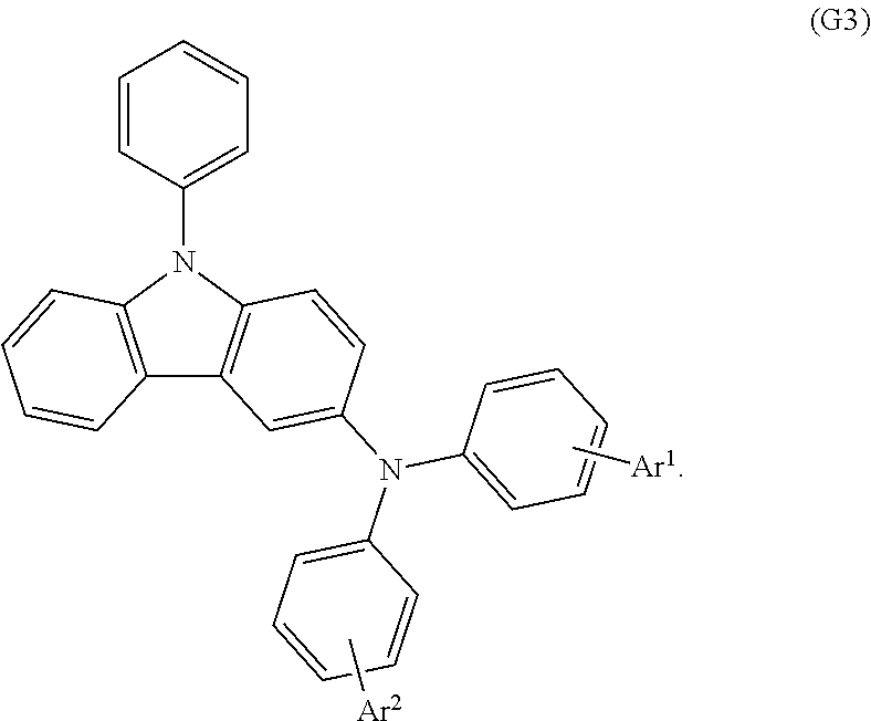
4. The light-emitting device according to claim 3 , wherein the organic compound is represented by a formula (G4)

5. The light-emitting device according to claim 4 , wherein the organic compound is represented by a formula (100)

6. The light-emitting device according to claim 4 , wherein the organic compound is represented by a formula (101)

7. The light-emitting device according to claim 1 , wherein the mass spectrometry is liquid chromatography mass spectrometry in a positive mode in which an argon gas is made to collide at any energy higher than or equal to 1 eV and lower than or equal to 30 eV with the organic compound.
8. An electronic device comprising the light-emitting device according to claim 1 .
9. A lighting device comprising the light-emitting device according to claim 1 .
10. A light-emitting device comprising:
an organic compound between a pair of electrodes; and
at least one of a hole-injection layer, a hole-transport layer, and a light-emitting layer,
wherein:
the organic compound is included in at least one of the hole-injection layer, the hole-transport layer and the light-emitting layer,
the organic compound comprises a phenylcarbazole skeleton and an N-biphenyl-N-phenylamine skeleton,
the N-biphenyl-N-phenylamine skeleton is bonded to a 3-position of the phenylcarbazole skeleton,
a molecular weight X of the organic compound is greater than or equal to 450 and less than or equal to 1500,
an absorption edge of the organic compound is at 380 nm or more, and
a product ion is detected at least around m/z=(X−240) by mass spectrometry.
11. The light-emitting device according to claim 10 , wherein the organic compound is represented by a formula (100)

12. The light-emitting device according to claim 10 , wherein the mass spectrometry is liquid chromatography mass spectrometry in a positive mode in which an argon gas is made to collide at any energy higher than or equal to 1 eV and lower than or equal to 30 eV with the organic compound.
13. An electronic device comprising the light-emitting device according to claim 10 .
14. A lighting device comprising the light-emitting device according to claim 10 .
15. A light-emitting device comprising:
an organic compound between a pair of electrodes; and
at least one of a hole-injection layer, a hole-transport layer, and a light-emitting layer,
wherein:
the organic compound is included in at least one of the hole-injection layer, the hole-transport layer and the light-emitting layer,
the organic compound comprises a phenylcarbazole skeleton and an N,N-bis-biphenylamine skeleton,
the N,N-bis-biphenylamine skeleton is bonded to a 3-position of the phenylcarbazole skeleton,
a molecular weight X of the organic compound is greater than or equal to 450 and less than or equal to 1500,
an absorption edge of the organic compound is at 380 nm or more, and
a product ion is detected at least around m/z=(X−240) by mass spectrometry.
16. The light-emitting device according to claim 15 , wherein the organic compound is represented by a formula (101)

17. The light-emitting device according to claim 15 , wherein the mass spectrometry is liquid chromatography mass spectrometry in a positive mode in which an argon gas is made to collide at any energy higher than or equal to 1 eV and lower than or equal to 30 eV with the organic compound.
18. An electronic device comprising the light-emitting device according to claim 15 .
19. A lighting device comprising the light-emitting device according to claim 15 .
Priority Applications (1)
| Application Number | Priority Date | Filing Date | Title |
|---|---|---|---|
| US15/696,776 US10629823B2 (en) | 2012-11-26 | 2017-09-06 | Light-emitting element, light-emitting device, electronic device, and lighting device |
Applications Claiming Priority (2)
| Application Number | Priority Date | Filing Date | Title |
|---|---|---|---|
| JP2012-257369 | 2012-11-26 | ||
| JP2012257369 | 2012-11-26 |
Related Child Applications (1)
| Application Number | Title | Priority Date | Filing Date |
|---|---|---|---|
| US15/696,776 Continuation US10629823B2 (en) | 2012-11-26 | 2017-09-06 | Light-emitting element, light-emitting device, electronic device, and lighting device |
Publications (2)
| Publication Number | Publication Date |
|---|---|
| US20140145166A1 US20140145166A1 (en) | 2014-05-29 |
| US9761812B2 true US9761812B2 (en) | 2017-09-12 |
Family
ID=50772459
Family Applications (2)
| Application Number | Title | Priority Date | Filing Date |
|---|---|---|---|
| US14/088,690 Active 2035-10-09 US9761812B2 (en) | 2012-11-26 | 2013-11-25 | Light-emitting element, light-emitting device, electronic device, and lighting device |
| US15/696,776 Active US10629823B2 (en) | 2012-11-26 | 2017-09-06 | Light-emitting element, light-emitting device, electronic device, and lighting device |
Family Applications After (1)
| Application Number | Title | Priority Date | Filing Date |
|---|---|---|---|
| US15/696,776 Active US10629823B2 (en) | 2012-11-26 | 2017-09-06 | Light-emitting element, light-emitting device, electronic device, and lighting device |
Country Status (4)
| Country | Link |
|---|---|
| US (2) | US9761812B2 (en) |
| JP (1) | JP2014123721A (en) |
| KR (3) | KR20140071897A (en) |
| CN (2) | CN103840084B (en) |
Cited By (1)
| Publication number | Priority date | Publication date | Assignee | Title |
|---|---|---|---|---|
| US11917882B2 (en) | 2014-08-08 | 2024-02-27 | Semiconductor Energy Laboratory Co., Ltd. | Light-emitting device, electronic device, and lighting device |
Families Citing this family (4)
| Publication number | Priority date | Publication date | Assignee | Title |
|---|---|---|---|---|
| KR102021273B1 (en) | 2011-05-27 | 2019-09-16 | 가부시키가이샤 한도오따이 에네루기 켄큐쇼 | Carbazole compound, light-emitting element, light-emitting device, electronic device, and lighting device |
| CN105810840B (en) * | 2014-12-29 | 2018-02-27 | 固安翌光科技有限公司 | A kind of organic electroluminescence device |
| CN105810839A (en) * | 2016-03-10 | 2016-07-27 | 南京邮电大学 | Monolayer blue light exciplex organic light-emitting device and manufacturing method thereof |
| CN109378392B (en) * | 2018-09-03 | 2020-12-08 | 云谷(固安)科技有限公司 | Organic electroluminescent device and display device |
Citations (40)
| Publication number | Priority date | Publication date | Assignee | Title |
|---|---|---|---|---|
| JPH02178670A (en) | 1988-12-29 | 1990-07-11 | Canon Inc | Electrophotographic sensitive body |
| JPH03118548A (en) | 1989-09-30 | 1991-05-21 | Ricoh Co Ltd | Method for recovering electrophotographic sensitive body from fatigue |
| JPH10310574A (en) | 1997-05-09 | 1998-11-24 | Minolta Co Ltd | Novel amino compound, its production and use |
| WO2006070907A1 (en) | 2004-12-28 | 2006-07-06 | Semiconductor Energy Laboratory Co., Ltd. | Anthracene derivative, light emitting element using the same, and light emitting device using the same |
| US20070075632A1 (en) | 2005-09-02 | 2007-04-05 | Semiconductor Energy Laboratory Co., Ltd. | Anthracene derivative |
| WO2007043484A1 (en) | 2005-10-07 | 2007-04-19 | Toyo Ink Manufacturing Co., Ltd. | Carbazole-containing amine compound and use thereof |
| US20070231503A1 (en) | 2004-04-02 | 2007-10-04 | Hwang Seok-Hwan | Organic light emitting device and flat panel display device comprising the same |
| WO2008010377A1 (en) | 2006-07-21 | 2008-01-24 | Toyo Ink Manufacturing Co., Ltd. | Carbazole-containing amine compound and use thereof |
| US20080099757A1 (en) | 2006-01-26 | 2008-05-01 | Shinobu Furukawa | Organic field effect transistor and semiconductor device |
| US20080107919A1 (en) | 2004-11-29 | 2008-05-08 | Seok-Hwan Hwang | Phenylcarbazole-based compound and organic electroluminescent device employing the same |
| US20080106188A1 (en) | 2006-11-08 | 2008-05-08 | Seok-Hwan Hwang | Silanylamine-based compound, method of preparing the same and organic light emitting device including organic layer comprising the silanylamine-based compound |
| US20080254318A1 (en) | 2004-12-28 | 2008-10-16 | Semiconductor Energy Laboratory Co., Ltd. | Carbazole Derivative, and Light-Emitting Element and Light-Emitting Device Using the Carbzole Derivative |
| US20080284328A1 (en) | 2004-10-19 | 2008-11-20 | Semiconductor Energy Laboratory, Ltd. | Carbazole Derivative, and Light Emitting Element and Light Emitting Device Using the Carbazole Derivative |
| US20090015140A1 (en) | 2005-03-28 | 2009-01-15 | Semiconductor Energy Laboratory Co., Ltd. | Anthracene Derivative, Material for Light Emitting Element, Light Emitting Element, Light Emitting Device, and Electronic Device |
| US20090058267A1 (en) | 2004-11-30 | 2009-03-05 | Semiconductor Energy Laboratory Co., Ltd. | Light emitting element and light emitting device |
| US20090206745A1 (en) | 2008-02-18 | 2009-08-20 | Seok-Hwan Hwang | Silanylamine-based compound and organic light emitting diode |
| WO2010021524A2 (en) | 2008-08-22 | 2010-02-25 | 주식회사 엘지화학 | Material for organic electronic device, and organic electronic device using the same |
| US20100069647A1 (en) | 2008-07-08 | 2010-03-18 | Semiconductor Energy Laboratory Co., Ltd. | Carbazole Derivative, Light-Emitting Element Material, Light-Emitting Element, and Light-Emitting Device |
| WO2010067746A1 (en) | 2008-12-08 | 2010-06-17 | コニカミノルタホールディングス株式会社 | Organic electroluminescence element, display device and illumination device |
| US20100207517A1 (en) | 2009-02-19 | 2010-08-19 | Semiconductor Energy Laboratory Co., Ltd. | Oxadiazole Derivative, and Light-Emitting Element and Light-Emitting Device Using Oxadiazole Derivative |
| WO2010113743A1 (en) | 2009-03-30 | 2010-10-07 | 東レ株式会社 | Light-emitting element material and light-emitting element |
| KR20100123172A (en) | 2009-05-14 | 2010-11-24 | 덕산하이메탈(주) | Chemical comprising arylamino and organic electronic element using the same, terminal thererof |
| KR20100132109A (en) | 2009-06-09 | 2010-12-17 | 주식회사 이엘엠 | Organic light emitting material and organic light emitting diode having the same |
| JP2011001349A (en) * | 2009-05-20 | 2011-01-06 | Tosoh Corp | 2-aminocarbazole compound and application thereof |
| KR101007516B1 (en) | 2010-04-23 | 2011-01-14 | 주식회사 이엘엠 | Organic light emitting material and organic light emitting diode having the same |
| US20110049487A1 (en) | 2009-08-28 | 2011-03-03 | Young-Kook Kim | Heteroarylamine compound and organic luminescence device using the same |
| WO2011031086A2 (en) | 2009-09-10 | 2011-03-17 | 주식회사 엘지화학 | New heterocyclic derivative and organic light emitting device using same |
| JP4729641B1 (en) | 2010-07-05 | 2011-07-20 | 富士フイルム株式会社 | Organic electroluminescence device |
| WO2011090149A1 (en) | 2010-01-21 | 2011-07-28 | 出光興産株式会社 | Aromatic amine derivative, and organic electroluminescent element comprising same |
| KR20110087768A (en) | 2010-01-27 | 2011-08-03 | 덕산하이메탈(주) | Aromatic amine compund and organic electroric element using the same, terminal thererof |
| KR20110111967A (en) | 2010-04-06 | 2011-10-12 | 덕산하이메탈(주) | Chemical comprising naphthylcarbazole derivatives and organic electronic element using the same, terminal thereof |
| KR20110134581A (en) | 2010-06-09 | 2011-12-15 | 다우어드밴스드디스플레이머티리얼 유한회사 | Novel organic electroluminescent compounds and organic electroluminescent device using the same |
| WO2012005360A1 (en) | 2010-07-09 | 2012-01-12 | 富士フイルム株式会社 | Organic electroluminescent element |
| US20120007495A1 (en) | 2010-07-07 | 2012-01-12 | Samsung Mobile Display Co., Ltd. | Organic material and organic light emitting device including the same |
| US20120012824A1 (en) | 2010-07-14 | 2012-01-19 | Samsung Mobile Display Co., Ltd. | Metal complex compound and organic light emitting diode device including the same |
| KR20120009761A (en) | 2010-07-21 | 2012-02-02 | 롬엔드하스전자재료코리아유한회사 | Novel organic electroluminescent compounds and organic electroluminescent device using the same |
| US20120071668A1 (en) | 2010-09-21 | 2012-03-22 | Semiconductor Energy Laboratory Co., Ltd. | Carbazole Derivative, Light-Emitting Element Material and Organic Semiconductor Material |
| US20120077987A1 (en) | 2010-09-27 | 2012-03-29 | Semiconductor Energy Laboratory Co., Ltd. | Organic compound, light-emitting element, light-emitting device, electronic device, and lighting device |
| KR20120039470A (en) | 2010-10-15 | 2012-04-25 | 제이엔씨 주식회사 | Emission layer material and organic electroluminescence element using the same |
| US20120302762A1 (en) | 2011-05-27 | 2012-11-29 | Semiconductor Energy Laboratory Co., Ltd. | Carbazole Compound, Light-Emitting Element, Light-Emitting Device, Electronic Device, and Lighting Device |
Family Cites Families (13)
| Publication number | Priority date | Publication date | Assignee | Title |
|---|---|---|---|---|
| JPS4729641Y1 (en) | 1969-10-15 | 1972-09-05 | ||
| JP4243237B2 (en) * | 2003-11-10 | 2009-03-25 | 淳二 城戸 | Organic element, organic EL element, organic solar cell, organic FET structure, and organic element manufacturing method |
| KR100846586B1 (en) | 2006-05-29 | 2008-07-16 | 삼성에스디아이 주식회사 | An organic light emitting device and a flat panel display device comprising the same |
| KR100669716B1 (en) | 2004-07-14 | 2007-01-16 | 삼성에스디아이 주식회사 | Phenylcarbazole compounds and organic electroluminescence devices using the same |
| KR100573137B1 (en) * | 2004-04-02 | 2006-04-24 | 삼성에스디아이 주식회사 | Fluorene-based compound and organic electroluminescent display device using the same |
| KR100787425B1 (en) | 2004-11-29 | 2007-12-26 | 삼성에스디아이 주식회사 | Phenylcarbazole-based compound and Organic electroluminescence display employing the same |
| EP1866983A4 (en) * | 2005-02-28 | 2009-10-21 | Semiconductor Energy Lab | Composite material, light emitting element, light emitting device and electronic appliance using the composite material |
| US7728517B2 (en) * | 2005-05-20 | 2010-06-01 | Lg Display Co., Ltd. | Intermediate electrodes for stacked OLEDs |
| JP5082356B2 (en) * | 2005-10-07 | 2012-11-28 | 東洋インキScホールディングス株式会社 | Carbazole-containing amine compounds and uses thereof |
| KR102022839B1 (en) | 2007-12-03 | 2019-09-20 | 가부시키가이샤 한도오따이 에네루기 켄큐쇼 | Carbazole derivative, and light-emitting element, light-emitting device, and electronic device using carbazole derivative |
| CN101609871A (en) * | 2008-06-18 | 2009-12-23 | 中国科学院半导体研究所 | Organic electroluminescence device and preparation method thereof |
| US9450192B2 (en) * | 2010-12-06 | 2016-09-20 | E-Ray Optoelectronics Technology | Carbazole derivative and organic electroluminescent devices utilizing the same and fabrication method thereof |
| KR101298483B1 (en) * | 2011-04-01 | 2013-08-21 | 덕산하이메탈(주) | Chemical and Organic Electronic Element using the same, Electronic Device thereof |
-
2013
- 2013-11-20 KR KR1020130141726A patent/KR20140071897A/en active Application Filing
- 2013-11-22 JP JP2013242068A patent/JP2014123721A/en not_active Withdrawn
- 2013-11-25 CN CN201310606271.7A patent/CN103840084B/en active Active
- 2013-11-25 US US14/088,690 patent/US9761812B2/en active Active
- 2013-11-25 CN CN201711116364.6A patent/CN107623088B/en active Active
-
2017
- 2017-09-06 US US15/696,776 patent/US10629823B2/en active Active
-
2021
- 2021-04-19 KR KR1020210050488A patent/KR102437255B1/en active IP Right Grant
-
2022
- 2022-08-23 KR KR1020220105542A patent/KR20220122953A/en not_active Application Discontinuation
Patent Citations (44)
| Publication number | Priority date | Publication date | Assignee | Title |
|---|---|---|---|---|
| US5049464A (en) | 1988-12-29 | 1991-09-17 | Canon Kabushiki Kaisha | Photosensitive member for electrophotography |
| JPH02178670A (en) | 1988-12-29 | 1990-07-11 | Canon Inc | Electrophotographic sensitive body |
| JPH03118548A (en) | 1989-09-30 | 1991-05-21 | Ricoh Co Ltd | Method for recovering electrophotographic sensitive body from fatigue |
| JPH10310574A (en) | 1997-05-09 | 1998-11-24 | Minolta Co Ltd | Novel amino compound, its production and use |
| US20070231503A1 (en) | 2004-04-02 | 2007-10-04 | Hwang Seok-Hwan | Organic light emitting device and flat panel display device comprising the same |
| US20080284328A1 (en) | 2004-10-19 | 2008-11-20 | Semiconductor Energy Laboratory, Ltd. | Carbazole Derivative, and Light Emitting Element and Light Emitting Device Using the Carbazole Derivative |
| US20080107919A1 (en) | 2004-11-29 | 2008-05-08 | Seok-Hwan Hwang | Phenylcarbazole-based compound and organic electroluminescent device employing the same |
| US20090058267A1 (en) | 2004-11-30 | 2009-03-05 | Semiconductor Energy Laboratory Co., Ltd. | Light emitting element and light emitting device |
| WO2006070907A1 (en) | 2004-12-28 | 2006-07-06 | Semiconductor Energy Laboratory Co., Ltd. | Anthracene derivative, light emitting element using the same, and light emitting device using the same |
| US20080254318A1 (en) | 2004-12-28 | 2008-10-16 | Semiconductor Energy Laboratory Co., Ltd. | Carbazole Derivative, and Light-Emitting Element and Light-Emitting Device Using the Carbzole Derivative |
| US20090015140A1 (en) | 2005-03-28 | 2009-01-15 | Semiconductor Energy Laboratory Co., Ltd. | Anthracene Derivative, Material for Light Emitting Element, Light Emitting Element, Light Emitting Device, and Electronic Device |
| US20070075632A1 (en) | 2005-09-02 | 2007-04-05 | Semiconductor Energy Laboratory Co., Ltd. | Anthracene derivative |
| WO2007043484A1 (en) | 2005-10-07 | 2007-04-19 | Toyo Ink Manufacturing Co., Ltd. | Carbazole-containing amine compound and use thereof |
| US20080099757A1 (en) | 2006-01-26 | 2008-05-01 | Shinobu Furukawa | Organic field effect transistor and semiconductor device |
| WO2008010377A1 (en) | 2006-07-21 | 2008-01-24 | Toyo Ink Manufacturing Co., Ltd. | Carbazole-containing amine compound and use thereof |
| US20080106188A1 (en) | 2006-11-08 | 2008-05-08 | Seok-Hwan Hwang | Silanylamine-based compound, method of preparing the same and organic light emitting device including organic layer comprising the silanylamine-based compound |
| US20090206745A1 (en) | 2008-02-18 | 2009-08-20 | Seok-Hwan Hwang | Silanylamine-based compound and organic light emitting diode |
| US20100069647A1 (en) | 2008-07-08 | 2010-03-18 | Semiconductor Energy Laboratory Co., Ltd. | Carbazole Derivative, Light-Emitting Element Material, Light-Emitting Element, and Light-Emitting Device |
| WO2010021524A2 (en) | 2008-08-22 | 2010-02-25 | 주식회사 엘지화학 | Material for organic electronic device, and organic electronic device using the same |
| WO2010067746A1 (en) | 2008-12-08 | 2010-06-17 | コニカミノルタホールディングス株式会社 | Organic electroluminescence element, display device and illumination device |
| US20100207517A1 (en) | 2009-02-19 | 2010-08-19 | Semiconductor Energy Laboratory Co., Ltd. | Oxadiazole Derivative, and Light-Emitting Element and Light-Emitting Device Using Oxadiazole Derivative |
| CN101812057A (en) | 2009-02-19 | 2010-08-25 | 株式会社半导体能源研究所 | The luminous element and the light-emitting device of oxadiazole derivative, Shi Yong oxadiazole derivative |
| WO2010113743A1 (en) | 2009-03-30 | 2010-10-07 | 東レ株式会社 | Light-emitting element material and light-emitting element |
| KR20100123172A (en) | 2009-05-14 | 2010-11-24 | 덕산하이메탈(주) | Chemical comprising arylamino and organic electronic element using the same, terminal thererof |
| KR101070223B1 (en) | 2009-05-14 | 2011-10-06 | 덕산하이메탈(주) | Chemical comprising arylamino and organic electronic element using the same, terminal thererof |
| JP2011001349A (en) * | 2009-05-20 | 2011-01-06 | Tosoh Corp | 2-aminocarbazole compound and application thereof |
| KR20100132109A (en) | 2009-06-09 | 2010-12-17 | 주식회사 이엘엠 | Organic light emitting material and organic light emitting diode having the same |
| US20110049487A1 (en) | 2009-08-28 | 2011-03-03 | Young-Kook Kim | Heteroarylamine compound and organic luminescence device using the same |
| WO2011031086A2 (en) | 2009-09-10 | 2011-03-17 | 주식회사 엘지화학 | New heterocyclic derivative and organic light emitting device using same |
| WO2011090149A1 (en) | 2010-01-21 | 2011-07-28 | 出光興産株式会社 | Aromatic amine derivative, and organic electroluminescent element comprising same |
| KR20110087768A (en) | 2010-01-27 | 2011-08-03 | 덕산하이메탈(주) | Aromatic amine compund and organic electroric element using the same, terminal thererof |
| KR20110111967A (en) | 2010-04-06 | 2011-10-12 | 덕산하이메탈(주) | Chemical comprising naphthylcarbazole derivatives and organic electronic element using the same, terminal thereof |
| KR101007516B1 (en) | 2010-04-23 | 2011-01-14 | 주식회사 이엘엠 | Organic light emitting material and organic light emitting diode having the same |
| KR20110134581A (en) | 2010-06-09 | 2011-12-15 | 다우어드밴스드디스플레이머티리얼 유한회사 | Novel organic electroluminescent compounds and organic electroluminescent device using the same |
| JP4729641B1 (en) | 2010-07-05 | 2011-07-20 | 富士フイルム株式会社 | Organic electroluminescence device |
| US20120007495A1 (en) | 2010-07-07 | 2012-01-12 | Samsung Mobile Display Co., Ltd. | Organic material and organic light emitting device including the same |
| WO2012005360A1 (en) | 2010-07-09 | 2012-01-12 | 富士フイルム株式会社 | Organic electroluminescent element |
| US20120012824A1 (en) | 2010-07-14 | 2012-01-19 | Samsung Mobile Display Co., Ltd. | Metal complex compound and organic light emitting diode device including the same |
| KR20120009761A (en) | 2010-07-21 | 2012-02-02 | 롬엔드하스전자재료코리아유한회사 | Novel organic electroluminescent compounds and organic electroluminescent device using the same |
| US20120071668A1 (en) | 2010-09-21 | 2012-03-22 | Semiconductor Energy Laboratory Co., Ltd. | Carbazole Derivative, Light-Emitting Element Material and Organic Semiconductor Material |
| US20120077987A1 (en) | 2010-09-27 | 2012-03-29 | Semiconductor Energy Laboratory Co., Ltd. | Organic compound, light-emitting element, light-emitting device, electronic device, and lighting device |
| KR20120039470A (en) | 2010-10-15 | 2012-04-25 | 제이엔씨 주식회사 | Emission layer material and organic electroluminescence element using the same |
| US20120302762A1 (en) | 2011-05-27 | 2012-11-29 | Semiconductor Energy Laboratory Co., Ltd. | Carbazole Compound, Light-Emitting Element, Light-Emitting Device, Electronic Device, and Lighting Device |
| JP2013010749A (en) | 2011-05-27 | 2013-01-17 | Semiconductor Energy Lab Co Ltd | Carbazole compound, light-emitting element, light-emitting device, electronic device and lighting system |
Non-Patent Citations (6)
| Title |
|---|
| Balionyte, A. et al., "Polymers Containing 9-alkylcarbazol-3,6-diyl and Different Aromatic Amino Groups in the Main Chain," Europian Polymer Journal , Aug. 1, 2005, vol. 41, No. 8, pp. 1821-1827. |
| Chinese Office Action re Application No. CN 201310606271.7, dated Aug. 29, 2016. |
| Final Rejection re U.S. Appl. No. 13/481,142, dated Sep. 24, 2013. |
| Ho, M.-H. et al., "P-131: Novel Deep Blue Dopants for Organic Light-Emitting Devices," SID Digest '05: SID International Symposium Digest of Technical Papers, vol. 36, May 24, 2005, pp. 802-805. |
| Office Action re U.S. Appl. No. 13/481,142, dated Apr. 15, 2014. |
| Office Action re U.S. Appl. No. 13/481,142, dated Apr. 24, 2013. |
Cited By (1)
| Publication number | Priority date | Publication date | Assignee | Title |
|---|---|---|---|---|
| US11917882B2 (en) | 2014-08-08 | 2024-02-27 | Semiconductor Energy Laboratory Co., Ltd. | Light-emitting device, electronic device, and lighting device |
Also Published As
| Publication number | Publication date |
|---|---|
| US20140145166A1 (en) | 2014-05-29 |
| CN107623088B (en) | 2020-01-10 |
| KR20210049734A (en) | 2021-05-06 |
| KR102437255B1 (en) | 2022-08-26 |
| KR20220122953A (en) | 2022-09-05 |
| US20170365797A1 (en) | 2017-12-21 |
| CN107623088A (en) | 2018-01-23 |
| CN103840084B (en) | 2017-12-15 |
| US10629823B2 (en) | 2020-04-21 |
| JP2014123721A (en) | 2014-07-03 |
| CN103840084A (en) | 2014-06-04 |
| KR20140071897A (en) | 2014-06-12 |
Similar Documents
| Publication | Publication Date | Title |
|---|---|---|
| KR102208019B1 (en) | Carbazole compound, light-emitting element, light-emitting device, electronic device, and lighting device | |
| KR102388405B1 (en) | Triarylamine compound, light-emitting element, light-emitting device, electronic device, and lighting device | |
| US9899603B2 (en) | Organic compound, light-emitting element, light-emitting device, electronic appliance, and lighting device | |
| US10665791B2 (en) | Heterocyclic compound, light-emitting element, light-emitting device, electronic device, and lighting device | |
| US9130182B2 (en) | Light-emitting element, lighting device, light-emitting device, and electronic device | |
| US20210013421A1 (en) | Heterocyclic Compound, Light-Emitting Element, Light-Emitting Device, Electronic Device, and Lighting Device | |
| US9960369B2 (en) | Compound, light-emitting element, light-emitting device, electronic device, and lighting device | |
| US10629823B2 (en) | Light-emitting element, light-emitting device, electronic device, and lighting device | |
| CN105732588B (en) | Organic compound, light-emitting element, and light-emitting device | |
| JP7157229B2 (en) | Light-emitting elements, light-emitting devices, electronic devices and lighting devices | |
| US20160075718A1 (en) | Organic Compound, Light-Emitting Element, Light-Emitting Device, Electronic Device, and Lighting Device | |
| JP6002503B2 (en) | Carbazole compounds |
Legal Events
| Date | Code | Title | Description |
|---|---|---|---|
| AS | Assignment |
Owner name: SEMICONDUCTOR ENERGY LABORATORY CO., LTD., JAPAN Free format text: ASSIGNMENT OF ASSIGNORS INTEREST;ASSIGNORS:OSAKA, HARUE;SHITAGAKI, SATOKO;OHSAWA, NOBUHARU;SIGNING DATES FROM 20131114 TO 20131120;REEL/FRAME:031667/0596 |
|
| STCF | Information on status: patent grant |
Free format text: PATENTED CASE |
|
| MAFP | Maintenance fee payment |
Free format text: PAYMENT OF MAINTENANCE FEE, 4TH YEAR, LARGE ENTITY (ORIGINAL EVENT CODE: M1551); ENTITY STATUS OF PATENT OWNER: LARGE ENTITY Year of fee payment: 4 |