US9720037B2 - Debug circuit, semiconductor device, and debug method - Google Patents
Debug circuit, semiconductor device, and debug method Download PDFInfo
- Publication number
- US9720037B2 US9720037B2 US15/085,298 US201615085298A US9720037B2 US 9720037 B2 US9720037 B2 US 9720037B2 US 201615085298 A US201615085298 A US 201615085298A US 9720037 B2 US9720037 B2 US 9720037B2
- Authority
- US
- United States
- Prior art keywords
- sequence
- code value
- value
- circuit
- code
- Prior art date
- Legal status (The legal status is an assumption and is not a legal conclusion. Google has not performed a legal analysis and makes no representation as to the accuracy of the status listed.)
- Active
Links
Images


Classifications
-
- G—PHYSICS
- G01—MEASURING; TESTING
- G01R—MEASURING ELECTRIC VARIABLES; MEASURING MAGNETIC VARIABLES
- G01R31/00—Arrangements for testing electric properties; Arrangements for locating electric faults; Arrangements for electrical testing characterised by what is being tested not provided for elsewhere
- G01R31/28—Testing of electronic circuits, e.g. by signal tracer
- G01R31/317—Testing of digital circuits
- G01R31/31705—Debugging aspects, e.g. using test circuits for debugging, using dedicated debugging test circuits
-
- G—PHYSICS
- G01—MEASURING; TESTING
- G01R—MEASURING ELECTRIC VARIABLES; MEASURING MAGNETIC VARIABLES
- G01R31/00—Arrangements for testing electric properties; Arrangements for locating electric faults; Arrangements for electrical testing characterised by what is being tested not provided for elsewhere
- G01R31/28—Testing of electronic circuits, e.g. by signal tracer
- G01R31/317—Testing of digital circuits
- G01R31/3177—Testing of logic operation, e.g. by logic analysers
Definitions
- the embodiments discussed herein relate to a debug circuit, a semiconductor device, and a debug method.
- One of actual-hardware debugging systems for checking whether or not actual hardware normally operates is a logic analyzer in which a debug circuit is inserted at mounting of a debug-target circuit, and performs debugging.
- the debug circuit monitors a signal sequence (signal transition) of the debug-target circuit designated by the user. Then, when the signal sequence matches a predetermined stop condition, the debug circuit stops operation of the circuit, and outputs the signal sequence stored in a trace memory to a display or the like.
- a debug circuit includes a memory configured to store, among code values calculated in accordance with a coding scheme that varies code values according to a signal sequence in a debug-target circuit, a first code value obtained by coding a leading first sequence of a plurality of sequences divided from a detection-target sequence detected from the signal sequence, a second code value obtained by coding a third sequence being a designated value sequence in each of two or more second sequences of the plurality of sequences, and a length of a fourth sequence being a don't-care value sequence in each of the second sequences; a code value calculation circuit configured to calculate third code values by coding the signal sequence in accordance with the coding scheme; a first sequence detection circuit configured to detect the first sequence based on comparison of the first code value with a difference between the current third code value and a fourth code value that is the third code value preceding the current third code value by a length of the first sequence; an expected value calculation circuit configured to calculate an expected value of the third code value
- FIG. 1A is a view illustrating an example of a semiconductor device, a debug circuit, and a debugger device in First embodiment
- FIG. 1B is a view illustrating an example of a detection-target sequence S
- FIG. 1C is a view illustrating an example of updating of a code value of the detection-target sequence
- FIG. 2 is a view illustrating an example of a debug system including a semiconductor device and a debugger device in Second embodiment
- FIG. 3 is a view illustrating an example of the semiconductor device
- FIG. 4 is a view illustrating an example of storage of information in registers
- FIG. 5 is a view illustrating an example of storage of information in a register
- FIG. 6 is a view illustrating an example of a match determination circuit
- FIG. 7 is a view illustrating an example of a partial sequence end determination circuit
- FIG. 8 is a view illustrating an example of a final sequence determination circuit
- FIG. 9 is a view illustrating an example of hardware of a debugger device
- FIG. 10 is a flow chart illustrating an example of setting processing of the debugger device
- FIG. 11 is a flow chart illustrating an example of processing of the semiconductor device
- FIG. 12 is a view illustrating an example of detection of a sequence Sa
- FIG. 13 is a view illustrating an example of calculation of an expected value
- FIG. 14 is a view illustrating sequence end determination processing
- FIG. 15 is a view illustrating an example of transition of input data.
- FIG. 16 is a view illustrating an example of detection results and end determination results of each sequence in detection-target sequence detection processing.
- FIG. 1A is a view illustrating an example of a semiconductor device, debug circuit, and a debugger device in First embodiment.
- a semiconductor device 1 includes a debug circuit 2 and a debug-target circuit 3 .
- the debug-target circuit 3 is, for example, hardware that transmits and receives data, and performs calculation.
- the debug circuit 2 detects a predetermined signal sequence (hereinafter referred to a detection-target sequence), which serves as a stop condition of the debug-target circuit 3 , from any signal sequence in the debug-target circuit 3 , and outputs a detection signal indicating that the detection-target sequence is detected.
- the detection signal is used to stop operation of the debug-target circuit 3 , for example.
- the detection-target sequence may include a designated value and a don't-care value that does not affect a detection result of the detection-target sequence.
- the don't-care value may be any value.
- the don't-care value is set for a value that is unknown at debugging or the like.
- Information on a length of a sequence including such don't-care values (hereinafter, also referred to as a don't-care value sequence) is provided from, for example, a debugger device 4 .
- the debug circuit 2 in this embodiment may set the signal sequence including such don't-care value as a detection target.
- FIG. 1B illustrates an example of a detection-target sequence S.
- a plurality of elliptical elements each denote the designated value or the don't-care value.
- the detection-target sequence S is divided into three sequences Sa, Sb 1 , and Sb 2 , and the second sequence Sb 1 includes a designated value sequence having a length L 1 , and a don't-care value sequence having a length L 2 .
- the leading sequence Sa and the tailing sequence Sb 2 do not include the don't-care value.
- the lengths L 1 , L 2 of the sequences are expressed as the number of bytes, for example.
- the detection-target sequence S may be divided into four or more sequences.
- the debug circuit 2 has a memory 2 a , a code value calculation circuit 2 b , a delay circuit 2 c , a first sequence detection circuit 2 d , an expected value calculation circuit 2 e , and a determination circuit 2 f .
- the memory 2 a may include a volatile storage medium and a nonvolatile storage medium. Examples of the volatile storage medium include a random access memory (RAM).
- the nonvolatile storage medium may include at least one of a hard disc drive (HDD), a solid state drive (SSD), an electrically erasable programmable read-only memory (EEPROM), and a flash memory.
- the debug circuit 2 further includes a counter 2 g that counts the number of data (e.g. the number of bytes) of input data x input to the debug-target circuit 3 and output data y output from the debug-target circuit 3 .
- the memory 2 a stores a code value Aa obtained by coding the sequence Sa, code values Ab 1 , Ab 2 obtained by coding designated value sequences in the sequences Sb 1 , Sb 2 , and the length L 2 of a don't-care value sequence.
- the memory 2 a may further store lengths of the designated value sequences Sa, Sb 1 , and Sb 2 , and identification information of the detection-target sequence S.
- the code values Aa, Ab 1 , and Ab 2 are calculated in accordance with a coding scheme that varies the code value according to the signal sequence in the debug-target circuit 3 .
- the code values Aa, Ab 1 , and Ab 2 are, for example, code values (linear codes) having linearity, and are calculated by the debugger device 4 in accordance with a coding scheme such as Cyclic Redundancy Check (CRC).
- CRC Cyclic Redundancy Check
- the code value calculation circuit 2 b calculates the code value according to the signal sequence of the debug-target circuit 3 , in accordance with the same coding scheme as the coding scheme used when the debugger device 4 calculates the code values Aa, Ab 1 , and Ab 2 .
- the code value calculation circuit 2 b acquires the signal of the debug-target circuit 3 (input data x or output data y) in units of bytes, and updates the code value.
- the detection-target sequence S is a sequence in units of bytes.
- FIG. 1C illustrates an example of the code value calculated when the input data x or the output data y as the signal of the debug-target circuit 3 transitions from a state of D(i) to states D(j) and then, D(j+L 1 ).
- the state of D(i) have to not be an initial state, and may be a state in the middle of a certain sequence.
- i, j, and j+L 1 each denote a count value of the counter 2 g .
- the length L 1 of the designated value sequence in the sequence Sb 1 is expressed as the number of bytes (the number of counts).
- the delay circuit 2 c outputs a code value that is calculated by the code value calculation circuit 2 b at an earlier time by a period corresponding to a length of the sequence Sa in the detection-target sequence S.
- the delay circuit 2 c is a shift register, and holds each of the code values calculated by the code value calculation circuit 2 b for the length of the sequence Sa, and outputs the code values one after another from the firstly input code value. That is, the delay circuit 2 c functions of delaying outputting of the input code values.
- FIG. 1A illustrates the example in which the delay circuit 2 c outputs a code value a(j ⁇ m).
- the code value a(j ⁇ m) is a code value preceding from a code value a(j) by m counts.
- the first sequence detection circuit 2 d compares a difference between the code value output from the code value calculation circuit 2 b and the code value output from the delay circuit 2 c with the code value Aa, and detects the leading sequence Sa in the plurality of sequences divided from the detection-target sequence S based on the comparison. That is, the first sequence detection circuit 2 d detects the sequence Sa based on comparison between the change in the code values of m counts and the code value Aa.
- the first sequence detection circuit 2 d detects that the signal of the debug-target circuit 3 transitions in the sequence Sa.
- FIG. 1C illustrates a detection example in which the sequence Sa follows an unknown sequence X.
- the sequence Sa is detected.
- the first sequence detection circuit 2 d When detecting the sequence Sa, the first sequence detection circuit 2 d supplies the code value output from the code value calculation circuit 2 b at detection to the expected value calculation circuit 2 e .
- the code value a(j) is supplied to the expected value calculation circuit 2 e.
- the expected value calculation circuit 2 e calculates an expected value of the code value calculated by the code value calculation circuit 2 b at the end of the designated value sequence in the sequence Sb 1 based on the code value output at detection of the sequence Sa among the code values calculated by the code value calculation circuit 2 b , and a code value Ab 1 .
- the expected value calculation circuit 2 e calculates an expected value of the code value calculated by the code value calculation circuit 2 b at the end of the designated value sequence in the sequence Sb 2 based on the code value output at detection of the sequence Sb 1 among the code values calculated by the code value calculation circuit 2 b , and a code value Ab 2 .
- the expected value calculation circuit 2 e calculated an expected value b(j+L 1 ) according to an XOR of the code value a(j) and the code value Ab 1 .
- An example of an expression of calculating the expected value will be described later (refer to expression (3)).
- the determination circuit 2 f detects the end of the sequences Sb 1 , Sb 2 based on the length of the don't-care value sequence, and notifies the detection to the expected value calculation circuit 2 e.
- the sequence Sb 1 includes the don't-care values, and the length of the don't-care value sequence is L 2 .
- the determination circuit 2 f determines the end of the sequence Sb 1 .
- the sequence Sb 2 does not include the don't-care value and thus, the length of the don't-care value sequence is 0. Accordingly, when the count value becomes a value at a time when the code value output from the code value calculation circuit 2 b matches the expected value, the determination circuit 2 f determines the end of the sequence Sb 2 .
- the determination circuit 2 f When detecting the end of all the sequences Sb 1 , Sb 2 , the determination circuit 2 f outputs a signal indicating detection of the detection-target sequence.
- the determination circuit 2 f includes a match determination circuit 2 f 1 , a partial sequence end determination circuit 2 f 2 , and a final sequence determination circuit 2 f 3 .
- the match determination circuit 2 f 1 determines whether or not the expected value calculated by the expected value calculation circuit 2 e matches the code value calculated by the code value calculation circuit 2 b .
- the partial sequence end determination circuit 2 f 2 acquires the length of the don't-care value sequence from the memory 2 a , and determines whether or not the sequences Sb 1 , Sb 2 end based on the length. For example, when the count value in the counter 2 g increases from the count value at a time when the match determination circuit 2 f 1 detects matching between the code value and the expected value, by a count number corresponding to the length of the don't-care value sequence, the partial sequence end determination circuit 2 f 2 determines that the sequences Sb 1 , Sb 2 end. In the above-mentioned example, when the count value is (j+L 1 +L 2 ), the end of the sequence Sb 1 is determined.
- the partial sequence end determination circuit 2 f 2 When determining the end of the sequences Sb 1 , Sb 2 , the partial sequence end determination circuit 2 f 2 notifies the expected value calculation circuit 2 e and the final sequence determination circuit 2 f 3 of the detection of the sequences Sb 1 , Sb 2 .
- the final sequence determination circuit 2 f 3 detects the number of sequences divided from the detection-target sequence S, from information stored in the memory 2 a .
- the number of divided sequences itself may be stored in the memory 2 a , and in this case, the final sequence determination circuit 2 f 3 may acquire the number of sequences thus stored. Then, based on the number of sequences, the final sequence determination circuit 2 f 3 determines whether or not the end of all the sequences Sb 1 , Sb 2 is notified by the partial sequence end determination circuit 2 f 2 .
- the final sequence determination circuit 2 f 3 outputs a signal indicating detection of the detection-target sequence. This signal serves as a circuit stop signal that instructs stop of operation of the debug-target circuit 3 .
- the final sequence determination circuit 2 f 3 stops supply of a clock signal to the debug-target circuit 3 in response to the circuit stop signal, thereby stopping operation of the debug-target circuit 3 .
- the final sequence determination circuit 2 f 3 may block inputting of data to the debug-target circuit 3 or outputting data from the debug-target circuit 3 to stop the debug-target circuit 3 .
- the debugger device 4 illustrated in FIG. 1A communicates with the semiconductor device 1 to perform debugging.
- the debugger device 4 is, for example, a computer, and executes following processing using software.
- the debugger device 4 first acquires the detection-target sequence S from a user (debug operator) (Step S 1 ).
- the debugger device 4 divides the detection-target sequence S into the sequences Sa, Sb 1 , and Sb 2 as illustrated in FIG. 1B (Step S 2 ).
- the debugger device 4 calculates the code values Aa, Ab 1 , and Ab 2 obtained by coding the designated value sequences in the sequences Sa, Sb 1 , and Sb 2 , respectively (Step S 3 ).
- the debugger device 4 outputs (transmits) information on the sequences Sa, Sb 1 , and Sb 2 , which includes the calculated code values Aa, Ab 1 , and Ab 2 and the length L 2 of the don't-care value sequence, to the semiconductor device 1 (Step S 4 ).
- the debug circuit 2 detects transition of the signal of the debug-target circuit 3 , and in the example illustrate in FIG. 1A , the code value calculation circuit 2 b updates the code value based on the sequence of the input data x or the output data y.
- the output of the code value calculation circuit 2 b is updated from the code value a(i) to a(j), and a(j+L 1 ).
- the first sequence detection circuit 2 d supplies the code value a(j) to the expected value calculation circuit 2 e .
- the expected value calculation circuit 2 e calculates the expected value b(j+L 1 ) based on the code value a(j) and the code value Ab 1 .
- the partial sequence end determination circuit 2 f 2 detects the end of the sequence Sb 1 when the count value is (j+L 1 +L 2 ).
- the expected value calculation circuit 2 e calculates the expected value at the end of the sequence Sb 2 in the same manner based on the code value a(j+L 1 +L 2 ) and the code value Ab 2 .
- the match determination circuit 2 f 1 detects matching between the expected value and the code value output from the code value calculation circuit 2 b
- the partial sequence end determination circuit 2 f 2 detects the end of the sequence Sb 2 .
- the final sequence determination circuit 2 f 3 outputs a signal indicating detection of the detection-target sequence S. This signal stops operation of the debug-target circuit 3 .
- the debugger device 4 performs debugging including check of the signal state of each unit of the debug-target circuit 3 .
- the debug circuit 2 in this embodiment detects the sequence Sb 1 including the don't-care values based on the code value Ab 1 for the designated values and the length L 2 of the don't-care value sequence, without considering the code value for the don't-care values calculated by the code value calculation circuit 2 b .
- the signal sequence including the don't-care values may be set as a detection target, increasing the degree of freedom in setting the detection-target sequence. For this reason, the working efficiency at debugging is improved.
- the debug-target circuit 3 may be readily stopped under various conditions by adopting the above-mentioned code value, improving the working efficiency at debugging. Because the debug circuit 2 executes processing using a code value having a small amount of data, in place of directly handing input data x or output data y, the processing may be executed by a small-size circuit at higher speed.
- the capacity of the memory 2 a may be decreased to reduce circuit areas of the debug circuit 2 and the semiconductor device 1 .
- the memory 2 a only has to store the code value obtained by coding the detection-target sequence. Hence, reinstallation of the circuit is not desirable, improving the working efficiency at debugging.
- FIG. 2 is a view illustrating an example of a debug system including a semiconductor device and a debugger device in Second embodiment.
- the debug system includes a semiconductor device 10 and a debugger device 20 , and the semiconductor device 10 is connected to the debugger device 20 via a communication cable 20 b .
- the semiconductor device 10 may wirelessly communicate with the debugger device 20 .
- the semiconductor device 10 is, for example, a system on chip (SoC), and includes a debug circuit 11 and a user circuit 12 to be debugged.
- the debugger device 20 is, for example, a computer, and is operated by an operator 20 a and communicates with the semiconductor device 10 via the communication cable 20 b to perform debugging.
- FIG. 3 is a view illustrating an example of a semiconductor device.
- the semiconductor device 10 includes a reception circuit 13 that receives data transmitted from the debugger device 20 via the communication cable 20 b , in addition to the debug circuit 11 and the user circuit 12 .
- the debug circuit 11 includes registers 11 a 1 to 11 ap , registers 11 b 1 to 11 bp , a code value calculation circuit 11 c , a shift register 11 d , a first sequence detection circuit 11 e , an expected value calculation circuit 11 f , registers 11 g 1 to 11 gp , a determination circuit 11 h , and a counter 11 i.
- the registers 11 a 1 to 11 ap and the registers 11 b 1 to 11 bp have a function of the memory 2 a in the debug circuit 2 in First embodiment.
- a random access memory may be used in place of the registers 11 a 1 to 11 ap and the registers 11 b 1 to 11 bp .
- the registers 11 a 1 to 11 ap stores information on the code value obtained by coding the leading sequence having no don't-care value among the divided sequences in each of a plurality of (p) detection-target sequences.
- a certain detection-target sequence, and a leading sequence among sequences divided from the detection-target sequence are denoted by the detection-target sequence S and the sequence Sa, respectively.
- the registers 11 b 1 to 11 bp stores code values obtained by coding remaining sequences among the divided plurality of sequences, and information such as the length of the don't-care value sequence.
- the number of the remaining sequences is denoted by n ⁇ 1, and the remaining sequences are expressed as sequences Sb 1 to Sbn ⁇ 1.
- the code value is coded by CRC, but the code value is not limited to this, and may be a code value having linearity.
- FIG. 4 is a view illustrating an example of storage of information in registers.
- the register 11 a 1 stores identification information BPid of the detection-target sequence S including the sequence Sa, a code value CRC(Sa) of the sequence Sa, and a length Len(Sa) of the sequence Sa.
- the register 11 b 1 stores information on the sequences Sb 1 to Sbn ⁇ 1 of the detection-target sequence.
- FIG. 4 illustrates an example of storage of information on the i th sequence Sbi among the sequences Sb 1 to Sbn ⁇ 1.
- the register 11 b 1 stores identification information BPid of the detection-target sequence S including the sequence Sbi, a code value CRC(Sbai) of a designated value sequence Sbai included in the sequence Sbim and a length Len(Sbai) of the sequence Sbai.
- the register 11 b 1 further stores a length Len(Xi) of the don't-care value sequence Xi included in the sequence Sbi, and a pointer Next designating a storage location of information on i+1 th sequence Sbi+1.
- the identification information BPid is used to indicate that the sequence Sa and the sequence Sbai are included in the same detection-target sequence.
- the lengths Len(Sa), Len(Sbai), and Len(Xi) are expressed as the number of bytes.
- the pointer Next included information on a n ⁇ 1th sequence Sbn ⁇ 1 has a value indicating the final sequence (for example, “Null”).
- the detection-target sequence designates the transition mode of a signal on the user circuit 12 to stop the user circuit 12 .
- the signal on the user circuit 12 is input data or output data of the user circuit 12 , or an internal signal.
- the detection-target sequence will be hereinafter described as transition of one signal (for example, input data or output data), the sequence may be transition of a combination of a plurality of signals.
- the code value calculation circuit 11 c calculates the code value changed by the sequence according to the same coding scheme (that is, CRC) as the coding scheme used to calculate the code values in the debugger device 20 .
- the shift register 11 d has the same function as the delay circuit 2 c in the debug circuit 2 in First embodiment.
- the shift register 11 d holds the code values calculated by the code value calculation circuit 11 c within a time corresponding to the length of the sequence Sa, and outputs them one after another from the firstly input code value.
- the length of the sequence Sa is set to m counts. For example, m is determined based on the capacity of the shift register 11 d.
- the first sequence detection circuit 11 e detects the sequence Sa based on comparison of the difference between the code value output from the code value calculation circuit 11 c and the code value output from the shift register 11 d , with the code value stored in the registers 11 a 1 to 11 ap.
- the first sequence detection circuit 11 e When detecting the sequence Sa, the first sequence detection circuit 11 e supplies the code value at detection to the expected value calculation circuit 11 f . Further, when detecting the sequence Sa, the first sequence detection circuit 11 e sends a signal indicating the detection signal (for example, “1”) to a final sequence determination circuit 11 h 3 .
- the expected value calculation circuit 11 f calculates the expected value of the code value calculated by the code value calculation circuit 11 c at the end of the sequences Sba 1 to Sban ⁇ 1, based on the code value output at detection of the sequence Sa and the code values stored in the registers 11 b 1 to 11 bp .
- the sequences Sba 1 to Sban ⁇ 1 are designated value sequences included in the sequences Sb 1 to Sbn ⁇ 1.
- the registers 11 g 1 to 11 gp stores expected values corresponding to p detection-target sequences, which are calculated by the expected value calculation circuit 11 f .
- FIG. 5 is a view illustrating an example of storage of the expected value in the register.
- the register 11 g 1 stores the expected value of the code value at the end of each of the designated value sequences Sba 1 to Sban ⁇ 1 in the sequences Sb 1 to Sbn ⁇ 1, the expected value calculated by the code value calculation circuit 11 c .
- an expected value CRC(X&Sa&Sba 1 ) at the end of the sequence Sba 1 , the identification information BPid of the detection-target sequence S, and the pointer Next indicating the storage location of information on the next sequence Sba 2 are stored.
- “&” indicates connection of sequences.
- X is an unknown sequence
- the expected value CRC(X&Sa&Sba 1 ) denotes the expected value of the code value acquired when the unknown sequence X is followed by the sequence Sa and the sequence Sba 1 .
- the determination circuit 11 h illustrated in FIG. 3 includes a match determination circuit 11 h 1 , a partial sequence end determination circuit 11 h 2 , and a final sequence determination circuit 11 h 3 .
- the match determination circuit 11 h 1 determines whether or not the expected values stored in the registers 11 g 1 to 11 gp match the code value calculated by the code value calculation circuit 11 c.
- the partial sequence end determination circuit 11 h 2 acquires the length of the don't-care value sequence from the registers 11 b 1 to 11 bp , and determines whether or not the sequences Sb 1 to Sbn ⁇ 1 end based on the length. Every time the partial sequence end determination circuit 11 h 2 determines the end of any of the sequences Sb 1 to Sbn ⁇ 1, the partial sequence end determination circuit 11 h 2 notifies the expected value calculation circuit 11 f and the final sequence determination circuit 11 h 3 of detection of the sequence Sb 1 to Sbn ⁇ 1.
- the final sequence determination circuit 11 h 3 detects the number of sequences divided from the detection-target sequence S, from information stored in the registers 11 b 1 to 11 bp .
- the number of sequences itself may be stored in the registers 11 b 1 to 11 bp or the registers 11 a 1 to hap, and in this case, the final sequence determination circuit 11 h 3 acquires the number of sequences.
- the final sequence determination circuit 11 h 3 determines whether or not the partial sequence end determination circuit 11 h 2 notifies the end of all the sequences Sb 1 to Sbn ⁇ 1.
- the final sequence determination circuit 11 h 3 outputs a signal indicating detection of the detection-target sequence S. This signal serves as a circuit stop signal that instructs stop of operation of the for example, debug-target circuit 3 .
- the final sequence determination circuit 11 h 3 may refer to the pointer Next (“NULL”) included in the information on the sequence Sbn ⁇ 1 to determine the end of all the sequences Sb 1 to Sbn ⁇ 1.
- NULL pointer Next
- the match determination circuit 11 h 1 , the partial sequence end determination circuit 11 h 2 , and the final sequence determination circuit 11 h 3 in the determination circuit 11 h are embodied as follows.
- FIG. 6 is a view illustrating an example of the match determination circuit.
- the match determination circuit 11 h 1 includes n ⁇ 1 comparators 14 a 1 to 14 an ⁇ 1.
- the comparators 14 a 1 to 14 an ⁇ 1 determines whether or not n ⁇ 1 expected values of the detection-target sequence S, which are stored in the register 11 g 1 , with the code value calculated by the code value calculation circuit 11 c .
- the comparator 14 a 1 compares the expected value CRC(X&Sa&Sba 1 ) at the end of the sequence Sba 1 with the code value calculated by the code value calculation circuit 11 c , and outputs “1” when they match each other.
- n ⁇ 1 expected values of other detection-target sequences stored in the registers 11 g 1 to 11 gp except for the register 11 g 1 may be also used in the above circuit for matching determination.
- a selection circuit for selecting an output of any of the registers 11 g 1 to 11 gp is provided.
- FIG. 7 is a view illustrating an example of the partial sequence end determination circuit.
- the partial sequence end determination circuit 11 h 2 includes n ⁇ 1 adder circuits 15 a 1 to 15 an ⁇ 1, n ⁇ 1 buffers 16 a 1 to 16 an ⁇ 1, n ⁇ 1 registers 17 a 1 to 17 an ⁇ 1, and n ⁇ 1 comparators 18 a 1 to 18 an ⁇ 1.
- the adder circuits 15 a 1 to 15 an ⁇ 1 add the lengths of the don't-care value sequences X 1 to Xn ⁇ 1 included in the sequences Sb 1 to Sbn ⁇ 1, which are stored in the register 11 b 1 , to the count value of the counter 11 i.
- the buffers 16 a 1 to 16 an ⁇ 1 receive the respective addition results of the adder circuits 15 a 1 to 15 an ⁇ 1, and each output the addition result when receiving, from the match determination circuit 11 h 1 , a signal indicating matching between the expected value and the code value for the corresponding one of the sequences Sb 1 to Sbn ⁇ 1.
- the addition result at this time corresponds to the count value at the end of the corresponding sequence Sb 1 to Sbn ⁇ 1.
- the registers 17 a 1 to 17 an ⁇ 1 store the addition results.
- the comparators 18 a 1 to 18 an ⁇ 1 determines whether or not the respective added values stored in the registers 17 a 1 to 17 an ⁇ 1 match the count value of the counter 11 i .
- the comparator 18 a 1 compares the added value stored in the register 17 a 1 , which corresponds to the count value at the end of the sequence Sb 1 , with the current count value of the counter 11 i , and outputs “1” when they match each other.
- Lengths of the don't-care value sequence in other detection-target sequences which are stored in the registers 11 b 1 to 11 bp except for the register 11 b 1 , may be used in the above circuit for determination.
- selection circuit for selecting an output of any of registers 11 b 1 to 11 bp is provided.
- FIG. 8 is a view illustrating an example of a final sequence determination circuit.
- the final sequence determination circuit 11 h 3 includes a multiplexer 19 .
- the multiplexer 19 receives a 1-bit signal indicating whether or not the sequence Sa output from the first sequence detection circuit 11 e is detected.
- the multiplexer 19 when receiving the signal indicating detection of the sequence Sa from the first sequence detection circuit 11 e , the multiplexer 19 outputs a signal indicating the end of the final sequence, that is the signal indicating detection of the detection-target sequence.
- the multiplexer 19 when receiving a signal indicating the end of the sequence Sb 2 from the partial sequence end determination circuit 11 h 2 , the multiplexer 19 outputs a signal indicating the end of the final sequence, that is, a signal indicating detection of the detection-target sequence.
- FIG. 9 is a view illustrating an example of hardware of the debugger device.
- the debugger device 20 is a computer, and is controlled by a processor 21 as a whole.
- a RAM 22 and a plurality of peripheral devices are connected to the processor 21 via a bus 29 .
- the processor 21 may be a multiprocessor. Examples of the processor 21 includes a central processing unit (CPU), a micro processing unit (MPU), a digital signal processor (DSP), an application specific integrated circuit (ASIC), and a programmable logic device (PLD).
- the processor 21 may be any combination of two or more of CPUs, MPUs, DSPs, ASICs, and PLDs.
- the RAM 22 is used as a main memory of the debugger device 20 .
- the RAM 22 temporarily stores at least a part of an OS (Operating System) program and an application program that are executed by the processor 21 .
- the RAM 22 stores various data desirable for processing of the processor 21 .
- the peripheral devices connected to the bus 29 are a hard disk drive (HDD) 23 , a graphic processor 24 , an input interface 25 , an optical drive 26 , a device connecting interface 27 , and a network interface 28 .
- HDD hard disk drive
- the HDD 23 magnetically writes and reads data into and from an internal disc.
- the HDD 23 is used as an auxiliary memory of the debugger device 20 .
- the HDD 23 stores an OS program, an application program, and various data.
- a semiconductor memory such as a flash memory may be used as an auxiliary memory.
- a graphic processor 24 is connected to a monitor 24 a .
- the graphic processor 24 displays an image such as a debug result on a screen of the monitor 24 a according to an instruction of the processor 21 .
- Examples of the monitor 24 a include a display using cathode ray tube (CRT) and a liquid crystal display.
- the input interface 25 is connected to a key board 25 a and a mouse 25 b .
- the input interface 25 transmits a signal from the key board 25 a or the mouse 25 b to the processor 21 .
- the mouse 25 b is an example of a pointing device, and another pointing device may be used. Examples of another pointing device include a touch panel, a tablet, a touch pad, and a track ball.
- the optical drive 26 reads data recorded in an optical disc 26 a using laser light or the like.
- the optical disc 26 a is a portable recording medium in which data may be read by light reflection. Examples of the optical disc 26 a include a digital versatile disc (DVD), a DVD-RAM, a compact disc read only memory (CD-ROM), and a CD-R (Recordable)/RW (ReWritable).
- the device connecting interface 27 is a communication interface for connecting the peripheral devices to the debugger device 20 .
- a memory 27 a and a memory reader-writer 27 b may be connected to the device connecting interface 27 .
- the memory 27 a is a recording medium having a function of communicating with the device connecting interface 27 .
- the memory reader-writer 27 b writes data to a memory card 27 c , and reads data from the memory card 27 c .
- the memory card 27 c is a card-type recording medium.
- the device connecting interface 27 is connected to the semiconductor device 10 via the communication cable 20 b .
- the network interface 28 is connected to a network 28 a .
- the network interface 28 transmits and receives data to and from another computer or communication equipment via the network 28 a.
- the hardware thus configured may execute processing of the debugger device 20 in Second embodiment.
- the debugger device 4 in First embodiment may be embodied by the same hardware as the debugger device 20 illustrated in FIG. 9 .
- the debugger device 20 executes the program recorded in a computer-readable recording medium, thereby performing the processing in Second embodiment.
- the program that describes contents of the processing executed by the debugger device 20 may be recorded in various recording media.
- the HDD 23 may store the program executed by the debugger device 20 .
- the processor 21 loads at least a part of the program in the HDD 23 into the RAM 22 to execute the program.
- the program executed by the debugger device 20 may be also recorded in portable recording media such as the optical disc 26 a , the memory 27 a , and the memory card 27 c .
- the program stored in the portable recording media is installed to the HDD 23 under control of the processor 21 to become available.
- the processor 21 may read the program directly from the portable recording media, and executes the program.
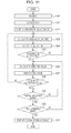
- FIG. 10 is a flow chart illustrating an example of setting processing of the debugger device.
- the debugger device 20 acquires one or more detection-target sequences input by operation of the key board 25 a or the mouse 25 b by the operator 20 a (Step S 10 ).
- the detection-target sequence may include the don't-care value in addition to the designated value.
- TCP transmission control protocol
- the debugger device 20 After acquiring the detection-target sequence, the debugger device 20 divides the detection-target sequence into the leading sequence Sa including no don't-care value and remaining sequences Sb 1 to Sbn ⁇ 1 that may include the don't-care value (Step S 11 ).
- the debugger device 20 calculates code values obtained by coding the sequence Sa and the designated value sequences Sba 1 to Sban ⁇ 1 in the sequences Sb 1 to Sbn ⁇ 1 according to CRC (Step S 12 ).
- the debugger device 20 calculates the code value from the first signal (for example, one byte of input data or output data) of the sequence Sa, and sequentially updates the code value according to subsequent signals.
- the code value is updated according to the last signal of the sequence Sa, the code value at this time becomes the code value of the sequence Sa.
- the sequences Sba 1 to Sban ⁇ 1 are similarly processed to calculate the code value.
- the debugger device 20 transmits information as illustrated in FIG. 4 , including the code value calculated in the processing in Step S 12 , to the semiconductor device 10 (Step S 13 ). Thereby, the debugger device 20 finishes setting processing.
- FIG. 11 is a flow chart illustrating an example of processing of the semiconductor device.
- the semiconductor device 10 receives the information such as the code value transmitted from the debugger device 20 by the reception circuit 13 (Step S 20 ). Then, a control circuit not illustrated in the semiconductor device 10 sets (stores) the received information in the registers 11 a 1 to 11 ap , 11 b 1 to 11 bp as illustrated in FIG. 4 (Step S 21 ).
- a control circuit not illustrated in the semiconductor device 10 causes the user circuit 12 to be debugged to start operation (Step S 22 ).
- the code value calculation circuit 11 c of the debug circuit 11 acquires the input data x or the output data y of the user circuit 12 in units of bytes, and calculates (updates) the code value according to CRC (Step S 23 ).
- first sequence detection circuit 11 e reads information recorded in the registers 11 a 1 to 11 ap to detect the sequence Sa (Step S 24 ).
- FIG. 12 is a view illustrating an example of detection of the sequence Sa.
- a sequence X is followed by the detection-target sequence S.
- FIG. 12 illustrates the example of the code values calculated by the code value calculation circuit 11 c .
- the code value finally calculated in the sequence X is CRC(X)
- the code value finally calculated in the sequence Sa is CRC(X&Sa).
- H(m) is a regular matrix that converts the value of CRC so as to achieve the same effect as &0 m .
- An example of CRC calculation using the regular matrix H is described in the non-patent document 1, for example.
- the shift register 11 d outputs the code value a(j ⁇ m) preceding the code value a(j) by m counts.
- the first sequence detection circuit 11 e determines whether or not the sequence Sa is detected by determining whether or not the expression (2) based on such CRC difference (change in the code value coded by CRC) (Step S 25 ).
- the count value is j
- the final signal in the sequence Sa is detected. Consequently, when the expression (2) holds, the first sequence detection circuit 11 e determines that the sequence Sa is detected, and transmits the code value a(j) to the expected value calculation circuit 11 f.
- Step S 23 When the sequence Sa is not detected, that is, when the expression (2) does not hold, the processing in Step S 23 and subsequent steps is repeated.
- the expected value calculation circuit 11 f calculates the expected value (Step S 26 ).
- FIG. 13 is a view illustrating an example of calculation of the expected value.
- the sequence Sb 1 occurs following the sequence Sa, if the count value is j+Len(Sba 1 ), CRC(X&Sa&Sba 1 ) that is the expected value of the code value b(j+Len(Sba 1 )) is expressed by a following expression.
- CRC(Sba 1 ) is the code value of the sequence Sba 1 , and is stored in any of the registers 11 b 1 to 11 bp.
- the expected value calculation circuit 11 f reads the code value of the sequence Sba 1 having the same identification information BPid as the sequence Sa from any of the registers 11 b 1 to 11 bp , and calculates the expected value by the expression (3).
- the code value calculation circuit 11 c updates the code value (Step S 27 ), and the match determination circuit 11 h 1 determines whether or not the code value output from the code value calculation circuit 2 b matches the expected value (Step S 28 ).
- the match determination circuit 11 h 1 determines that the code value output from the code value calculation circuit 2 b does not match the expected value, the processing in Step S 23 and subsequent steps is repeated.
- the match determination circuit 11 h 1 outputs a signal indicating the matching.
- the partial sequence end determination circuit 11 h 2 When receiving the signal, the partial sequence end determination circuit 11 h 2 acquires the length of the don't-care value sequence from the registers 11 b 1 to 11 bp . Then, based on the length, the partial sequence end determination circuit 11 h 2 determines whether or not any of the sequences Sb 1 to Sbn ⁇ 1 (partial sequence) ends (Step S 29 ). The processing in Step S 29 is repeated until any of the sequences Sb 1 to Sbn ⁇ 1 ends.
- FIG. 14 is a view illustrating sequence end determination processing. It is assumed that the partial sequence end determination circuit 11 h 2 receives a signal indicating that the code value matches the expected value when the count value is j+Len(Sba 1 ). At this time, the partial sequence end determination circuit 11 h 2 reads a length Len(X 1 ) of the don't-care value sequence X 1 , which has the same identification information BPid as the sequence Sba 1 , from any of the registers 11 b 1 to 11 bp . Here, Len(X 1 ) is expressed as the number of counts (or the number of bytes). The partial sequence end determination circuit 11 h 2 holds a value found by adding Len(X 1 ) to j+Len(Sba 1 ).
- the partial sequence end determination circuit 11 h 2 When the count value is updated to j+Len(Sba 1 )+Len(X 1 ), the partial sequence end determination circuit 11 h 2 outputs a signal indicating the end of the sequence Sba. When the partial sequence end determination circuit 11 h 2 outputs the signal indicating the end of any of the sequences Sb 1 to Sbn ⁇ 1, the final sequence determination circuit 11 h 3 determines whether or not the final sequence (sequence Sbn ⁇ 1) ends (Step S 30 ).
- Step S 26 determines that the final sequence does not end, the processing in Step S 26 and subsequent steps are performed again. For example, when the count value is j+Len(Sba 1 )+Len(X 1 ) as illustrated in FIG. 14 , only the sequence up to the sequence Sb 1 ends and thus, the processing of calculating the expected value in Step S 26 is performed. At this time, the expected value calculation circuit 11 f refers to a value of the pointer Next as illustrated in FIG. 4 to acquire information on the next sequence Sb 2 .
- the expected value at end of the designated value sequence Sba 2 in the sequence Sb 2 is calculated based on the code value a(j+Len(Sba 1 )+Len(X 1 )) and the code value CRC(Sba 2 ) of the sequence Sba 2 .
- the code value a(j+Len(Sba 1 )+Len(X 1 )) corresponds to CRC(X&Sa&Sb 1 ).
- the final sequence determination circuit 11 h 3 When determining the end of the final sequence, the final sequence determination circuit 11 h 3 outputs a signal indicating detection of the detection-target sequence S, and stops operation of the user circuit 12 to be debugged using the signal (Step S 31 ). In this manner, the processing of stopping the user circuit 12 at detection of the detection-target sequence is finished.
- the final sequence determination circuit 11 h 3 outputs “1” and stops supply of a clock signal to the user circuit 12 , thereby stopping operation of the user circuit 12 .
- the final sequence determination circuit 11 h 3 may block inputting data to the user circuit 12 or outputting data from the user circuit 12 to stop the user circuit 12 .
- the debugger device 20 performs debugging including check of the signal state of each unit of the user circuit 12 .
- debugging including check of the signal state of each unit of the user circuit 12 .
- FIG. 15 is a view illustrating an example of transition of input data.
- the input data x transitions in a sequence “YABABDCC”.
- t 1 to t 8 each denotes a count value (corresponding to time).
- a detection result of each of the divided sequences Sa, Sba 1 (a designated value sequence in the sequence Sb 1 , that is, “B”), and a detection result of Sb 2 are as follows.
- FIG. 16 is a view illustrating an example of the detection and end determination result of each sequence in the processing of detecting the detection-target sequence.
- FIG. 16 illustrates the detection results of the sequence Sa, Sba 1 , Sb 2 and the end determination results of the sequences Sb 1 , Sb 2 at each time. “1” indicates that the sequences Sa, Sba 1 , Sb 2 are detected, or the sequence Sb 1 ends. Since the sequence Sb 2 includes no don't-care value, the detection result and the end determination result have the same value.
- the match determination circuit 11 h 1 determines that the expected value at the end of the sequence Sba 1 matches the code value output from the code value calculation circuit 11 c.
- the detection result of the sequence Sa is “1”.
- the detection result of the sequence Sba 1 returns to “0”.
- the end determination result of the sequence Sb 1 is “1”. This is because the partial sequence end determination circuit 11 h 2 detects an elapse of two counts corresponding to the length of the sequence X 1 including the don't-care values “??”.
- the detection result of the sequence Sba 1 is “1”.
- the semiconductor device 10 , the debug circuit 11 , and the debugger device 20 may achieve the same effect as the semiconductor device 1 , the debug circuit 2 , and the debugger device 4 in First embodiment.
- the processing of stopping the user circuit 12 may be performed based on the code value of each of the sequence Sa and the sequences Sba 1 to Sban ⁇ 1 in a plurality of detection-target sequences, and lengths of the sequence X 1 to Xn ⁇ 1 and therefore, the user circuit 12 may be stopped under a plurality of stop conditions.
Abstract
A circuit includes don't-care a code-value calculation circuit to calculate third code-values by coding a signal sequence in accordance with a coding scheme; a first sequence-detection circuit to detect a first sequence based on comparison of a first code-value with a difference between the current third code-value and a fourth code-value that is the third code-value preceding the current third code-value by a length of the first sequence; an expected-value calculation circuit to calculate an expected value of the third code-value at the end of the third sequence based on a second code-value and a fifth code-value that is one of the third code-values; and a determination circuit to detect the end of the second sequence based on a length of a fourth sequence, notify an expected-value calculation circuit of the detection of the second sequence, and output a detection signal indicating detection of a detection-target sequence.
Description
This application is based upon and claims the benefit of priority of the prior Japanese Patent Application No. 2015-094556, filed on May 7, 2015, the entire contents of which are incorporated herein by reference.
The embodiments discussed herein relate to a debug circuit, a semiconductor device, and a debug method.
One of actual-hardware debugging systems for checking whether or not actual hardware normally operates is a logic analyzer in which a debug circuit is inserted at mounting of a debug-target circuit, and performs debugging.
In the logic analyzer, the debug circuit monitors a signal sequence (signal transition) of the debug-target circuit designated by the user. Then, when the signal sequence matches a predetermined stop condition, the debug circuit stops operation of the circuit, and outputs the signal sequence stored in a trace memory to a display or the like.
The related techniques are disclosed in Japanese Laid-open Patent Publication Nos. 2008-250442, 2004-086910, and 2009-289106, and M. Walma, “Pipelined Cyclic Redundancy Check (CRC) Calculation”, Proc. of 16th Int'l Conf. on Computer Communications and Networks, pp. 365-370, 2007.
In the case of software debugging, a program may be stopped in response to various conditions by using break points. In contrast, in the case of hardware debugging, it is difficult to stop the hardware under conditions or at timings desired by a user due to hardware constraints such as the capacity of the trace memory and the number of signal lines usable for debugging. In such a situation, improvement in working efficiency at debugging is a challenging issue.
According to an aspect of the invention, a debug circuit includes a memory configured to store, among code values calculated in accordance with a coding scheme that varies code values according to a signal sequence in a debug-target circuit, a first code value obtained by coding a leading first sequence of a plurality of sequences divided from a detection-target sequence detected from the signal sequence, a second code value obtained by coding a third sequence being a designated value sequence in each of two or more second sequences of the plurality of sequences, and a length of a fourth sequence being a don't-care value sequence in each of the second sequences; a code value calculation circuit configured to calculate third code values by coding the signal sequence in accordance with the coding scheme; a first sequence detection circuit configured to detect the first sequence based on comparison of the first code value with a difference between the current third code value and a fourth code value that is the third code value preceding the current third code value by a length of the first sequence; an expected value calculation circuit configured to calculate an expected value of the third code value at the end of the third sequence based on the second code value and a fifth code value that is one of the third code values at a time when the first sequence or the second sequence is detected; and a determination circuit configured to detect the end of the second sequence based on a length of the fourth sequence when the third code value matches the expected value, notify the expected value calculation circuit of the detection of the second sequence, and output a detection signal indicating detection of the detection-target sequence when the end of all the second sequences is detected.
The object and advantages of the invention will be realized and attained by means of the elements and combinations particularly pointed out in the claims.
It is to be understood that both the foregoing general description and the following detailed description are exemplary and explanatory and are not restrictive of the invention, as claimed.
Embodiments for carrying out the disclosure will be described below with reference to figures. FIG. 1A is a view illustrating an example of a semiconductor device, debug circuit, and a debugger device in First embodiment.
A semiconductor device 1 includes a debug circuit 2 and a debug-target circuit 3. The debug-target circuit 3 is, for example, hardware that transmits and receives data, and performs calculation. The debug circuit 2 detects a predetermined signal sequence (hereinafter referred to a detection-target sequence), which serves as a stop condition of the debug-target circuit 3, from any signal sequence in the debug-target circuit 3, and outputs a detection signal indicating that the detection-target sequence is detected. The detection signal is used to stop operation of the debug-target circuit 3, for example.
The detection-target sequence may include a designated value and a don't-care value that does not affect a detection result of the detection-target sequence. Thus, the don't-care value may be any value. For example, the don't-care value is set for a value that is unknown at debugging or the like. Information on a length of a sequence including such don't-care values (hereinafter, also referred to as a don't-care value sequence) is provided from, for example, a debugger device 4.
The debug circuit 2 in this embodiment may set the signal sequence including such don't-care value as a detection target. FIG. 1B illustrates an example of a detection-target sequence S. A plurality of elliptical elements each denote the designated value or the don't-care value. In the example in FIG. 1B , the detection-target sequence S is divided into three sequences Sa, Sb1, and Sb2, and the second sequence Sb1 includes a designated value sequence having a length L1, and a don't-care value sequence having a length L2. Among the divided sequences of the detection-target sequence S, the leading sequence Sa and the tailing sequence Sb2 do not include the don't-care value. The lengths L1, L2 of the sequences are expressed as the number of bytes, for example.
The detection-target sequence S may be divided into four or more sequences. The debug circuit 2 has a memory 2 a, a code value calculation circuit 2 b, a delay circuit 2 c, a first sequence detection circuit 2 d, an expected value calculation circuit 2 e, and a determination circuit 2 f. The memory 2 a may include a volatile storage medium and a nonvolatile storage medium. Examples of the volatile storage medium include a random access memory (RAM). The nonvolatile storage medium may include at least one of a hard disc drive (HDD), a solid state drive (SSD), an electrically erasable programmable read-only memory (EEPROM), and a flash memory. The debug circuit 2 further includes a counter 2 g that counts the number of data (e.g. the number of bytes) of input data x input to the debug-target circuit 3 and output data y output from the debug-target circuit 3.
The memory 2 a stores a code value Aa obtained by coding the sequence Sa, code values Ab1, Ab2 obtained by coding designated value sequences in the sequences Sb1, Sb2, and the length L2 of a don't-care value sequence. The memory 2 a may further store lengths of the designated value sequences Sa, Sb1, and Sb2, and identification information of the detection-target sequence S.
The code values Aa, Ab1, and Ab2 are calculated in accordance with a coding scheme that varies the code value according to the signal sequence in the debug-target circuit 3. The code values Aa, Ab1, and Ab2 are, for example, code values (linear codes) having linearity, and are calculated by the debugger device 4 in accordance with a coding scheme such as Cyclic Redundancy Check (CRC).
The code value calculation circuit 2 b calculates the code value according to the signal sequence of the debug-target circuit 3, in accordance with the same coding scheme as the coding scheme used when the debugger device 4 calculates the code values Aa, Ab1, and Ab2. For example, the code value calculation circuit 2 b acquires the signal of the debug-target circuit 3 (input data x or output data y) in units of bytes, and updates the code value. In this case, the detection-target sequence S is a sequence in units of bytes.
The delay circuit 2 c outputs a code value that is calculated by the code value calculation circuit 2 b at an earlier time by a period corresponding to a length of the sequence Sa in the detection-target sequence S. For example, the delay circuit 2 c is a shift register, and holds each of the code values calculated by the code value calculation circuit 2 b for the length of the sequence Sa, and outputs the code values one after another from the firstly input code value. That is, the delay circuit 2 c functions of delaying outputting of the input code values.
Here, the length of the sequence Sa is m counts (that is, m bytes). FIG. 1A illustrates the example in which the delay circuit 2 c outputs a code value a(j−m). The code value a(j−m) is a code value preceding from a code value a(j) by m counts.
The first sequence detection circuit 2 d compares a difference between the code value output from the code value calculation circuit 2 b and the code value output from the delay circuit 2 c with the code value Aa, and detects the leading sequence Sa in the plurality of sequences divided from the detection-target sequence S based on the comparison. That is, the first sequence detection circuit 2 d detects the sequence Sa based on comparison between the change in the code values of m counts and the code value Aa.
For example, when the difference between the code value output from the code value calculation circuit 2 b and the code value output from the delay circuit 2 c corresponds to the code value Aa, the first sequence detection circuit 2 d detects that the signal of the debug-target circuit 3 transitions in the sequence Sa.
When detecting the sequence Sa, the first sequence detection circuit 2 d supplies the code value output from the code value calculation circuit 2 b at detection to the expected value calculation circuit 2 e. In the example illustrated in FIG. 1A , the code value a(j) is supplied to the expected value calculation circuit 2 e.
The expected value calculation circuit 2 e calculates an expected value of the code value calculated by the code value calculation circuit 2 b at the end of the designated value sequence in the sequence Sb1 based on the code value output at detection of the sequence Sa among the code values calculated by the code value calculation circuit 2 b, and a code value Ab1. The expected value calculation circuit 2 e calculates an expected value of the code value calculated by the code value calculation circuit 2 b at the end of the designated value sequence in the sequence Sb2 based on the code value output at detection of the sequence Sb1 among the code values calculated by the code value calculation circuit 2 b, and a code value Ab2.
For example, when the code value output at detection of the sequence Sa is the code value a(j), the expected value calculation circuit 2 e calculated an expected value b(j+L1) according to an XOR of the code value a(j) and the code value Ab1. An example of an expression of calculating the expected value will be described later (refer to expression (3)).
When the code value output from the code value calculation circuit 2 b matches the expected value, the determination circuit 2 f detects the end of the sequences Sb1, Sb2 based on the length of the don't-care value sequence, and notifies the detection to the expected value calculation circuit 2 e.
In the example in FIG. 1B , the sequence Sb1 includes the don't-care values, and the length of the don't-care value sequence is L2. When the count value becomes a sum (j+L1+L2) of L2 and a count value (j+L1) at a time when the code value output from the code value calculation circuit 2 b matches the expected value b(j+L1), the determination circuit 2 f determines the end of the sequence Sb1. The sequence Sb2 does not include the don't-care value and thus, the length of the don't-care value sequence is 0. Accordingly, when the count value becomes a value at a time when the code value output from the code value calculation circuit 2 b matches the expected value, the determination circuit 2 f determines the end of the sequence Sb2.
When detecting the end of all the sequences Sb1, Sb2, the determination circuit 2 f outputs a signal indicating detection of the detection-target sequence. For example, as illustrated in FIG. 1A , the determination circuit 2 f includes a match determination circuit 2 f 1, a partial sequence end determination circuit 2 f 2, and a final sequence determination circuit 2 f 3.
The match determination circuit 2 f 1 determines whether or not the expected value calculated by the expected value calculation circuit 2 e matches the code value calculated by the code value calculation circuit 2 b. The partial sequence end determination circuit 2 f 2 acquires the length of the don't-care value sequence from the memory 2 a, and determines whether or not the sequences Sb1, Sb2 end based on the length. For example, when the count value in the counter 2 g increases from the count value at a time when the match determination circuit 2 f 1 detects matching between the code value and the expected value, by a count number corresponding to the length of the don't-care value sequence, the partial sequence end determination circuit 2 f 2 determines that the sequences Sb1, Sb2 end. In the above-mentioned example, when the count value is (j+L1+L2), the end of the sequence Sb1 is determined.
When determining the end of the sequences Sb1, Sb2, the partial sequence end determination circuit 2 f 2 notifies the expected value calculation circuit 2 e and the final sequence determination circuit 2 f 3 of the detection of the sequences Sb1, Sb2.
The final sequence determination circuit 2 f 3 detects the number of sequences divided from the detection-target sequence S, from information stored in the memory 2 a. The number of divided sequences itself may be stored in the memory 2 a, and in this case, the final sequence determination circuit 2 f 3 may acquire the number of sequences thus stored. Then, based on the number of sequences, the final sequence determination circuit 2 f 3 determines whether or not the end of all the sequences Sb1, Sb2 is notified by the partial sequence end determination circuit 2 f 2. When determining that the end of all the sequences Sb1, Sb2 is notified, the final sequence determination circuit 2 f 3 outputs a signal indicating detection of the detection-target sequence. This signal serves as a circuit stop signal that instructs stop of operation of the debug-target circuit 3.
The final sequence determination circuit 2 f 3 stops supply of a clock signal to the debug-target circuit 3 in response to the circuit stop signal, thereby stopping operation of the debug-target circuit 3. The final sequence determination circuit 2 f 3 may block inputting of data to the debug-target circuit 3 or outputting data from the debug-target circuit 3 to stop the debug-target circuit 3.
The debugger device 4 illustrated in FIG. 1A communicates with the semiconductor device 1 to perform debugging. The debugger device 4 is, for example, a computer, and executes following processing using software. The debugger device 4 first acquires the detection-target sequence S from a user (debug operator) (Step S1). Next, the debugger device 4 divides the detection-target sequence S into the sequences Sa, Sb1, and Sb2 as illustrated in FIG. 1B (Step S2). The debugger device 4 calculates the code values Aa, Ab1, and Ab2 obtained by coding the designated value sequences in the sequences Sa, Sb1, and Sb2, respectively (Step S3). Then, the debugger device 4 outputs (transmits) information on the sequences Sa, Sb1, and Sb2, which includes the calculated code values Aa, Ab1, and Ab2 and the length L2 of the don't-care value sequence, to the semiconductor device 1 (Step S4).
Hereafter, description is provided for an example of a debug method using a debug system including the semiconductor device 1 and the debugger device 4. The information of the sequences Sa, Sb1, and Sb2, which is calculated and transmitted by the debugger device 4 in the processing in Step S1 to S4 is stored in the memory 2 a in the debug circuit 2 of the semiconductor device 1.
The debug circuit 2 detects transition of the signal of the debug-target circuit 3, and in the example illustrate in FIG. 1A , the code value calculation circuit 2 b updates the code value based on the sequence of the input data x or the output data y.
For example, when the input data x or the output data y transitions from the state D(i) to D(i), D(j), and D(j+L1) as illustrated in FIG. 1C , the output of the code value calculation circuit 2 b is updated from the code value a(i) to a(j), and a(j+L1).
When the code value a(j) is output from the code value calculation circuit 2 b, a difference between the code value a(j) and code value a(j−m) output from the delay circuit 2 c corresponds to the code value Aa, the first sequence detection circuit 2 d supplies the code value a(j) to the expected value calculation circuit 2 e. The expected value calculation circuit 2 e calculates the expected value b(j+L1) based on the code value a(j) and the code value Ab1.
When the match determination circuit 2 f 1 detects matching between the code value output from the code value calculation circuit 2 b a(j+L1) and the expected value b(j+L1), the partial sequence end determination circuit 2 f 2 detects the end of the sequence Sb1 when the count value is (j+L1+L2).
Then, the expected value calculation circuit 2 e calculates the expected value at the end of the sequence Sb2 in the same manner based on the code value a(j+L1+L2) and the code value Ab2. When the match determination circuit 2 f 1 detects matching between the expected value and the code value output from the code value calculation circuit 2 b, since the length of the don't-care value sequence in the sequence Sb2 is 0, the partial sequence end determination circuit 2 f 2 detects the end of the sequence Sb2. When the end of the sequence Sb2 is detected, the final sequence determination circuit 2 f 3 outputs a signal indicating detection of the detection-target sequence S. This signal stops operation of the debug-target circuit 3.
After that, for example, the debugger device 4 performs debugging including check of the signal state of each unit of the debug-target circuit 3. As described above, the debug circuit 2 in this embodiment detects the sequence Sb1 including the don't-care values based on the code value Ab1 for the designated values and the length L2 of the don't-care value sequence, without considering the code value for the don't-care values calculated by the code value calculation circuit 2 b. Thereby, even the signal sequence including the don't-care values may be set as a detection target, increasing the degree of freedom in setting the detection-target sequence. For this reason, the working efficiency at debugging is improved.
With limitation in terms of hardware, the debug-target circuit 3 may be readily stopped under various conditions by adopting the above-mentioned code value, improving the working efficiency at debugging. Because the debug circuit 2 executes processing using a code value having a small amount of data, in place of directly handing input data x or output data y, the processing may be executed by a small-size circuit at higher speed.
Further, even when a complicated sequence is the detection-target sequence, since the sequence may be expressed as code values, the capacity of the memory 2 a may be decreased to reduce circuit areas of the debug circuit 2 and the semiconductor device 1.
At change of a detection-target sequence, the memory 2 a only has to store the code value obtained by coding the detection-target sequence. Hence, reinstallation of the circuit is not desirable, improving the working efficiency at debugging.
The debug system includes a semiconductor device 10 and a debugger device 20, and the semiconductor device 10 is connected to the debugger device 20 via a communication cable 20 b. The semiconductor device 10 may wirelessly communicate with the debugger device 20.
The semiconductor device 10 is, for example, a system on chip (SoC), and includes a debug circuit 11 and a user circuit 12 to be debugged. The debugger device 20 is, for example, a computer, and is operated by an operator 20 a and communicates with the semiconductor device 10 via the communication cable 20 b to perform debugging.
The debug circuit 11 includes registers 11 a 1 to 11 ap, registers 11 b 1 to 11 bp, a code value calculation circuit 11 c, a shift register 11 d, a first sequence detection circuit 11 e, an expected value calculation circuit 11 f, registers 11 g 1 to 11 gp, a determination circuit 11 h, and a counter 11 i.
The registers 11 a 1 to 11 ap and the registers 11 b 1 to 11 bp have a function of the memory 2 a in the debug circuit 2 in First embodiment. In place of the registers 11 a 1 to 11 ap and the registers 11 b 1 to 11 bp, a random access memory (RAM) may be used.
The registers 11 a 1 to 11 ap stores information on the code value obtained by coding the leading sequence having no don't-care value among the divided sequences in each of a plurality of (p) detection-target sequences. Hereinafter, as in First embodiment, a certain detection-target sequence, and a leading sequence among sequences divided from the detection-target sequence are denoted by the detection-target sequence S and the sequence Sa, respectively.
The registers 11 b 1 to 11 bp stores code values obtained by coding remaining sequences among the divided plurality of sequences, and information such as the length of the don't-care value sequence. Hereinafter, the number of the remaining sequences is denoted by n−1, and the remaining sequences are expressed as sequences Sb1 to Sbn− 1. Then, n denotes the number of divided sequences, and n is 1 or more (where n=1 indicates no division). Hereinafter, the code value is coded by CRC, but the code value is not limited to this, and may be a code value having linearity.
The register 11 b 1 stores information on the sequences Sb1 to Sbn−1 of the detection-target sequence. FIG. 4 illustrates an example of storage of information on the ith sequence Sbi among the sequences Sb1 to Sbn− 1. The register 11 b 1 stores identification information BPid of the detection-target sequence S including the sequence Sbi, a code value CRC(Sbai) of a designated value sequence Sbai included in the sequence Sbim and a length Len(Sbai) of the sequence Sbai. The register 11 b 1 further stores a length Len(Xi) of the don't-care value sequence Xi included in the sequence Sbi, and a pointer Next designating a storage location of information on i+1th sequence Sbi+ 1.
The identification information BPid is used to indicate that the sequence Sa and the sequence Sbai are included in the same detection-target sequence. In a below-mentioned example, the lengths Len(Sa), Len(Sbai), and Len(Xi) are expressed as the number of bytes. When the counter 11 i counts up at a cycle of one clock, and the code value calculation circuit 11 c calculates the code value at the clock cycle, the above length information is expressed in units of clock cycle.
The pointer Next included information on a n−1th sequence Sbn−1 has a value indicating the final sequence (for example, “Null”). The detection-target sequence designates the transition mode of a signal on the user circuit 12 to stop the user circuit 12. The signal on the user circuit 12 is input data or output data of the user circuit 12, or an internal signal. Although the detection-target sequence will be hereinafter described as transition of one signal (for example, input data or output data), the sequence may be transition of a combination of a plurality of signals.
Based on the signal sequence on the user circuit 12, the code value calculation circuit 11 c calculates the code value changed by the sequence according to the same coding scheme (that is, CRC) as the coding scheme used to calculate the code values in the debugger device 20.
The shift register 11 d has the same function as the delay circuit 2 c in the debug circuit 2 in First embodiment. The shift register 11 d holds the code values calculated by the code value calculation circuit 11 c within a time corresponding to the length of the sequence Sa, and outputs them one after another from the firstly input code value. As in First embodiment, the length of the sequence Sa is set to m counts. For example, m is determined based on the capacity of the shift register 11 d.
The first sequence detection circuit 11 e detects the sequence Sa based on comparison of the difference between the code value output from the code value calculation circuit 11 c and the code value output from the shift register 11 d, with the code value stored in the registers 11 a 1 to 11 ap.
When detecting the sequence Sa, the first sequence detection circuit 11 e supplies the code value at detection to the expected value calculation circuit 11 f. Further, when detecting the sequence Sa, the first sequence detection circuit 11 e sends a signal indicating the detection signal (for example, “1”) to a final sequence determination circuit 11 h 3.
The expected value calculation circuit 11 f calculates the expected value of the code value calculated by the code value calculation circuit 11 c at the end of the sequences Sba1 to Sban−1, based on the code value output at detection of the sequence Sa and the code values stored in the registers 11 b 1 to 11 bp. The sequences Sba1 to Sban−1 are designated value sequences included in the sequences Sb1 to Sbn− 1.
The registers 11 g 1 to 11 gp stores expected values corresponding to p detection-target sequences, which are calculated by the expected value calculation circuit 11 f. FIG. 5 is a view illustrating an example of storage of the expected value in the register.
The register 11 g 1 stores the expected value of the code value at the end of each of the designated value sequences Sba1 to Sban−1 in the sequences Sb1 to Sbn−1, the expected value calculated by the code value calculation circuit 11 c. In the example illustrated in FIG. 5 , an expected value CRC(X&Sa&Sba1) at the end of the sequence Sba1, the identification information BPid of the detection-target sequence S, and the pointer Next indicating the storage location of information on the next sequence Sba2 are stored. Here, “&” indicates connection of sequences. X is an unknown sequence, and the expected value CRC(X&Sa&Sba1) denotes the expected value of the code value acquired when the unknown sequence X is followed by the sequence Sa and the sequence Sba1.
The determination circuit 11 h illustrated in FIG. 3 includes a match determination circuit 11 h 1, a partial sequence end determination circuit 11 h 2, and a final sequence determination circuit 11 h 3. The match determination circuit 11 h 1 determines whether or not the expected values stored in the registers 11 g 1 to 11 gp match the code value calculated by the code value calculation circuit 11 c.
The partial sequence end determination circuit 11 h 2 acquires the length of the don't-care value sequence from the registers 11 b 1 to 11 bp, and determines whether or not the sequences Sb1 to Sbn−1 end based on the length. Every time the partial sequence end determination circuit 11 h 2 determines the end of any of the sequences Sb1 to Sbn−1, the partial sequence end determination circuit 11 h 2 notifies the expected value calculation circuit 11 f and the final sequence determination circuit 11 h 3 of detection of the sequence Sb1 to Sbn− 1.
The final sequence determination circuit 11 h 3 detects the number of sequences divided from the detection-target sequence S, from information stored in the registers 11 b 1 to 11 bp. The number of sequences itself may be stored in the registers 11 b 1 to 11 bp or the registers 11 a 1 to hap, and in this case, the final sequence determination circuit 11 h 3 acquires the number of sequences.
Then, based on the number of sequences, the final sequence determination circuit 11 h 3 determines whether or not the partial sequence end determination circuit 11 h 2 notifies the end of all the sequences Sb1 to Sbn− 1. When determining that the end of all the sequences Sb1 to Sbn−1 is notified, the final sequence determination circuit 11 h 3 outputs a signal indicating detection of the detection-target sequence S. This signal serves as a circuit stop signal that instructs stop of operation of the for example, debug-target circuit 3. When receiving notification of the end of the sequence Sbn−1, the final sequence determination circuit 11 h 3 may refer to the pointer Next (“NULL”) included in the information on the sequence Sbn−1 to determine the end of all the sequences Sb1 to Sbn− 1.
The match determination circuit 11 h 1, the partial sequence end determination circuit 11 h 2, and the final sequence determination circuit 11 h 3 in the determination circuit 11 h are embodied as follows. FIG. 6 is a view illustrating an example of the match determination circuit.
The match determination circuit 11 h 1 includes n−1 comparators 14 a 1 to 14 an−1. The comparators 14 a 1 to 14 an−1 determines whether or not n−1 expected values of the detection-target sequence S, which are stored in the register 11 g 1, with the code value calculated by the code value calculation circuit 11 c. For example, the comparator 14 a 1 compares the expected value CRC(X&Sa&Sba1) at the end of the sequence Sba1 with the code value calculated by the code value calculation circuit 11 c, and outputs “1” when they match each other.
The n−1 expected values of other detection-target sequences stored in the registers 11 g 1 to 11 gp except for the register 11 g 1 may be also used in the above circuit for matching determination. In this case, a selection circuit for selecting an output of any of the registers 11 g 1 to 11 gp is provided.
The adder circuits 15 a 1 to 15 an−1 add the lengths of the don't-care value sequences X1 to Xn−1 included in the sequences Sb1 to Sbn−1, which are stored in the register 11 b 1, to the count value of the counter 11 i.
The buffers 16 a 1 to 16 an−1 receive the respective addition results of the adder circuits 15 a 1 to 15 an−1, and each output the addition result when receiving, from the match determination circuit 11 h 1, a signal indicating matching between the expected value and the code value for the corresponding one of the sequences Sb1 to Sbn− 1. The addition result at this time corresponds to the count value at the end of the corresponding sequence Sb1 to Sbn− 1.
The registers 17 a 1 to 17 an−1 store the addition results. The comparators 18 a 1 to 18 an−1 determines whether or not the respective added values stored in the registers 17 a 1 to 17 an−1 match the count value of the counter 11 i. For example, the comparator 18 a 1 compares the added value stored in the register 17 a 1, which corresponds to the count value at the end of the sequence Sb1, with the current count value of the counter 11 i, and outputs “1” when they match each other.
Lengths of the don't-care value sequence in other detection-target sequences, which are stored in the registers 11 b 1 to 11 bp except for the register 11 b 1, may be used in the above circuit for determination. In this case, selection circuit for selecting an output of any of registers 11 b 1 to 11 bp is provided.
For example, in the case of n=1, when receiving the signal indicating detection of the sequence Sa from the first sequence detection circuit 11 e, the multiplexer 19 outputs a signal indicating the end of the final sequence, that is the signal indicating detection of the detection-target sequence.
For example, in the case of n=3, when receiving a signal indicating the end of the sequence Sb2 from the partial sequence end determination circuit 11 h 2, the multiplexer 19 outputs a signal indicating the end of the final sequence, that is, a signal indicating detection of the detection-target sequence.
Examples of processing of the first sequence detection circuit 11 e, the expected value calculation circuit 11 f, and the determination circuit 11 h will be described later.
The debugger device 20 is a computer, and is controlled by a processor 21 as a whole. A RAM 22 and a plurality of peripheral devices are connected to the processor 21 via a bus 29. The processor 21 may be a multiprocessor. Examples of the processor 21 includes a central processing unit (CPU), a micro processing unit (MPU), a digital signal processor (DSP), an application specific integrated circuit (ASIC), and a programmable logic device (PLD). The processor 21 may be any combination of two or more of CPUs, MPUs, DSPs, ASICs, and PLDs.
The RAM 22 is used as a main memory of the debugger device 20. The RAM 22 temporarily stores at least a part of an OS (Operating System) program and an application program that are executed by the processor 21. The RAM 22 stores various data desirable for processing of the processor 21.
The peripheral devices connected to the bus 29 are a hard disk drive (HDD) 23, a graphic processor 24, an input interface 25, an optical drive 26, a device connecting interface 27, and a network interface 28.
The HDD 23 magnetically writes and reads data into and from an internal disc. The HDD 23 is used as an auxiliary memory of the debugger device 20. The HDD 23 stores an OS program, an application program, and various data. A semiconductor memory such as a flash memory may be used as an auxiliary memory.
A graphic processor 24 is connected to a monitor 24 a. The graphic processor 24 displays an image such as a debug result on a screen of the monitor 24 a according to an instruction of the processor 21. Examples of the monitor 24 a include a display using cathode ray tube (CRT) and a liquid crystal display.
The input interface 25 is connected to a key board 25 a and a mouse 25 b. The input interface 25 transmits a signal from the key board 25 a or the mouse 25 b to the processor 21. The mouse 25 b is an example of a pointing device, and another pointing device may be used. Examples of another pointing device include a touch panel, a tablet, a touch pad, and a track ball.
The optical drive 26 reads data recorded in an optical disc 26 a using laser light or the like. The optical disc 26 a is a portable recording medium in which data may be read by light reflection. Examples of the optical disc 26 a include a digital versatile disc (DVD), a DVD-RAM, a compact disc read only memory (CD-ROM), and a CD-R (Recordable)/RW (ReWritable).
The device connecting interface 27 is a communication interface for connecting the peripheral devices to the debugger device 20. For example, a memory 27 a and a memory reader-writer 27 b may be connected to the device connecting interface 27. The memory 27 a is a recording medium having a function of communicating with the device connecting interface 27. The memory reader-writer 27 b writes data to a memory card 27 c, and reads data from the memory card 27 c. The memory card 27 c is a card-type recording medium.
The device connecting interface 27 is connected to the semiconductor device 10 via the communication cable 20 b. The network interface 28 is connected to a network 28 a. The network interface 28 transmits and receives data to and from another computer or communication equipment via the network 28 a.
The hardware thus configured may execute processing of the debugger device 20 in Second embodiment. The debugger device 4 in First embodiment may be embodied by the same hardware as the debugger device 20 illustrated in FIG. 9 .
The debugger device 20 executes the program recorded in a computer-readable recording medium, thereby performing the processing in Second embodiment. The program that describes contents of the processing executed by the debugger device 20 may be recorded in various recording media. For example, the HDD 23 may store the program executed by the debugger device 20. The processor 21 loads at least a part of the program in the HDD 23 into the RAM 22 to execute the program. The program executed by the debugger device 20 may be also recorded in portable recording media such as the optical disc 26 a, the memory 27 a, and the memory card 27 c. The program stored in the portable recording media is installed to the HDD 23 under control of the processor 21 to become available. The processor 21 may read the program directly from the portable recording media, and executes the program.
An example of a debug method using the semiconductor device 10 and the debugger device 20 will be described below.
The detection-target sequence may include the don't-care value in addition to the designated value. For example, when the user circuit 12 processes a transmission control protocol (TCP) packet, a sequence number has a random initial value and thus, is set to the don't-care value.
After acquiring the detection-target sequence, the debugger device 20 divides the detection-target sequence into the leading sequence Sa including no don't-care value and remaining sequences Sb1 to Sbn−1 that may include the don't-care value (Step S11).
Then, the debugger device 20 calculates code values obtained by coding the sequence Sa and the designated value sequences Sba1 to Sban−1 in the sequences Sb1 to Sbn−1 according to CRC (Step S12). In the processing in Step S12, the debugger device 20 calculates the code value from the first signal (for example, one byte of input data or output data) of the sequence Sa, and sequentially updates the code value according to subsequent signals. When the code value is updated according to the last signal of the sequence Sa, the code value at this time becomes the code value of the sequence Sa. The sequences Sba1 to Sban−1 are similarly processed to calculate the code value.
The debugger device 20 transmits information as illustrated in FIG. 4 , including the code value calculated in the processing in Step S12, to the semiconductor device 10 (Step S13). Thereby, the debugger device 20 finishes setting processing.
After that, a control circuit not illustrated in the semiconductor device 10 causes the user circuit 12 to be debugged to start operation (Step S22). After start of operation of the user circuit 12, the code value calculation circuit 11 c of the debug circuit 11 acquires the input data x or the output data y of the user circuit 12 in units of bytes, and calculates (updates) the code value according to CRC (Step S23).
Then, first sequence detection circuit 11 e reads information recorded in the registers 11 a 1 to 11 ap to detect the sequence Sa (Step S24). FIG. 12 is a view illustrating an example of detection of the sequence Sa.
The linearity of CRC satisfies a following expression. CRC(X&Sa)=CRC((X&0m)+(0k&Sa))=CRC(X&0m)+CRC(0k&Sa)=CRC(X&0m)+CRC(Sa)=H(m)×CRC(X)+CRC(Sa) . . . (1)
In the expression (1), “+” denotes XOR (this applies to following expressions on CRC). “0m” denotes the sequence in which the signal of the user circuit 12 continues to 0 for m counts. Given that the length of the sequence X is k counts (k bytes), “0k” means the sequence in which the signal of the user circuit 12 continues to 0 for k counts.
CRC(X&0m)+CRC(0k&Sa)=CRC(X&0m)+CRC(Sa) in the expression (1) is due to that 0 continuing from the initial state does not affect the value of the CRC irrespective of the number of 0.
In the expression (1), H(m) is a regular matrix that converts the value of CRC so as to achieve the same effect as &0m. An example of CRC calculation using the regular matrix H is described in the non-patent document 1, for example.
It is given that the count value is j, and the code value calculated by the code value calculation circuit 11 c is a(j). When the count value is j, the shift register 11 d outputs the code value a(j−m) preceding the code value a(j) by m counts.
When receiving the code values a(j), a(j−m), the first sequence detection circuit 11 e evaluates whether or not a following conditional expression based on a difference between code values a(j) and a(j−m) holds. a(j)−H(m)×a(j−m)=CRC(Sa) . . . (2) Even if the sequence X starting from the count value of 0 is unknown, the conditional expression (2) holds when the sequence from the count value j−m+1 to j matches the sequence Sa.
The first sequence detection circuit 11 e determines whether or not the sequence Sa is detected by determining whether or not the expression (2) based on such CRC difference (change in the code value coded by CRC) (Step S25).
When the expression (2) holds, as illustrated in FIG. 12 , the code value a(j−m) becomes a(j−m)=CRC(X), the code value a(j) becomes a(j)=CRC(X&Sa), and when the count value is j, the final signal in the sequence Sa is detected. Consequently, when the expression (2) holds, the first sequence detection circuit 11 e determines that the sequence Sa is detected, and transmits the code value a(j) to the expected value calculation circuit 11 f.
When the sequence Sa is not detected, that is, when the expression (2) does not hold, the processing in Step S23 and subsequent steps is repeated. When receiving the code value a(j), the expected value calculation circuit 11 f calculates the expected value (Step S26).
CRC(X&Sa&Sba1)=CRC(X&Sa&0Len(Sba1))+CRC(Sba1)=H (Len(Sba1))×CRC(X&Sa)+CRC(Sba1) (3) CRC(Sba1) is the code value of the sequence Sba1, and is stored in any of the registers 11 b 1 to 11 bp.
Accordingly, the expected value calculation circuit 11 f reads the code value of the sequence Sba1 having the same identification information BPid as the sequence Sa from any of the registers 11 b 1 to 11 bp, and calculates the expected value by the expression (3).
Then, the code value calculation circuit 11 c updates the code value (Step S27), and the match determination circuit 11 h 1 determines whether or not the code value output from the code value calculation circuit 2 b matches the expected value (Step S28). When the match determination circuit 11 h 1 determines that the code value output from the code value calculation circuit 2 b does not match the expected value, the processing in Step S23 and subsequent steps is repeated. When the code value matches the expected value, the match determination circuit 11 h 1 outputs a signal indicating the matching.
When receiving the signal, the partial sequence end determination circuit 11 h 2 acquires the length of the don't-care value sequence from the registers 11 b 1 to 11 bp. Then, based on the length, the partial sequence end determination circuit 11 h 2 determines whether or not any of the sequences Sb1 to Sbn−1 (partial sequence) ends (Step S29). The processing in Step S29 is repeated until any of the sequences Sb1 to Sbn−1 ends.
When the count value is updated to j+Len(Sba1)+Len(X1), the partial sequence end determination circuit 11 h 2 outputs a signal indicating the end of the sequence Sba. When the partial sequence end determination circuit 11 h 2 outputs the signal indicating the end of any of the sequences Sb1 to Sbn−1, the final sequence determination circuit 11 h 3 determines whether or not the final sequence (sequence Sbn−1) ends (Step S30).
When the final sequence determination circuit 11 h 3 determines that the final sequence does not end, the processing in Step S26 and subsequent steps are performed again. For example, when the count value is j+Len(Sba1)+Len(X1) as illustrated in FIG. 14 , only the sequence up to the sequence Sb1 ends and thus, the processing of calculating the expected value in Step S26 is performed. At this time, the expected value calculation circuit 11 f refers to a value of the pointer Next as illustrated in FIG. 4 to acquire information on the next sequence Sb2. The expected value at end of the designated value sequence Sba2 in the sequence Sb2 is calculated based on the code value a(j+Len(Sba1)+Len(X1)) and the code value CRC(Sba2) of the sequence Sba2. The code value a(j+Len(Sba1)+Len(X1)) corresponds to CRC(X&Sa&Sb1).
When determining the end of the final sequence, the final sequence determination circuit 11 h 3 outputs a signal indicating detection of the detection-target sequence S, and stops operation of the user circuit 12 to be debugged using the signal (Step S31). In this manner, the processing of stopping the user circuit 12 at detection of the detection-target sequence is finished.
The final sequence determination circuit 11 h 3 outputs “1” and stops supply of a clock signal to the user circuit 12, thereby stopping operation of the user circuit 12. The final sequence determination circuit 11 h 3 may block inputting data to the user circuit 12 or outputting data from the user circuit 12 to stop the user circuit 12.
After that, for example, the debugger device 20 performs debugging including check of the signal state of each unit of the user circuit 12. An example in which a 5 bytes of detection-target sequence “AB??C” is detected by using the above debug method will be described below. “?” denotes the don't-care value, and other “A”, “B”, and “C” denote the designated value. It is given that the detection-target sequence is divided into three sequences Sa, Sb1, and Sb2: “A”, “B??”, and “C”. It is assumed that the input data x of the user circuit 12 transitions as follows.
When the above detection-target sequence is detected from such sequence of input data x, a detection result of each of the divided sequences Sa, Sba1 (a designated value sequence in the sequence Sb1, that is, “B”), and a detection result of Sb2 are as follows.
At Time t1, since the input data x is “Y”, the sequence Sa is not detected, and the detection results of the sequences Sa, Sba1, and Sb2 and the end determination result of the sequence Sb1 are all “0”.
At Time t2, since the input data x is “A”, the first sequence detection circuit 11 e detects the sequence Sa, and the detection result is “1”. At Time t3, since the input data x is “B”, the detection result of the sequence Sa is “0”, but the detection result of the sequence Sba1 is “1”. This is due to that the match determination circuit 11 h 1 determines that the expected value at the end of the sequence Sba1 matches the code value output from the code value calculation circuit 11 c.
At Time t4, since the input data x is “A” again, the detection result of the sequence Sa is “1”. The detection result of the sequence Sba1 returns to “0”. At Time t5 later by two counts than the time of detection of the sequence Sba1, the end determination result of the sequence Sb1 is “1”. This is because the partial sequence end determination circuit 11 h 2 detects an elapse of two counts corresponding to the length of the sequence X1 including the don't-care values “??”. At Time t5, since the input data x is “B”, the detection result of the sequence Sba1 is “1”.
At Time t6, since the input data x is “D”, both detection results of the sequences Sa, Sba are “0”. The end determination result of the sequence Sb1 is also “0”. At Time t7 later by two counts than the time of detection of the sequence Sba1 at Time t5 by two counts, the end determination result of the sequence Sb1 becomes “1” again.
Then, at Time t8, the input data x is “C”, and the detection result and the end determination result of the sequence Sb2 becomes “1”. That is, in the above example, at Time t8, the detection-target sequence is detected.
The semiconductor device 10, the debug circuit 11, and the debugger device 20 may achieve the same effect as the semiconductor device 1, the debug circuit 2, and the debugger device 4 in First embodiment. The processing of stopping the user circuit 12 may be performed based on the code value of each of the sequence Sa and the sequences Sba1 to Sban−1 in a plurality of detection-target sequences, and lengths of the sequence X1 to Xn−1 and therefore, the user circuit 12 may be stopped under a plurality of stop conditions.
Although the debug circuit, the semiconductor device, and the debug method according to an aspect of the disclosure has been described based on the embodiments, they are merely examples, and are not limited to the embodiments. All examples and conditional language recited herein are intended for pedagogical purposes to aid the reader in understanding the invention and the concepts contributed by the inventor to furthering the art, and are to be construed as being without limitation to such specifically recited examples and conditions, nor does the organization of such examples in the specification relate to a showing of the superiority and inferiority of the invention. Although the embodiments of the present invention have been described in detail, it should be understood that the various changes, substitutions, and alterations could be made hereto without departing from the spirit and scope of the invention.
Claims (6)
1. A debug circuit, comprising:
a memory configured to store, among code values calculated in accordance with a coding scheme that varies code values according to a signal sequence in a debug-target circuit, a first code value obtained by coding a leading first sequence of a plurality of sequences divided from a detection-target sequence detected from the signal sequence, a second code value obtained by coding a third sequence being a designated value sequence in each of two or more second sequences of the plurality of sequences, and a length of a fourth sequence being a don't-care value sequence in each of the second sequences;
a code value calculation circuit configured to calculate third code values by coding the signal sequence in accordance with the coding scheme;
a first sequence detection circuit configured to detect the first sequence based on comparison of the first code value with a difference between the current third code value and a fourth code value that is the third code value preceding the current third code value by a length of the first sequence;
an expected value calculation circuit configured to calculate an expected value of the third code value at the end of the third sequence based on the second code value and a fifth code value that is one of the third code values at a time when the first sequence or the second sequence is detected; and
a determination circuit configured to detect the end of the second sequence based on a length of the fourth sequence when the third code value matches the expected value, notify the expected value calculation circuit of the detection of the second sequence, and output a detection signal indicating detection of the detection-target sequence when the end of all the second sequences is detected.
2. The debug circuit according to claim 1 , wherein
the coding scheme is a scheme that calculates code values having linearity.
3. The debug circuit according to claim 1 , wherein
the determination circuit comprises:
a first determination circuit configured to compare the third code value with the expected value and determine whether or not they match each other;
a second determination circuit configured to detect the end of the second sequence when the third code value is updated the number of times corresponding to the length of the fourth sequence, after the first determination circuit determines that the third code value and the expected value match each other; and
a third determination circuit configured to determine whether or not all the second sequences end based on the number of the second sequences, every time the second determination circuit detects the end of the second sequence.
4. The debug circuit according to claim 1 , wherein
the detection-target sequence is configured to represent a stop condition of the circuit, and
the determination circuit stops operation of the circuit according to the detection signal.
5. A semiconductor device comprising:
a debug-target circuit; and
a debug circuit, wherein
the debug circuit comprises:
a memory configured to store, among code values calculated in accordance with a coding scheme that varies code values according to a signal sequence in the debug-target circuit, a first code value obtained by coding a leading first sequence of a plurality of sequences divided from a detection-target sequence detected from the signal sequence, a second code value obtained by coding a third sequence being a designated value sequence in each of two or more second sequences of the plurality of sequences, and a length of a fourth sequence being a don't-care value sequence in each of the second sequences;
a code value calculation circuit configured to calculate third code values by coding the signal sequence in accordance with the coding scheme;
a first sequence detection circuit configured to detect the first sequence based on comparison of the first code value with a difference between the current third code value and a fourth code value that is the third code value preceding the current third code value by a length of the first sequence;
an expected value calculation circuit configured to calculate an expected value of the third code value at the end of the third sequence based on the second code value and a fifth code value that is one of the third code values at a time when the first sequence or the second sequence is detected; and
a determination circuit configured to detect the end of the second sequence based on a length of the fourth sequence when the third code value matches the expected value, notify the expected value calculation circuit of the detection of the second sequence, and output a detection signal indicating detection of the detection-target sequence when the end of all the second sequences is detected.
6. A debug method using a debugger device including a computer, and a semiconductor device including a circuit as a debug target, the method comprising:
causing the debugger device to:
divide a detection-target sequence detected from a signal sequence in the circuit into a plurality of sequences,
calculate a first code value by coding a leading first sequence in the plurality of sequences in accordance with a coding scheme that varies code values according to the signal sequence, and a second code value by coding a third sequence being a designated value sequence in each of two or more second sequences of the plurality of sequences, and
transmit the first code value, the second code value, and a length of a fourth sequence being a don't-care value sequence in each of the second sequences; and
causing the semiconductor device to:
receive the first code value, the second code value, and the length of the fourth sequence,
calculate third code values by coding the signal sequence in accordance with the coding scheme,
detect the first sequence based on comparison of the first code value with a difference between the current third code value and a fourth code value that is the third code value preceding the current third code value by a length of the first sequence,
calculate an expected value of the third code value at the end of the third sequence based on the second code value and a fifth code value that is one of the third code values at a time when the first sequence or the second sequence is detected, and
detect the end of the second sequence based on a length of the fourth sequence when the third code value matches the expected value, and output a detection signal indicating detection of the detection-target sequence when the end of all the second sequences is detected.
Applications Claiming Priority (2)
| Application Number | Priority Date | Filing Date | Title |
|---|---|---|---|
| JP2015094556A JP6458626B2 (en) | 2015-05-07 | 2015-05-07 | Debug circuit, semiconductor device, and debugging method |
| JP2015-094556 | 2015-05-07 |
Publications (2)
| Publication Number | Publication Date |
|---|---|
| US20160327610A1 US20160327610A1 (en) | 2016-11-10 |
| US9720037B2 true US9720037B2 (en) | 2017-08-01 |
Family
ID=57222491
Family Applications (1)
| Application Number | Title | Priority Date | Filing Date |
|---|---|---|---|
| US15/085,298 Active US9720037B2 (en) | 2015-05-07 | 2016-03-30 | Debug circuit, semiconductor device, and debug method |
Country Status (2)
| Country | Link |
|---|---|
| US (1) | US9720037B2 (en) |
| JP (1) | JP6458626B2 (en) |
Cited By (1)
| Publication number | Priority date | Publication date | Assignee | Title |
|---|---|---|---|---|
| US20160282413A1 (en) * | 2015-03-27 | 2016-09-29 | Fujitsu Limited | Debug circuit, semiconductor device, and debug method |
Families Citing this family (2)
| Publication number | Priority date | Publication date | Assignee | Title |
|---|---|---|---|---|
| CN112703409A (en) * | 2019-01-22 | 2021-04-23 | 爱德万测试公司 | Automatic test equipment for testing one or more devices under test, method for automatically testing one or more devices under test, and computer program using buffer memory |
| US10949586B1 (en) * | 2020-07-01 | 2021-03-16 | Xilinx, Inc. | Post-synthesis insertion of debug cores |
Citations (4)
| Publication number | Priority date | Publication date | Assignee | Title |
|---|---|---|---|---|
| US20040040013A1 (en) | 2002-08-26 | 2004-02-26 | Mohit Kalra | Time-based breakpoints in debuggers |
| US20070226702A1 (en) * | 2006-03-22 | 2007-09-27 | Rolf Segger | Method for operating a microcontroller in a test environment |
| JP2008250442A (en) | 2007-03-29 | 2008-10-16 | Fujitsu Microelectronics Ltd | Trigger generation circuit |
| US20090300410A1 (en) | 2008-05-30 | 2009-12-03 | Fujitsu Limited | Semiconductor integrated circuit, control method, and information processing apparatus |
Family Cites Families (4)
| Publication number | Priority date | Publication date | Assignee | Title |
|---|---|---|---|---|
| JPH08314754A (en) * | 1995-05-22 | 1996-11-29 | Fujitsu Ltd | Trigger control circuit |
| JP2002202900A (en) * | 2000-12-28 | 2002-07-19 | Seiko Epson Corp | Debug device |
| JP4062546B2 (en) * | 2005-09-30 | 2008-03-19 | オムロン株式会社 | Debug device |
| JP2012003671A (en) * | 2010-06-21 | 2012-01-05 | Renesas Electronics Corp | Debugging device, debugging method, and debugger program |
-
2015
- 2015-05-07 JP JP2015094556A patent/JP6458626B2/en active Active
-
2016
- 2016-03-30 US US15/085,298 patent/US9720037B2/en active Active
Patent Citations (6)
| Publication number | Priority date | Publication date | Assignee | Title |
|---|---|---|---|---|
| US20040040013A1 (en) | 2002-08-26 | 2004-02-26 | Mohit Kalra | Time-based breakpoints in debuggers |
| JP2004086910A (en) | 2002-08-26 | 2004-03-18 | Internatl Business Mach Corp <Ibm> | Method, system, and software product for debugging computer program |
| US20070226702A1 (en) * | 2006-03-22 | 2007-09-27 | Rolf Segger | Method for operating a microcontroller in a test environment |
| JP2008250442A (en) | 2007-03-29 | 2008-10-16 | Fujitsu Microelectronics Ltd | Trigger generation circuit |
| US20090300410A1 (en) | 2008-05-30 | 2009-12-03 | Fujitsu Limited | Semiconductor integrated circuit, control method, and information processing apparatus |
| JP2009289106A (en) | 2008-05-30 | 2009-12-10 | Fujitsu Ltd | Semiconductor integrated circuit, its controlling method, and information-processing device |
Non-Patent Citations (1)
| Title |
|---|
| Walma, Mathys, "Pipelined Cyclic Redundancy Check (CRC) Calculation", Proc. of 16th Int'l Conf. on Computer Communications and Networks, 2007, pp. 365-370. |
Cited By (2)
| Publication number | Priority date | Publication date | Assignee | Title |
|---|---|---|---|---|
| US20160282413A1 (en) * | 2015-03-27 | 2016-09-29 | Fujitsu Limited | Debug circuit, semiconductor device, and debug method |
| US10024911B2 (en) * | 2015-03-27 | 2018-07-17 | Fujitsu Limited | Debug circuit, semiconductor device, and debug method |
Also Published As
| Publication number | Publication date |
|---|---|
| JP2016212574A (en) | 2016-12-15 |
| JP6458626B2 (en) | 2019-01-30 |
| US20160327610A1 (en) | 2016-11-10 |
Similar Documents
| Publication | Publication Date | Title |
|---|---|---|
| US11640247B2 (en) | Providing service address space for diagnostics collection | |
| US9720037B2 (en) | Debug circuit, semiconductor device, and debug method | |
| US9612837B2 (en) | Trace method and information processing apparatus | |
| US10024911B2 (en) | Debug circuit, semiconductor device, and debug method | |
| US20190385081A1 (en) | Anomaly detection model selection and validity for time series data | |
| US9753084B2 (en) | Debug circuit, semiconductor device, and debug method | |
| CN110580220B (en) | Method for measuring code segment execution time and terminal equipment | |
| US20160328290A1 (en) | Error vector readout from a memory device | |
| CN113342671B (en) | Method, device, electronic equipment and medium for verifying operation module | |
| JP2010281695A (en) | Semiconductor integrated circuit | |
| US10191829B2 (en) | Semiconductor device and fault detection method therefor | |
| US20190347152A1 (en) | Failover of a hardware accelerator to software | |
| US9857423B2 (en) | Debugging circuit, debugger device, and debugging method | |
| CN101361278B (en) | Parity check bit generating circuit, counting circuit and counting method | |
| TW201346533A (en) | Register error protection through binary translation | |
| US9032421B2 (en) | Computation device and computation execution method | |
| US20180286140A1 (en) | Information processing apparatus and information processing method | |
| KR101958540B1 (en) | Apparatus and method of debugging post silicon using on-chip dram for multi-core design | |
| US11256537B2 (en) | Interrupt control apparatus, interrupt control method, and computer readable medium | |
| US20190369997A1 (en) | Simulation device, simulation method, and computer readable medium | |
| JP6918267B2 (en) | Bottleneck detection device and bottleneck detection program | |
| CN108028530A (en) | ESD detection devices, integrated circuit and method applied to digital integrated electronic circuit | |
| KR101031641B1 (en) | Chip logic debugging chip, debugging system using chip logic debugging chip and method for datarization of external chip signal | |
| EP2284708B1 (en) | Microprogammable device code tracing | |
| US20200125399A1 (en) | Process monitoring device, process monitoring method, and computer readable medium |
Legal Events
| Date | Code | Title | Description |
|---|---|---|---|
| AS | Assignment |
Owner name: FUJITSU LIMITED, JAPAN Free format text: ASSIGNMENT OF ASSIGNORS INTEREST;ASSIGNORS:ICHIBA, TOSHIYUKI;TOMITA, YOSHINORI;TAMIYA, YUTAKA;REEL/FRAME:038151/0953 Effective date: 20160318 |
|
| STCF | Information on status: patent grant |
Free format text: PATENTED CASE |
|
| MAFP | Maintenance fee payment |
Free format text: PAYMENT OF MAINTENANCE FEE, 4TH YEAR, LARGE ENTITY (ORIGINAL EVENT CODE: M1551); ENTITY STATUS OF PATENT OWNER: LARGE ENTITY Year of fee payment: 4 |