US9716319B2 - Lens antenna, method for manufacturing and using such an antenna, and antenna system - Google Patents
Lens antenna, method for manufacturing and using such an antenna, and antenna system Download PDFInfo
- Publication number
- US9716319B2 US9716319B2 US14/429,731 US201314429731A US9716319B2 US 9716319 B2 US9716319 B2 US 9716319B2 US 201314429731 A US201314429731 A US 201314429731A US 9716319 B2 US9716319 B2 US 9716319B2
- Authority
- US
- United States
- Prior art keywords
- lens
- antenna
- antenna according
- probes
- ground plane
- Prior art date
- Legal status (The legal status is an assumption and is not a legal conclusion. Google has not performed a legal analysis and makes no representation as to the accuracy of the status listed.)
- Active, expires
Links
Images


Classifications
-
- H—ELECTRICITY
- H01—ELECTRIC ELEMENTS
- H01Q—ANTENNAS, i.e. RADIO AERIALS
- H01Q9/00—Electrically-short antennas having dimensions not more than twice the operating wavelength and consisting of conductive active radiating elements
- H01Q9/04—Resonant antennas
- H01Q9/0485—Dielectric resonator antennas
-
- H—ELECTRICITY
- H01—ELECTRIC ELEMENTS
- H01Q—ANTENNAS, i.e. RADIO AERIALS
- H01Q19/00—Combinations of primary active antenna elements and units with secondary devices, e.g. with quasi-optical devices, for giving the antenna a desired directional characteristic
- H01Q19/06—Combinations of primary active antenna elements and units with secondary devices, e.g. with quasi-optical devices, for giving the antenna a desired directional characteristic using refracting or diffracting devices, e.g. lens
- H01Q19/062—Combinations of primary active antenna elements and units with secondary devices, e.g. with quasi-optical devices, for giving the antenna a desired directional characteristic using refracting or diffracting devices, e.g. lens for focusing
-
- H—ELECTRICITY
- H01—ELECTRIC ELEMENTS
- H01Q—ANTENNAS, i.e. RADIO AERIALS
- H01Q1/00—Details of, or arrangements associated with, antennas
- H01Q1/48—Earthing means; Earth screens; Counterpoises
-
- H—ELECTRICITY
- H01—ELECTRIC ELEMENTS
- H01Q—ANTENNAS, i.e. RADIO AERIALS
- H01Q15/00—Devices for reflection, refraction, diffraction or polarisation of waves radiated from an antenna, e.g. quasi-optical devices
- H01Q15/02—Refracting or diffracting devices, e.g. lens, prism
- H01Q15/08—Refracting or diffracting devices, e.g. lens, prism formed of solid dielectric material
-
- H—ELECTRICITY
- H01—ELECTRIC ELEMENTS
- H01Q—ANTENNAS, i.e. RADIO AERIALS
- H01Q19/00—Combinations of primary active antenna elements and units with secondary devices, e.g. with quasi-optical devices, for giving the antenna a desired directional characteristic
- H01Q19/06—Combinations of primary active antenna elements and units with secondary devices, e.g. with quasi-optical devices, for giving the antenna a desired directional characteristic using refracting or diffracting devices, e.g. lens
- H01Q19/08—Combinations of primary active antenna elements and units with secondary devices, e.g. with quasi-optical devices, for giving the antenna a desired directional characteristic using refracting or diffracting devices, e.g. lens for modifying the radiation pattern of a radiating horn in which it is located
-
- H—ELECTRICITY
- H01—ELECTRIC ELEMENTS
- H01Q—ANTENNAS, i.e. RADIO AERIALS
- H01Q5/00—Arrangements for simultaneous operation of antennas on two or more different wavebands, e.g. dual-band or multi-band arrangements
- H01Q5/30—Arrangements for providing operation on different wavebands
- H01Q5/307—Individual or coupled radiating elements, each element being fed in an unspecified way
- H01Q5/342—Individual or coupled radiating elements, each element being fed in an unspecified way for different propagation modes
- H01Q5/35—Individual or coupled radiating elements, each element being fed in an unspecified way for different propagation modes using two or more simultaneously fed points
-
- H—ELECTRICITY
- H01—ELECTRIC ELEMENTS
- H01Q—ANTENNAS, i.e. RADIO AERIALS
- H01Q5/00—Arrangements for simultaneous operation of antennas on two or more different wavebands, e.g. dual-band or multi-band arrangements
- H01Q5/40—Imbricated or interleaved structures; Combined or electromagnetically coupled arrangements, e.g. comprising two or more non-connected fed radiating elements
- H01Q5/45—Imbricated or interleaved structures; Combined or electromagnetically coupled arrangements, e.g. comprising two or more non-connected fed radiating elements using two or more feeds in association with a common reflecting, diffracting or refracting device
-
- H—ELECTRICITY
- H04—ELECTRIC COMMUNICATION TECHNIQUE
- H04B—TRANSMISSION
- H04B7/00—Radio transmission systems, i.e. using radiation field
- H04B7/02—Diversity systems; Multi-antenna system, i.e. transmission or reception using multiple antennas
- H04B7/12—Frequency diversity
-
- Y—GENERAL TAGGING OF NEW TECHNOLOGICAL DEVELOPMENTS; GENERAL TAGGING OF CROSS-SECTIONAL TECHNOLOGIES SPANNING OVER SEVERAL SECTIONS OF THE IPC; TECHNICAL SUBJECTS COVERED BY FORMER USPC CROSS-REFERENCE ART COLLECTIONS [XRACs] AND DIGESTS
- Y10—TECHNICAL SUBJECTS COVERED BY FORMER USPC
- Y10T—TECHNICAL SUBJECTS COVERED BY FORMER US CLASSIFICATION
- Y10T29/00—Metal working
- Y10T29/49—Method of mechanical manufacture
- Y10T29/49002—Electrical device making
- Y10T29/49016—Antenna or wave energy "plumbing" making
- Y10T29/49018—Antenna or wave energy "plumbing" making with other electrical component
Definitions
- the invention relates to a lens antenna.
- the invention also relates to an antenna system for transmitting and receiving electromagnetic signals comprising at least one antenna according to the invention.
- the invention further relates to a method of manufacturing an antenna according to the invention.
- the invention moreover relates to a method for use in wireless communications by using an antenna according to the invention.
- the invention additionally relates to an RF transceiver of a wireless communications device comprising at least one antenna according to the invention.
- the invention further relates to an electronic device comprising an RF transceiver according to the invention.
- the increasing demand for data communications and connectivity has resulted in the development of innovative methods to satisfy current and emerging communication requirements.
- the path on which data travels from its source to its destination is described as a communications link.
- the primary sources of interference that effect wireless communication systems are electromagnetic in nature and can result in the magnetic and radio frequency disruption or intermittent failure of electronic, communication and information systems.
- the inherent physical, technical and mechanical design parameters associated with wired data links i.e. fiber optic or cable
- wired media has certain attributes that can limit the effect of noise and interference which adversely affect wireless data links.
- Wireless communication data links utilize free-space propagation and are subject to interference and signal disruption from a broad spectrum of sources.
- Wireless communications technologies utilize a broad range of the electromagnetic spectrum, to include high frequency, very high frequency, microwave, and optical transmission frequencies.
- the effects of noise and interference are different at different segments, or frequencies, of the electromagnetic spectrum.
- significant consideration should be given to the design of wireless data link parameters that adequately address communication requirements and the issues related to signal interference and disruption.
- the consideration of potential interference sources during the design of these systems can offer considerable effects on data link connectivity, reliability, and data rates.
- the increased reliance on wireless networks data networks and wireless network segments introduces an additional vulnerability in relation to network operation and survivability.
- improved lens antennas for a wide class of wireless applications (including Wi-Fi networks) are invented.
- This improved lens antenna comprises: at least one electromagnetic lens, at least one ground plane connected to said lens, and at least one probing structure connected to said lens, said probing structure comprising at least two probes, wherein the mutual orientation of at least two probes is such that said probes are positioned at least partially out of the electromagnetic line of sight of each other.
- the use of a lens antenna has several advantages. In a lens antenna, the electromagnetic energy is transmitted away from the probing structure (feed system), hence, the emission aperture is not obstructed due to the probing structure.
- lens antennas as the electromagnetic waves enter from one side and leaves out from the other, greater extent of wrapping and twisting is possible without disturbing the electrical path length, which leads to a high radiation efficiency. Furthermore, lens antennas can be shaped in a relatively compact manner. A further important advantage of lens antennas is that by selectively shaping (designing) the lens of the lens antenna both the internal (within the lens) radiation pattern and the emitted radiation pattern can be shaped in order to counteract interference as will be elucidated hereafter. Additionally, lens antennas can be easily integrated with planar circuitry.
- the use of multiple probes in a single lens antenna has the additional advantage that the transmitting and/or receiving capacity of the lens antenna will be improved in a relatively efficient manner, which moreover allows the antenna to act as multiband antenna.
- identical antenna elements are placed in an array or multiple different antennas are used, they interact with each other. This interaction between elements due to their close proximity is called mutual coupling, which affects the input impedance as well as the radiation pattern.
- multiple similar antenna probes can be implemented to either acquire higher gain with array structures or at least provide dual-polarization with two other antenna probes.
- even multiple different antenna probes can be used in a limited available space to provide multiband operation.
- the mutual coupling is simply defined as the interference value between two antenna probes, which is desired to be as low as possible.
- the mutual orientation of at least two probes is such that said probes are positioned at least partially out of the electromagnetic line of sight of each other. Because the probes do not see each other, the electromagnetic interference within the lens is kept to a minimum.
- Positioning the probes out of the line of sight of each other can be realised, for example, by positioning at least one reflective element between the probes, wherein the at least one reflective element is preferably positioned such that a straight line between the probes is interrupted by the at least one reflective element. This facilitates an out of line positioning of the probes.
- the at least one reflective element can be a separate reflective element. This reflective element can be enclosed by the lens, wherein the reflective element in fact can be considered as a separate internal reflector. However, application of such a separate reflective element will commonly affect the efficiency of the antenna. It is therefore preferred that the electromagnetic radiation transmitted by at least one probe is at least partially reflected by at least one circumferential wall of the lens in a direction away from the at least one other probe.
- the circumferential wall of the lens is preferably at least partially concavely shaped which facilitates interruption of the line of sight of the probes.
- the circumferential wall can be at least partially corrugated or otherwise profiled to propagate reflection of electromagnetic radiation transmitted by a probe in a direction away from the at least one other probe.
- the circumferential wall can be both at least partially corrugated or otherwise profiled and at least partially concavely shaped to propagate reflection of electromagnetic radiation transmitted by a probe in a direction away from the at least one other probe.
- the antenna according to the invention can be used to receive and/or to transmit electromagnetic radiation.
- the functionality of the probing structure therefore depends on the desired functionality of the antenna. It is thus thinkable that the probing structure is configured to receive and/or to transmit electromagnetic radiation.
- the probing structure comprises at least one probe.
- the geometry, including the shape and dimensioning, of the probe is commonly completely dependent on the specific purpose and application of the antenna. Different types of probes can be used.
- a well known probe is a coaxially fed probe, which probe is at least partially accommodated within the lens, wherein the probe is thus at least partially surrounded by the lens.
- the lens is commonly provided with an accommodating space for accommodating the probe at least partially.
- the probe can also be formed by a waveguide which does not extend into the lens and merely connects to a base plane of the lens.
- the probe can be formed by a microstrip which extends to a base plane of the lens.
- the probe is formed by a patch which is positioned between the ground plane and the lens. Application of a patch will commonly propagate generation of a spherical wave front and therefore a substantially homogenous power density distribution within the lens. Hence, different types of probes can be used in the lens antenna according to the present invention.
- the antenna will be suitable to operate within a single designated frequency band.
- the frequency range of said frequency band completely depends on the application of the antenna.
- GSM 900/1800/1900 bands (890-960 MHz and 1710-1990 MHz); Universal Mobile Telecommunication Systems (UMTS) and UMTS 3G expansion bands (1900-2200 MHz and 2500-2700 MHz); frequency bands in the microwave spectrum (1-100 GHz), in particular the K a band (26.5-40 GHz) and the K u band (12-18 GHz) used for satellite communication; and Wi-Fi (Wireless Fidelity)/Wireless Local Area Networks (WLAN) bands (2400-2500 MHz and 5100-5800 MHz).
- the lens antenna according to preferred embodiments of the invention is, however, not limited to the abovementioned enumeration of well-known frequency bands.
- a multiband antenna in a mobile communication system can be defined as the antenna operating at distinct frequency bands, but not at the intermediate frequencies between bands.
- the probing structure comprises multiple probes leading to multiple antenna ports. The operation of these probes can be reconfigurable. In recent years, a growing effort has been devoted by the industrial and scientific research communities in the development of reconfigurable antennas.
- the adopted multiple feeding mechanism allowing for an easy wide-range tuneability of the antenna performance, has to be optimized in such a way as to minimize the level of spurious electromagnetic coupling between the antenna ports (probes), potentially resulting in a degradation of the device performance.
- the considered device is in fact acting as an antenna at those frequencies where the input power reflection level is not perfectly compensated by the transmission coefficients between the different ports.
- the device behaviour can be described as the superposition of the natural responses of decoupled one-port junctions, where the n-th junction presents a positive reflection coefficient ⁇ n .
- the circuital characteristics, as well as the radiation properties of the antenna are primarily defined by the singular values of the relevant scattering matrix.
- the expression of the termination-dependent radiation efficiency is found to be, after some algebra:
- these antennas can also be used in arrays, not only planar arrays but also in tailored 3D arrays, based on 3D supershapes.
- the considered class of lens antennas can be optimized for the design of inexpensive arrays for next-generation wireless radar, space applications with demanding requirements in terms of impedance matching and radiation properties.
- the adoption of non-uniformly spaced planar arrays is envisaged.
- Proper shaping of the radiation pattern with a reduced number of antenna elements leads to reduced weight, cost, and complexity of the feeding network.
- a larger average inter-element distance results in a smaller parasitic antenna coupling level. Due to the aperiodic spacing, no replicas of the antenna main lobe occur in the visible space, even where pattern scanning is performed.
- both amplitude and phase of each antenna element are to be controlled. Combined amplitude and phase control can be used to adjust side lobe levels and steer nulls better than can be achieved by phase control only.
- the geometry includes both the shape and the dimensioning of the probes.
- the preferred length of the probe is dependent on both the material of the lens, in particular the dielectric constant of the material of the lens, and the desired frequency or frequency band.
- the length of the probe is preferably between 4 and 8 mm.
- the length of said probe would preferably be between 10 and 18 mm.
- the diameter of the at least one probe is preferably situated between 1 and 3 mm.
- the lens antenna according to the invention can be dimensioned relatively compactly if compared to conventional antennas.
- the height of the lens is preferably smaller than or equal to 5 cm which will commonly sufficient to allow proper functioning of the lens antenna according to the invention.
- the lens is preferably at least partially made of a dielectric material, more preferably a dielectric material having a dielectric constant of between 2 and 90. By choosing a material having a relatively high dielectric constant, the size of the lens can be reduced significantly. It is possible that the lens is at least partially made of at least one ceramic. Dielectric constants (e) of ceramics span from 4.5 to 100. Dielectrics with ⁇ ranging from 4.5 to about 6 are typically based on magnesium aluminum silicate and magnesium silicate compounds, respectively. Dielectrics with ⁇ in the 13 to 16 range are based on the compounds Mg 2 TiO 4 and MgTiO 3 . Several routes can be followed to obtain low loss ceramics with ⁇ >16.
- CaTiO 3 shows relatively modest loss but has a high ⁇ (150-160) and a very large, negative temperature coefficient of ⁇ (about ⁇ 1600 ppm/° C.).
- CaTiO 3 is chemically compatible with both Mg 2 TiO 4 ( ⁇ ⁇ 13) and MgTiO 3 ( ⁇ ⁇ 16).
- the magnesium titanates have moderately positive temperature coefficients of ⁇ .
- composite ceramics composed of Mg 2 TiO 4 plus CaTiO 3 can cover ⁇ from 13 to about 150 at any desired value while composites of MgTiO 3 plus CaTiO 3 cover almost the same range, 16 to about 150.
- Low loss ceramics covering ⁇ from about 37 to about 100 also can be produced from barium titanates.
- the low end of the series is the compound, BaTi 4 O 9 .
- Small increases in the TiO 2 content yield BaTi 4 O 9 /Ba 2 Ti 9 O 20 ceramic composites or pure Ba 2 Ti 9 O 20 .
- the ⁇ remains in the 37-39 range and temperature coefficient of ⁇ remains very small but slightly negative.
- the lens is at least partially made of glass, in particular Pyrex® (a clear, low-thermal-expansion borosilicate glass commercially available from Corning Incorporated), crystal, silica (silicon dioxide), ferroelectric dielectric materials, liquid crystals, at least one polymer, in particular polyvinylchloride (PVC), polystyrene (PS), polyimide (PI), a bioplastic (a plastic derived from renewable biomass sources, such as vegetable fats and oils, corn starch, pea starch or microbiota), or fluoroplastics; and/or a metal oxide, in particular titanium oxide, aluminium oxide, barium oxide, or strontium oxide.
- Pyrex® a clear, low-thermal-expansion borosilicate glass commercially available from Corning Incorporated
- crystal silica (silicon dioxide), ferroelectric dielectric materials, liquid crystals
- at least one polymer in particular polyvinylchloride (PVC), polystyrene (PS), polyimi
- the application will commonly be prepared both from a financial point of view and from a design point of view.
- Polymers are relatively cheap, and moreover easy to shape using conventional moulding, extrusion and/or thermoforming techniques, and can even be shaped by way of 3D printing which provides a significant freedom of design.
- a lens comprising a shell which is at least partially made of at least one glass, crystal, and/or at least one polymer enclosing at least one inner space which is at least partially filled with a fluid, preferably air or demineralised water (acting as dielectric).
- a fluid preferably air or demineralised water (acting as dielectric).
- the lens can be a dielectric resonator leading to a dielectric resonator antenna (DRA).
- Electromagnetic radiation are introduced as radio waves into the inside of the resonator material from a transmitter circuit, wherein the waves bounce back and forth between the resonator walls, forming standing waves.
- the walls of the resonator are partially transparent to radio waves, allowing the radio power to radiate into space.
- the improved lens antenna comprises: at least one electromagnetic lens, at least one ground plane connected to said lens, and at least one probing structure connected to said lens, wherein at least one of the at least one electromagnetic lens and the at least one ground plane having at least one base profile is substantially supershaped, wherein said supershaped base profile is defined by the polar function:
- ⁇ d ⁇ ( ⁇ ) 1 ⁇ 1 a ⁇ cos ⁇ m 1 4 ⁇ ⁇ ⁇ n 2 + / - ⁇ 1 b ⁇ sin ⁇ m 2 4 ⁇ ⁇ ⁇ n 3 n 1 a, b ⁇ + ; m 1 , m 2 , n 1 , n 2 , n 3 ⁇ , a, b, n 1 ⁇ 0 and wherein:
- the proposed antennas are extremely simple to construct, easily machinable and thus cheap, they surprisingly considerably outperform antennas currently used in wireless communications in terms of operational bandwidth, maximum gain, and radiation pattern agility. Furthermore, the considered antennas use sustainable technology and are ecologically friendly.
- the geometry of a base profile of the lens and/or ground plane is defined by the polar equation known in the scientific literature as superformula (or Gielis' formula) and its generalization to three-dimensional spaces.
- the superformula is explained in detail in U.S. Pat. No. 7,620,527 to J. Gielis, the entire disclosure of which is incorporated herein by reference.
- the present application also incorporates by reference the entire disclosure of U.S. Provisional Application No.
- ⁇ d ⁇ ( ⁇ ) 1 ⁇ 1 a ⁇ cos ⁇ m 1 4 ⁇ ⁇ ⁇ n 2 + / - ⁇ 1 b ⁇ sin ⁇ m 2 4 ⁇ ⁇ ⁇ n 3 n 1 a, b ⁇ + ; m 1 , m 2 , n 1 , n 2 , n 3 ⁇ , a, b, n 1 ⁇ 0
- the '527 patent explains how this formula and representations thereof can be utilized, for example, in both the “synthesis” and “analysis” of patterns (i.e., including for example image patterns and waveforms such as electromagnetic (e.g., electricity, light, etc.), sound and other waveforms or signal patterns) and the like.
- patterns i.e., including for example image patterns and waveforms such as electromagnetic (e.g., electricity, light, etc.), sound and other waveforms or signal patterns
- the parameters in this equation can be modified so that a variety of patterns can be synthesized.
- the parameters appearing in the equations above can be moderated.
- moderating or modulating the number of rotational symmetries (m), exponents (n 1 -n 3 ), and/or short and long axes (a, b) a wide variety of natural, human-made and abstract shapes can be created in two and three-dimensional space.
- FIG. 1 of the '527 patent a schematic diagram is shown showing various components that can be included in various embodiments for the synthesis of patterns and/or for the analysis of patterns with the super-formula operator.
- FIG. 1 of the '527 patent according to the first aspect, for illustrative purposes with reference to said FIG.
- shapes or waves can be “synthesized” by the application of the following exemplary basic steps:
- a choice of parameters is made (e.g., by either inputting values into the computer 10 , i.e., via a keyboard 20 , a touch screen, a mouse-pointer, a voice recognition device or other input device or the like, or by having the computer 10 designate values), and the computer 10 is used to synthesize a selected super-shape based on the choice of parameters.
- the super-formula can be used to adapt the selected shapes, to calculate optimization, etc.
- This step can include use of: graphics programs (e.g., 2D, 3D, etc.); CAD software; finite element analysis programs; wave generation programs; or other software.
- the output from the first or second step is used to transform the computerized super-shapes into a physical form, such as via: (a) displaying the super-shapes 31 on a monitor 30 , printing the super-shapes 51 upon stock material 52 such as paper from a printer 50 (2-D or 3-D); (b) performing computer aided manufacturing (e.g., by controlling an external device 60 , such as machinery, robots, etc., based on the output of step three); (c) generating sound 71 via a speaker system 70 or the like; (d) performing stereo lithography; (e) performing rapid prototyping; and/or (f) utilizing the output in another manner known in the art for transforming such shapes.
- graphics programs e.g., 2D, 3D, etc.
- CAD software finite element analysis programs
- the '527 patent discusses both synthesis (such as, e.g., creation of shapes) and analysis (such as, e.g., the analysis of shapes). With respect to analysis, the '527 patent explains that: “In general, although not limited thereto, shapes or waves can be “analyzed” by the application of the following basic steps (these steps have similarities to the foregoing steps in synthesis in reverse): In a first step, a pattern can be scanned or input into a computer (e.g., in a digital form).
- an image of an object can be scanned (2-D or 3-D), a microphone can receive sound waves, or electrical signals (e.g., waves) can be input, data from a computer readable medium such as, e.g., a CD-ROM, a diskette, an internal or external flash drive etc., can be input, data can be received on-line, such as via the Internet or an Intranet, etc.
- a computer readable medium such as, e.g., a CD-ROM, a diskette, an internal or external flash drive etc.
- data can be received on-line, such as via the Internet or an Intranet, etc.
- Various other known input techniques could be used, such as, for example, using digital or other cameras (e.g., whether single picture or continuous real time, etc.), etc.
- an image scanner 100 e.g., a document scanner utilized to scan images on stock material such as paper or photographs, or another scanner device
- a recorder 200 e.g., which receives waveforms via a microphone or the like
- the computer can include a library or catalogue (e.g., stored in a memory) of primitives (e.g., categorizing assorted supershapes by parameter values).
- the computer can then be used to approximate, identify, classify and/or the like the supershapes based on the information in the library or catalogue.
- the catalogue of primitives could be used, for example, for the first approximation of patterns or shapes.
- the analyzed signals can be moderated as desired (e.g., operations can be performed similar to that described above with reference to the second general phase or step of synthesis).
- an output can be created.
- the output can include: (a) providing a visual (e.g., displayed or printed) or an audible (e.g., sound) output; (b) controlling the operation of a particular device (e.g., if certain conditions are determined); (c) providing an indication related to the analyzed pattern (e.g., identifying it, classifying it, identifying a preferred or optimal configuration, identifying a defect or abnormality, etc.); (d) creating another form of output or result as would be apparent to those in the art.
- the computer proceeds using a certain type of representation. If it is a chemistry pattern, the XY graph should be selected. If it is a closed shape, a modified Fourier analysis should be selected.
- the computer should be adapted (e.g., via software) to provide an estimation of the right parameters for the equation to represent the digitized pattern.
- the above superformula provides the capability for unified description of natural and abstract shapes ranging from elementary particles to complex generalized Lame curves.
- the improved antenna according to embodiments of the invention allows an increased number of degrees of freedom for the design, paving the way towards a wide variety of radiating structures and sensors with tunable electromagnetic characteristics.
- the proposed supershaped lens antennas provide clear advantages in reason of their reduced losses (virtually no metal loss), high radiation efficiency and ease of integration with planar circuitry. Furthermore, they offer a high degree of flexibility and versatility over a wide frequency range, allowing for the designer to suit various requirements. Numerical investigations and measurements performed on an experimental prototype complying to the upcoming WiMedia standard confirm that the considered antennas are able to operate over very wide frequency bands (exceeding 70%) while maintaining stable radiation patterns and gain values. On the basis of the achieved results, we can conclude that the proposed antennas can find application as access points for indoor multimedia radio systems, and wherever broad, smooth and stable-over-frequency radiation patterns are desirable, this being particularly important in the emerging low-cost applications of radar, wireless and satellite technology.
- every lens antenna comprises a lens and/or ground plane having a three-dimensional shape. It can be favourable that multiple base profiles of the lens and/or ground plane are substantially supershaped, wherein each supershaped base profile is defined by the polar function (superformula) according to claim 1 . In this manner three-dimensional a supershaped lens and/or supershaped ground plane will be created, which will commonly be in favour of the power distribution pattern and intensity of the lens antenna as such.
- a first base profile is defined according to the superformula according to claim 1
- at least one further base profile is defined according to the superformula according to claim 1 .
- Both base profiles commonly define a cross-section of the final supershape, o—in other words—the first base profile defines a profile while the other base profile defines a path along which this first base profile is rotated.
- the three-dimensional shape can be the result of a superposition of multiple two-dimensional shapes. For example, square base profile combined with a triangular base profile leads to a pyramid shape, while a teardrop shaped base profile combined with a rectangular base profile leads to a wing shape. In this manner, an infinite number of three-dimensional supershapes can be created.
- the three-dimensional shape can also be the result of combining outer surface faces, each face complying with the superformula according to claim 1 .
- a dodecaeder has pentagon shaped faces, wherein each pentagon complies with the two-dimensional superformula according to claim 1 .
- each distinctive face is defined by a triangle complying with the superformula.
- the parametric representation of the three-dimensional shape of the lens and/or ground plane is based on two perpendicular cross sections ⁇ 1 ( ⁇ ) and ⁇ 2 ( ⁇ )
- the three-dimensional shape of the lens and/or the ground plane can also be defined as:
- ⁇ d ⁇ ( ⁇ , ⁇ ) 1 ⁇ 1 c ⁇ cos ⁇ m 1 4 ⁇ ⁇ ⁇ l 2 + / - ⁇ 1 d ⁇ sin ⁇ m 2 4 ⁇ ⁇ ⁇ l 3 l 1 ⁇ ⁇
- ⁇ : c 1 ⁇ 1 a ⁇ cos ⁇ m 3 4 ⁇ ⁇ ⁇ n 2 + / - ⁇ 1 b ⁇ sin ⁇ m 4 4 ⁇ ⁇ ⁇ n 3 n 1 and wherein:
- ⁇ d ⁇ ( ⁇ , ⁇ ) ( ⁇ sin ⁇ p ⁇ ⁇ ⁇ 2 ⁇ cos ⁇ q ⁇ ⁇ ⁇ 4 ⁇ 1 ⁇ v 1 + ⁇ sin ⁇ p ⁇ ⁇ ⁇ 2 ⁇ sin ⁇ q ⁇ ⁇ ⁇ 4 ⁇ 2 ⁇ v 2 + ⁇ cos ⁇ ⁇ p ⁇ ⁇ ⁇ 2 ⁇ 3 ⁇ v 3 ) 1 v 0 wherein:
- the design of a supershaped lens antenna is carried out by assimilating it to an ordinary cylindrical dielectric resonator antenna.
- the lens base effective radius is defined as:
- ⁇ e 1 2 ⁇ ⁇ ⁇ ⁇ ⁇ 0 2 ⁇ ⁇ ⁇ ⁇ ⁇ d 2 ⁇ ( ⁇ ) ⁇ ⁇ d ⁇
- ⁇ d ( ⁇ ) is given by the Gielis' equation:
- ⁇ d ⁇ ( ⁇ ) ( ⁇ 1 a ⁇ cos ⁇ m 1 4 ⁇ ⁇ ⁇ n 2 + / - ⁇ 1 b ⁇ sin ⁇ m 2 4 ⁇ ⁇ ⁇ n 3 ) - 1 n 1 which describes a base profile of the lens, in particular of the lens base.
- the lens height (h d ) is chosen to be about a wavelength in the dielectric material at the central operating frequency of the antenna (f c ), that is:
- the cross-sectional dimensions of the lens are set so that the following aspect ratio is obtained:
- the location and the length of the probe are heuristically determined by full-wave analysis.
- the electromagnetic lens in particular formed by the ground surface or bottom surface of the lens (commonly parallel to the ground plane), and/or the ground plane has at least one base profile, which is substantially supershaped, wherein m ⁇ 4.
- electromagnetic radiation can be radiated in multiple focused directions.
- the presence of sharp edges does necessarily not reduce the radiation efficiency of the preferred antenna.
- a further preferred boundary condition is that a ⁇ b, and preferably that at least one value of n x , n y , and n 0 deviates from 2.
- these boundary conditions lead to unconventionally shaped lens. This allows it to position the probes in the (circumferential) sharp edges of the lens to minimize mutual interference of the probes.
- the probe can be accommodated at least partially within an accommodating space of the lens. The positioning of these accommodating spaces is preferably such that the probes will be positioned out of the line of sight of each other.
- the ground plane can either be flat or non-planar, such as curved and/or angulated.
- both the lens and the ground plane, together forming a so-called transducer have a base profile which complies to the superformula as stated above.
- the ground plane and the lens have equivalent shapes, or base profiles with an equivalent shape.
- the shape of the ground plane can be completely different from the shape of the lens, provided that at least one base profile of at least one of the ground plane and the lens complies with the superformula as formulated in claim 1 .
- the substantially supershaped base profile is a base profile of the lens which extends in a direction which is substantially parallel to a plane defined by the ground plane.
- This will commonly lead to an axis of symmetry of the lens which is oriented perpendicular to a (central) plane defined by the ground plane which is in favour of the spatial power density distribution.
- This embodiment allows the application of a lens having the (unconventional) shape of a polyhedron, such as a prism, wherein an n-sided polygonal base of the polyhedron is directed towards and eventually mounted onto the ground plane.
- a surface of the ground plane directed towards the lens is at least partially reflective.
- the ground plane could be flat or curved (cup-shaped or bowl-shaped) and comprises an electrically conducting surface to reflect the electromagnetic radio waves from other antenna elements.
- the plane does not necessarily have to be connected to ground.
- the conducting surface must be at least a quarter of the wavelength ( ⁇ /4) of the radio waves in size.
- the ground plane can be formed e.g. by a metal disc or a screen.
- the metal skin of a car or aircraft can serve as a ground plane for whip antennas projecting from it.
- the ground plane doesn't have to be a continuous surface.
- the “plane” In the ground plane antenna the “plane” consists of several wires ⁇ /4 long radiating from the base of a quarter wave whip antenna.
- the radio waves from the lens (or from another antenna) that reflect off a ground plane appear to come from a mirror image of the antenna located on the other side of the ground plane.
- the radiation pattern of the monopole plus the virtual “image antenna” make it appear as a two element centre-fed dipole antenna. So a monopole mounted over an ideal ground plane has a radiation pattern identical to a dipole antenna.
- the feed line from the transmitter or receiver is connected between the bottom end of the monopole element and the ground plane.
- the ground plane preferably has good conductivity; any resistance in the ground plane is in series with the antenna, and serves to dissipate power from the transmitter.
- the ground plane could be combined with a printed circuit board (PCB). This serves to make circuit design easier, allowing the designer to ground any component without having to run additional copper traces; component copper wire needing grounding is routed directly through a hole in the board to the ground plane on another layer.
- the large area of copper also conducts the large return currents from many components without significant voltage drops, ensuring that the ground connection of all the components are at the same reference potential.
- the major reason for using large ground planes is commonly to reduce electrical noise and interference being coupled from one part of the circuit to another through the ground (ground loops), and crosstalk between adjacent circuit traces.
- ground plane under printed circuit traces can reduce crosstalk between adjacent traces.
- an electrical signal in one can be coupled into the other through electromagnetic induction by magnetic field lines from one linking the other; this is called crosstalk.
- crosstalk When a ground plane layer is present underneath, it forms a transmission line (stripline) with the trace. The oppositely-directed return currents flow through the ground plane directly beneath the trace. This confines the electromagnetic fields to the area between the trace and the ground plane, reducing crosstalk.
- the directivity pattern is a result of the difference between the phase velocity of propagation of an electromagnetic wave in air and that in the lens material (n ⁇ 1).
- the shape of the lens depends on the refractive index n (the ratio of the phase velocity of propagation of a radio wave in a vacuum to that in the lens).
- n the ratio of the phase velocity of propagation of a radio wave in a vacuum to that in the lens.
- a decelerating lens antenna, as in optics, is one for which n>1.
- the lens of these kinds of antennas is preferably made of high-quality low-loss homogeneous dielectrics, such as polymers.
- the probing structure preferably comprises at least one first probe configured to communicate in a first frequency band, and at least one second probe configured to communicate in a second frequency band, which allows the antenna to be implemented in a Multiple Input Multiple Output (MIMO) system.
- MIMO technology has recently developed as a new technology to achieve very high bandwidth efficiencies and larger data rates in modern wireless communications.
- MIMO technology multiple antennas are placed at the input and output side of a communication system to improve the channel capacities.
- the multidimensional statistical behaviour of the MIMO fading channel and the design parameters of the antennas that are taken at the transmitter and receiver side are responsible for the improvement of data rates.
- Multiple Input Multiple Output (MIMO) technology is the latest paradigm, where multiple antennas are used at both transmitter and receiver to improve communication performance.
- MIMO technology has attracted attention in wireless communications, because it offers significant increase in data throughput, channel capacity and link range without additional bandwidth or increase transmitted power. Because of these properties, MIMO is an important part of modern wireless communication standards such as IEEE802.11n (Wi-Fi), 4G, 3GPP long term evolution, WiMAX (Wireless interoperability for microwave access) and HSPA (High Speed Packet Access) etc.
- Wi-Fi Wi-Fi
- 4G 3GPP long term evolution
- WiMAX Wireless interoperability for microwave access
- HSPA High Speed Packet Access
- the antenna comprises at least one processor to automatically switch the probing structure between a radiation transmitting mode and a radiation receiving mode for two-way communication of the probing structure. More particularly, the processor is preferably configured to automatically switch between the first frequency band and the second frequency band for two-way communication in each frequency band.
- the radiation properties of supershaped lens antennas can be investigated by means of a dedicated asymptotic technique based on optical ray approximation.
- Geometrical Optics is adopted to analyze the electromagnetic field propagation within the lens region.
- the contribution of the multiple internal reflections is properly taken into account, so enhancing the accuracy of the modelling procedure especially where dielectric materials with relatively large permittivity are used in the design since, in this case, the common hypothesis that the energy content relevant to higher order reflected rays can be neglected is not applicable.
- the electromagnetic field outside the lens can be evaluated by radiation in free space of the equivalent electric and magnetic current distributions along the interface with the air region.
- these currents are determined by application of the local Fresnel transmission coefficients along the surface of the lens to the Geometrical Optics field in accordance with the Physical Optics method.
- the adoption of the Gielis' formula translates into the possibility of automatically reshaping the lens profile so that any automated optimization procedure, such as Genetic Algorithms, Neural Networks, Particle Swarm Optimation, and Ant Colony Optimization, can be applied in order to identify the geometrical parameters yielding optimal antenna performance.
- ⁇ circumflex over (n) ⁇ denotes the normal to the surface of the lens
- ⁇ right arrow over (E) ⁇ t′ m and E t ⁇ m are the parallel and orthogonal components, respectively, of the transmitted wave contribution due to the m-th reflected beam.
- the reflected field ⁇ right arrow over (E) ⁇ i m (P m ) appearing in (10) is given by:
- E ⁇ r m ⁇ ( P m ) ⁇ E ⁇ r ′ m ⁇ ⁇ e j ⁇ ⁇ E ⁇ r ′ m ⁇ ( n ⁇ ⁇ k ⁇ r m ) ⁇ k ⁇ r m ⁇ ( n ⁇ ⁇ k ⁇ r m ) ⁇ k ⁇ r m ⁇ + E r ⁇ m ⁇ n ⁇ ⁇ k ⁇ r m ⁇ n ⁇ ⁇ k ⁇ r m ⁇ , ( 11 ) where the parallel and orthogonal components with respect to the plane of incidence, ⁇ right arrow over (E) ⁇ r′ m and E r ⁇ m , are computed by multiplication of the corresponding components, E i′ m and E i ⁇ m , of the incident field at the point P m with the proper Fresnel reflection coefficients.
- the equivalent electric ⁇ right arrow over (J) ⁇ S and magnetic ⁇ right arrow over (M) ⁇ S current densities along the surface of the lens can be determined in a straightforward manner.
- the electromagnetic field radiated by the antenna at the observation point P FF ⁇ (r FF , ⁇ FF , ⁇ FF ) can be readily computed by means of the integral expression:
- E ⁇ FF ⁇ ( P FF ) j ⁇ e - j ⁇ ⁇ k 0 ⁇ r FF 2 ⁇ ⁇ ⁇ 0 ⁇ r FF ⁇ ⁇ S ⁇ [ ⁇ 0 ⁇ J ⁇ S ⁇ ( P ) ⁇ u ⁇ 0 - M ⁇ S ⁇ ( P ) ] ⁇ u ⁇ 0 ⁇ e j ⁇ ⁇ k 0 ⁇ r ⁇ u ⁇ 0 ⁇ ⁇ d S , ( 12 )
- û 0 is the unit vector normal to the surface of the lens at the general point P ⁇ (r, ⁇ , ⁇ ).
- the preferred embodiments of the invention also relate to an antenna system for transmitting and receiving electromagnetic signals comprising at least one antenna according to the invention.
- the antenna system comprises a plurality of MIMO-configured antennas as described above, wherein each antenna comprises multiple probes.
- the system preferably also comprises at least two multi-band antennas, and at least one processor for switching in at least one of the frequency bands, so ensuring diversity of reception and transmission of the signals in this band.
- a processor is configured to control switching means, wherein the switching means is a SPDT (Single Port Double Throw) switch or a DPDT (Double Port Double Throw) switch.
- the system further comprises at least one interface means for programming the at least one processor, and therefore for programming (configuring) the antenna as such.
- the invention further relates to a method of manufacturing an antenna according to the invention, comprising the step of assembling the ground plane, the lens, and the probing structure, said probing structure comprising multiple probes, wherein the mutual orientation of at least two probes is such that said probes are positioned at least partially out of the electromagnetic line of sight of each other.
- advantages of using the multi-probe lens antenna, wherein at least two probes are positioned out of the line of sight of each other have been described above already in a comprehensive manner.
- at least one ground plane and/or at least one lens is designed such that the ground plane and/or the lens has at least one base profile which is substantially supershaped, said supershape defined by the polar function (superformula):
- ⁇ d ⁇ ( ⁇ ) 1 ⁇ 1 a ⁇ cos ⁇ m 1 4 ⁇ ⁇ ⁇ n 2 + / - ⁇ 1 b ⁇ sin ⁇ m 2 4 ⁇ ⁇ ⁇ n 3 n 1 a, b ⁇ + ; m 1 , m 2 , n 1 , n 2 , n 3 ⁇ , a, b, n 1 ⁇ 0 and wherein:
- multiple probes are connected to the ground plane and/or the lens. At least one probe is preferably configured to communicate in a first frequency band and at least one other probe is configured to communicate in a second frequency band. More preferably, the different probes are oriented such that, during operation, different sectors of the lens will be excited. It is favourable in case the probes are positioned out of the line of sight in order to counteract mutual coupling.
- the invention further relates to a method for use in wireless communications by using an antenna according to the invention, the method comprising the step of connecting a communication circuit to an antenna network, the network comprising a plurality of antennas according to the invention, each antenna optimized for operation in at least one designated frequency band.
- the optimization of the antenna geometry and material completely depends on the specific purpose.
- the communication circuit commonly comprises a transmitter and/or a receiver which in combination form a transceiver.
- Each antenna is preferably optimized for operation in multiple frequency bands, wherein each probe is configured to operate within a designated (single) frequency or frequency band.
- the antennas can be connected either in parallel or in series.
- the invention additionally relates to a lens as used in an antenna according to the invention.
- the invention also relates to a ground plane as used in an antenna according to the invention. Advantages and embodiments of these antenna components have been described above in a comprehensive manner.
- a still further embodiment of the present invention refers to an RF transceiver of a wireless communications device, wherein an antenna according to the invention is employed.
- the invention refers to an electronic device having a wireless interface which comprises an RF transceiver as described above.
- FIG. 1 shows a schematic diagram showing various components that can be included in various embodiments for the synthesis of patterns and/or for the analysis of patterns with the super-formula operator;
- FIG. 2 shows a schematic diagram illustrating steps or phases that can be performed in exemplary embodiments involving synthesis of patterns with the super-formula
- FIG. 3 a shows a perspective view of an embodiment of a lens antenna according to the invention
- FIG. 3 b shows a top view and FIG. 3 c shows a detailed top view of the lens antenna as shown in FIG. 3 a;
- FIG. 4 shows a top view of an embodiment of another lens antenna according to the invention.
- FIG. 5 shows a top view of yet an embodiment of another lens antenna according to the invention.
- FIGS. 6-9 show schematic views of different antenna constructions according to the invention.
- FIG. 10 shows a MIMO-configured antenna system according to an embodiment of the invention, comprising multiple antennas according to the invention.
- shapes or waves of a ground plane and/or a lens of an antenna according to the invention can be “synthesized” by the application of the following exemplary basic steps:
- a choice of parameters is made (e.g., by either inputting values into the computer 10 , i.e., via a keyboard 20 , a touch screen, a mouse-pointer, a voice recognition device or other input device or the like, or by having the computer 10 designate values), and the computer 10 is used to synthesize a selected super-shape based on the choice of parameters.
- the super-formula can be used to adapt the selected shapes, to calculate optimization, etc.
- This step can include use of: graphics programs (e.g., 2D, 3D, etc.); CAD software; finite element analysis programs; wave generation programs; or other software.
- the output from the first or second step is used to transform the computerized super-shapes into a physical form, such as via: (a) displaying the super-shapes 31 on a monitor 30 , printing the super-shapes 51 upon stock material 52 such as paper from a printer 50 (2-D or 3-D); (b) performing computer aided manufacturing (e.g., by controlling an external device 60 , such as machinery, robots, etc., based on the output of step three); (c) generating sound 71 via a speaker system 70 or the like; (d) performing stereo lithography; (e) performing rapid prototyping commonly based on 3D printing technology; and/or (f) utilizing the output in another manner known in the art for transforming such shapes.
- computer aided manufacturing e.g., by controlling an external device 60 , such as machinery, robots, etc., based on the output of step three
- step three generating sound 71 via a speaker system 70 or the like
- CAM computer aided manufacturing
- stereo lithography techniques and products made therefrom are known in the art and any appropriate stereo lithographic technique(s) and product(s) made can be selected.
- any appropriate stereo lithographic technique(s) and product(s) made can be selected.
- Pat. No. 5,616,293 Rapid making of a prototype part or mold using stereo lithography model
- U.S. Pat. No. 5,609,813 Methodhod of making a three-dimensional object by stereo lithography
- U.S. Pat. No. 5,609,812 Methodhod of making a three-dimensional object by stereo lithography
- U.S. Pat. No. 5,296,335 Methodhod for manufacturing fibre-reinforced parts utilizing stereo lithography tooling
- U.S. Pat. No. 5,256,340 Methodhod of making a three-dimensional object by stereo lithography
- U.S. Pat. No. 5,247,180 Stepo lithographic apparatus and method of use
- Pat. No. 5,236,637 Method of and apparatus for production of three dimensional objects by stereo lithography
- U.S. Pat. No. 5,217,653 Methodhod and apparatus for producing a stepless 3-dimensional object by stereo lithography
- U.S. Pat. No. 5,184,307 Methodhod and apparatus for production of high resolution three-dimensional objects by stereo lithography
- U.S. Pat. No. 5,182,715 Rapid and accurate production of stereo lithographic parts
- U.S. Pat. No. 5,182,056 Stepo lithography method and apparatus employing various penetration depths
- the present invention can be used in known micro-stereo lithographic procedures.
- the present invention can, thus, be used in the creation of computer chips and other items.
- Some illustrative articles, the disclosures of which are incorporated herein by reference, are as follows: A. Bertsch, H Lorenz, P. Renaud “3D microfabrication by combining microstereolithography and thick resist UV lithography,” Sensors and Actuators: A, 73, pp. 14-23, (1999). L. Beluze, A. Bertsch, P.
- steps 1 and 2 are also schematically illustrated in the schematic diagram shown in FIG. 2 (steps 1 and 2 being capable of being carried out within the computer itself as shown). This figure corresponds to FIG. 17 of U.S. Pat. No. 7,620,527.
- the present invention has great utility in 2-D graphic software applications.
- the present invention can be applied, for example, in conventional commercial programs such as Corel-DrawTM and Corel-PaintTM, Open Office applications, SupergraphxTM for Adobe Illustrator and PhotoshopTM, Adobe PhotoshopTM, in various drawing programs in Visual BasicTM or WindowsTM, or in other environments like, for example, Lotus WordProTM and Lotus Freelance GraphicsTM, JavaTM, Visual CTM Visual C++TM and all other C-environments.
- the present invention has substantial advantages in image synthesis because, among other things, the present approach enables a substantial savings in computer memory space because only the super-formula with classical functions (such as powers, trigonometric functions, etc.) needs to be utilized. In addition, the number of image shapes available with the super-formula is substantially increased beyond that previously available.
- Graphics programs (such as Paint in WindowsTM, drawing tools in Microsoft WordTM Corel-DrawTM, CAD, that used in architectural design, etc.) use “primitives” which are shapes programmed into the computer. These are very restrictive, e.g., often limited to mainly circles, ellipses, squares and rectangles (in 3-D, volumetric primitives are also very restricted).
- the computer can be adapted to make plain use of the operator, in for example polar coordinates or in XY coordinates.
- the parameters can be chosen (e.g., by an operator input or by the computer itself) and used as input in the super-formula (e.g., via programming).
- the individual shapes or objects can be used in any manner, such as to print or display an object, etc.
- the computer can also be adapted to perform operations such as integration to calculate area, perimeter, moment of inertia, etc.
- the computer can be adapted to perform such an operation either by a) selection of such operation via an operator input (e.g., via keyboard 20 ) or b) adapting of the computer (e.g., via pre-programming) to perform such operations.
- the computer can be adapted (e.g., via software) to: a) display or otherwise present shapes; b) to allow a user to modify such shapes after the display thereof; and c) to display the shape as modified by the user.
- the user can modify the shape by, for example, changing parameters.
- the computer can be adapted to enable shapes that are displayed or otherwise presented (i.e., presented in step three noted above) by physically acting on the physical representation created in step three.
- the computer can be adapted to enable shapes that are displayed on a monitor to be modified by pulling out sides and/or corners of the pattern, e.g. image.
- an image 31 is displayed on a computer screen or monitor 30 and a user can use his hand manipulated “mouse” 40 (or other user-manipulated screen or display pointer device) to place a displayed pointer 32 on the shape to “click” and “drag” the same to a new position 33 —thereby moderating the super-shape to assume a new “super-shape” configuration 34 .
- This will also include a recalculation of the formula and parameters.
- the computer can also be adapted to perform operations whereby more than one of the individual shapes generated in a1 or a3 are taken together, either through the process of super-position.
- individual supershapes that are combined by, e.g., super-position and/or reiteration or the like may be, e.g., sectors or sections that are combinable to create shapes having differing sections or regions (as just one illustrative example, a sector of a circle between, e.g., 0 and ⁇ /2 can be combined with a sector of a square between, e.g., ⁇ /2 and ⁇ to create a multi-component shape).
- the computer can also be adapted to perform additional operations upon the created super-shapes—e.g., to flatten, skew, elongated, enlarge, rotate, move or translate, or otherwise modify such shapes.
- the present invention has great utility in 3-D graphic software applications (as well as in representations in various other dimensions).
- the present invention can be applied, for example, in Computer Aided Design (“CAD”) software, software for Finite Element Analysis (“FEM”), Supergraphx 3D Shape Explorer, antenna design and analysis software, such as CST, Ansoft HFSS, Remcom XFdtd, EMSS Feko, Empire XCcel, architectural design software, etc.
- CAD Computer Aided Design
- FEM Finite Element Analysis
- Supergraphx 3D Shape Explorer such as CST, Ansoft HFSS, Remcom XFdtd, EMSS Feko, Empire XCcel, architectural design software, etc.
- the present invention allows, for example, one to use single continuous functions, rather than spline functions, for various applications.
- Industrial applications of CAD include, e.g., use in Rapid Prototyping or in Computer Aided Manufacturing (“CAM”) including 3D printing.
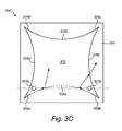
- FIG. 3 a wherein an embodiment of a lens antenna 300 according to preferred embodiments of the invention is shown.
- the antenna 300 comprises a ground plane 301 , an electromagnetic lens 302 mounted to said ground plane 301 , and a probing structure comprising two probes 303 a , 303 b .
- the lens 302 has a prismatic shape which complies with the superformula.
- the lens 302 is made of PVC in this example.
- the lens 302 is provided with an accommodating space 304 for accommodating the probe.
- the ground plane 301 is made of metal. Both the two probes 303 a and the ground plane 301 are connected, commonly via a control circuit (not shown), to an electrical power source, such as a battery (DC) or mains (AC).
- DC battery
- AC mains
- the lens 302 in this embodiment acts as dielectric resonator which makes the lens antenna 300 a dielectric resonator antenna (DRA). Since the lens 302 complies with the superformula, this antenna 300 can also be considered as a supershaped antenna (S-DRA).
- the circular metal plate acting as ground plane 301 has a radius plane.
- the antenna 300 is fed from the bottom side by means of a coaxial connector turning, at the ground plane level, into each electric probe 303 a of length h p and diameter d p .
- the probes 303 a , 303 b can have identical geometries, or can have different geometries. This latter option is commonly most favourable in case the lens antenna 300 should be configured as multiband antenna.
- the metal ground plane 301 has a radius ⁇ g and a thickness t g .
- the prismatic lens 302 had its axis aligned along the z-direction and its base profile defined by the polar function:
- ⁇ d ⁇ ( ⁇ ) [ ⁇ 1 a ⁇ cos ⁇ ( m 4 ⁇ ⁇ ) ⁇ n 2 + ⁇ 1 b ⁇ sin ⁇ ( m 4 ⁇ ⁇ ) ⁇ n 3 ] - 1 / n 1
- ⁇ d ( ⁇ ) is a curve located in the xy-plane and ⁇ [0, 2pi) is the angular coordinate.
- the polymeric lens 302 is provided with two accommodating spaces, each accommodated being configured to accommodate a single probe 303 a , 303 b in a well-fitting manner.
- the accommodating spaces, and therefore the probes 303 a , 303 b are positioned in or near different edges 304 a , 304 b of the lens 302 , as a result of which the probes 303 a , 303 b are positioned out of the line of sight (see the dashed line) of each other, which is further visualised in FIG. 3 a and FIG. 3 b .
- a circumferential wall 305 comprises four concave wall parts 305 a , 305 b , 305 c , 305 d connected to each other, as a result of which the aforementioned four corners 304 a , 304 b , 304 c , 304 d are defined.
- One of the concave wall parts 305 a is provided with a selective corrugated profile.
- Electromagnetic radiation excited by a probe 303 a , 303 b will be reflected (see arrows) by the wall parts 305 a , 305 b , 305 c , 305 d , and in particular by the intermediate corrugated wall parts 305 a , in a direction away from the other probe 303 b , 303 a so that mutual coupling and hence interference can be counteracted.
- PVC used for the lens 302 in this illustrative example is a thermoplastic polymer produced in enormous quantities in reason of low cost and ease of processing. Moreover, PVC is extremely durable and resistant to chemical corrosion and thus very well adapted to outdoor applications. Additionally, PVC can be blended with different materials providing a wide range of physical properties. The use of PVC can then result in an inexpensive option for manufacturing intricately shaped dielectric resonator/lens antennas by using conventional drilling/milling or more advanced three-dimensional printing techniques. This is furthermore of significant importance in order to enhance the aesthetic quality of the proposed radiating structures when used for wireless communications in habitable structures such as residential units, office buildings, theaters, stadiums, etc.
- three-dimensional solid objects are formed using an additive process in which successive layers of material are laid down one upon the other to create desired.
- plastics including bioplastics and combinations of plastics, depending on the dielectric constants of the material.
- various other materials can be employed to produce antennas in a highly sustainable way.
- antennas with dynamic shape changes to modify its behaviour for specific purposes using liquid components (such as liquid crystals) can be employed, with the dynamics of shape changes modified by mechanical or electronic steering, or making use of other physical forces.
- FIG. 4 shows a top view of a lens antenna 400 according to an embodiment of the invention, which is more or less similar to the antenna 300 as shown in FIGS. 3 a -3 c .
- the antenna 400 comprises a ground plane 401 , an electromagnetic lens 402 mounted to said ground plane 401 , and a probing structure comprising two probes 403 a , 403 b .
- the lens 402 has a prismatic shape which complies with the superformula, wherein a circumferential wall 404 is formed by four concave circumferential wall parts 404 a , 404 b , 404 c , 404 d , wherein adjacent wall parts 404 a , 404 b , 404 c , 404 d mutually form a sharp edge 405 a , 405 b , 405 c , 405 d of the lens 402 .
- Both probes 403 a , 403 b are positioned in different sharp edges 405 a , 405 b of the lens 402 .
- the probes 403 a , 403 do not see each other from an electromagnetic point of view.
- the direct line of sight (LOS) is roughly indicated by means of the horizontal dashed line LOS.
- the intermediate wall part 404 a is provided with a profiled surface, the electromagnetic radiation transmitted by a probe 403 a , 403 b will be reflected away from the other probe 403 a , 403 b (see arrows), which will reduce mutual coupling, and hence which will reduce interference within the lens antenna 400 , which will be in favour of the efficiency and capacity of the antenna 400 .
- a separate reflective element 406 (a mirror).
- This reflective element 406 can be formed by a metal plate, and is incorporated in the lens body 402 and is reflective on both sides such that electromagnetic radiation reaching the reflective element 406 will be reflected back, which may further reduce interference of radiation patterns transmitted by the different probes 403 a , 403 b respectively.
- the lens 402 is made of PVC in this example.
- the ground plane 401 is made of metal. Both the two probes 403 a , 403 b and the ground plane 401 are connected, commonly via a control circuit (not shown), to an electrical power source, such as a battery (DC) or mains (AC).
- DC battery
- AC mains
- the lens 402 in this embodiment acts as dielectric resonator which makes the lens antenna 400 a dielectric resonator antenna (DRA). Since the lens 402 complies with the superformula, this antenna 400 can also be considered as a supershaped antenna (S-DRA).
- the probes 403 a , 403 b can have identical geometries, or can have different geometries.
- FIG. 5 shows a top view of another embodiment of a lens antenna 500 according to the invention.
- the lens antenna comprises a metal ground plane 501 , an electromagnetic lens 502 mounted to said ground plane 501 , and a probing structure comprising five probes 503 a , 503 b , 503 c , 503 d , 503 e .
- the lens 502 has a prismatic shape and has a star shaped base profile 502 a complying with the aforementioned superformula.
- the probes 503 a , 503 b , 503 c , 503 d , 503 e are positioned, respectively, in different angular points (edges or corners) of the lens 502 .
- the different probes 503 a , 503 b , 503 , c , 503 d , 503 e will practically not see each other and will therefore not interfere with each other.
- the different probes 503 a , 503 b , 503 , c , 503 d , 503 e could have different geometry as to make the antenna 500 suitable for multiband operation, for example in Wi-Fi communication systems or in other communication systems.
- FIG. 6 shows a dual-band antenna 600 comprises a supershaped lens 601 enclosing two different probes 602 , 603 having mutually distinctive geometries, wherein the probes 602 , 603 are positioned out of the line of sight of each other.
- the lens 601 and the probes 602 , 603 are connected to a flat ground plane 604 .
- a flat ground plane 604 instead of a flat ground plane 604 also a curved or otherwise shaped ground plane 604 can be used.
- Each of the probes 602 , 603 extends from a coaxial connector 605 , 606 which connector is also connected to said ground plane 604 .
- the lens 601 is made of silicon in some examples.
- the shortest probe 602 is configured to operate within a frequency band of 2.4 GHz, while the longest probe 603 is configured to operate within a frequency band of 5 GHz, which makes this compact antenna 600 well suitable to serve as dual-band Wi-Fi-antenna.
- FIG. 7 shows a dual-band antenna 700 that comprises a lens 701 , and a reflective supershaped ground plane 702 connected to said lens 701 , wherein the ground plane 702 is provided with two central holes 703 a , 703 b , each hole 703 a , 703 b forming a slot or cavity between the lens 701 and a dielectric printed circuit board (PCB) 704 to which the ground plane 702 is attached.
- the holes 703 a , 703 b are positioned at least partially out of the line of sight of each other.
- a rear side of the PCB 704 is provided with two electrically conductive microstrips 705 a , 705 b .
- each microstrip 705 a , 705 b By connecting the ground plane 702 and each microstrip 705 a , 705 b to an electronic circuit 706 (schematically shown) including a power source, such as a battery, and commonly a control unit and a switch, a static planar wave front will be formed between each microstrip 705 a , 705 b and the ground plane 702 which will wave front will enter the lens 701 via each hole 703 a , 703 b and will turn into a spherical wave front within the lens 701 .
- the electromagnetic radiation within the lens 701 will be internally reflected and excited in a controlled manner, dependent on the (super)shape of the lens 701 and eventually the supershape of the ground plane 702 .
- This mechanism is also called a slot fed antenna.
- FIG. 8 shows a single-band antenna 800 that comprises a supershaped lens 801 , which lens 801 is connected to a laminate of an insulating layer 802 and an electrically conductive layer 803 acting as ground plane.
- the electrically conductive layer 803 provided with a central hole 804 through which two probes 805 a , 805 b extend.
- An outer end of each probe 805 a , 805 b is connected to a conductive patch 806 a , 806 b of similar geometry which are positioned within the lens 801 and which are configured to couple electromagnetic into and/or out of the lens 801 .
- the probes 805 a , 805 b are connected to control circuit 807 including a processor.
- Both the probes 805 a , 805 b and the electrically conductive layer 803 are connected to an AC power source 808 .
- the control circuit 807 is configured to be programmed by means of a computer interface 809 which allows a user to define the purpose of the antenna 800 (transmitting signals, receiving signals, or both) and further characteristics of the antenna 800 such as the frequency band which is used by the antenna 800 .
- FIG. 9 shows a multi-band antenna 900 that comprises a supershaped dielectric resonator 901 , which resonator 901 is connected to a laminate of a first insulating layer 902 , an electrically conductive layer 903 acting as ground plane, a second insulating layer 904 , and two microstrip 905 a . 905 b .
- the resonator 901 is made of PVC or Teflon® or a combination/mixture of polymer and ceramics.
- Within the resonator 901 and onto the first insulating layer 902 two electrically conductive patches 906 a , 906 b are provided.
- the patches 906 a , 906 b can either have a flat geometry or a supershaped geometry.
- the ground plane 903 is made of metal and/or an electrically conductive polymer and is provided with two holes 907 a , 907 b , and each microstrip 905 a , 905 b extends such that an outer end will be positioned in line with one of said patch 906 a , 906 b .
- the antenna 900 can make part of an electronic device 909 , such as e.g. a router, a notebook, or a mobile phone.
- FIG. 10 shows a MIMO-configured antenna system 1000 according to some embodiments of the invention, comprising multiple antennas 1001 , 1002 according to the invention, wherein said antennas 1001 , 1002 are configured to communicate with each other wirelessly in two directions.
- a first antenna 1001 comprises multiple probes 1003 , 1004 , 1005 , wherein two probes 1003 , 1004 have an identical geometry and are configured to operate within the same first frequency band, while the other probe 1005 , having a different geometry, is configured to operate within another second frequency band.
- the probes 1003 , 1004 , 1005 are enclosed by a supershaped lens 1006 which is supported by a ground plate 1007 .
- the probes make part of coaxial connectors 1008 , 1009 , 1010 which are connected to a control circuit (not shown). Use is made of two identical probes 1003 , 1004 , mutually positioned at sufficient distance from each other, in order to improve the communication and therefore reliability of this first antenna 1001 .
- the other antenna 1002 comprises two probes 1011 , 1012 , wherein a first probe 1011 is configured to operate within the first frequency band, and the other probe 1012 is configured to operate within the second frequency band.
- the probes 1011 , 1012 are enclosed by a supershaped lens 1013 which is supported by a ground plate (ground plane) 1014 .
- the probes make part of coaxial connectors 1015 , 1016 which are connected to a control circuit (not shown).
- inventive concepts are illustrated in a series of examples, some examples showing more than one inventive concept. Individual inventive concepts can be implemented without implementing all details provided in a particular example. It is not necessary to provide examples of every possible combination of the inventive concepts provide below as one of skill in the art will recognize that inventive concepts illustrated in various examples can be combined together in order to address a specific application.
- the terminology “present invention” or “invention” can be used as a reference to one or more aspect within the present disclosure.
- the language present invention or invention should not be improperly interpreted as an identification of criticality, should not be improperly interpreted as applying across all aspects or embodiments (i.e., it should be understood that the present invention has a number of aspects and embodiments), and should not be improperly interpreted as limiting the scope of the application or claims.
- the terminology “embodiment” can be used to describe any aspect, feature, process or step, any combination thereof, and/or any portion thereof, etc. In some examples, various embodiments can include overlapping features.
- abbreviated terminology can be employed: “e.g.” which means “for example.”
Landscapes
- Physics & Mathematics (AREA)
- Electromagnetism (AREA)
- Engineering & Computer Science (AREA)
- Computer Networks & Wireless Communication (AREA)
- Signal Processing (AREA)
- Aerials With Secondary Devices (AREA)
- Variable-Direction Aerials And Aerial Arrays (AREA)
- Transceivers (AREA)
- Control Of Motors That Do Not Use Commutators (AREA)
- Support Of Aerials (AREA)
Priority Applications (1)
| Application Number | Priority Date | Filing Date | Title |
|---|---|---|---|
| US14/429,731 US9716319B2 (en) | 2012-09-24 | 2013-03-15 | Lens antenna, method for manufacturing and using such an antenna, and antenna system |
Applications Claiming Priority (3)
| Application Number | Priority Date | Filing Date | Title |
|---|---|---|---|
| US201261705117P | 2012-09-24 | 2012-09-24 | |
| US14/429,731 US9716319B2 (en) | 2012-09-24 | 2013-03-15 | Lens antenna, method for manufacturing and using such an antenna, and antenna system |
| PCT/NL2013/050195 WO2014046538A1 (en) | 2012-09-24 | 2013-03-15 | Lens antenna, method of manufacturing and using such an antenna, and antenna system |
Publications (2)
| Publication Number | Publication Date |
|---|---|
| US20150236428A1 US20150236428A1 (en) | 2015-08-20 |
| US9716319B2 true US9716319B2 (en) | 2017-07-25 |
Family
ID=47997741
Family Applications (2)
| Application Number | Title | Priority Date | Filing Date |
|---|---|---|---|
| US14/429,731 Active 2033-09-03 US9716319B2 (en) | 2012-09-24 | 2013-03-15 | Lens antenna, method for manufacturing and using such an antenna, and antenna system |
| US14/429,732 Active 2033-04-19 US9831562B2 (en) | 2012-09-24 | 2013-03-15 | Lens antenna, method for manufacturing and using such an antenna, and antenna system |
Family Applications After (1)
| Application Number | Title | Priority Date | Filing Date |
|---|---|---|---|
| US14/429,732 Active 2033-04-19 US9831562B2 (en) | 2012-09-24 | 2013-03-15 | Lens antenna, method for manufacturing and using such an antenna, and antenna system |
Country Status (12)
| Country | Link |
|---|---|
| US (2) | US9716319B2 (enExample) |
| EP (4) | EP2896090B1 (enExample) |
| JP (2) | JP6001181B2 (enExample) |
| KR (2) | KR101697032B1 (enExample) |
| CN (2) | CN104956545B (enExample) |
| AU (2) | AU2013318708A1 (enExample) |
| BR (2) | BR112015006449A2 (enExample) |
| CA (2) | CA2885890A1 (enExample) |
| IL (2) | IL237851A0 (enExample) |
| RU (2) | RU2622467C2 (enExample) |
| WO (2) | WO2014046538A1 (enExample) |
| ZA (2) | ZA201502543B (enExample) |
Cited By (5)
| Publication number | Priority date | Publication date | Assignee | Title |
|---|---|---|---|---|
| US20190103660A1 (en) * | 2017-09-29 | 2019-04-04 | Commscope Technologies Llc | Base station antennas with lenses for reducing upwardly-directed radiation |
| EP4194904A1 (en) * | 2021-12-09 | 2023-06-14 | Canon Kabushiki Kaisha | Radiation detection apparatus |
| US11804652B2 (en) | 2019-06-25 | 2023-10-31 | Nokia Solutions And Networks Oy | Antenna having controlled directivity |
| US20240039167A1 (en) * | 2021-06-16 | 2024-02-01 | Qualcomm Incorporated | Lens communication with multiple antenna arrays |
| US12206176B2 (en) | 2021-04-20 | 2025-01-21 | Apple Inc. | Electronic devices having bi-directional dielectric resonator antennas |
Families Citing this family (69)
| Publication number | Priority date | Publication date | Assignee | Title |
|---|---|---|---|---|
| WO2016005909A1 (en) * | 2014-07-07 | 2016-01-14 | University Of Manitoba | Imaging using reconfigurable antennas |
| EP3198680B1 (en) | 2014-09-24 | 2021-05-05 | The Antenna Company International N.V. | Blade antenna and wireless local area network comprising a blade antenna |
| US10547118B2 (en) * | 2015-01-27 | 2020-01-28 | Huawei Technologies Co., Ltd. | Dielectric resonator antenna arrays |
| CN104953281B (zh) * | 2015-05-27 | 2017-07-11 | 华中科技大学 | 一种频率可调的介质谐振器天线 |
| US10601137B2 (en) | 2015-10-28 | 2020-03-24 | Rogers Corporation | Broadband multiple layer dielectric resonator antenna and method of making the same |
| US11367959B2 (en) | 2015-10-28 | 2022-06-21 | Rogers Corporation | Broadband multiple layer dielectric resonator antenna and method of making the same |
| US10355361B2 (en) | 2015-10-28 | 2019-07-16 | Rogers Corporation | Dielectric resonator antenna and method of making the same |
| US10374315B2 (en) | 2015-10-28 | 2019-08-06 | Rogers Corporation | Broadband multiple layer dielectric resonator antenna and method of making the same |
| US10476164B2 (en) | 2015-10-28 | 2019-11-12 | Rogers Corporation | Broadband multiple layer dielectric resonator antenna and method of making the same |
| KR20170112715A (ko) * | 2016-04-01 | 2017-10-12 | 삼성전자주식회사 | 안테나 장치 및 그것을 포함하는 전자 장치 |
| CN106058447B (zh) * | 2016-05-16 | 2019-02-15 | 电子科技大学 | 一种适用于x波段的宽带宽波束圆极化介质谐振器天线 |
| TWI629835B (zh) * | 2016-07-21 | 2018-07-11 | 和碩聯合科技股份有限公司 | 天線單元、天線系統及天線控制方法 |
| CN112886216B (zh) * | 2016-10-21 | 2024-02-13 | 株式会社友华 | 车载天线装置及天线系统 |
| US10116051B2 (en) * | 2017-03-17 | 2018-10-30 | Isotropic Systems Ltd. | Lens antenna system |
| US11283189B2 (en) | 2017-05-02 | 2022-03-22 | Rogers Corporation | Connected dielectric resonator antenna array and method of making the same |
| US11876295B2 (en) | 2017-05-02 | 2024-01-16 | Rogers Corporation | Electromagnetic reflector for use in a dielectric resonator antenna system |
| KR102312067B1 (ko) | 2017-06-07 | 2021-10-13 | 로저스코포레이션 | 유전체 공진기 안테나 시스템 |
| WO2018224617A1 (en) * | 2017-06-09 | 2018-12-13 | Essilor International | Method and system for manufacturing an optical lens having an electronic component |
| KR101894840B1 (ko) | 2017-09-15 | 2018-09-04 | 세종대학교산학협력단 | 알에프 렌즈 및 이를 포함하는 안테나 |
| US10923818B2 (en) * | 2017-09-21 | 2021-02-16 | City University Of Hong Kong | Dual-fed dual-frequency hollow dielectric antenna |
| US20220190464A1 (en) * | 2017-10-06 | 2022-06-16 | At&S Austria Technologie & Systemtechnik Aktiengesellschaft | Component Carrier Having at Least a Part Formed as a Three-Dimensionally Printed Structure Forming an Antenna |
| US20190115668A1 (en) * | 2017-10-13 | 2019-04-18 | ETS-Lindgren Inc. | Rf lens and method of manufacture |
| RU2681276C1 (ru) * | 2017-12-19 | 2019-03-05 | Закрытое акционерное общество "Научно-производственное предприятие оборудования систем телекоммуникаций" | Панельная антенна |
| JP6633604B2 (ja) * | 2017-12-21 | 2020-01-22 | アンリツ株式会社 | アンテナ測定システム及びアンテナ測定方法 |
| US10892544B2 (en) | 2018-01-15 | 2021-01-12 | Rogers Corporation | Dielectric resonator antenna having first and second dielectric portions |
| US11616302B2 (en) | 2018-01-15 | 2023-03-28 | Rogers Corporation | Dielectric resonator antenna having first and second dielectric portions |
| US10910722B2 (en) | 2018-01-15 | 2021-02-02 | Rogers Corporation | Dielectric resonator antenna having first and second dielectric portions |
| KR102104483B1 (ko) * | 2018-01-30 | 2020-04-24 | 한국과학기술원 | 패턴 구성 제어가 가능한 유전체 공진기 안테나 |
| KR102437420B1 (ko) * | 2018-03-02 | 2022-08-29 | 옵티시스, 엘엘씨 | 금속 적층 제조를 이용한 안테나 조립체의 대량 맞춤화 |
| CN108933334B (zh) * | 2018-07-19 | 2021-04-02 | 华北水利水电大学 | 一种球体龙勃电磁透镜反射器的制作方法及装置 |
| US11552390B2 (en) | 2018-09-11 | 2023-01-10 | Rogers Corporation | Dielectric resonator antenna system |
| TWI820237B (zh) | 2018-10-18 | 2023-11-01 | 美商羅傑斯公司 | 聚合物結構、其立體光刻製造方法以及包含該聚合物結構之電子裝置 |
| US11031697B2 (en) | 2018-11-29 | 2021-06-08 | Rogers Corporation | Electromagnetic device |
| US11637377B2 (en) | 2018-12-04 | 2023-04-25 | Rogers Corporation | Dielectric electromagnetic structure and method of making the same |
| CN111509403B (zh) * | 2019-01-31 | 2022-02-18 | Oppo广东移动通信有限公司 | 阵列天线和电子设备 |
| US10886617B2 (en) | 2019-02-28 | 2021-01-05 | Apple Inc. | Electronic devices with probe-fed dielectric resonator antennas |
| US10886619B2 (en) | 2019-02-28 | 2021-01-05 | Apple Inc. | Electronic devices with dielectric resonator antennas |
| EP3918362B1 (en) * | 2019-04-04 | 2024-10-23 | Siemens Industry Software NV | A method for computer-implemented simulation of radar raw data |
| US10833415B2 (en) | 2019-04-11 | 2020-11-10 | The Boeing Company | Radio frequency circuit board with microstrip-to-waveguide transition |
| RU2715914C1 (ru) * | 2019-05-29 | 2020-03-04 | Федеральное Государственное Бюджетное Образовательное Учреждение Высшего Образования "Новосибирский Государственный Технический Университет" | Способ определения поверхности диэлектрической бифокальной линзовой антенны |
| US10903540B2 (en) | 2019-05-31 | 2021-01-26 | Nokia Solutions And Networks Oy | Dual-mode corrugated waveguide cavity filter |
| CN110414164B (zh) * | 2019-08-01 | 2020-12-08 | 西安电子科技大学 | 一种基于机电耦合的6g通信天线信道容量预测方法 |
| CN110707432B (zh) * | 2019-09-18 | 2021-01-08 | 佛山市粤海信通讯有限公司 | 发泡介质材料及发泡介质材料生产方法 |
| US11239566B2 (en) * | 2019-09-26 | 2022-02-01 | Corning Incorporated | Fresnel phase lenses for 5G applications |
| KR102090767B1 (ko) * | 2019-10-04 | 2020-05-26 | (주)디 넷 | 센서용 레이더 모듈 장치 |
| US11550062B2 (en) | 2019-12-24 | 2023-01-10 | All.Space Networks Ltd. | High-gain multibeam GNSS antenna |
| CN110783713B (zh) * | 2019-12-31 | 2020-11-24 | 佛山市粤海信通讯有限公司 | 一种电磁波透镜及天线及天线阵列 |
| US11482790B2 (en) | 2020-04-08 | 2022-10-25 | Rogers Corporation | Dielectric lens and electromagnetic device with same |
| US12155134B2 (en) | 2020-04-17 | 2024-11-26 | Apple Inc. | Electronic devices having dielectric resonator antennas with parasitic patches |
| US11177548B1 (en) | 2020-05-04 | 2021-11-16 | The Boeing Company | Electromagnetic wave concentration |
| CN111613879B (zh) * | 2020-06-09 | 2021-09-21 | 四川大学 | 一种介质非谐振天线 |
| TWI888303B (zh) * | 2020-06-20 | 2025-06-21 | 愛爾蘭商陶格拉斯集團控股有限公司 | 天線裝置 |
| US11967781B2 (en) * | 2020-09-23 | 2024-04-23 | Apple Inc. | Electronic devices having compact dielectric resonator antennas |
| US12183963B2 (en) | 2020-10-19 | 2024-12-31 | Optisys, Inc. | Device comprising a transition between a waveguide port and two or more coaxial waveguides |
| CN114389018B (zh) * | 2020-10-22 | 2023-01-31 | 展讯通信(上海)有限公司 | 贴片天线单元以及封装天线阵列 |
| WO2022094325A1 (en) | 2020-10-29 | 2022-05-05 | Optisys, Inc. | Integrated balanced radiating elements |
| CN112272146A (zh) * | 2020-11-12 | 2021-01-26 | 佛山蓝谱达科技有限公司 | 一种无线传输速率高的毫米波路由器 |
| CN112269265A (zh) * | 2020-11-12 | 2021-01-26 | 佛山蓝谱达科技有限公司 | 一种具有高速无线传输功能的vr设备 |
| KR20220068511A (ko) * | 2020-11-19 | 2022-05-26 | 삼성전기주식회사 | 안테나 장치 |
| US12119554B2 (en) | 2021-05-14 | 2024-10-15 | Optisys, Inc. | Planar monolithic combiner and multiplexer for antenna arrays |
| US12355158B1 (en) | 2021-07-08 | 2025-07-08 | Lockheed Martin Corporation | Vivaldi antenna structures with concurrent transmit and receive |
| US12148999B1 (en) | 2021-07-08 | 2024-11-19 | Lockheed Martin Corporation | Multimode vivaldi antenna structures |
| RU2770237C1 (ru) * | 2021-09-03 | 2022-04-14 | федеральное государственное автономное образовательное учреждение высшего образования «Московский физико-технический институт (национальный исследовательский университет)» | Устройство приёмопередающее и способ его изготовления |
| CN114566800B (zh) * | 2022-02-14 | 2024-12-17 | 中山大学 | 基于方向图解耦的mimo介质谐振器天线 |
| US11936112B1 (en) | 2022-05-05 | 2024-03-19 | Lockheed Martin Corporation | Aperture antenna structures with concurrent transmit and receive |
| US20240080678A1 (en) * | 2022-08-25 | 2024-03-07 | Rosemount Inc. | Wireless industrial process field device having a plurality of transceivers |
| CN115732938A (zh) * | 2022-10-21 | 2023-03-03 | 深圳科瑞沃科技有限公司 | 一种低介电微波透明透镜及天线 |
| CN120731540A (zh) * | 2023-03-15 | 2025-09-30 | 户外无线网络有限公司 | 每频段波束的数目与频段之间的频率比无关的带透镜的扇区分裂多频段基站天线 |
| CN119651198A (zh) * | 2024-11-13 | 2025-03-18 | 广州大学 | 一种3d打印的透明多波束毫米波天线 |
Citations (8)
| Publication number | Priority date | Publication date | Assignee | Title |
|---|---|---|---|---|
| US6452565B1 (en) | 1999-10-29 | 2002-09-17 | Antenova Limited | Steerable-beam multiple-feed dielectric resonator antenna |
| WO2004088793A1 (en) | 2003-03-31 | 2004-10-14 | Bae Systems Plc | Low-profile lens antenna |
| US20050068251A1 (en) | 1999-11-18 | 2005-03-31 | Automotive Systems Laboratory, Inc. | Multi-beam antenna |
| EP1536517A1 (en) | 2003-11-28 | 2005-06-01 | Kabushiki Kaisha Toshiba | Lens antenna apparatus |
| WO2005093905A1 (en) | 2004-03-26 | 2005-10-06 | Bae Systems Plc | An antenna with partially spherical dielectric lenses |
| US7570219B1 (en) | 2006-05-16 | 2009-08-04 | Rockwell Collins, Inc. | Circular polarization antenna for precision guided munitions |
| US20100220031A1 (en) | 2006-12-04 | 2010-09-02 | Agc Automotive Americas R&D, Inc. | Wideband dielectric antenna |
| WO2011161548A2 (en) | 2010-06-21 | 2011-12-29 | Johan Gielis | Computer implemented tool box systems and methods |
Family Cites Families (37)
| Publication number | Priority date | Publication date | Assignee | Title |
|---|---|---|---|---|
| JPS6074003A (ja) | 1983-09-30 | 1985-04-26 | Ryozo Setoguchi | 形状創成装置 |
| US5236637A (en) | 1984-08-08 | 1993-08-17 | 3D Systems, Inc. | Method of and apparatus for production of three dimensional objects by stereolithography |
| US4942001A (en) | 1988-03-02 | 1990-07-17 | Inc. DeSoto | Method of forming a three-dimensional object by stereolithography and composition therefore |
| US5184307A (en) | 1988-04-18 | 1993-02-02 | 3D Systems, Inc. | Method and apparatus for production of high resolution three-dimensional objects by stereolithography |
| US5182056A (en) | 1988-04-18 | 1993-01-26 | 3D Systems, Inc. | Stereolithography method and apparatus employing various penetration depths |
| US5059359A (en) | 1988-04-18 | 1991-10-22 | 3 D Systems, Inc. | Methods and apparatus for production of three-dimensional objects by stereolithography |
| US5256340A (en) | 1988-04-18 | 1993-10-26 | 3D Systems, Inc. | Method of making a three-dimensional object by stereolithography |
| US5130064A (en) | 1988-04-18 | 1992-07-14 | 3D Systems, Inc. | Method of making a three dimensional object by stereolithography |
| US5182055A (en) | 1988-04-18 | 1993-01-26 | 3D Systems, Inc. | Method of making a three-dimensional object by stereolithography |
| US5609813A (en) | 1988-04-18 | 1997-03-11 | 3D Systems, Inc. | Method of making a three-dimensional object by stereolithography |
| US4844144A (en) | 1988-08-08 | 1989-07-04 | Desoto, Inc. | Investment casting utilizing patterns produced by stereolithography |
| US5143663A (en) | 1989-06-12 | 1992-09-01 | 3D Systems, Inc. | Stereolithography method and apparatus |
| EP0405106A3 (en) | 1989-06-16 | 1992-04-08 | International Business Machines Corporation | Construction of minkowski sums and derivative morphological combinations of arbitrary polyhedra in cad/cam systems |
| US5182715A (en) | 1989-10-27 | 1993-01-26 | 3D Systems, Inc. | Rapid and accurate production of stereolighographic parts |
| US5167882A (en) | 1990-12-21 | 1992-12-01 | Loctite Corporation | Stereolithography method |
| US5217653A (en) | 1991-02-18 | 1993-06-08 | Leonid Mashinsky | Method and apparatus for producing a stepless 3-dimensional object by stereolithography |
| US5247180A (en) | 1991-12-30 | 1993-09-21 | Texas Instruments Incorporated | Stereolithographic apparatus and method of use |
| JP2558431B2 (ja) | 1993-01-15 | 1996-11-27 | ストラタシイス,インコーポレイテッド | 3次元構造体を製造するシステムを作動する方法及び3次元構造体製造装置 |
| US5296335A (en) | 1993-02-22 | 1994-03-22 | E-Systems, Inc. | Method for manufacturing fiber-reinforced parts utilizing stereolithography tooling |
| SE501411C2 (sv) | 1993-07-12 | 1995-02-06 | Nobelpharma Ab | Förfarande och anordning vid tredimensionell kropp användbar i människokroppen |
| US5458825A (en) | 1993-08-12 | 1995-10-17 | Hoover Universal, Inc. | Utilization of blow molding tooling manufactured by sterolithography for rapid container prototyping |
| US5398193B1 (en) | 1993-08-20 | 1997-09-16 | Alfredo O Deangelis | Method of three-dimensional rapid prototyping through controlled layerwise deposition/extraction and apparatus therefor |
| US5491643A (en) | 1994-02-04 | 1996-02-13 | Stratasys, Inc. | Method for optimizing parameters characteristic of an object developed in a rapid prototyping system |
| US5796620A (en) | 1995-02-03 | 1998-08-18 | Cleveland Advanced Manufacturing Program | Computerized system for lost foam casting process using rapid tooling set-up |
| US5547305A (en) | 1995-03-02 | 1996-08-20 | The Whitaker Corporation | Rapid, tool-less adjusting system for hotstick tooling |
| US5728345A (en) | 1995-03-03 | 1998-03-17 | General Motors Corporation | Method for making an electrode for electrical discharge machining by use of a stereolithography model |
| US5616293A (en) | 1995-03-03 | 1997-04-01 | General Motors Corporation | Rapid making of a prototype part or mold using stereolithography model |
| US5639413A (en) | 1995-03-30 | 1997-06-17 | Crivello; James Vincent | Methods and compositions related to stereolithography |
| WO1996036921A1 (en) | 1995-05-19 | 1996-11-21 | 3Com Corporation | Method and apparatus for linking computer aided design databases with a numerical control machine database |
| US5663883A (en) | 1995-08-21 | 1997-09-02 | University Of Utah Research Foundation | Rapid prototyping method |
| US5622577A (en) | 1995-08-28 | 1997-04-22 | Delco Electronics Corp. | Rapid prototyping process and cooling chamber therefor |
| US5818718A (en) | 1996-04-01 | 1998-10-06 | University Of Utah Research Foundation | Higher order construction algorithm method for rapid prototyping |
| US5578227A (en) | 1996-11-22 | 1996-11-26 | Rabinovich; Joshua E. | Rapid prototyping system |
| US5846370A (en) | 1997-03-17 | 1998-12-08 | Delco Electronics Corporation | Rapid prototyping process and apparatus therefor |
| US6147647A (en) * | 1998-09-09 | 2000-11-14 | Qualcomm Incorporated | Circularly polarized dielectric resonator antenna |
| US7620527B1 (en) | 1999-05-10 | 2009-11-17 | Johan Leo Alfons Gielis | Method and apparatus for synthesizing and analyzing patterns utilizing novel “super-formula” operator |
| US6861989B2 (en) * | 2003-07-03 | 2005-03-01 | Motorola, Inc. | Antenna system for a communication device |
-
2013
- 2013-03-15 CA CA2885890A patent/CA2885890A1/en not_active Abandoned
- 2013-03-15 AU AU2013318708A patent/AU2013318708A1/en not_active Abandoned
- 2013-03-15 EP EP13712385.7A patent/EP2896090B1/en active Active
- 2013-03-15 BR BR112015006449A patent/BR112015006449A2/pt not_active IP Right Cessation
- 2013-03-15 WO PCT/NL2013/050195 patent/WO2014046538A1/en not_active Ceased
- 2013-03-15 JP JP2015533004A patent/JP6001181B2/ja not_active Expired - Fee Related
- 2013-03-15 RU RU2015115282A patent/RU2622467C2/ru active
- 2013-03-15 AU AU2013318709A patent/AU2013318709A1/en not_active Abandoned
- 2013-03-15 RU RU2015115283A patent/RU2622463C2/ru active
- 2013-03-15 EP EP16159038.5A patent/EP3062395A1/en not_active Withdrawn
- 2013-03-15 US US14/429,731 patent/US9716319B2/en active Active
- 2013-03-15 JP JP2015533003A patent/JP6001180B2/ja not_active Expired - Fee Related
- 2013-03-15 KR KR1020157010808A patent/KR101697032B1/ko not_active Expired - Fee Related
- 2013-03-15 CA CA2885954A patent/CA2885954A1/en not_active Abandoned
- 2013-03-15 KR KR1020157010812A patent/KR101697033B1/ko not_active Expired - Fee Related
- 2013-03-15 WO PCT/NL2013/050194 patent/WO2014046537A1/en not_active Ceased
- 2013-03-15 CN CN201380059320.8A patent/CN104956545B/zh not_active Expired - Fee Related
- 2013-03-15 CN CN201380059327.XA patent/CN104781987A/zh active Pending
- 2013-03-15 EP EP16174770.4A patent/EP3093921A1/en not_active Withdrawn
- 2013-03-15 EP EP13712384.0A patent/EP2896089B1/en active Active
- 2013-03-15 BR BR112015006447A patent/BR112015006447A2/pt not_active IP Right Cessation
- 2013-03-15 US US14/429,732 patent/US9831562B2/en active Active
-
2015
- 2015-03-19 IL IL237851A patent/IL237851A0/en unknown
- 2015-03-19 IL IL237850A patent/IL237850A0/en unknown
- 2015-04-15 ZA ZA2015/02543A patent/ZA201502543B/en unknown
- 2015-04-15 ZA ZA2015/02544A patent/ZA201502544B/en unknown
Patent Citations (10)
| Publication number | Priority date | Publication date | Assignee | Title |
|---|---|---|---|---|
| US6452565B1 (en) | 1999-10-29 | 2002-09-17 | Antenova Limited | Steerable-beam multiple-feed dielectric resonator antenna |
| US20050068251A1 (en) | 1999-11-18 | 2005-03-31 | Automotive Systems Laboratory, Inc. | Multi-beam antenna |
| WO2004088793A1 (en) | 2003-03-31 | 2004-10-14 | Bae Systems Plc | Low-profile lens antenna |
| EP1536517A1 (en) | 2003-11-28 | 2005-06-01 | Kabushiki Kaisha Toshiba | Lens antenna apparatus |
| WO2005093905A1 (en) | 2004-03-26 | 2005-10-06 | Bae Systems Plc | An antenna with partially spherical dielectric lenses |
| US7570219B1 (en) | 2006-05-16 | 2009-08-04 | Rockwell Collins, Inc. | Circular polarization antenna for precision guided munitions |
| US20100220031A1 (en) | 2006-12-04 | 2010-09-02 | Agc Automotive Americas R&D, Inc. | Wideband dielectric antenna |
| US8009107B2 (en) * | 2006-12-04 | 2011-08-30 | Agc Automotive Americas R&D, Inc. | Wideband dielectric antenna |
| WO2011161548A2 (en) | 2010-06-21 | 2011-12-29 | Johan Gielis | Computer implemented tool box systems and methods |
| US8818771B2 (en) | 2010-06-21 | 2014-08-26 | Johan Gielis | Computer implemented tool box systems and methods |
Non-Patent Citations (2)
| Title |
|---|
| Kishk et al., Broadband dielectric resonator antennas excited by L-shaped probe, IEEE Transactions on Antennas and Propagation (Aug. 2006), 54(8): 2182-2189. |
| Simeoni, et al., "Plastic-Based Supershaped Dielectric Resonator Antennas for Wide-Band Applications", IEEE Transactions on Antennas and Propagation, 2011, 59(12): 4820-4825. |
Cited By (8)
| Publication number | Priority date | Publication date | Assignee | Title |
|---|---|---|---|---|
| US20190103660A1 (en) * | 2017-09-29 | 2019-04-04 | Commscope Technologies Llc | Base station antennas with lenses for reducing upwardly-directed radiation |
| US10587034B2 (en) * | 2017-09-29 | 2020-03-10 | Commscope Technologies Llc | Base station antennas with lenses for reducing upwardly-directed radiation |
| US11804652B2 (en) | 2019-06-25 | 2023-10-31 | Nokia Solutions And Networks Oy | Antenna having controlled directivity |
| US12206176B2 (en) | 2021-04-20 | 2025-01-21 | Apple Inc. | Electronic devices having bi-directional dielectric resonator antennas |
| US20240039167A1 (en) * | 2021-06-16 | 2024-02-01 | Qualcomm Incorporated | Lens communication with multiple antenna arrays |
| US12388187B2 (en) * | 2021-06-16 | 2025-08-12 | Qualcomm Incorporated | Lens communication with multiple antenna arrays |
| EP4194904A1 (en) * | 2021-12-09 | 2023-06-14 | Canon Kabushiki Kaisha | Radiation detection apparatus |
| US12207964B2 (en) | 2021-12-09 | 2025-01-28 | Canon Kabushiki Kaisha | Radiation detection apparatus |
Also Published As
Similar Documents
| Publication | Publication Date | Title |
|---|---|---|
| US9716319B2 (en) | Lens antenna, method for manufacturing and using such an antenna, and antenna system | |
| US10128572B2 (en) | Patch antenna, method of manufacturing and using such an antenna, and antenna system | |
| Fuchs et al. | Off-axis performances of half Maxwell fish-eye lens antennas at 77 GHz | |
| Miao | Ka-band 2D Luneburg lens design with glide-symmetric metasurface | |
| Abar | Antenna System Design for 5G and Beyond–A Modal Approach | |
| Magri et al. | Pattern for Miniaturized Arrays | |
| Ali et al. | Design and Implementation of A 6G-Ready Antenna System For High-Frequency Communication | |
| Bergman | Surface-mountable dual-polarized antenna arrays for 100 GHz | |
| Shukla | Design of Microstrip antenna for wireless applications | |
| Mishra et al. | Historical Review of DRA to MIMO-DRADesigns and Advances | |
| Khattak et al. | Design and Simulation of Microstrip Phase Array Antenna using ADS | |
| Mishra et al. | 8 Historical Review of | |
| OGADI | DESIGN AND CONSTRUCTION OF A RECTANGULAR MICROSTRIP PATCH ANTENNA | |
| Siddique | Design and Simulation of Microstrip Phase Array Antenna using ADS | |
| Moreno Laparte | On the analysis and design of 5G antenna arrays | |
| Ashmore | Design and Analysis of a Cylindrical Dielectric Resonator Antenna Array and Its Feed Network |
Legal Events
| Date | Code | Title | Description |
|---|---|---|---|
| AS | Assignment |
Owner name: THE ANTENNA COMPANY INTERNATIONAL N.V., CURACAO Free format text: ASSIGNMENT OF ASSIGNORS INTEREST;ASSIGNORS:CARATELLI, DIEGO;GIELIS, JOHAN LEO ALFONS;REEL/FRAME:035389/0547 Effective date: 20150401 |
|
| STCF | Information on status: patent grant |
Free format text: PATENTED CASE |
|
| CC | Certificate of correction | ||
| MAFP | Maintenance fee payment |
Free format text: PAYMENT OF MAINTENANCE FEE, 4TH YEAR, LARGE ENTITY (ORIGINAL EVENT CODE: M1551); ENTITY STATUS OF PATENT OWNER: LARGE ENTITY Year of fee payment: 4 |
|
| MAFP | Maintenance fee payment |
Free format text: PAYMENT OF MAINTENANCE FEE, 8TH YEAR, LARGE ENTITY (ORIGINAL EVENT CODE: M1552); ENTITY STATUS OF PATENT OWNER: LARGE ENTITY Year of fee payment: 8 |