US9709710B2 - Device including light blocking layer and method of patterning the light blocking layer - Google Patents
Device including light blocking layer and method of patterning the light blocking layer Download PDFInfo
- Publication number
- US9709710B2 US9709710B2 US14/940,337 US201514940337A US9709710B2 US 9709710 B2 US9709710 B2 US 9709710B2 US 201514940337 A US201514940337 A US 201514940337A US 9709710 B2 US9709710 B2 US 9709710B2
- Authority
- US
- United States
- Prior art keywords
- light blocking
- weight
- blocking layer
- group
- parts
- Prior art date
- Legal status (The legal status is an assumption and is not a legal conclusion. Google has not performed a legal analysis and makes no representation as to the accuracy of the status listed.)
- Active
Links
- 230000000903 blocking effect Effects 0.000 title claims abstract description 76
- 238000000034 method Methods 0.000 title claims abstract description 61
- 238000000059 patterning Methods 0.000 title claims abstract description 39
- 239000000203 mixture Substances 0.000 claims abstract description 82
- 239000003431 cross linking reagent Substances 0.000 claims abstract description 34
- 239000010408 film Substances 0.000 claims abstract description 29
- 239000003086 colorant Substances 0.000 claims abstract description 28
- 229920000642 polymer Polymers 0.000 claims abstract description 28
- 238000002161 passivation Methods 0.000 claims abstract description 23
- 239000000758 substrate Substances 0.000 claims abstract description 22
- 239000002904 solvent Substances 0.000 claims abstract description 20
- 239000010409 thin film Substances 0.000 claims abstract description 11
- 238000009413 insulation Methods 0.000 claims abstract description 5
- 239000000126 substance Substances 0.000 claims description 58
- 230000008569 process Effects 0.000 claims description 35
- 239000003795 chemical substances by application Substances 0.000 claims description 34
- 229920005989 resin Polymers 0.000 claims description 19
- 239000011347 resin Substances 0.000 claims description 19
- 238000010438 heat treatment Methods 0.000 claims description 18
- 238000005530 etching Methods 0.000 claims description 17
- SECXISVLQFMRJM-UHFFFAOYSA-N N-Methylpyrrolidone Chemical compound CN1CCCC1=O SECXISVLQFMRJM-UHFFFAOYSA-N 0.000 claims description 16
- 229920002120 photoresistant polymer Polymers 0.000 claims description 16
- 239000002243 precursor Substances 0.000 claims description 16
- IAZDPXIOMUYVGZ-UHFFFAOYSA-N Dimethylsulphoxide Chemical compound CS(C)=O IAZDPXIOMUYVGZ-UHFFFAOYSA-N 0.000 claims description 14
- WGTYBPLFGIVFAS-UHFFFAOYSA-M tetramethylammonium hydroxide Chemical compound [OH-].C[N+](C)(C)C WGTYBPLFGIVFAS-UHFFFAOYSA-M 0.000 claims description 14
- 125000000524 functional group Chemical group 0.000 claims description 13
- 125000004435 hydrogen atom Chemical group [H]* 0.000 claims description 13
- GHPVDCPCKSNJDR-UHFFFAOYSA-N 2-hydroxydecanoic acid Chemical compound CCCCCCCCC(O)C(O)=O GHPVDCPCKSNJDR-UHFFFAOYSA-N 0.000 claims description 12
- LZCLXQDLBQLTDK-UHFFFAOYSA-N ethyl 2-hydroxypropanoate Chemical compound CCOC(=O)C(C)O LZCLXQDLBQLTDK-UHFFFAOYSA-N 0.000 claims description 12
- OFOBLEOULBTSOW-UHFFFAOYSA-N Malonic acid Chemical compound OC(=O)CC(O)=O OFOBLEOULBTSOW-UHFFFAOYSA-N 0.000 claims description 11
- 239000011248 coating agent Substances 0.000 claims description 11
- 238000000576 coating method Methods 0.000 claims description 11
- ARXJGSRGQADJSQ-UHFFFAOYSA-N 1-methoxypropan-2-ol Chemical compound COCC(C)O ARXJGSRGQADJSQ-UHFFFAOYSA-N 0.000 claims description 10
- IISBACLAFKSPIT-UHFFFAOYSA-N bisphenol A Chemical compound C=1C=C(O)C=CC=1C(C)(C)C1=CC=C(O)C=C1 IISBACLAFKSPIT-UHFFFAOYSA-N 0.000 claims description 10
- PXKLMJQFEQBVLD-UHFFFAOYSA-N bisphenol F Chemical compound C1=CC(O)=CC=C1CC1=CC=C(O)C=C1 PXKLMJQFEQBVLD-UHFFFAOYSA-N 0.000 claims description 10
- 239000006229 carbon black Substances 0.000 claims description 10
- 239000004094 surface-active agent Substances 0.000 claims description 10
- 125000000008 (C1-C10) alkyl group Chemical group 0.000 claims description 9
- 238000011161 development Methods 0.000 claims description 9
- 229920002577 polybenzoxazole Polymers 0.000 claims description 9
- 239000004642 Polyimide Substances 0.000 claims description 7
- 238000004061 bleaching Methods 0.000 claims description 7
- 229910052731 fluorine Inorganic materials 0.000 claims description 7
- 229920003986 novolac Polymers 0.000 claims description 7
- 229920001721 polyimide Polymers 0.000 claims description 7
- LLHKCFNBLRBOGN-UHFFFAOYSA-N propylene glycol methyl ether acetate Chemical compound COCC(C)OC(C)=O LLHKCFNBLRBOGN-UHFFFAOYSA-N 0.000 claims description 7
- 125000006832 (C1-C10) alkylene group Chemical group 0.000 claims description 6
- OAYXUHPQHDHDDZ-UHFFFAOYSA-N 2-(2-butoxyethoxy)ethanol Chemical compound CCCCOCCOCCO OAYXUHPQHDHDDZ-UHFFFAOYSA-N 0.000 claims description 6
- HZAXFHJVJLSVMW-UHFFFAOYSA-N 2-Aminoethan-1-ol Chemical compound NCCO HZAXFHJVJLSVMW-UHFFFAOYSA-N 0.000 claims description 6
- YCKRFDGAMUMZLT-UHFFFAOYSA-N Fluorine atom Chemical compound [F] YCKRFDGAMUMZLT-UHFFFAOYSA-N 0.000 claims description 6
- YCIMNLLNPGFGHC-UHFFFAOYSA-N catechol Chemical compound OC1=CC=CC=C1O YCIMNLLNPGFGHC-UHFFFAOYSA-N 0.000 claims description 6
- 229910000428 cobalt oxide Inorganic materials 0.000 claims description 6
- IVMYJDGYRUAWML-UHFFFAOYSA-N cobalt(ii) oxide Chemical compound [Co]=O IVMYJDGYRUAWML-UHFFFAOYSA-N 0.000 claims description 6
- 229940116333 ethyl lactate Drugs 0.000 claims description 6
- 239000011737 fluorine Substances 0.000 claims description 6
- LMHJFKYQYDSOQO-UHFFFAOYSA-N hydroxydecanoic acid Natural products CCCCCC(O)CCCC(O)=O LMHJFKYQYDSOQO-UHFFFAOYSA-N 0.000 claims description 6
- 125000002080 perylenyl group Chemical group C1(=CC=C2C=CC=C3C4=CC=CC5=CC=CC(C1=C23)=C45)* 0.000 claims description 6
- CSHWQDPOILHKBI-UHFFFAOYSA-N peryrene Natural products C1=CC(C2=CC=CC=3C2=C2C=CC=3)=C3C2=CC=CC3=C1 CSHWQDPOILHKBI-UHFFFAOYSA-N 0.000 claims description 6
- 239000007870 radical polymerization initiator Substances 0.000 claims description 6
- FWLHAQYOFMQTHQ-UHFFFAOYSA-N 2-N-[8-[[8-(4-aminoanilino)-10-phenylphenazin-10-ium-2-yl]amino]-10-phenylphenazin-10-ium-2-yl]-8-N,10-diphenylphenazin-10-ium-2,8-diamine hydroxy-oxido-dioxochromium Chemical compound O[Cr]([O-])(=O)=O.O[Cr]([O-])(=O)=O.O[Cr]([O-])(=O)=O.Nc1ccc(Nc2ccc3nc4ccc(Nc5ccc6nc7ccc(Nc8ccc9nc%10ccc(Nc%11ccccc%11)cc%10[n+](-c%10ccccc%10)c9c8)cc7[n+](-c7ccccc7)c6c5)cc4[n+](-c4ccccc4)c3c2)cc1 FWLHAQYOFMQTHQ-UHFFFAOYSA-N 0.000 claims description 5
- KQIGMPWTAHJUMN-UHFFFAOYSA-N 3-aminopropane-1,2-diol Chemical compound NCC(O)CO KQIGMPWTAHJUMN-UHFFFAOYSA-N 0.000 claims description 5
- GWEVSGVZZGPLCZ-UHFFFAOYSA-N Titan oxide Chemical compound O=[Ti]=O GWEVSGVZZGPLCZ-UHFFFAOYSA-N 0.000 claims description 5
- KPUWHANPEXNPJT-UHFFFAOYSA-N disiloxane Chemical class [SiH3]O[SiH3] KPUWHANPEXNPJT-UHFFFAOYSA-N 0.000 claims description 5
- 229920000767 polyaniline Polymers 0.000 claims description 5
- 229920001296 polysiloxane Polymers 0.000 claims description 5
- OGIDPMRJRNCKJF-UHFFFAOYSA-N titanium oxide Inorganic materials [Ti]=O OGIDPMRJRNCKJF-UHFFFAOYSA-N 0.000 claims description 5
- GEWWCWZGHNIUBW-UHFFFAOYSA-N 1-(4-nitrophenyl)propan-2-one Chemical compound CC(=O)CC1=CC=C([N+]([O-])=O)C=C1 GEWWCWZGHNIUBW-UHFFFAOYSA-N 0.000 claims description 4
- 239000004925 Acrylic resin Substances 0.000 claims description 4
- KWYUFKZDYYNOTN-UHFFFAOYSA-M Potassium hydroxide Chemical compound [OH-].[K+] KWYUFKZDYYNOTN-UHFFFAOYSA-M 0.000 claims description 3
- 125000000962 organic group Chemical group 0.000 description 29
- 239000002585 base Substances 0.000 description 21
- 125000003118 aryl group Chemical group 0.000 description 16
- -1 CR47R48 Inorganic materials 0.000 description 15
- 125000002723 alicyclic group Chemical group 0.000 description 14
- GTDPSWPPOUPBNX-UHFFFAOYSA-N ac1mqpva Chemical compound CC12C(=O)OC(=O)C1(C)C1(C)C2(C)C(=O)OC1=O GTDPSWPPOUPBNX-UHFFFAOYSA-N 0.000 description 11
- 239000002270 dispersing agent Substances 0.000 description 9
- 239000000654 additive Substances 0.000 description 7
- 125000001931 aliphatic group Chemical group 0.000 description 7
- 125000000217 alkyl group Chemical group 0.000 description 7
- 230000000052 comparative effect Effects 0.000 description 7
- 150000001875 compounds Chemical class 0.000 description 7
- 230000018109 developmental process Effects 0.000 description 7
- 239000004593 Epoxy Substances 0.000 description 6
- 239000000243 solution Substances 0.000 description 6
- 239000002253 acid Substances 0.000 description 5
- 150000004984 aromatic diamines Chemical class 0.000 description 5
- 238000011156 evaluation Methods 0.000 description 5
- NIXOWILDQLNWCW-UHFFFAOYSA-M Acrylate Chemical compound [O-]C(=O)C=C NIXOWILDQLNWCW-UHFFFAOYSA-M 0.000 description 3
- IJGRMHOSHXDMSA-UHFFFAOYSA-N Atomic nitrogen Chemical compound N#N IJGRMHOSHXDMSA-UHFFFAOYSA-N 0.000 description 3
- OKKJLVBELUTLKV-UHFFFAOYSA-N Methanol Chemical compound OC OKKJLVBELUTLKV-UHFFFAOYSA-N 0.000 description 3
- 230000000996 additive effect Effects 0.000 description 3
- 125000000732 arylene group Chemical group 0.000 description 3
- WPYMKLBDIGXBTP-UHFFFAOYSA-N benzoic acid Chemical compound OC(=O)C1=CC=CC=C1 WPYMKLBDIGXBTP-UHFFFAOYSA-N 0.000 description 3
- PASDCCFISLVPSO-UHFFFAOYSA-N benzoyl chloride Chemical compound ClC(=O)C1=CC=CC=C1 PASDCCFISLVPSO-UHFFFAOYSA-N 0.000 description 3
- 230000008859 change Effects 0.000 description 3
- 239000011521 glass Substances 0.000 description 3
- 125000005549 heteroarylene group Chemical group 0.000 description 3
- 239000004973 liquid crystal related substance Substances 0.000 description 3
- 239000000047 product Substances 0.000 description 3
- 239000011342 resin composition Substances 0.000 description 3
- 150000003839 salts Chemical class 0.000 description 3
- 229910052710 silicon Inorganic materials 0.000 description 3
- 239000010703 silicon Substances 0.000 description 3
- MXPYJVUYLVNEBB-UHFFFAOYSA-N 2-[2-(2-carboxybenzoyl)oxycarbonylbenzoyl]oxycarbonylbenzoic acid Chemical compound OC(=O)C1=CC=CC=C1C(=O)OC(=O)C1=CC=CC=C1C(=O)OC(=O)C1=CC=CC=C1C(O)=O MXPYJVUYLVNEBB-UHFFFAOYSA-N 0.000 description 2
- MSTZGVRUOMBULC-UHFFFAOYSA-N 2-amino-4-[2-(3-amino-4-hydroxyphenyl)-1,1,1,3,3,3-hexafluoropropan-2-yl]phenol Chemical compound C1=C(O)C(N)=CC(C(C=2C=C(N)C(O)=CC=2)(C(F)(F)F)C(F)(F)F)=C1 MSTZGVRUOMBULC-UHFFFAOYSA-N 0.000 description 2
- GPXCORHXFPYJEH-UHFFFAOYSA-N 3-[[3-aminopropyl(dimethyl)silyl]oxy-dimethylsilyl]propan-1-amine Chemical compound NCCC[Si](C)(C)O[Si](C)(C)CCCN GPXCORHXFPYJEH-UHFFFAOYSA-N 0.000 description 2
- OSUWBBMPVXVSOA-UHFFFAOYSA-N 4-(4-carbonochloridoylphenoxy)benzoyl chloride Chemical compound C1=CC(C(=O)Cl)=CC=C1OC1=CC=C(C(Cl)=O)C=C1 OSUWBBMPVXVSOA-UHFFFAOYSA-N 0.000 description 2
- YEJRWHAVMIAJKC-UHFFFAOYSA-N 4-Butyrolactone Chemical compound O=C1CCCO1 YEJRWHAVMIAJKC-UHFFFAOYSA-N 0.000 description 2
- VQVIHDPBMFABCQ-UHFFFAOYSA-N 5-(1,3-dioxo-2-benzofuran-5-carbonyl)-2-benzofuran-1,3-dione Chemical compound C1=C2C(=O)OC(=O)C2=CC(C(C=2C=C3C(=O)OC(=O)C3=CC=2)=O)=C1 VQVIHDPBMFABCQ-UHFFFAOYSA-N 0.000 description 2
- RTZKZFJDLAIYFH-UHFFFAOYSA-N Diethyl ether Chemical compound CCOCC RTZKZFJDLAIYFH-UHFFFAOYSA-N 0.000 description 2
- CERQOIWHTDAKMF-UHFFFAOYSA-N Methacrylic acid Chemical compound CC(=C)C(O)=O CERQOIWHTDAKMF-UHFFFAOYSA-N 0.000 description 2
- AFVFQIVMOAPDHO-UHFFFAOYSA-N Methanesulfonic acid Chemical compound CS(O)(=O)=O AFVFQIVMOAPDHO-UHFFFAOYSA-N 0.000 description 2
- NBIIXXVUZAFLBC-UHFFFAOYSA-N Phosphoric acid Chemical compound OP(O)(O)=O NBIIXXVUZAFLBC-UHFFFAOYSA-N 0.000 description 2
- JUJWROOIHBZHMG-UHFFFAOYSA-N Pyridine Chemical compound C1=CC=NC=C1 JUJWROOIHBZHMG-UHFFFAOYSA-N 0.000 description 2
- 125000003342 alkenyl group Chemical group 0.000 description 2
- 125000002947 alkylene group Chemical group 0.000 description 2
- 230000015572 biosynthetic process Effects 0.000 description 2
- 125000003178 carboxy group Chemical group [H]OC(*)=O 0.000 description 2
- 238000006243 chemical reaction Methods 0.000 description 2
- 125000000392 cycloalkenyl group Chemical group 0.000 description 2
- 150000001990 dicarboxylic acid derivatives Chemical class 0.000 description 2
- 239000006185 dispersion Substances 0.000 description 2
- 230000000694 effects Effects 0.000 description 2
- 239000003822 epoxy resin Substances 0.000 description 2
- 125000003709 fluoroalkyl group Chemical group 0.000 description 2
- 125000001072 heteroaryl group Chemical group 0.000 description 2
- 125000005842 heteroatom Chemical group 0.000 description 2
- 125000002887 hydroxy group Chemical group [H]O* 0.000 description 2
- 239000003999 initiator Substances 0.000 description 2
- 239000000463 material Substances 0.000 description 2
- 239000004843 novolac epoxy resin Substances 0.000 description 2
- QWVGKYWNOKOFNN-UHFFFAOYSA-N o-cresol Chemical compound CC1=CC=CC=C1O QWVGKYWNOKOFNN-UHFFFAOYSA-N 0.000 description 2
- 229910052760 oxygen Inorganic materials 0.000 description 2
- 229920000647 polyepoxide Polymers 0.000 description 2
- 239000002244 precipitate Substances 0.000 description 2
- 238000002360 preparation method Methods 0.000 description 2
- 239000007787 solid Substances 0.000 description 2
- 125000003396 thiol group Chemical group [H]S* 0.000 description 2
- JOXIMZWYDAKGHI-UHFFFAOYSA-N toluene-4-sulfonic acid Chemical compound CC1=CC=C(S(O)(=O)=O)C=C1 JOXIMZWYDAKGHI-UHFFFAOYSA-N 0.000 description 2
- XLYOFNOQVPJJNP-UHFFFAOYSA-N water Substances O XLYOFNOQVPJJNP-UHFFFAOYSA-N 0.000 description 2
- 238000001039 wet etching Methods 0.000 description 2
- WZCQRUWWHSTZEM-UHFFFAOYSA-N 1,3-phenylenediamine Chemical compound NC1=CC=CC(N)=C1 WZCQRUWWHSTZEM-UHFFFAOYSA-N 0.000 description 1
- CBCKQZAAMUWICA-UHFFFAOYSA-N 1,4-phenylenediamine Chemical compound NC1=CC=C(N)C=C1 CBCKQZAAMUWICA-UHFFFAOYSA-N 0.000 description 1
- VLDPXPPHXDGHEW-UHFFFAOYSA-N 1-chloro-2-dichlorophosphoryloxybenzene Chemical compound ClC1=CC=CC=C1OP(Cl)(Cl)=O VLDPXPPHXDGHEW-UHFFFAOYSA-N 0.000 description 1
- RRQYJINTUHWNHW-UHFFFAOYSA-N 1-ethoxy-2-(2-ethoxyethoxy)ethane Chemical compound CCOCCOCCOCC RRQYJINTUHWNHW-UHFFFAOYSA-N 0.000 description 1
- SMZOUWXMTYCWNB-UHFFFAOYSA-N 2-(2-methoxy-5-methylphenyl)ethanamine Chemical compound COC1=CC=C(C)C=C1CCN SMZOUWXMTYCWNB-UHFFFAOYSA-N 0.000 description 1
- NIXOWILDQLNWCW-UHFFFAOYSA-N 2-Propenoic acid Natural products OC(=O)C=C NIXOWILDQLNWCW-UHFFFAOYSA-N 0.000 description 1
- KZLDGFZCFRXUIB-UHFFFAOYSA-N 2-amino-4-(3-amino-4-hydroxyphenyl)phenol Chemical group C1=C(O)C(N)=CC(C=2C=C(N)C(O)=CC=2)=C1 KZLDGFZCFRXUIB-UHFFFAOYSA-N 0.000 description 1
- KECOIASOKMSRFT-UHFFFAOYSA-N 2-amino-4-(3-amino-4-hydroxyphenyl)sulfonylphenol Chemical compound C1=C(O)C(N)=CC(S(=O)(=O)C=2C=C(N)C(O)=CC=2)=C1 KECOIASOKMSRFT-UHFFFAOYSA-N 0.000 description 1
- UHIDYCYNRPVZCK-UHFFFAOYSA-N 2-amino-4-[2-(3-amino-4-hydroxyphenyl)propan-2-yl]phenol Chemical compound C=1C=C(O)C(N)=CC=1C(C)(C)C1=CC=C(O)C(N)=C1 UHIDYCYNRPVZCK-UHFFFAOYSA-N 0.000 description 1
- UVULKOXOMNNKHQ-UHFFFAOYSA-N 2-amino-4-[2-[3-amino-4-hydroxy-2-(trifluoromethyl)phenyl]-1,1,1,3,3,3-hexafluoropropan-2-yl]-3-(trifluoromethyl)phenol Chemical compound NC1=C(O)C=CC(C(C=2C(=C(N)C(O)=CC=2)C(F)(F)F)(C(F)(F)F)C(F)(F)F)=C1C(F)(F)F UVULKOXOMNNKHQ-UHFFFAOYSA-N 0.000 description 1
- GCPBXBPTVLXELM-UHFFFAOYSA-N 2-amino-4-[2-[3-amino-4-hydroxy-5-(1,1,2,2,2-pentafluoroethyl)phenyl]-1,1,1,3,3,3-hexafluoropropan-2-yl]-6-(1,1,2,2,2-pentafluoroethyl)phenol Chemical compound FC(F)(F)C(F)(F)C1=C(O)C(N)=CC(C(C=2C=C(C(O)=C(N)C=2)C(F)(F)C(F)(F)F)(C(F)(F)F)C(F)(F)F)=C1 GCPBXBPTVLXELM-UHFFFAOYSA-N 0.000 description 1
- QJHQWCIVTUDZAS-UHFFFAOYSA-N 2-amino-4-[2-[3-amino-4-hydroxy-5-(trifluoromethyl)phenyl]-1,1,1,3,3,3-hexafluoropropan-2-yl]-6-(1,1,2,2,2-pentafluoroethyl)phenol Chemical compound FC(F)(F)C1=C(O)C(N)=CC(C(C=2C=C(C(O)=C(N)C=2)C(F)(F)C(F)(F)F)(C(F)(F)F)C(F)(F)F)=C1 QJHQWCIVTUDZAS-UHFFFAOYSA-N 0.000 description 1
- CERCNNGWSFHMRS-UHFFFAOYSA-N 2-amino-4-[2-[3-amino-4-hydroxy-5-(trifluoromethyl)phenyl]-1,1,1,3,3,3-hexafluoropropan-2-yl]-6-(trifluoromethyl)phenol Chemical compound FC(F)(F)C1=C(O)C(N)=CC(C(C=2C=C(C(O)=C(N)C=2)C(F)(F)F)(C(F)(F)F)C(F)(F)F)=C1 CERCNNGWSFHMRS-UHFFFAOYSA-N 0.000 description 1
- GUAABCABPPALIY-UHFFFAOYSA-N 2-amino-4-[2-[4-amino-3-hydroxy-5-(trifluoromethyl)phenyl]-1,1,1,3,3,3-hexafluoropropan-2-yl]-3-(trifluoromethyl)phenol Chemical compound C1=C(C(F)(F)F)C(N)=C(O)C=C1C(C(F)(F)F)(C(F)(F)F)C1=CC=C(O)C(N)=C1C(F)(F)F GUAABCABPPALIY-UHFFFAOYSA-N 0.000 description 1
- KDTQDPGQSURHCS-UHFFFAOYSA-N 2-amino-4-[2-[4-amino-3-hydroxy-5-(trifluoromethyl)phenyl]-1,1,1,3,3,3-hexafluoropropan-2-yl]-6-(trifluoromethyl)phenol Chemical compound FC(F)(F)C1=C(O)C(N)=CC(C(C=2C=C(C(N)=C(O)C=2)C(F)(F)F)(C(F)(F)F)C(F)(F)F)=C1 KDTQDPGQSURHCS-UHFFFAOYSA-N 0.000 description 1
- HSDJJCLSBWAWCR-UHFFFAOYSA-N 2-amino-4-[2-[4-amino-5-hydroxy-2-(trifluoromethyl)phenyl]-1,1,1,3,3,3-hexafluoropropan-2-yl]-6-(trifluoromethyl)phenol Chemical compound C1=C(O)C(N)=CC(C(F)(F)F)=C1C(C(F)(F)F)(C(F)(F)F)C1=CC(N)=C(O)C(C(F)(F)F)=C1 HSDJJCLSBWAWCR-UHFFFAOYSA-N 0.000 description 1
- UAOAJEXJIVJGFW-UHFFFAOYSA-N 2-amino-4-[2-[5-amino-4-hydroxy-2-(trifluoromethyl)phenyl]-1,1,1,3,3,3-hexafluoropropan-2-yl]-5-(trifluoromethyl)phenol Chemical compound C1=C(O)C(N)=CC(C(C=2C(=CC(O)=C(N)C=2)C(F)(F)F)(C(F)(F)F)C(F)(F)F)=C1C(F)(F)F UAOAJEXJIVJGFW-UHFFFAOYSA-N 0.000 description 1
- ZGDMDBHLKNQPSD-UHFFFAOYSA-N 2-amino-5-(4-amino-3-hydroxyphenyl)phenol Chemical group C1=C(O)C(N)=CC=C1C1=CC=C(N)C(O)=C1 ZGDMDBHLKNQPSD-UHFFFAOYSA-N 0.000 description 1
- KHAFBBNQUOEYHB-UHFFFAOYSA-N 2-amino-5-(4-amino-3-hydroxyphenyl)sulfonylphenol Chemical compound C1=C(O)C(N)=CC=C1S(=O)(=O)C1=CC=C(N)C(O)=C1 KHAFBBNQUOEYHB-UHFFFAOYSA-N 0.000 description 1
- ZDRNVPNSQJRIRN-UHFFFAOYSA-N 2-amino-5-[2-(4-amino-3-hydroxyphenyl)-1,1,1,3,3,3-hexafluoropropan-2-yl]phenol Chemical compound C1=C(O)C(N)=CC=C1C(C(F)(F)F)(C(F)(F)F)C1=CC=C(N)C(O)=C1 ZDRNVPNSQJRIRN-UHFFFAOYSA-N 0.000 description 1
- JDFAWEKPFLGRAK-UHFFFAOYSA-N 2-amino-5-[2-(4-amino-3-hydroxyphenyl)propan-2-yl]phenol Chemical compound C=1C=C(N)C(O)=CC=1C(C)(C)C1=CC=C(N)C(O)=C1 JDFAWEKPFLGRAK-UHFFFAOYSA-N 0.000 description 1
- GXEAXAATWBRDKR-UHFFFAOYSA-N 2-amino-5-[2-[4-amino-3-hydroxy-5-(trifluoromethyl)phenyl]-1,1,1,3,3,3-hexafluoropropan-2-yl]-3-(trifluoromethyl)phenol Chemical compound C1=C(C(F)(F)F)C(N)=C(O)C=C1C(C(F)(F)F)(C(F)(F)F)C1=CC(O)=C(N)C(C(F)(F)F)=C1 GXEAXAATWBRDKR-UHFFFAOYSA-N 0.000 description 1
- WYQNZULITNCPDJ-UHFFFAOYSA-N 2-amino-5-[2-[4-amino-5-hydroxy-2-(trifluoromethyl)phenyl]-1,1,1,3,3,3-hexafluoropropan-2-yl]-4-(trifluoromethyl)phenol Chemical compound C1=C(O)C(N)=CC(C(F)(F)F)=C1C(C(F)(F)F)(C(F)(F)F)C1=CC(O)=C(N)C=C1C(F)(F)F WYQNZULITNCPDJ-UHFFFAOYSA-N 0.000 description 1
- NJQCNUUEPDKIOO-UHFFFAOYSA-N 2-amino-5-[2-[5-amino-4-hydroxy-2-(trifluoromethyl)phenyl]-1,1,1,3,3,3-hexafluoropropan-2-yl]-3-(trifluoromethyl)phenol Chemical compound C1=C(O)C(N)=CC(C(C=2C=C(C(N)=C(O)C=2)C(F)(F)F)(C(F)(F)F)C(F)(F)F)=C1C(F)(F)F NJQCNUUEPDKIOO-UHFFFAOYSA-N 0.000 description 1
- CRWNQZTZTZWPOF-UHFFFAOYSA-N 2-methyl-4-phenylpyridine Chemical compound C1=NC(C)=CC(C=2C=CC=CC=2)=C1 CRWNQZTZTZWPOF-UHFFFAOYSA-N 0.000 description 1
- QITGRLDGDYMKNB-UHFFFAOYSA-N 3-(3-aminopropyl-phenyl-triphenylsilyloxysilyl)propan-1-amine Chemical compound C=1C=CC=CC=1[Si](CCCN)(CCCN)O[Si](C=1C=CC=CC=1)(C=1C=CC=CC=1)C1=CC=CC=C1 QITGRLDGDYMKNB-UHFFFAOYSA-N 0.000 description 1
- QCAHUFWKIQLBNB-UHFFFAOYSA-N 3-(3-methoxypropoxy)propan-1-ol Chemical compound COCCCOCCCO QCAHUFWKIQLBNB-UHFFFAOYSA-N 0.000 description 1
- ZBMISJGHVWNWTE-UHFFFAOYSA-N 3-(4-aminophenoxy)aniline Chemical compound C1=CC(N)=CC=C1OC1=CC=CC(N)=C1 ZBMISJGHVWNWTE-UHFFFAOYSA-N 0.000 description 1
- FGWQCROGAHMWSU-UHFFFAOYSA-N 3-[(4-aminophenyl)methyl]aniline Chemical compound C1=CC(N)=CC=C1CC1=CC=CC(N)=C1 FGWQCROGAHMWSU-UHFFFAOYSA-N 0.000 description 1
- QMAQHCMFKOQWML-UHFFFAOYSA-N 3-[2-[2-(3-aminophenoxy)phenyl]sulfonylphenoxy]aniline Chemical compound NC1=CC=CC(OC=2C(=CC=CC=2)S(=O)(=O)C=2C(=CC=CC=2)OC=2C=C(N)C=CC=2)=C1 QMAQHCMFKOQWML-UHFFFAOYSA-N 0.000 description 1
- FPHRTSFRLFDOHZ-UHFFFAOYSA-N 3-[[4-[3-aminopropyl(dimethyl)silyl]phenyl]-dimethylsilyl]propan-1-amine Chemical compound NCCC[Si](C)(C)C1=CC=C([Si](C)(C)CCCN)C=C1 FPHRTSFRLFDOHZ-UHFFFAOYSA-N 0.000 description 1
- JSGVZVOGOQILFM-UHFFFAOYSA-N 3-methoxy-1-butanol Chemical compound COC(C)CCO JSGVZVOGOQILFM-UHFFFAOYSA-N 0.000 description 1
- QMYGFTJCQFEDST-UHFFFAOYSA-N 3-methoxybutyl acetate Chemical compound COC(C)CCOC(C)=O QMYGFTJCQFEDST-UHFFFAOYSA-N 0.000 description 1
- ICNFHJVPAJKPHW-UHFFFAOYSA-N 4,4'-Thiodianiline Chemical compound C1=CC(N)=CC=C1SC1=CC=C(N)C=C1 ICNFHJVPAJKPHW-UHFFFAOYSA-N 0.000 description 1
- YBRVSVVVWCFQMG-UHFFFAOYSA-N 4,4'-diaminodiphenylmethane Chemical compound C1=CC(N)=CC=C1CC1=CC=C(N)C=C1 YBRVSVVVWCFQMG-UHFFFAOYSA-N 0.000 description 1
- CHJYKNDQMVDBKS-UHFFFAOYSA-N 4,4,4-trifluorobutane-1-sulfonic acid Chemical compound OS(=O)(=O)CCCC(F)(F)F CHJYKNDQMVDBKS-UHFFFAOYSA-N 0.000 description 1
- JQGUWEUKOQRRJU-UHFFFAOYSA-N 4-(4-aminobutyl-methyl-trimethylsilyloxysilyl)butan-1-amine Chemical compound NCCCC[Si](C)(O[Si](C)(C)C)CCCCN JQGUWEUKOQRRJU-UHFFFAOYSA-N 0.000 description 1
- HLBLWEWZXPIGSM-UHFFFAOYSA-N 4-Aminophenyl ether Chemical compound C1=CC(N)=CC=C1OC1=CC=C(N)C=C1 HLBLWEWZXPIGSM-UHFFFAOYSA-N 0.000 description 1
- KKTPGXGRDRSYMY-UHFFFAOYSA-N 4-[(4-aminophenyl)-dimethylsilyl]aniline Chemical compound C=1C=C(N)C=CC=1[Si](C)(C)C1=CC=C(N)C=C1 KKTPGXGRDRSYMY-UHFFFAOYSA-N 0.000 description 1
- XYLBCGCMHQVLNJ-UHFFFAOYSA-N 4-[(4-aminophenyl)-methyl-trimethylsilyloxysilyl]aniline Chemical compound C=1C=C(N)C=CC=1[Si](C)(O[Si](C)(C)C)C1=CC=C(N)C=C1 XYLBCGCMHQVLNJ-UHFFFAOYSA-N 0.000 description 1
- JCRRFJIVUPSNTA-UHFFFAOYSA-N 4-[4-(4-aminophenoxy)phenoxy]aniline Chemical compound C1=CC(N)=CC=C1OC(C=C1)=CC=C1OC1=CC=C(N)C=C1 JCRRFJIVUPSNTA-UHFFFAOYSA-N 0.000 description 1
- LDFYRFKAYFZVNH-UHFFFAOYSA-N 4-[4-[4-(4-aminophenoxy)phenoxy]phenoxy]aniline Chemical compound C1=CC(N)=CC=C1OC(C=C1)=CC=C1OC(C=C1)=CC=C1OC1=CC=C(N)C=C1 LDFYRFKAYFZVNH-UHFFFAOYSA-N 0.000 description 1
- HYDATEKARGDBKU-UHFFFAOYSA-N 4-[4-[4-(4-aminophenoxy)phenyl]phenoxy]aniline Chemical group C1=CC(N)=CC=C1OC1=CC=C(C=2C=CC(OC=3C=CC(N)=CC=3)=CC=2)C=C1 HYDATEKARGDBKU-UHFFFAOYSA-N 0.000 description 1
- UTDAGHZGKXPRQI-UHFFFAOYSA-N 4-[4-[4-(4-aminophenoxy)phenyl]sulfonylphenoxy]aniline Chemical compound C1=CC(N)=CC=C1OC1=CC=C(S(=O)(=O)C=2C=CC(OC=3C=CC(N)=CC=3)=CC=2)C=C1 UTDAGHZGKXPRQI-UHFFFAOYSA-N 0.000 description 1
- YGYCECQIOXZODZ-UHFFFAOYSA-N 4415-87-6 Chemical compound O=C1OC(=O)C2C1C1C(=O)OC(=O)C12 YGYCECQIOXZODZ-UHFFFAOYSA-N 0.000 description 1
- QQGYZOYWNCKGEK-UHFFFAOYSA-N 5-[(1,3-dioxo-2-benzofuran-5-yl)oxy]-2-benzofuran-1,3-dione Chemical compound C1=C2C(=O)OC(=O)C2=CC(OC=2C=C3C(=O)OC(C3=CC=2)=O)=C1 QQGYZOYWNCKGEK-UHFFFAOYSA-N 0.000 description 1
- IXERBUBSCDXHNZ-UHFFFAOYSA-N 6-(2,5-dioxooxolan-3-yl)-4-methyl-3a,4,5,6,7,7a-hexahydro-2-benzofuran-1,3-dione Chemical compound C1C(C(OC2=O)=O)C2C(C)CC1C1CC(=O)OC1=O IXERBUBSCDXHNZ-UHFFFAOYSA-N 0.000 description 1
- PWGYQXPTXMXJKP-UHFFFAOYSA-N 6-amino-3-[2-[3-amino-4-hydroxy-5-(trifluoromethyl)phenyl]-1,1,1,3,3,3-hexafluoropropan-2-yl]-2-(trifluoromethyl)phenol Chemical compound FC(F)(F)C1=C(O)C(N)=CC=C1C(C(F)(F)F)(C(F)(F)F)C1=CC(N)=C(O)C(C(F)(F)F)=C1 PWGYQXPTXMXJKP-UHFFFAOYSA-N 0.000 description 1
- ABLCBXQSJAXLNQ-UHFFFAOYSA-N 6-amino-3-[2-[4-amino-3-hydroxy-2-(trifluoromethyl)phenyl]-1,1,1,3,3,3-hexafluoropropan-2-yl]-2-(trifluoromethyl)phenol Chemical compound FC(F)(F)C1=C(O)C(N)=CC=C1C(C(F)(F)F)(C(F)(F)F)C1=CC=C(N)C(O)=C1C(F)(F)F ABLCBXQSJAXLNQ-UHFFFAOYSA-N 0.000 description 1
- LPEKGGXMPWTOCB-UHFFFAOYSA-N 8beta-(2,3-epoxy-2-methylbutyryloxy)-14-acetoxytithifolin Natural products COC(=O)C(C)O LPEKGGXMPWTOCB-UHFFFAOYSA-N 0.000 description 1
- MRABAEUHTLLEML-UHFFFAOYSA-N Butyl lactate Chemical compound CCCCOC(=O)C(C)O MRABAEUHTLLEML-UHFFFAOYSA-N 0.000 description 1
- MQJKPEGWNLWLTK-UHFFFAOYSA-N Dapsone Chemical compound C1=CC(N)=CC=C1S(=O)(=O)C1=CC=C(N)C=C1 MQJKPEGWNLWLTK-UHFFFAOYSA-N 0.000 description 1
- XXRCUYVCPSWGCC-UHFFFAOYSA-N Ethyl pyruvate Chemical compound CCOC(=O)C(C)=O XXRCUYVCPSWGCC-UHFFFAOYSA-N 0.000 description 1
- UFHFLCQGNIYNRP-UHFFFAOYSA-N Hydrogen Chemical compound [H][H] UFHFLCQGNIYNRP-UHFFFAOYSA-N 0.000 description 1
- CERQOIWHTDAKMF-UHFFFAOYSA-M Methacrylate Chemical compound CC(=C)C([O-])=O CERQOIWHTDAKMF-UHFFFAOYSA-M 0.000 description 1
- FXHOOIRPVKKKFG-UHFFFAOYSA-N N,N-Dimethylacetamide Chemical compound CN(C)C(C)=O FXHOOIRPVKKKFG-UHFFFAOYSA-N 0.000 description 1
- ISWSIDIOOBJBQZ-UHFFFAOYSA-N Phenol Chemical compound OC1=CC=CC=C1 ISWSIDIOOBJBQZ-UHFFFAOYSA-N 0.000 description 1
- QYKIQEUNHZKYBP-UHFFFAOYSA-N Vinyl ether Chemical compound C=COC=C QYKIQEUNHZKYBP-UHFFFAOYSA-N 0.000 description 1
- 238000010521 absorption reaction Methods 0.000 description 1
- 230000002378 acidificating effect Effects 0.000 description 1
- 239000000853 adhesive Substances 0.000 description 1
- 230000001070 adhesive effect Effects 0.000 description 1
- 239000003513 alkali Substances 0.000 description 1
- 125000004450 alkenylene group Chemical group 0.000 description 1
- 150000003973 alkyl amines Chemical class 0.000 description 1
- 125000000304 alkynyl group Chemical group 0.000 description 1
- 125000004419 alkynylene group Chemical group 0.000 description 1
- 229910000147 aluminium phosphate Inorganic materials 0.000 description 1
- 125000003277 amino group Chemical group 0.000 description 1
- 150000008064 anhydrides Chemical class 0.000 description 1
- 125000000129 anionic group Chemical group 0.000 description 1
- 239000007864 aqueous solution Substances 0.000 description 1
- 125000003710 aryl alkyl group Chemical group 0.000 description 1
- 125000004429 atom Chemical group 0.000 description 1
- 125000000852 azido group Chemical group *N=[N+]=[N-] 0.000 description 1
- 230000008901 benefit Effects 0.000 description 1
- FYXKZNLBZKRYSS-UHFFFAOYSA-N benzene-1,2-dicarbonyl chloride Chemical compound ClC(=O)C1=CC=CC=C1C(Cl)=O FYXKZNLBZKRYSS-UHFFFAOYSA-N 0.000 description 1
- FDQSRULYDNDXQB-UHFFFAOYSA-N benzene-1,3-dicarbonyl chloride Chemical compound ClC(=O)C1=CC=CC(C(Cl)=O)=C1 FDQSRULYDNDXQB-UHFFFAOYSA-N 0.000 description 1
- SRSXLGNVWSONIS-UHFFFAOYSA-N benzenesulfonic acid Chemical compound OS(=O)(=O)C1=CC=CC=C1 SRSXLGNVWSONIS-UHFFFAOYSA-N 0.000 description 1
- 229940092714 benzenesulfonic acid Drugs 0.000 description 1
- HFACYLZERDEVSX-UHFFFAOYSA-N benzidine Chemical compound C1=CC(N)=CC=C1C1=CC=C(N)C=C1 HFACYLZERDEVSX-UHFFFAOYSA-N 0.000 description 1
- 239000004841 bisphenol A epoxy resin Substances 0.000 description 1
- WKDNYTOXBCRNPV-UHFFFAOYSA-N bpda Chemical compound C1=C2C(=O)OC(=O)C2=CC(C=2C=C3C(=O)OC(C3=CC=2)=O)=C1 WKDNYTOXBCRNPV-UHFFFAOYSA-N 0.000 description 1
- 229910052794 bromium Inorganic materials 0.000 description 1
- QDHFHIQKOVNCNC-UHFFFAOYSA-N butane-1-sulfonic acid Chemical compound CCCCS(O)(=O)=O QDHFHIQKOVNCNC-UHFFFAOYSA-N 0.000 description 1
- 239000001191 butyl (2R)-2-hydroxypropanoate Substances 0.000 description 1
- 125000003739 carbamimidoyl group Chemical group C(N)(=N)* 0.000 description 1
- 125000003917 carbamoyl group Chemical group [H]N([H])C(*)=O 0.000 description 1
- 125000006297 carbonyl amino group Chemical group [H]N([*:2])C([*:1])=O 0.000 description 1
- 125000002915 carbonyl group Chemical group [*:2]C([*:1])=O 0.000 description 1
- 239000003054 catalyst Substances 0.000 description 1
- 125000002091 cationic group Chemical group 0.000 description 1
- 229910052801 chlorine Inorganic materials 0.000 description 1
- 238000004040 coloring Methods 0.000 description 1
- 238000007796 conventional method Methods 0.000 description 1
- 238000007334 copolymerization reaction Methods 0.000 description 1
- 239000007822 coupling agent Substances 0.000 description 1
- 125000004093 cyano group Chemical group *C#N 0.000 description 1
- 125000005724 cycloalkenylene group Chemical group 0.000 description 1
- 125000000753 cycloalkyl group Chemical group 0.000 description 1
- 125000002993 cycloalkylene group Chemical group 0.000 description 1
- WOSVXXBNNCUXMT-UHFFFAOYSA-N cyclopentane-1,2,3,4-tetracarboxylic acid Chemical compound OC(=O)C1CC(C(O)=O)C(C(O)=O)C1C(O)=O WOSVXXBNNCUXMT-UHFFFAOYSA-N 0.000 description 1
- 238000007607 die coating method Methods 0.000 description 1
- 229940019778 diethylene glycol diethyl ether Drugs 0.000 description 1
- SBZXBUIDTXKZTM-UHFFFAOYSA-N diglyme Chemical compound COCCOCCOC SBZXBUIDTXKZTM-UHFFFAOYSA-N 0.000 description 1
- 229910001873 dinitrogen Inorganic materials 0.000 description 1
- 238000007598 dipping method Methods 0.000 description 1
- 239000012769 display material Substances 0.000 description 1
- 238000004090 dissolution Methods 0.000 description 1
- ODQWQRRAPPTVAG-GZTJUZNOSA-N doxepin Chemical compound C1OC2=CC=CC=C2C(=C/CCN(C)C)/C2=CC=CC=C21 ODQWQRRAPPTVAG-GZTJUZNOSA-N 0.000 description 1
- 125000004185 ester group Chemical group 0.000 description 1
- 150000002148 esters Chemical class 0.000 description 1
- CCIVGXIOQKPBKL-UHFFFAOYSA-M ethanesulfonate Chemical compound CCS([O-])(=O)=O CCIVGXIOQKPBKL-UHFFFAOYSA-M 0.000 description 1
- 125000001033 ether group Chemical group 0.000 description 1
- 229940117360 ethyl pyruvate Drugs 0.000 description 1
- XLLIQLLCWZCATF-UHFFFAOYSA-N ethylene glycol monomethyl ether acetate Natural products COCCOC(C)=O XLLIQLLCWZCATF-UHFFFAOYSA-N 0.000 description 1
- 239000007789 gas Substances 0.000 description 1
- 229910052736 halogen Inorganic materials 0.000 description 1
- 125000005843 halogen group Chemical group 0.000 description 1
- 150000002367 halogens Chemical class 0.000 description 1
- LNEPOXFFQSENCJ-UHFFFAOYSA-N haloperidol Chemical compound C1CC(O)(C=2C=CC(Cl)=CC=2)CCN1CCCC(=O)C1=CC=C(F)C=C1 LNEPOXFFQSENCJ-UHFFFAOYSA-N 0.000 description 1
- 125000004366 heterocycloalkenyl group Chemical group 0.000 description 1
- 125000000717 hydrazino group Chemical group [H]N([*])N([H])[H] 0.000 description 1
- 125000005638 hydrazono group Chemical group 0.000 description 1
- 229910052739 hydrogen Inorganic materials 0.000 description 1
- 239000001257 hydrogen Substances 0.000 description 1
- 125000001841 imino group Chemical group [H]N=* 0.000 description 1
- 229910052740 iodine Inorganic materials 0.000 description 1
- 150000003951 lactams Chemical class 0.000 description 1
- 229940018564 m-phenylenediamine Drugs 0.000 description 1
- 238000004519 manufacturing process Methods 0.000 description 1
- 229940098779 methanesulfonic acid Drugs 0.000 description 1
- CHFHCGSFJVYQRV-UHFFFAOYSA-N methyl 2-acetamido-3-chloro-3-hydroxypropanoate Chemical compound COC(=O)C(C(O)Cl)NC(C)=O CHFHCGSFJVYQRV-UHFFFAOYSA-N 0.000 description 1
- BDJSOPWXYLFTNW-UHFFFAOYSA-N methyl 3-methoxypropanoate Chemical compound COCCC(=O)OC BDJSOPWXYLFTNW-UHFFFAOYSA-N 0.000 description 1
- 229940057867 methyl lactate Drugs 0.000 description 1
- CWKLZLBVOJRSOM-UHFFFAOYSA-N methyl pyruvate Chemical compound COC(=O)C(C)=O CWKLZLBVOJRSOM-UHFFFAOYSA-N 0.000 description 1
- 239000011259 mixed solution Substances 0.000 description 1
- 238000002156 mixing Methods 0.000 description 1
- 238000012986 modification Methods 0.000 description 1
- 230000004048 modification Effects 0.000 description 1
- QVEIBLDXZNGPHR-UHFFFAOYSA-N naphthalene-1,4-dione;diazide Chemical compound [N-]=[N+]=[N-].[N-]=[N+]=[N-].C1=CC=C2C(=O)C=CC(=O)C2=C1 QVEIBLDXZNGPHR-UHFFFAOYSA-N 0.000 description 1
- KQSABULTKYLFEV-UHFFFAOYSA-N naphthalene-1,5-diamine Chemical compound C1=CC=C2C(N)=CC=CC2=C1N KQSABULTKYLFEV-UHFFFAOYSA-N 0.000 description 1
- GOGZBMRXLADNEV-UHFFFAOYSA-N naphthalene-2,6-diamine Chemical compound C1=C(N)C=CC2=CC(N)=CC=C21 GOGZBMRXLADNEV-UHFFFAOYSA-N 0.000 description 1
- YTVNOVQHSGMMOV-UHFFFAOYSA-N naphthalenetetracarboxylic dianhydride Chemical compound C1=CC(C(=O)OC2=O)=C3C2=CC=C2C(=O)OC(=O)C1=C32 YTVNOVQHSGMMOV-UHFFFAOYSA-N 0.000 description 1
- 125000000449 nitro group Chemical group [O-][N+](*)=O 0.000 description 1
- 229910052757 nitrogen Inorganic materials 0.000 description 1
- 239000003960 organic solvent Substances 0.000 description 1
- 150000002978 peroxides Chemical class 0.000 description 1
- 239000000049 pigment Substances 0.000 description 1
- CLYVDMAATCIVBF-UHFFFAOYSA-N pigment red 224 Chemical compound C=12C3=CC=C(C(OC4=O)=O)C2=C4C=CC=1C1=CC=C2C(=O)OC(=O)C4=CC=C3C1=C42 CLYVDMAATCIVBF-UHFFFAOYSA-N 0.000 description 1
- 229920001515 polyalkylene glycol Polymers 0.000 description 1
- 238000012545 processing Methods 0.000 description 1
- UMJSCPRVCHMLSP-UHFFFAOYSA-N pyridine Natural products COC1=CC=CN=C1 UMJSCPRVCHMLSP-UHFFFAOYSA-N 0.000 description 1
- 239000011541 reaction mixture Substances 0.000 description 1
- 230000007261 regionalization Effects 0.000 description 1
- 238000004528 spin coating Methods 0.000 description 1
- 238000003860 storage Methods 0.000 description 1
- 125000001424 substituent group Chemical group 0.000 description 1
- 150000005846 sugar alcohols Polymers 0.000 description 1
- 150000008054 sulfonate salts Chemical class 0.000 description 1
- 125000001273 sulfonato group Chemical class [O-]S(*)(=O)=O 0.000 description 1
- 150000003457 sulfones Chemical class 0.000 description 1
- 125000000542 sulfonic acid group Chemical group 0.000 description 1
- 229910052717 sulfur Inorganic materials 0.000 description 1
- LXEJRKJRKIFVNY-UHFFFAOYSA-N terephthaloyl chloride Chemical compound ClC(=O)C1=CC=C(C(Cl)=O)C=C1 LXEJRKJRKIFVNY-UHFFFAOYSA-N 0.000 description 1
- ITMCEJHCFYSIIV-UHFFFAOYSA-N triflic acid Chemical compound OS(=O)(=O)C(F)(F)F ITMCEJHCFYSIIV-UHFFFAOYSA-N 0.000 description 1
- 125000000391 vinyl group Chemical group [H]C([*])=C([H])[H] 0.000 description 1
Images


Classifications
-
- G—PHYSICS
- G02—OPTICS
- G02B—OPTICAL ELEMENTS, SYSTEMS OR APPARATUS
- G02B5/00—Optical elements other than lenses
- G02B5/003—Light absorbing elements
-
- H—ELECTRICITY
- H01—ELECTRIC ELEMENTS
- H01L—SEMICONDUCTOR DEVICES NOT COVERED BY CLASS H10
- H01L27/00—Devices consisting of a plurality of semiconductor or other solid-state components formed in or on a common substrate
- H01L27/02—Devices consisting of a plurality of semiconductor or other solid-state components formed in or on a common substrate including semiconductor components specially adapted for rectifying, oscillating, amplifying or switching and having at least one potential-jump barrier or surface barrier; including integrated passive circuit elements with at least one potential-jump barrier or surface barrier
- H01L27/12—Devices consisting of a plurality of semiconductor or other solid-state components formed in or on a common substrate including semiconductor components specially adapted for rectifying, oscillating, amplifying or switching and having at least one potential-jump barrier or surface barrier; including integrated passive circuit elements with at least one potential-jump barrier or surface barrier the substrate being other than a semiconductor body, e.g. an insulating body
- H01L27/1214—Devices consisting of a plurality of semiconductor or other solid-state components formed in or on a common substrate including semiconductor components specially adapted for rectifying, oscillating, amplifying or switching and having at least one potential-jump barrier or surface barrier; including integrated passive circuit elements with at least one potential-jump barrier or surface barrier the substrate being other than a semiconductor body, e.g. an insulating body comprising a plurality of TFTs formed on a non-semiconducting substrate, e.g. driving circuits for AMLCDs
- H01L27/1248—Devices consisting of a plurality of semiconductor or other solid-state components formed in or on a common substrate including semiconductor components specially adapted for rectifying, oscillating, amplifying or switching and having at least one potential-jump barrier or surface barrier; including integrated passive circuit elements with at least one potential-jump barrier or surface barrier the substrate being other than a semiconductor body, e.g. an insulating body comprising a plurality of TFTs formed on a non-semiconducting substrate, e.g. driving circuits for AMLCDs with a particular composition or shape of the interlayer dielectric specially adapted to the circuit arrangement
-
- H—ELECTRICITY
- H01—ELECTRIC ELEMENTS
- H01L—SEMICONDUCTOR DEVICES NOT COVERED BY CLASS H10
- H01L29/00—Semiconductor devices adapted for rectifying, amplifying, oscillating or switching, or capacitors or resistors with at least one potential-jump barrier or surface barrier, e.g. PN junction depletion layer or carrier concentration layer; Details of semiconductor bodies or of electrodes thereof ; Multistep manufacturing processes therefor
- H01L29/66—Types of semiconductor device ; Multistep manufacturing processes therefor
- H01L29/68—Types of semiconductor device ; Multistep manufacturing processes therefor controllable by only the electric current supplied, or only the electric potential applied, to an electrode which does not carry the current to be rectified, amplified or switched
- H01L29/76—Unipolar devices, e.g. field effect transistors
- H01L29/772—Field effect transistors
- H01L29/78—Field effect transistors with field effect produced by an insulated gate
- H01L29/786—Thin film transistors, i.e. transistors with a channel being at least partly a thin film
- H01L29/78606—Thin film transistors, i.e. transistors with a channel being at least partly a thin film with supplementary region or layer in the thin film or in the insulated bulk substrate supporting it for controlling or increasing the safety of the device
- H01L29/78633—Thin film transistors, i.e. transistors with a channel being at least partly a thin film with supplementary region or layer in the thin film or in the insulated bulk substrate supporting it for controlling or increasing the safety of the device with a light shield
Definitions
- This disclosure relates to a device including a light blocking layer and a method of patterning the light blocking layer.
- a black photosensitive resin composition can be used to manufacture a light blocking layer of a display device for a color filter, a liquid crystal display material, an organic light emitting element (EL), a display panel material, and the like.
- a color filter such as a color liquid crystal display and the like requires a light blocking layer on the border among colored layers such as red, green, blue, and the like to enhance display contrast and/or chromophore effects.
- This light blocking layer may be mainly formed of the black photosensitive resin composition.
- a black pigment carbon black is the most widely used, but RGB-mixed black, a perylene-based compound, cobalt oxide, lactam-based organic black and the like may also be used.
- a light blocking layer inside a device such as a display device is patterned through exposing and developing processes.
- There can be problems associated with the formation of a light blocking layer such as difficulty in providing a uniform fine pattern.
- conventional light blocking layers can have low heat and/or chemical resistance.
- conventional light blocking layers are formed of a negative type black photosensitive resin composition and thus can have a narrow application scope.
- One embodiment provides a device including a light blocking layer capable of realizing a fine pattern.
- Another embodiment provides a method of patterning the light blocking layer.
- One embodiment provides a device including a substrate; a light blocking layer on the substrate; a passivation film covering the light blocking layer on the substrate; a thin film transistor on the passivation film; another passivation film covering the thin film transistor; a color filter on the another passivation film; and an insulation layer on the another passivation film and covering the color filter, wherein the light blocking layer is patterned using a composition including a heat resistance polymer, a cross-linking agent, a black colorant, and a solvent.
- the heat resistance polymer may be a polybenzoxazole precursor, polyimide precursor, a novolac resin, a bisphenol A resin, a bisphenol F resin, an acrylate resin, siloxane-based resin or a combination thereof.
- the cross-linking agent may include at least one functional group represented by Chemical Formula 1:
- the cross-linking agent may further include at least one functional group selected from functional groups represented by Chemical Formulae 2 to 4:
- R 2 and R 3 are the same or different and are each independently a hydrogen atom or a substituted or unsubstituted C1 to C10 alkyl group.
- the composition may further include a base generating agent.
- the base generating agent may be represented by Chemical Formula 5:
- X is —CH 2 — or —NH—
- W is —O— or —S—
- n is an integer of 0 or 1
- R 1 is a hydrogen atom or a substituted or unsubstituted C1 to C10 alkyl group
- L 1 is a single bond or a substituted or unsubstituted C1 to C10 alkylene group.
- the base generating agent may be represented by one or more of Chemical Formulae 6 to 9:
- X is —CH 2 — or —NH—
- R 1 is a hydrogen atom or a substituted or unsubstituted C1 to C10 alkyl group
- L 1 is a single bond or a substituted or unsubstituted C1 to C10 alkylene group.
- the base generating agent may include at least one selected from Chemical Formula 10 to Chemical Formula 22:
- the black colorant may be carbon black, aniline black, perylene black, RGB black, cobalt oxide, titanium oxide or a combination thereof.
- the composition may include about 5 parts by weight to about 40 parts by weight of the cross-linking agent, about 10 parts by weight to about 200 parts by weight of the black colorant, about 150 parts by weight to about 4000 parts by weight of the solvent, each based on about 100 parts by weight of the heat resistance polymer.
- the base generating agent may be included in an amount of about 5 parts by weight to about 40 parts by weight based on about 100 parts by weight of the heat resistance polymer.
- the composition may further include an additive selected from malonic acid, 3-amino-1,2-propanediol, a leveling agent, a fluorine-based surfactant, a silicone-based surfactant, a radical polymerization initiator or a combination thereof.
- an additive selected from malonic acid, 3-amino-1,2-propanediol, a leveling agent, a fluorine-based surfactant, a silicone-based surfactant, a radical polymerization initiator or a combination thereof.
- Another embodiment provides a method of patterning a light blocking layer that includes coating a composition including a heat resistance polymer, a cross-linking agent, a black colorant, and a solvent on a substrate to form a composition layer; coating a photoresist on the composition layer followed by heating the same to form a photoresist layer; exposing and developing the resultant photoresist layer; etching the composition layer after the development; stripping the resultant composition layer with a stripper after the etching process; and heating the resultant composition layer after the stripping process.
- the heating may be performed at a temperature of about 200° C. to about 600° C.
- the heating may be performed at a temperature of about 70° C. to about 160° C.
- the stripper may include propylene glycolmonomethylether (PGME), propylene glycolmonomethyletheracetate (PGMEA), ethyllactate (EL), ⁇ -butyrolactone (GBL), tetramethylammoniumhydroxide (TMAH), potassium hydroxide (KOH), dimethylsulfoxide (DMSO), butyldiglycol (BDG), monoethanolamine (MEA), N-methylpyrrolidone (NMP), hydroxydecanoic acid (HDA), catechol, or a combination thereof.
- PGME propylene glycolmonomethylether
- PMEA propylene glycolmonomethyletheracetate
- EL ethyllactate
- GBL ⁇ -butyrolactone
- TMAH tetramethylammoniumhydroxide
- KOH potassium hydroxide
- DMSO dimethylsulfoxide
- BDG butyldiglycol
- MEA monoethanolamine
- NMP N-methylpyrrolidon
- the etching may be wet etching.
- the method may further include a bleaching process.
- the method may further include a bleaching process.
- the heat resistance polymer may be a polybenzoxazole precursor, a polyimide precursor, a novolac resin, a bisphenol A resin, a bisphenol F resin, an acrylate resin, siloxane-based resin or a combination thereof.
- the cross-linking agent may include at least one of the functional group represented by Chemical Formula 1.
- the composition may further include a base generating agent.
- cross-linking agent and the base generating agent are the same as described above.
- the black colorant may be carbon black, aniline black, perylene black, RGB black, cobalt oxide, titanium oxide or a combination thereof.
- the composition may include about 5 parts by weight to about 40 parts by weight of the cross-linking agent, about 10 parts by weight to about 200 parts by weight of the black colorant, about 150 parts by weight to about 4000 parts by weight of the solvent, each based on about 100 parts by weight of the heat resistance polymer.
- the composition may further include an additive selected from malonic acid, 3-amino-1,2-propanediol, a leveling agent, a fluorine-based surfactant, a silicone-based surfactant, a radical polymerization initiator or a combination thereof.
- an additive selected from malonic acid, 3-amino-1,2-propanediol, a leveling agent, a fluorine-based surfactant, a silicone-based surfactant, a radical polymerization initiator or a combination thereof.
- a device can have a different structure from that of a device such as a conventional display device and includes a light blocking layer formed by using a composition including a novel composition.
- the light blocking layer is patterned through a novel patterning process which can provide a uniform fine pattern, can exhibit heat and/or chemical resistance, and also can be applicable for both negative and positive type compositions.
- FIG. 1 is a flowchart showing a method of patterning a light blocking layer according to one embodiment of the present invention.
- FIG. 2 is a schematic view showing a structure of a conventional display device.
- FIG. 3 is a schematic view showing a structure of a device according to one embodiment of the present invention.
- alkyl group refers to a C1 to C20 alkyl group
- alkenyl group refers to a C2 to C20 alkenyl group
- cycloalkenyl group refers to a C3 to C20 cycloalkenyl group
- heterocycloalkenyl group refers to a C3 to C20 heterocycloalkenyl group
- aryl group refers to a C6 to C20 aryl group
- arylalkyl group refers to a C6 to C20 arylalkyl group
- alkylene group refers to a C1 to C20 alkylene group
- arylene group refers to a C6 to C20 arylene group
- alkylarylene group refers to a C6 to C20 alkylarylene group
- heteroarylene group refers to a C6 to C20 alkylarylene group
- substituted refers to one substituted with a substituent selected from a halogen atom (F, Cl, Br, I), a hydroxy group, a C1 to C20 alkoxy group, a nitro group, a cyano group, an amine group, an imino group, an azido group, an amidino group, a hydrazino group, a hydrazono group, a carbonyl group, a carbamyl group, a thiol group, an ester group, an ether group, a carboxyl group or a salt thereof, a sulfonic acid group or a salt thereof, a phosphoric acid or a salt thereof, a C1 to C20 alkyl group, a C2 to C20 alkenyl group, a C2 to C20 alkynyl group, a C6 to C20 aryl group, a C3 to C20
- hetero refers to one including at least one heteroatom such as N, O, S and/or P in a chemical formula.
- C1 to C30 aliphatic organic group may refer to a C1 to C30 alkyl group, a C2 to C30 alkenyl group, a C2 to C30 alkynyl group, a C1 to C30 alkylene group, a C2 to C30 alkenylene group, or a C2 to C30 alkynylene group, for example a C1 to C20 alkyl group, a C2 to C20 alkenyl group, a C2 to C20 alkynyl group, a C1 to C20 alkylene group, a C2 to C20 alkenylene group, or a C2 to C20 alkynylene group;
- C3 to C30 alicyclic organic group may refer to a C3 to C30 cycloalkyl group, a C3 to C30 cycloalkenyl group, a C3 to C30 cycloalkyn
- (meth)acrylate refers to both “acrylate” and “methacrylate”
- (meth)acrylic acid refers to “acrylic acid” and “methacrylic acid.”
- a device includes a substrate; a light blocking layer on the substrate; a passivation film covering the light blocking layer on the substrate; a thin film transistor on the passivation film; another passivation film covering the thin film transistor; a color filter on the another passivation film; and an insulation layer on the another passivation film and covering the color filter, wherein the light blocking layer is patterned using a composition including a heat resistance polymer, a cross-linking agent, a black colorant, and a solvent.
- a device such as a display device and the like includes a light blocking layer to prevent a light leakage phenomenon, and herein, the light blocking layer is patterned through exposing and developing processes.
- the patterning method rarely realizes a uniform fine pattern and brings about low heat and chemical resistance.
- the light blocking layer may be formed by using only a negative type composition but rarely by using a positive type composition.
- a device includes the light blocking layer formed of a novel composition through a novel patterning process capable of realizing a fine pattern and may use both negative and positive type compositions and may have excellent heat and/or chemical resistance.
- the device may be a display device, for example a liquid crystal display, a light emitting diode, a plasma display, or an organic light emitting diode (OLED), but is not limited thereto.
- a display device for example a liquid crystal display, a light emitting diode, a plasma display, or an organic light emitting diode (OLED), but is not limited thereto.
- FIG. 2 is a schematic view showing the structure of a conventional device (e.g., a display device and the like)
- FIG. 3 is a schematic view showing the structure of a device (e.g., a display device and the like) according to one embodiment.
- the conventional mostly includes a thin film transistor 240 right on top of a substrate 210 (or on a passivation film 230 on top of the substrate 210 ).
- the device 100 according to one embodiment includes a light blocking layer 120 on a substrate 110 and a passivation film 130 covering the light blocking layer 120 . Accordingly, the device 100 may realize RGB light through the substrate (e.g., a lower glass side) and may emit the light through the substrate (e.g., the lower glass side) and thus may minimize a space connecting a thin film transistor 140 with PCB, resultantly, obtaining a panel having a reduced bezel or a narrow bezel.
- the device according to one embodiment may further include ITO (not shown).
- the composition for patterning a light blocking layer may include a heat resistance polymer.
- the heat resistance polymer may include without limitation polybenzoxazole precursors, polyimide precursors, novolac resins, bisphenol A resins, bisphenol F resins, acrylate resins, siloxane-based resins, and the like, and combinations thereof.
- the heat resistance polymer may be a polybenzoxazole precursor, a polyimide precursor, or a combination thereof.
- the polybenzoxazole precursor may include a structural unit represented by Chemical Formula 23, and the polyimide precursor may include a structural unit represented by Chemical Formula 24.
- X 1 is a substituted or unsubstituted C6 to C30 aromatic organic group
- Y 1 is a substituted or unsubstituted C6 to C30 aromatic organic group, a substituted or unsubstituted divalent to hexavalent C1 to C30 aliphatic organic group or a substituted or unsubstituted divalent to hexavalent C3 to C30 alicyclic organic group.
- X 2 is a substituted or unsubstituted C6 to C30 aromatic organic group, a substituted or unsubstituted divalent to hexavalent C1 to C30 aliphatic organic group or a substituted or unsubstituted divalent to hexavalent C3 to C30 alicyclic organic group, and
- Y 2 is a substituted or unsubstituted C6 to C30 aromatic organic group, a substituted or unsubstituted tetravalent to hexavalent C1 to C30 aliphatic organic group or a substituted or unsubstituted tetravalent to hexavalent C3 to C30 alicyclic organic group.
- X 1 is an aromatic organic group that may be a residual group derived aromatic diamine.
- aromatic diamine may include without limitation 3,3′-diamino-4,4′-dihydroxybiphenyl, 4,4′-diamino-3,3′-dihydroxybiphenyl, bis(3-amino-4-hydroxyphenyl)propane, bis(4-amino-3-hydroxyphenyl)propane, bis(3-amino-4-hydroxyphenyl)sulfone, bis(4-amino-3-hydroxyphenyl)sulfone, 2,2-bis(3-amino-4-hydroxyphenyl)-1,1,1,3,3,3-hexafluoropropane, 2,2-bis(4-amino-3-hydroxyphenyl)-1,1,1,3,3,3-hexafluoropropane, 2,2-bis(3-amino-4-hydroxy-5-trifluoromethylphenyl)hexafluoropropane, 2,2-bis(3-amino-4-hydroxy-6-trifluoromethylphenyl)hexan
- Examples of X 1 may include functional groups represented by Chemical Formulae 25 and/or 26, but are not limited thereto.
- a 1 is a single bond, O, CO, CR 47 R 48 , SO 2 or S,
- R 47 and R 48 are the same or different and are each independently a hydrogen atom or a substituted or unsubstituted C1 to C30 alkyl group, for example, C1 to C30 fluoroalkyl group,
- R 50 to R 52 are the same or different and are each independently a hydrogen atom, a substituted or unsubstituted C1 to C30 alkyl group, a substituted or unsubstituted C1 to C30 carboxyl group, a hydroxy group or a thiol group, and
- n10 is an integer of 0 to 2
- n11 and n12 are the same or different and are each independently an integer of 0 to 3.
- Y 1 may be an aromatic organic group, a divalent to hexavalent aliphatic organic group or a divalent to hexavalent alicyclic organic group that may be a residual group of dicarboxylic acid or a residual group of a dicarboxylic acid derivative.
- Y 1 may be an aromatic organic group or a divalent to hexavalent alicyclic organic group.
- dicarboxylic acid derivative may include without limitation 4,4′-oxydibenzoylchloride, diphenyloxydicarbonyldichloride, bis(phenylcarbonylchloride)sulfone, bis(phenylcarbonylchloride)ether, bis(phenylcarbonylchloride)phenone, phthaloyldichloride, terephthaloyldichloride, isophthaloyldichloride, dicarbonyldichloride, diphenyloxydicarboxylatedibenzotriazole, and the like, and combinations thereof.
- Examples of Y 1 may include one or more functional groups represented by Chemical Formula 27 to Chemical Formula 29, but are not limited thereto.
- R 53 to R 56 are the same or different and are each independently a hydrogen atom or a substituted or unsubstituted C1 to C30 alkyl group,
- n13 and n14 are the same or different and are each independently an integer of 0 to 4,
- n15 and n16 are the same or different and are each independently an integer of 0 to 3, and
- a 2 is a single bond, O, CR 47 R 48 , CO, CONH, S or SO 2 , wherein the R 47 and R 48 are the same or different and are each independently a hydrogen atom or a substituted or unsubstituted C1 to C30 alkyl group, for example, a C1 to C30 fluoroalkyl group.
- X 2 may be an aromatic organic group, a divalent to hexavalent aliphatic organic group or a divalent to hexavalent alicyclic organic group.
- X 2 may be an aromatic organic group or a divalent to hexavalent alicyclic organic group.
- X 2 may be a residual group derived from aromatic diamine, alicyclic diamine or silicon diamine.
- aromatic diamine, alicyclic diamine and silicon diamine may be used singularly or in a mixture of one or more.
- aromatic diamine may include without limitation 3,4′-diaminodiphenylether, 4,4′-diaminodiphenylether, 3,4′-diaminodiphenylmethane, 4,4′-diaminodiphenylmethane, 4,4′-diaminodiphenylsulfone, 4,4′-diaminodiphenylsulfide, benzidine, m-phenylenediamine, p-phenylenediamine, 1,5-naphthalenediamine, 2,6-naphthalenediamine, bis[4-(4-aminophenoxy)phenyl]sulfone, bis(3-aminophenoxyphenyl)sulfone, bis(4-aminophenoxy)biphenyl, bis[4-(4-aminophenoxy)phenyl]ether, 1,4-bis(4-aminophenoxy)benzene, compounds including aromatic rings thereof substituted with an al
- Examples of the alicyclic diamine may include without limitation 1,2-cyclohexyl diamine, 1,3-cyclohexyl diamine, and the like, and combinations thereof.
- Examples of the silicon diamine may include without limitation bis(4-aminophenyl)dimethylsilane, bis(4-aminophenyl)tetramethylsiloxane, bis(p-aminophenyl)tetramethyldisiloxane, bis( ⁇ -aminopropyl)tetramethyldisiloxane, 1,4-bis( ⁇ -aminopropyldimethylsilyl)benzene, bis(4-aminobutyl)tetramethyldisiloxane, bis( ⁇ -aminopropyl)tetraphenyldisiloxane, 1,3-bis(aminopropyl)tetramethyldisiloxane, and the like, and combinations thereof.
- Y 2 is an aromatic organic group, a tetravalent to hexavalent aliphatic organic group, or a tetravalent to hexavalent alicyclic organic group.
- Y 2 may be an aromatic organic group or a tetravalent to hexavalent alicyclic organic group.
- Y 2 may be a residual group derived from aromatic acid dianhydride or alicyclic acid dianhydride.
- aromatic acid dianhydride and the alicyclic acid dianhydride may be used singularly or in a mixture of one or more.
- aromatic acid dianhydride may include without limitation pyromellitic dianhydride; benzophenone tetracarboxylic dianhydride such as benzophenone-3,3′,4,4′-tetracarboxylic dianhydride; oxydiphthalic dianhydride such as 4,4′-oxydiphthalic dianhydride; biphthalic dianhydride such as 3,3′,4,4′-biphthalic dianhydride; (hexafluoroisopropylidene)diphthalic dianhydride such as 4,4′-(hexafluoroisopropyledene)diphthalicdianhydride; naphthalene-1,4,5,8-tetracarboxylic dianhydride; 3,4,9,10-perylenetetracarboxylic dianhydride, and the like, and combinations thereof.
- Examples of the alicyclic acid dianhydride may include without limitation 1,2,3,4-cyclobutane tetracarboxylic dianhydride, 1,2,3,4-cyclopentane tetracarboxylic dianhydride, 5-(2,5-dioxotetrahydrofuryl)-3-methyl-cyclohexane-1,2-dicarboxylic anhydride), 4-(2,5-dioxotetrahydrofuran-3-yl)-tetralin-1,2-dicarboxylic anhydride, bicyclooctene-2,3,5,6-tetracarboxylic dianhydride, bicyclooctene-1,2,4,5-tetracarboxylic dianhydride, and the like, and combinations thereof.
- the heat resistance polymer may have a weight average molecular weight (Mw) of about 3,000 g/mol to about 300,000 g/mol, for example about 5,000 g/mol to about 30,000 g/mol.
- Mw weight average molecular weight
- a sufficient film residue ratio may be obtained in a non-exposed region during the development with an alkali aqueous solution, and patterning may be efficiently conducted.
- the composition for patterning a light blocking layer includes across-linking agent, and the cross-linking agent may be a vinyl ether cross-linking agent.
- the cross-linking agent may include one or more of a functional group represented by Chemical Formula 1:
- the cross-linking agent may further include at least one or more functional groups represented by Chemical Formulae 2 to 4 in addition to the functional group represented by Chemical Formula 1.
- R 2 and R 3 are the same or different and are each independently a hydrogen atom or a substituted or unsubstituted C1 to C10 alkyl group.
- the cross-linking agent may be represented by one or more of Chemical Formulae A to M.
- the composition may include the cross-linking agent in an amount of about 5 parts by weight to about 40 parts by weight based on about 100 parts by weight of the heat resistance polymer.
- the composition may include the cross-linking agent in an amount of about 5, 6, 7, 8, 9, 10, 11, 12, 13, 14, 15, 16, 17, 18, 19, 20, 21, 22, 23, 24, 25, 26, 27, 28, 29, 30, 31, 32, 33, 34, 35, 36, 37, 38, 39 or 40 parts by weight.
- the amount of the cross-linking agent can be in a range from about any of the foregoing amounts to about any other of the foregoing amounts.
- the cross-linking agent may firm a film and thus can bring about resistance against a solvent and a developing solution and/or can improve a tapered angle and/or heat resistance after curing.
- the composition for patterning a light blocking layer includes a black colorant.
- the black colorant may include without limitation carbon black, aniline black, perylene black, RGB black, cobalt oxide, titanium oxide, and the like, and combinations thereof.
- the black colorant may be carbon black.
- a dispersing agent may be used therewith to disperse the black colorant.
- the black colorant may be pretreated with the dispersing agent on the surface or added therewith to prepare the composition.
- Examples of the dispersing agent may include without limitation non-ionic dispersing agents, anionic dispersing agents, cationic dispersing agents, and the like, and combinations thereof.
- Examples of the dispersing agent may include without limitation polyalkylene glycols and esters thereof, polyoxyalkylenes, polyhydric alcohol ester alkylene oxide addition products, alcohol alkylene oxide addition products, sulfonate esters, sulfonate salts, carboxylate esters, carboxylate salts, alkyl amide alkylene oxide addition products, alkylamines, and the like, and these may be used singularly or as a mixture of two or more.
- the black colorant may be used as a dispersion solution including the dispersing agent and a post-described solvent, and the dispersion solution may include a solid black colorant, a dispersing agent, and a solvent.
- the composition may include the black colorant in an amount of about 10 parts by weight to about 200 parts by weight, for example, about 20 parts by weight to about 150 parts by weight, based on about 100 parts by weight of the heat resistance polymer.
- the composition may include the black colorant in an amount of about 10, 11, 12, 13, 14, 15, 16, 17, 18, 19, 20, 21, 22, 23, 24, 25, 26, 27, 28, 29, 30, 31, 32, 33, 34, 35, 36, 37, 38, 39, 40, 41, 42, 43, 44, 45, 46, 47, 48, 49, 50, 51, 52, 53, 54, 55, 56, 57, 58, 59, 60, 61, 62, 63, 64, 65, 66, 67, 68, 69, 70, 71, 72, 73, 74, 75, 76, 77, 78, 79, 80, 81, 82, 83, 84, 85, 86, 87, 88, 89, 90, 91, 92, 93, 94, 95, 96,
- the black colorant When the black colorant is included in an amount within the above range, excellent coloring effects and/or development performance may be obtained.
- the composition for patterning a light blocking layer may further include a base generating agent.
- the base generating agent may facilitate absorption of an etchant in a film, and patterning time may be adjusted due to the echant.
- the base generating agent may be represented by Chemical Formula 5:
- X is —CH 2 — or —NH—
- W is —O— or —S—
- n is an integer of 0 or 1
- R 1 is a hydrogen atom or a substituted or unsubstituted C1 to C10 alkyl group
- L 1 is a single bond or a substituted or unsubstituted C1 to C10 alkylene group.
- the base generating agent may be represented by one or more of Chemical Formulae 6 to 9.
- X is —CH 2 — or —NH—
- R 1 is a hydrogen atom or a substituted or unsubstituted C1 to C10 alkyl group
- L 1 is a single bond or a substituted or unsubstituted C1 to C10 alkylene group.
- the base generating agent may include at least one or more selected from Chemical Formula 10 to Chemical Formula 22, but is not limited thereto.
- the composition may include the base generating agent in an amount of about 5 parts by weight to about 40 parts by weight, for example 7 parts by weight to about 30 parts by weight, based on about 100 parts by weight of a heat resistance polymer.
- the composition may include the base generating agent in an amount of about 5, 6, 7, 8, 9, 10, 11, 12, 13, 14, 15, 16, 17, 18, 19, 20, 21, 22, 23, 24, 25, 26, 27, 28, 29, 30, 31, 32, 33, 34, 35, 36, 37, 38, 39 or 40 parts by weight.
- the amount of the base generating agent can be in a range from about any of the foregoing amounts to about any other of the foregoing amounts.
- a pattern may be fast formed down to the bottom without lifting.
- the composition for patterning a light blocking layer may include a solvent capable of easily dissolving each component such as a heat resistance polymer, a cross-linking agent, a black colorant, a base generating agent and the like.
- the solvent may be an organic solvent.
- the solvent may include without limitation N-methyl-2-pyrrolidone, gamma-butyrolactone, N,N-dimethyl acetamide, dimethylsulfoxide, diethyleneglycoldimethylether, diethyleneglycoldiethylether, diethyleneglycoldibutylether, propylene glycolmonomethylether, dipropyleneglycolmonomethylether, propylene glycolmonomethyl ether acetate, methyllactate, ethyl lactate, butyllactate, methyl-1,3-butylene glycolacetate, 1,3-butylene glycol-3-monomethylether, methylpyruvate, ethylpyruvate, methyl-3-methoxypropionate, and the like, and combinations thereof.
- the solvent may be appropriately selected depending on a process of forming a photosensitive resin film such as spin coating, slit die coating and the like.
- the composition may include the solvent in an amount of about 150 parts by weight to about 4000 parts by weight, for example, about 200 parts by weight to about 3000 parts by weight, based on about 100 parts by weight of a heat resistance polymer.
- a film may have a sufficient thickness and also may have excellent solubility and/or coating properties.
- composition for patterning a light blocking layer may further include one or more other additives.
- the composition for patterning a light blocking layer may include one or more additives such as but not limited to malonic acid; 3-amino-1,2-propanediol; a coupling agent including a vinyl group or a (meth)acryloxy group; a leveling agent; a fluorine-based surfactant; a silicone-based surfactant; and/or a radical polymerization initiator, for example to prevent stains and/or spots during coating, to adjust leveling, and/or to prevent pattern residue due to non-development.
- the amount of the additives may be controlled depending on desired properties and can be readily determined by the skilled artisan.
- composition for patterning a light blocking layer may further include an epoxy compound as an additive to improve a close-contacting (adhesive) force and the like.
- an epoxy compound may include without limitation epoxy novolac acrylic carboxylate resins, orthocresol novolac epoxy resins, phenol novolac epoxy resins, tetramethylbiphenyl epoxy resins, bisphenol A epoxy resins, alicyclic epoxy resins, and the like, and combinations thereof.
- a radical polymerization initiator such as a peroxide initiator and/or an azobis-based initiator may be further included.
- the composition may include the epoxy compound in an amount of about 0.01 parts by weight to about 5 parts by weight based on about 100 parts by weight of the composition for patterning a light blocking layer.
- the epoxy compound is used in an amount within the above range, storage capability, economically close-contacting force and other characteristics may be improved.
- the composition for patterning a light blocking layer may further include a thermal latent acid generator.
- the thermal latent acid generator may include without limitation aryl sulfonic acids such as p-toluenesulfonic acid and/or benzene sulfonic acid; perfluoroalkyl sulfonic acids such as trifluoromethane sulfonic acid and/or trifluorobutane sulfonic acid; alkyl sulfonic acids such as methane sulfonic acid, ethane sulfonic acid, and/or butane sulfonic acid; and the like, and combinations thereof.
- FIG. 1 is a flowchart showing an exemplary method of patterning a light blocking layer according to one embodiment of the present invention.
- the method can include: coating a composition including a heat resistance polymer, a cross-linking agent, a black colorant, and a solvent on a substrate to form a composition layer; coating a photoresist on the composition layer followed by heating the same to form a photoresist layer; exposing and developing the resultant photoresist layer; etching the composition layer after the development; stripping the resultant composition layer with a stripper after the etching process; and heating the resultant composition layer after the stripping process.
- a method of patterning a light blocking layer according to the embodiment may realize a fine pattern through etching and stripping processes after the exposing and developing processes.
- the heating may be performed at a temperature of about 200° C. to about 600° C., for example about 220° C. to about 450° C.
- a post-baking process may be performed at a temperature ranging from about 120° C. to about 240° C. after forming the light blocking layer, but according to the embodiment, a post-baking process may maintain the temperature in a range of about 250° C. to about 600° C., for example, about 300° C. to about 450° C. and thus may reduce out-gas and/or improve heat resistance at a high temperature during a TFT process after forming the light blocking layer.
- the heating may be performed at a temperature of about 70° C. to about 160° C., for example, about 80° C. to about 150° C.
- the photoresist may include without limitation novolac-based and/or naphthoquinone diazide-based photoresists.
- the photoresist may be a chemically amplified resist.
- the etching may be wet etching.
- an etching solution used during the etching may be acidic.
- Examples of the stripper may include without limitation propylene glycolmonomethylether (PGME), propylene glycolmonomethyletheracetate (PGMEA), ethyllactate (EL), ⁇ -butyrolactone (GBL), tetramethylammoniumhydroxide (TMAH), potassium hydroxide (KOH), dimethylsulfoxide (DMSO), butyldiglycol (BDG), monoethanolamine (MEA), N-methylpyrrolidone (NMP), hydroxydecanoic acid (HDA), catechol, and the like, and combinations thereof.
- PGME propylene glycolmonomethylether
- PMEA propylene glycolmonomethyletheracetate
- EL ethyllactate
- GBL ⁇ -butyrolactone
- TMAH tetramethylammoniumhydroxide
- KOH potassium hydroxide
- DMSO dimethylsulfoxide
- BDG butyldiglycol
- MEA monoethanolamine
- NMP N
- the method may further include a bleaching process.
- the method may further include a bleaching process.
- the bleaching process may promote dissolution of the photoresist and/or cause a reaction of a photosensitive material in a lower film.
- the heat resistance polymer may be a polybenzoxazole precursor, a polyimide precursor, a novolac resin, a bisphenol A resin, a bisphenol F resin, an acrylate resin, siloxane-based resin or a combination thereof.
- the heat resistance polymer is the same as described above.
- the cross-linking agent may include at least one of the functional group represented by Chemical Formula 1.
- the cross-linking agent is the same as described above.
- the composition may further include a base generating agent.
- the base generating agent is the same as described above.
- the black colorant is the same as described above.
- the black colorant may be carbon black, aniline black, perylene black, RGB black, cobalt oxide, titanium oxide or a combination thereof.
- the composition may include about 5 parts by weight to about 40 parts by weight of the cross-linking agent, about 10 parts by weight to about 200 parts by weight of the black colorant, and about 150 parts by weight to about 4000 parts by weight of the solvent, each based on about 100 parts by weight of the heat resistance polymer.
- the composition may further include one or more additives, such as but not limited to malonic acid, 3-amino-1,2-propanediol, a leveling agent, a fluorine-based surfactant, a silicone-based surfactant, a radical polymerization initiator or a combination thereof.
- additives such as but not limited to malonic acid, 3-amino-1,2-propanediol, a leveling agent, a fluorine-based surfactant, a silicone-based surfactant, a radical polymerization initiator or a combination thereof.
- NMP N-methyl-2-pyrrolidone
- 10 g of the polybenzoxazole precursor is added to a mixture of 10 g of ⁇ -butyrolactone (GBL), 140 g of propyleneglycolmonomethylether (PGME), 40 g of ethyllactate (EL) and dissolved therein, 8 g of carbon black and 2.5 g of a cross-linking agent represented by Chemical Formula B are added thereto and dissolved therein, and the solution is filtered through a 0.45 ⁇ m fluorine resin filter, obtaining a composition for patterning a light blocking layer.
- GBL ⁇ -butyrolactone
- PGME propyleneglycolmonomethylether
- EL ethyllactate
- a composition for patterning a light blocking layer is prepared according to the same method as Example 1 except for using 2.5 g of a base generating agent represented by Chemical Formula 10 along with the carbon black and the cross-linking agent in Example 1.
- a composition for patterning a light blocking layer is prepared according to the same method as Example 1 except for using 2.5 g of a base generating agent represented by Chemical Formula 21 along with the carbon black and the cross-linking agent in Example 1.
- a composition for patterning a light blocking layer is prepared according to the same method as Example 1 except for using no cross-linking agent in Example 1.
- Each composition for patterning a light blocking layer according to Examples 1 to 3 and Comparative Example 1 is coated on an 8-inch wafer by using a K-Spinner made by SEMES Co. as a spin-coater and heated on a 140° C. hot plate for 3 minutes to form a 1.5 ⁇ m-thick light blocking layer.
- the thickness change of the light blocking layer is examined by dipping the light blocking layer in PGMEA for 1 minute, and the results are provided in the following Table 1.
- the compositions for patterning a light blocking layer according to Examples 1 to 3 have excellent chemical resistance compared with the composition for patterning a light blocking layer according to Comparative Example 1 and thus provides a light blocking layer capable of realizing a fine pattern.
- Each composition for patterning a light blocking layer according to Examples 1 to 3 and Comparative Example 1 is coated on an 8 inch wafer by using K-Spinner made by SEMES Co. as a spin-coater and then heated on a 140° C. hot plate for 3 minutes to form a 1.5 ⁇ m-thick light blocking layer.
- the light blocking layer is coated with an i-line PR (HKT-501), the light blocking layer is heated on a 100° C. hot plate for 1 minute, forming a 1.0 ⁇ m-thick PR layer.
- a 5 ⁇ m fine pattern is realized by splitting energy with i10C made by Nikon Co.
- the patterned wafer is exposed and dipped by Al etchant at 30° C.
- the final patterned a light blocking layer is made by processing TMAH puddle process for 200 seconds.
- the patterned (glass) substrate is cured at 350° C. for 1 hour, its tapered angle is measured by using S-4300 made by Hitachi, Ltd., and the results are provided in Table 2.
- compositions for patterning a light blocking layer according to Examples 1 to 3 form a pattern having an appropriate tapered angle compared with the composition for patterning a light blocking layer according to Comparative Example 1.
Abstract
A device includes a substrate; a light blocking layer on the substrate; a passivation film covering the light blocking layer on the substrate; a thin film transistor on the passivation film; another passivation film covering the thin film transistor; a color filter on the another passivation film; and an insulation layer on the another passivation film and covering the color filter, wherein the light blocking layer is patterned using a composition including a heat resistance polymer, a cross-linking agent, a black colorant, and a solvent. A method of patterning the light blocking layer is also provided.
Description
This application claims priority to and the benefit of Korean Patent Application No. 10-2015-0031650 filed in the Korean Intellectual Property Office on Mar. 6, 2015, and Korean Patent Application No. 10-2015-0128444 filed in the Korean Intellectual Property Office on Sep. 10, 2015, the entire disclosures of which are incorporated herein by reference.
This disclosure relates to a device including a light blocking layer and a method of patterning the light blocking layer.
A black photosensitive resin composition can be used to manufacture a light blocking layer of a display device for a color filter, a liquid crystal display material, an organic light emitting element (EL), a display panel material, and the like. For example, a color filter such as a color liquid crystal display and the like requires a light blocking layer on the border among colored layers such as red, green, blue, and the like to enhance display contrast and/or chromophore effects. This light blocking layer may be mainly formed of the black photosensitive resin composition. As for a black pigment, carbon black is the most widely used, but RGB-mixed black, a perylene-based compound, cobalt oxide, lactam-based organic black and the like may also be used.
A light blocking layer inside a device such as a display device is patterned through exposing and developing processes. There can be problems associated with the formation of a light blocking layer, such as difficulty in providing a uniform fine pattern. Also, conventional light blocking layers can have low heat and/or chemical resistance. Furthermore, conventional light blocking layers are formed of a negative type black photosensitive resin composition and thus can have a narrow application scope.
Accordingly, an effort to develop a novel method of patterning a light blocking layer for realizing a fine pattern and a device including the light blocking layer has been made.
One embodiment provides a device including a light blocking layer capable of realizing a fine pattern.
Another embodiment provides a method of patterning the light blocking layer.
One embodiment provides a device including a substrate; a light blocking layer on the substrate; a passivation film covering the light blocking layer on the substrate; a thin film transistor on the passivation film; another passivation film covering the thin film transistor; a color filter on the another passivation film; and an insulation layer on the another passivation film and covering the color filter, wherein the light blocking layer is patterned using a composition including a heat resistance polymer, a cross-linking agent, a black colorant, and a solvent.
The heat resistance polymer may be a polybenzoxazole precursor, polyimide precursor, a novolac resin, a bisphenol A resin, a bisphenol F resin, an acrylate resin, siloxane-based resin or a combination thereof.
The cross-linking agent may include at least one functional group represented by Chemical Formula 1:
The cross-linking agent may further include at least one functional group selected from functional groups represented by Chemical Formulae 2 to 4:

In Chemical Formulae 3 and 4,
R2 and R3 are the same or different and are each independently a hydrogen atom or a substituted or unsubstituted C1 to C10 alkyl group.
The composition may further include a base generating agent.
The base generating agent may be represented by Chemical Formula 5:

In Chemical Formula 5,
X is —CH2— or —NH—,
W is —O— or —S—,
n is an integer of 0 or 1,
R1 is a hydrogen atom or a substituted or unsubstituted C1 to C10 alkyl group, and
L1 is a single bond or a substituted or unsubstituted C1 to C10 alkylene group.
The base generating agent may be represented by one or more of Chemical Formulae 6 to 9:

In Chemical Formulae 6 to 9,
X is —CH2— or —NH—,
R1 is a hydrogen atom or a substituted or unsubstituted C1 to C10 alkyl group, and
L1 is a single bond or a substituted or unsubstituted C1 to C10 alkylene group.
The base generating agent may include at least one selected from Chemical Formula 10 to Chemical Formula 22:


The black colorant may be carbon black, aniline black, perylene black, RGB black, cobalt oxide, titanium oxide or a combination thereof.
The composition may include about 5 parts by weight to about 40 parts by weight of the cross-linking agent, about 10 parts by weight to about 200 parts by weight of the black colorant, about 150 parts by weight to about 4000 parts by weight of the solvent, each based on about 100 parts by weight of the heat resistance polymer.
The base generating agent may be included in an amount of about 5 parts by weight to about 40 parts by weight based on about 100 parts by weight of the heat resistance polymer.
The composition may further include an additive selected from malonic acid, 3-amino-1,2-propanediol, a leveling agent, a fluorine-based surfactant, a silicone-based surfactant, a radical polymerization initiator or a combination thereof.
Another embodiment provides a method of patterning a light blocking layer that includes coating a composition including a heat resistance polymer, a cross-linking agent, a black colorant, and a solvent on a substrate to form a composition layer; coating a photoresist on the composition layer followed by heating the same to form a photoresist layer; exposing and developing the resultant photoresist layer; etching the composition layer after the development; stripping the resultant composition layer with a stripper after the etching process; and heating the resultant composition layer after the stripping process.
In the heating process after the stripping process, the heating may be performed at a temperature of about 200° C. to about 600° C.
In the heating process after coating the photoresist on the composition, the heating may be performed at a temperature of about 70° C. to about 160° C.
The stripper may include propylene glycolmonomethylether (PGME), propylene glycolmonomethyletheracetate (PGMEA), ethyllactate (EL), γ-butyrolactone (GBL), tetramethylammoniumhydroxide (TMAH), potassium hydroxide (KOH), dimethylsulfoxide (DMSO), butyldiglycol (BDG), monoethanolamine (MEA), N-methylpyrrolidone (NMP), hydroxydecanoic acid (HDA), catechol, or a combination thereof.
The etching may be wet etching.
Before the etching process after the development, the method may further include a bleaching process.
Before the stripping process after the etching process, the method may further include a bleaching process.
The heat resistance polymer may be a polybenzoxazole precursor, a polyimide precursor, a novolac resin, a bisphenol A resin, a bisphenol F resin, an acrylate resin, siloxane-based resin or a combination thereof.
The cross-linking agent may include at least one of the functional group represented by Chemical Formula 1.
The composition may further include a base generating agent.
The cross-linking agent and the base generating agent are the same as described above.
The black colorant may be carbon black, aniline black, perylene black, RGB black, cobalt oxide, titanium oxide or a combination thereof.
The composition may include about 5 parts by weight to about 40 parts by weight of the cross-linking agent, about 10 parts by weight to about 200 parts by weight of the black colorant, about 150 parts by weight to about 4000 parts by weight of the solvent, each based on about 100 parts by weight of the heat resistance polymer.
The composition may further include an additive selected from malonic acid, 3-amino-1,2-propanediol, a leveling agent, a fluorine-based surfactant, a silicone-based surfactant, a radical polymerization initiator or a combination thereof.
Other embodiments of the present invention are included in the following detailed description.
According to one embodiment, a device can have a different structure from that of a device such as a conventional display device and includes a light blocking layer formed by using a composition including a novel composition. The light blocking layer is patterned through a novel patterning process which can provide a uniform fine pattern, can exhibit heat and/or chemical resistance, and also can be applicable for both negative and positive type compositions.
The present invention will be described more fully hereinafter with reference to the accompanying drawings, in which exemplary embodiments of the present invention are shown. This invention may, however, be embodied in many different forms and should not be construed as limited to the exemplary embodiments set forth herein. These exemplary embodiments disclosed in this specification are provided so that this disclosure will satisfy applicable legal requirements.
As used herein, when a specific definition is not otherwise provided, the term “alkyl group” refers to a C1 to C20 alkyl group, the term “alkenyl group” refers to a C2 to C20 alkenyl group, the term “cycloalkenyl group” refers to a C3 to C20 cycloalkenyl group, the term “heterocycloalkenyl group” refers to a C3 to C20 heterocycloalkenyl group, the term “aryl group” refers to a C6 to C20 aryl group, the term “arylalkyl group” refers to a C6 to C20 arylalkyl group, the term “alkylene group” refers to a C1 to C20 alkylene group, the term “arylene group” refers to a C6 to C20 arylene group, the term “alkylarylene group” refers to a C6 to C20 alkylarylene group, the term “heteroarylene group” refers to a C3 to C20 heteroarylene group, and the term “alkoxylene group” refers to a C1 to C20 alkoxylene group.
As used herein, when a specific definition is not otherwise provided, the term “substituted” refers to one substituted with a substituent selected from a halogen atom (F, Cl, Br, I), a hydroxy group, a C1 to C20 alkoxy group, a nitro group, a cyano group, an amine group, an imino group, an azido group, an amidino group, a hydrazino group, a hydrazono group, a carbonyl group, a carbamyl group, a thiol group, an ester group, an ether group, a carboxyl group or a salt thereof, a sulfonic acid group or a salt thereof, a phosphoric acid or a salt thereof, a C1 to C20 alkyl group, a C2 to C20 alkenyl group, a C2 to C20 alkynyl group, a C6 to C20 aryl group, a C3 to C20 cycloalkyl group, a C3 to C20 cycloalkenyl group, a C3 to C20 cycloalkynyl group, a C2 to C20 heterocycloalkyl group, a C2 to C20 heterocycloalkenyl group, a C2 to C20 heterocycloalkynyl group, a C3 to C20 heteroaryl group, or a combination thereof, instead of at least one hydrogen.
As used herein, when a specific definition is not otherwise provided, the term “hetero” refers to one including at least one heteroatom such as N, O, S and/or P in a chemical formula.
As used herein, when a specific definition is not otherwise provided, the term “C1 to C30 aliphatic organic group” may refer to a C1 to C30 alkyl group, a C2 to C30 alkenyl group, a C2 to C30 alkynyl group, a C1 to C30 alkylene group, a C2 to C30 alkenylene group, or a C2 to C30 alkynylene group, for example a C1 to C20 alkyl group, a C2 to C20 alkenyl group, a C2 to C20 alkynyl group, a C1 to C20 alkylene group, a C2 to C20 alkenylene group, or a C2 to C20 alkynylene group; the term “C3 to C30 alicyclic organic group” may refer to a C3 to C30 cycloalkyl group, a C3 to C30 cycloalkenyl group, a C3 to C30 cycloalkynyl group, a C3 to C30 cycloalkylene group, a C3 to C30 cycloalkenylene group, or a C3 to C30 cycloalkynylene group, for example a C3 to C20 cycloalkyl group, a C3 to C20 cycloalkenyl group, a C3 to C20 cycloalkynyl group, a C3 to C20 cycloalkylene group, a C3 to C20 cycloalkenylene group, or a C3 to C20 cycloalkynylene group; and the term “C6 to C30 aromatic organic group” may refer to a C6 to C30 aryl group, a C2 to C30 heteroaryl group, a C6 to C30 arylene group, or a C2 to C30 heteroarylene group, for example a C6 to C16 aryl group, a C2 to C16 heteroaryl group, a C6 to C16 arylene group, or a C2 to C16 heteroarylene group.
As used herein, when a specific definition is not otherwise provided, “(meth)acrylate” refers to both “acrylate” and “methacrylate,” and “(meth)acrylic acid” refers to “acrylic acid” and “methacrylic acid.”
As used herein, when a specific definition is not otherwise provided, the term “combination” refers to mixing or copolymerization.
As used herein, when specific definition is not otherwise provided, “*” indicates a point linked to the same or different atom or chemical formula.
A device according to one embodiment includes a substrate; a light blocking layer on the substrate; a passivation film covering the light blocking layer on the substrate; a thin film transistor on the passivation film; another passivation film covering the thin film transistor; a color filter on the another passivation film; and an insulation layer on the another passivation film and covering the color filter, wherein the light blocking layer is patterned using a composition including a heat resistance polymer, a cross-linking agent, a black colorant, and a solvent.
In general, a device such as a display device and the like includes a light blocking layer to prevent a light leakage phenomenon, and herein, the light blocking layer is patterned through exposing and developing processes. However, the patterning method rarely realizes a uniform fine pattern and brings about low heat and chemical resistance. Furthermore, the light blocking layer may be formed by using only a negative type composition but rarely by using a positive type composition.
However, a device according to one embodiment includes the light blocking layer formed of a novel composition through a novel patterning process capable of realizing a fine pattern and may use both negative and positive type compositions and may have excellent heat and/or chemical resistance.
The device may be a display device, for example a liquid crystal display, a light emitting diode, a plasma display, or an organic light emitting diode (OLED), but is not limited thereto.
As shown in FIGS. 2 and 3 , the conventional mostly includes a thin film transistor 240 right on top of a substrate 210 (or on a passivation film 230 on top of the substrate 210). In contrast, the device 100 according to one embodiment includes a light blocking layer 120 on a substrate 110 and a passivation film 130 covering the light blocking layer 120. Accordingly, the device 100 may realize RGB light through the substrate (e.g., a lower glass side) and may emit the light through the substrate (e.g., the lower glass side) and thus may minimize a space connecting a thin film transistor 140 with PCB, resultantly, obtaining a panel having a reduced bezel or a narrow bezel.
In addition, the device according to one embodiment may further include ITO (not shown).
Hereinafter, each component in the composition for patterning a light blocking layer in a device according to one embodiment may be illustrated in detail.
The composition for patterning a light blocking layer may include a heat resistance polymer. Examples of the heat resistance polymer may include without limitation polybenzoxazole precursors, polyimide precursors, novolac resins, bisphenol A resins, bisphenol F resins, acrylate resins, siloxane-based resins, and the like, and combinations thereof. For example, the heat resistance polymer may be a polybenzoxazole precursor, a polyimide precursor, or a combination thereof.
The polybenzoxazole precursor may include a structural unit represented by Chemical Formula 23, and the polyimide precursor may include a structural unit represented by Chemical Formula 24.

In Chemical Formula 23,
X1 is a substituted or unsubstituted C6 to C30 aromatic organic group, and
Y1 is a substituted or unsubstituted C6 to C30 aromatic organic group, a substituted or unsubstituted divalent to hexavalent C1 to C30 aliphatic organic group or a substituted or unsubstituted divalent to hexavalent C3 to C30 alicyclic organic group.

In Chemical Formula 24,
X2 is a substituted or unsubstituted C6 to C30 aromatic organic group, a substituted or unsubstituted divalent to hexavalent C1 to C30 aliphatic organic group or a substituted or unsubstituted divalent to hexavalent C3 to C30 alicyclic organic group, and
Y2 is a substituted or unsubstituted C6 to C30 aromatic organic group, a substituted or unsubstituted tetravalent to hexavalent C1 to C30 aliphatic organic group or a substituted or unsubstituted tetravalent to hexavalent C3 to C30 alicyclic organic group.
In Chemical Formula 23, X1 is an aromatic organic group that may be a residual group derived aromatic diamine.
Examples of the aromatic diamine may include without limitation 3,3′-diamino-4,4′-dihydroxybiphenyl, 4,4′-diamino-3,3′-dihydroxybiphenyl, bis(3-amino-4-hydroxyphenyl)propane, bis(4-amino-3-hydroxyphenyl)propane, bis(3-amino-4-hydroxyphenyl)sulfone, bis(4-amino-3-hydroxyphenyl)sulfone, 2,2-bis(3-amino-4-hydroxyphenyl)-1,1,1,3,3,3-hexafluoropropane, 2,2-bis(4-amino-3-hydroxyphenyl)-1,1,1,3,3,3-hexafluoropropane, 2,2-bis(3-amino-4-hydroxy-5-trifluoromethylphenyl)hexafluoropropane, 2,2-bis(3-amino-4-hydroxy-6-trifluoromethylphenyl)hexafluoropropane, 2,2-bis(3-amino-4-hydroxy-2-trifluoromethylphenyl)hexafluoropropane, 2,2-bis(4-amino-3-hydroxy-5-trifluoromethylphenyl)hexafluoropropane, 2,2-bis(4-amino-3-hydroxy-6-trifluoromethylphenyl)hexafluoropropane, 2,2-bis(4-amino-3-hydroxy-2-trifluoromethylphenyl)hexafluoropropane, 2,2-bis(3-amino-4-hydroxy-5-pentafluoroethylphenyl)hexafluoropropane, 2-(3-amino-4-hydroxy-5-trifluoromethylphenyl)-2-(3-amino-4-hydroxy-5-pentafluoroethylphenyl)hexafluoropropane, 2-(3-amino-4-hydroxy-5-trifluoromethylphenyl)-2-(3-hydroxy-4-amino-5-trifluoromethylphenyl)hexafluoropropane, 2-(3-amino-4-hydroxy-5-trifluoromethylphenyl)-2-(3-hydroxy-4-amino-6-trifluoromethylphenyl)hexafluoropropane, 2-(3-amino-4-hydroxy-5-trifluoromethylphenyl)-2-(3-hydroxy-4-amino-2-trifluoromethylphenyl)hexafluoropropane, 2-(3-amino-4-hydroxy-2-trifluoromethylphenyl)-2-(3-hydroxy-4-amino-5-trifluoromethylphenyl)hexafluoropropane and 2-(3-amino-4-hydroxy-6-trifluoromethylphenyl)-2-(3-hydroxy-4-amino-5-trifluoromethylphenyl)hexafluoropropane, and the like, and combinations thereof.
Examples of X1 may include functional groups represented by Chemical Formulae 25 and/or 26, but are not limited thereto.

In Chemical Formulae 25 and 26,
A1 is a single bond, O, CO, CR47R48, SO2 or S,
R47 and R48 are the same or different and are each independently a hydrogen atom or a substituted or unsubstituted C1 to C30 alkyl group, for example, C1 to C30 fluoroalkyl group,
R50 to R52 are the same or different and are each independently a hydrogen atom, a substituted or unsubstituted C1 to C30 alkyl group, a substituted or unsubstituted C1 to C30 carboxyl group, a hydroxy group or a thiol group, and
n10 is an integer of 0 to 2, and n11 and n12 are the same or different and are each independently an integer of 0 to 3.
In Chemical Formula 23, Y1 may be an aromatic organic group, a divalent to hexavalent aliphatic organic group or a divalent to hexavalent alicyclic organic group that may be a residual group of dicarboxylic acid or a residual group of a dicarboxylic acid derivative. For example, Y1 may be an aromatic organic group or a divalent to hexavalent alicyclic organic group.
Examples of the dicarboxylic acid derivative may include without limitation 4,4′-oxydibenzoylchloride, diphenyloxydicarbonyldichloride, bis(phenylcarbonylchloride)sulfone, bis(phenylcarbonylchloride)ether, bis(phenylcarbonylchloride)phenone, phthaloyldichloride, terephthaloyldichloride, isophthaloyldichloride, dicarbonyldichloride, diphenyloxydicarboxylatedibenzotriazole, and the like, and combinations thereof.
Examples of Y1 may include one or more functional groups represented by Chemical Formula 27 to Chemical Formula 29, but are not limited thereto.

In Chemical Formulae 27 to 29,
R53 to R56 are the same or different and are each independently a hydrogen atom or a substituted or unsubstituted C1 to C30 alkyl group,
n13 and n14 are the same or different and are each independently an integer of 0 to 4,
n15 and n16 are the same or different and are each independently an integer of 0 to 3, and
A2 is a single bond, O, CR47R48, CO, CONH, S or SO2, wherein the R47 and R48 are the same or different and are each independently a hydrogen atom or a substituted or unsubstituted C1 to C30 alkyl group, for example, a C1 to C30 fluoroalkyl group.
In Chemical Formula 24, X2 may be an aromatic organic group, a divalent to hexavalent aliphatic organic group or a divalent to hexavalent alicyclic organic group. For example, X2 may be an aromatic organic group or a divalent to hexavalent alicyclic organic group.
For example, X2 may be a residual group derived from aromatic diamine, alicyclic diamine or silicon diamine. Herein, the aromatic diamine, alicyclic diamine and silicon diamine may be used singularly or in a mixture of one or more.
Examples of the aromatic diamine may include without limitation 3,4′-diaminodiphenylether, 4,4′-diaminodiphenylether, 3,4′-diaminodiphenylmethane, 4,4′-diaminodiphenylmethane, 4,4′-diaminodiphenylsulfone, 4,4′-diaminodiphenylsulfide, benzidine, m-phenylenediamine, p-phenylenediamine, 1,5-naphthalenediamine, 2,6-naphthalenediamine, bis[4-(4-aminophenoxy)phenyl]sulfone, bis(3-aminophenoxyphenyl)sulfone, bis(4-aminophenoxy)biphenyl, bis[4-(4-aminophenoxy)phenyl]ether, 1,4-bis(4-aminophenoxy)benzene, compounds including aromatic rings thereof substituted with an alkyl group or a halogen, and the like, and combinations thereof.
Examples of the alicyclic diamine may include without limitation 1,2-cyclohexyl diamine, 1,3-cyclohexyl diamine, and the like, and combinations thereof.
Examples of the silicon diamine may include without limitation bis(4-aminophenyl)dimethylsilane, bis(4-aminophenyl)tetramethylsiloxane, bis(p-aminophenyl)tetramethyldisiloxane, bis(γ-aminopropyl)tetramethyldisiloxane, 1,4-bis(γ-aminopropyldimethylsilyl)benzene, bis(4-aminobutyl)tetramethyldisiloxane, bis(γ-aminopropyl)tetraphenyldisiloxane, 1,3-bis(aminopropyl)tetramethyldisiloxane, and the like, and combinations thereof.
In Chemical Formula 24, Y2 is an aromatic organic group, a tetravalent to hexavalent aliphatic organic group, or a tetravalent to hexavalent alicyclic organic group. For example, Y2 may be an aromatic organic group or a tetravalent to hexavalent alicyclic organic group.
Y2 may be a residual group derived from aromatic acid dianhydride or alicyclic acid dianhydride. Herein, the aromatic acid dianhydride and the alicyclic acid dianhydride may be used singularly or in a mixture of one or more.
Examples of the aromatic acid dianhydride may include without limitation pyromellitic dianhydride; benzophenone tetracarboxylic dianhydride such as benzophenone-3,3′,4,4′-tetracarboxylic dianhydride; oxydiphthalic dianhydride such as 4,4′-oxydiphthalic dianhydride; biphthalic dianhydride such as 3,3′,4,4′-biphthalic dianhydride; (hexafluoroisopropylidene)diphthalic dianhydride such as 4,4′-(hexafluoroisopropyledene)diphthalicdianhydride; naphthalene-1,4,5,8-tetracarboxylic dianhydride; 3,4,9,10-perylenetetracarboxylic dianhydride, and the like, and combinations thereof.
Examples of the alicyclic acid dianhydride may include without limitation 1,2,3,4-cyclobutane tetracarboxylic dianhydride, 1,2,3,4-cyclopentane tetracarboxylic dianhydride, 5-(2,5-dioxotetrahydrofuryl)-3-methyl-cyclohexane-1,2-dicarboxylic anhydride), 4-(2,5-dioxotetrahydrofuran-3-yl)-tetralin-1,2-dicarboxylic anhydride, bicyclooctene-2,3,5,6-tetracarboxylic dianhydride, bicyclooctene-1,2,4,5-tetracarboxylic dianhydride, and the like, and combinations thereof.
The heat resistance polymer may have a weight average molecular weight (Mw) of about 3,000 g/mol to about 300,000 g/mol, for example about 5,000 g/mol to about 30,000 g/mol. When the weight average molecular weight (Mw) is within the above range, a sufficient film residue ratio may be obtained in a non-exposed region during the development with an alkali aqueous solution, and patterning may be efficiently conducted.
The composition for patterning a light blocking layer includes across-linking agent, and the cross-linking agent may be a vinyl ether cross-linking agent. For example, the cross-linking agent may include one or more of a functional group represented by Chemical Formula 1:
The cross-linking agent may further include at least one or more functional groups represented by Chemical Formulae 2 to 4 in addition to the functional group represented by Chemical Formula 1.

In Chemical Formulae 3 and 4,
R2 and R3 are the same or different and are each independently a hydrogen atom or a substituted or unsubstituted C1 to C10 alkyl group.
For example, the cross-linking agent may be represented by one or more of Chemical Formulae A to M.


The composition may include the cross-linking agent in an amount of about 5 parts by weight to about 40 parts by weight based on about 100 parts by weight of the heat resistance polymer. In some embodiments, the composition may include the cross-linking agent in an amount of about 5, 6, 7, 8, 9, 10, 11, 12, 13, 14, 15, 16, 17, 18, 19, 20, 21, 22, 23, 24, 25, 26, 27, 28, 29, 30, 31, 32, 33, 34, 35, 36, 37, 38, 39 or 40 parts by weight. Further, according to some embodiments of the present invention, the amount of the cross-linking agent can be in a range from about any of the foregoing amounts to about any other of the foregoing amounts.
Herein, the cross-linking agent may firm a film and thus can bring about resistance against a solvent and a developing solution and/or can improve a tapered angle and/or heat resistance after curing.
The composition for patterning a light blocking layer includes a black colorant. Examples of the black colorant may include without limitation carbon black, aniline black, perylene black, RGB black, cobalt oxide, titanium oxide, and the like, and combinations thereof. For example, the black colorant may be carbon black.
A dispersing agent may be used therewith to disperse the black colorant. For example, the black colorant may be pretreated with the dispersing agent on the surface or added therewith to prepare the composition.
Examples of the dispersing agent may include without limitation non-ionic dispersing agents, anionic dispersing agents, cationic dispersing agents, and the like, and combinations thereof. Examples of the dispersing agent may include without limitation polyalkylene glycols and esters thereof, polyoxyalkylenes, polyhydric alcohol ester alkylene oxide addition products, alcohol alkylene oxide addition products, sulfonate esters, sulfonate salts, carboxylate esters, carboxylate salts, alkyl amide alkylene oxide addition products, alkylamines, and the like, and these may be used singularly or as a mixture of two or more.
For example, the black colorant may be used as a dispersion solution including the dispersing agent and a post-described solvent, and the dispersion solution may include a solid black colorant, a dispersing agent, and a solvent.
The composition may include the black colorant in an amount of about 10 parts by weight to about 200 parts by weight, for example, about 20 parts by weight to about 150 parts by weight, based on about 100 parts by weight of the heat resistance polymer. In some embodiments, the composition may include the black colorant in an amount of about 10, 11, 12, 13, 14, 15, 16, 17, 18, 19, 20, 21, 22, 23, 24, 25, 26, 27, 28, 29, 30, 31, 32, 33, 34, 35, 36, 37, 38, 39, 40, 41, 42, 43, 44, 45, 46, 47, 48, 49, 50, 51, 52, 53, 54, 55, 56, 57, 58, 59, 60, 61, 62, 63, 64, 65, 66, 67, 68, 69, 70, 71, 72, 73, 74, 75, 76, 77, 78, 79, 80, 81, 82, 83, 84, 85, 86, 87, 88, 89, 90, 91, 92, 93, 94, 95, 96, 97, 98, 99, 100, 101, 102, 103, 104, 105, 106, 107, 108, 109, 110, 111, 112, 113, 114, 115, 116, 117, 118, 119, 120, 121, 122, 123, 124, 125, 126, 127, 128, 129, 130, 131, 132, 133, 134, 135, 136, 137, 138, 139, 140, 141, 142, 143, 144, 145, 146, 147, 148, 149, 150, 151, 152, 153, 154, 155, 156, 157, 158, 159, 160, 161, 162, 163, 164, 165, 166, 167, 168, 169, 170, 171, 172, 173, 174, 175, 176, 177, 178, 179, 180, 181, 182, 183, 184, 185, 186, 187, 188, 189, 190, 191, 192, 193, 194, 195, 196, 197, 198, 199 or 200 parts by weight. Further, according to some embodiments of the present invention, the amount of the black colorant can be in a range from about any of the foregoing amounts to about any other of the foregoing amounts.
When the black colorant is included in an amount within the above range, excellent coloring effects and/or development performance may be obtained.
The composition for patterning a light blocking layer may further include a base generating agent. The base generating agent may facilitate absorption of an etchant in a film, and patterning time may be adjusted due to the echant.
For example, the base generating agent may be represented by Chemical Formula 5:

In the above Chemical Formula 5,
X is —CH2— or —NH—,
W is —O— or —S—,
n is an integer of 0 or 1,
R1 is a hydrogen atom or a substituted or unsubstituted C1 to C10 alkyl group, and
L1 is a single bond or a substituted or unsubstituted C1 to C10 alkylene group.
For example, the base generating agent may be represented by one or more of Chemical Formulae 6 to 9.

In Chemical Formulae 6 to 9,
X is —CH2— or —NH—,
R1 is a hydrogen atom or a substituted or unsubstituted C1 to C10 alkyl group, and
L1 is a single bond or a substituted or unsubstituted C1 to C10 alkylene group.
For example, the base generating agent may include at least one or more selected from Chemical Formula 10 to Chemical Formula 22, but is not limited thereto.
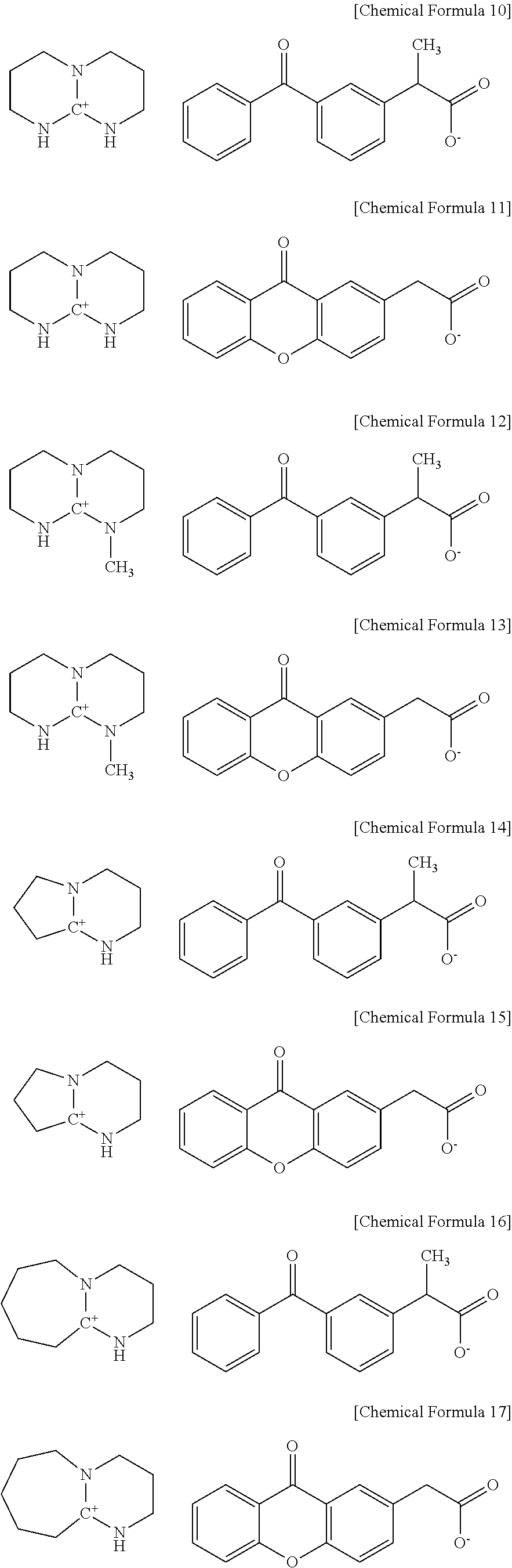

The composition may include the base generating agent in an amount of about 5 parts by weight to about 40 parts by weight, for example 7 parts by weight to about 30 parts by weight, based on about 100 parts by weight of a heat resistance polymer. In some embodiments, the composition may include the base generating agent in an amount of about 5, 6, 7, 8, 9, 10, 11, 12, 13, 14, 15, 16, 17, 18, 19, 20, 21, 22, 23, 24, 25, 26, 27, 28, 29, 30, 31, 32, 33, 34, 35, 36, 37, 38, 39 or 40 parts by weight. Further, according to some embodiments of the present invention, the amount of the base generating agent can be in a range from about any of the foregoing amounts to about any other of the foregoing amounts.
When the base generating agent is included in an amount within the above range, a pattern may be fast formed down to the bottom without lifting.
The composition for patterning a light blocking layer may include a solvent capable of easily dissolving each component such as a heat resistance polymer, a cross-linking agent, a black colorant, a base generating agent and the like.
The solvent may be an organic solvent. Examples of the solvent may include without limitation N-methyl-2-pyrrolidone, gamma-butyrolactone, N,N-dimethyl acetamide, dimethylsulfoxide, diethyleneglycoldimethylether, diethyleneglycoldiethylether, diethyleneglycoldibutylether, propylene glycolmonomethylether, dipropyleneglycolmonomethylether, propylene glycolmonomethyl ether acetate, methyllactate, ethyl lactate, butyllactate, methyl-1,3-butylene glycolacetate, 1,3-butylene glycol-3-monomethylether, methylpyruvate, ethylpyruvate, methyl-3-methoxypropionate, and the like, and combinations thereof.
The solvent may be appropriately selected depending on a process of forming a photosensitive resin film such as spin coating, slit die coating and the like.
The composition may include the solvent in an amount of about 150 parts by weight to about 4000 parts by weight, for example, about 200 parts by weight to about 3000 parts by weight, based on about 100 parts by weight of a heat resistance polymer. When the solvent is used in an amount within the above range, a film may have a sufficient thickness and also may have excellent solubility and/or coating properties.
The composition for patterning a light blocking layer may further include one or more other additives.
For example, the composition for patterning a light blocking layer may include one or more additives such as but not limited to malonic acid; 3-amino-1,2-propanediol; a coupling agent including a vinyl group or a (meth)acryloxy group; a leveling agent; a fluorine-based surfactant; a silicone-based surfactant; and/or a radical polymerization initiator, for example to prevent stains and/or spots during coating, to adjust leveling, and/or to prevent pattern residue due to non-development. The amount of the additives may be controlled depending on desired properties and can be readily determined by the skilled artisan.
In addition, the composition for patterning a light blocking layer may further include an epoxy compound as an additive to improve a close-contacting (adhesive) force and the like. Examples of the epoxy compound may include without limitation epoxy novolac acrylic carboxylate resins, orthocresol novolac epoxy resins, phenol novolac epoxy resins, tetramethylbiphenyl epoxy resins, bisphenol A epoxy resins, alicyclic epoxy resins, and the like, and combinations thereof.
When the epoxy compound is further included, a radical polymerization initiator such as a peroxide initiator and/or an azobis-based initiator may be further included.
The composition may include the epoxy compound in an amount of about 0.01 parts by weight to about 5 parts by weight based on about 100 parts by weight of the composition for patterning a light blocking layer. When the epoxy compound is used in an amount within the above range, storage capability, economically close-contacting force and other characteristics may be improved.
The composition for patterning a light blocking layer may further include a thermal latent acid generator. Examples of the thermal latent acid generator may include without limitation aryl sulfonic acids such as p-toluenesulfonic acid and/or benzene sulfonic acid; perfluoroalkyl sulfonic acids such as trifluoromethane sulfonic acid and/or trifluorobutane sulfonic acid; alkyl sulfonic acids such as methane sulfonic acid, ethane sulfonic acid, and/or butane sulfonic acid; and the like, and combinations thereof.
Another embodiment includes a method of patterning a light blocking layer. FIG. 1 is a flowchart showing an exemplary method of patterning a light blocking layer according to one embodiment of the present invention. As shown in FIG. 1 , the method can include: coating a composition including a heat resistance polymer, a cross-linking agent, a black colorant, and a solvent on a substrate to form a composition layer; coating a photoresist on the composition layer followed by heating the same to form a photoresist layer; exposing and developing the resultant photoresist layer; etching the composition layer after the development; stripping the resultant composition layer with a stripper after the etching process; and heating the resultant composition layer after the stripping process.
Unlike the conventional method of patterning a light blocking layer, a method of patterning a light blocking layer according to the embodiment may realize a fine pattern through etching and stripping processes after the exposing and developing processes.
In the heating process after the stripping process, the heating may be performed at a temperature of about 200° C. to about 600° C., for example about 220° C. to about 450° C. Conventionally, a post-baking process may be performed at a temperature ranging from about 120° C. to about 240° C. after forming the light blocking layer, but according to the embodiment, a post-baking process may maintain the temperature in a range of about 250° C. to about 600° C., for example, about 300° C. to about 450° C. and thus may reduce out-gas and/or improve heat resistance at a high temperature during a TFT process after forming the light blocking layer.
In the heating process after coating the photoresist on the composition, the heating may be performed at a temperature of about 70° C. to about 160° C., for example, about 80° C. to about 150° C.
Examples of the photoresist may include without limitation novolac-based and/or naphthoquinone diazide-based photoresists. For example, the photoresist may be a chemically amplified resist.
The etching may be wet etching. Herein, an etching solution used during the etching may be acidic.
Examples of the stripper may include without limitation propylene glycolmonomethylether (PGME), propylene glycolmonomethyletheracetate (PGMEA), ethyllactate (EL), γ-butyrolactone (GBL), tetramethylammoniumhydroxide (TMAH), potassium hydroxide (KOH), dimethylsulfoxide (DMSO), butyldiglycol (BDG), monoethanolamine (MEA), N-methylpyrrolidone (NMP), hydroxydecanoic acid (HDA), catechol, and the like, and combinations thereof.
Before the etching process after the development, the method may further include a bleaching process. Or before the stripping processes after the etching process, the method may further include a bleaching process. Herein, the bleaching process may promote dissolution of the photoresist and/or cause a reaction of a photosensitive material in a lower film.
The heat resistance polymer may be a polybenzoxazole precursor, a polyimide precursor, a novolac resin, a bisphenol A resin, a bisphenol F resin, an acrylate resin, siloxane-based resin or a combination thereof. The heat resistance polymer is the same as described above.
The cross-linking agent may include at least one of the functional group represented by Chemical Formula 1. The cross-linking agent is the same as described above.
The composition may further include a base generating agent. The base generating agent is the same as described above.
The black colorant is the same as described above. The black colorant may be carbon black, aniline black, perylene black, RGB black, cobalt oxide, titanium oxide or a combination thereof.
The composition may include about 5 parts by weight to about 40 parts by weight of the cross-linking agent, about 10 parts by weight to about 200 parts by weight of the black colorant, and about 150 parts by weight to about 4000 parts by weight of the solvent, each based on about 100 parts by weight of the heat resistance polymer.
The composition may further include one or more additives, such as but not limited to malonic acid, 3-amino-1,2-propanediol, a leveling agent, a fluorine-based surfactant, a silicone-based surfactant, a radical polymerization initiator or a combination thereof.
Hereinafter, the present invention is illustrated in more detail with reference to examples. These examples, however, are not in any sense to be interpreted as limiting the scope of the invention.
12.4 g of 2,2-bis(3-amino-4-hydroxy phenyl)-1,1,1,3,3,3-hexafluoropropane are dissolved in 125 g of N-methyl-2-pyrrolidone (NMP) in a four-necked flask equipped with an agitator, a temperature controller, a nitrogen gas injector and a cooler, while nitrogen is passed therethrough.
When the solids are completely dissolved, 4.2 g of pyridine as a catalyst is added thereto, and a solution obtained by dissolving 9.4 g of 4,4′-oxydibenzoylchloride in 100 g of NMP while its temperature is maintained at 0° C. to 5° C. is added into the four-necked flask in a dropwise fashion for 30 minutes. When the addition is complete, the mixture is reacted at 0° C. to 5° C. for one hour and then at room temperature (15° C. to 25° C.) by increasing the temperature for one hour.
Then, 1.1 g of 5-norbornene-2,3-dicarboxyl anhydride is added thereto, and the resulting mixture is agitated at 70° C. for 24 hours, completing the reaction. The reaction mixture is added to a mixed solution of water/methanol=10/1 (a volume ratio) to generate a precipitate, and the precipitate is filtered, cleaned with water, and then dried at 80° C. under vacuum for greater than or equal to 24 hours, obtaining a polybenzoxazole precursor.
10 g of the polybenzoxazole precursor is added to a mixture of 10 g of γ-butyrolactone (GBL), 140 g of propyleneglycolmonomethylether (PGME), 40 g of ethyllactate (EL) and dissolved therein, 8 g of carbon black and 2.5 g of a cross-linking agent represented by Chemical Formula B are added thereto and dissolved therein, and the solution is filtered through a 0.45 μm fluorine resin filter, obtaining a composition for patterning a light blocking layer.

A composition for patterning a light blocking layer is prepared according to the same method as Example 1 except for using 2.5 g of a base generating agent represented by Chemical Formula 10 along with the carbon black and the cross-linking agent in Example 1.

A composition for patterning a light blocking layer is prepared according to the same method as Example 1 except for using 2.5 g of a base generating agent represented by Chemical Formula 21 along with the carbon black and the cross-linking agent in Example 1.

A composition for patterning a light blocking layer is prepared according to the same method as Example 1 except for using no cross-linking agent in Example 1.
(Evaluation)
Evaluation 1: Chemical Resistance
Each composition for patterning a light blocking layer according to Examples 1 to 3 and Comparative Example 1 is coated on an 8-inch wafer by using a K-Spinner made by SEMES Co. as a spin-coater and heated on a 140° C. hot plate for 3 minutes to form a 1.5 μm-thick light blocking layer. The thickness change of the light blocking layer is examined by dipping the light blocking layer in PGMEA for 1 minute, and the results are provided in the following Table 1.
Reference for Chemical Resistance Evaluation
No thickness change: ◯
Thickness change: X
| TABLE 1 | ||
| Chemical resistance | ||
| Example 1 | ◯ | ||
| Example 2 | ◯ | ||
| Example 3 | ◯ | ||
| Comparative Example 1 | X | ||
As shown in Table 1, the compositions for patterning a light blocking layer according to Examples 1 to 3 have excellent chemical resistance compared with the composition for patterning a light blocking layer according to Comparative Example 1 and thus provides a light blocking layer capable of realizing a fine pattern.
(Evaluation)
Evaluation 2: Pattern Formation and Tapered Angle in Light-Blocking Layer
Each composition for patterning a light blocking layer according to Examples 1 to 3 and Comparative Example 1 is coated on an 8 inch wafer by using K-Spinner made by SEMES Co. as a spin-coater and then heated on a 140° C. hot plate for 3 minutes to form a 1.5 μm-thick light blocking layer. Next, the light blocking layer is coated with an i-line PR (HKT-501), the light blocking layer is heated on a 100° C. hot plate for 1 minute, forming a 1.0 μm-thick PR layer. Then, a 5 μm fine pattern is realized by splitting energy with i10C made by Nikon Co. The patterned wafer is exposed and dipped by Al etchant at 30° C. for 300 seconds (with bleaching; 1000 mL/cm2). Accordingly, the final patterned a light blocking layer is made by processing TMAH puddle process for 200 seconds. The patterned (glass) substrate is cured at 350° C. for 1 hour, its tapered angle is measured by using S-4300 made by Hitachi, Ltd., and the results are provided in Table 2.
| TABLE 2 | |||
| Formation of pattern | Tapered angle (°) | ||
| Example 1 | ◯ | 65 |
| Example 2 | ◯ | 64 |
| Example 3 | ◯ | 65 |
| Comparative Example 1 | X | — |
As shown in the Table 2, the compositions for patterning a light blocking layer according to Examples 1 to 3 form a pattern having an appropriate tapered angle compared with the composition for patterning a light blocking layer according to Comparative Example 1.
While this invention has been described in connection with what is presently considered to be practical exemplary embodiments, it is to be understood that the invention is not limited to the disclosed embodiments, but, on the contrary, is intended to cover various modifications and equivalent arrangements included within the spirit and scope of the appended claims. Therefore, the aforementioned embodiments should be understood to be exemplary but not limiting the present invention in any way.
100, 200: device
110, 180, 210, 280: substrate
120, 220: light blocking layer
130, 150, 230, 250: passivation film
140, 240: thin film transistor
160, 260: color filter
170, 270: insulation layer
Claims (16)
1. A device comprising
a substrate;
a light blocking layer on the substrate;
a passivation film covering the light blocking layer on the substrate;
a thin film transistor on the passivation film;
another passivation film covering the thin film transistor;
a color filter on said another passivation film; and
an insulation layer on said another passivation film and covering the color filter,
wherein the light blocking layer is patterned using a composition including a heat resistance polymer, a cross-linking agent, a black colorant, and a solvent,
wherein the cross-linking agent comprises at least one functional group represented by Chemical Formula 1:
and
wherein the cross-linking agent further comprises at least one or more functional groups represented by Chemical Formulae 2 to 4:

wherein, in Chemical Formulae 3 and 4,
R2 and R3 are the same or different and are each independently a hydrogen atom or a substituted or unsubstituted C1 to C10 alkyl group.
2. The device of claim 1 , wherein the heat resistance polymer is a polybenzoxazole precursor, a polyimide precursor, a novolac resin, a bisphenol A resin, a bisphenol F resin, an acrylate resin, siloxane-based resin or a combination thereof.
3. The device of claim 1 , wherein the composition further comprises a base generating agent.
4. The device of claim 3 , wherein the base generating agent is represented by Chemical Formula 5:

wherein, in Chemical Formula 5,
X is —CH2—or —NH—,
W is —O— or —S—,
n is an integer of 0 or 1,
R1 is a hydrogen atom or a substituted or unsubstituted C1 to C10 alkyl group, and
L1 is a single bond or a substituted or unsubstituted C1 to C10 alkylene group.
5. The device of claim 3 , wherein the base generating agent is represented by one or more of Chemical Formulae 6 to 9:

wherein, in Chemical Formulae 6 and 9,
X is —CH2— or —NH—,
R1 is a hydrogen atom or a substituted or unsubstituted C1 to C10 alkyl group, and
L1 is a single bond or a substituted or unsubstituted C1 to C10 alkylene group.
6. The device of claim 3 , wherein the base generating agent comprises one or more base generating agents represented by Chemical Formula 10 to Chemical Formula 21:


7. The device of claim 3 , wherein the base generating agent is included in an amount of about 5 parts by weight to about 40 parts by weight based on about 100 parts by weight of the heat resistance polymer.
8. The device of claim 1 , wherein the black colorant is carbon black, aniline black, perylene black, RGB black, cobalt oxide, titanium oxide or a combination thereof.
9. The device of claim 1 , wherein the composition comprises:
about 5 parts by weight to about 40 parts by weight of the cross-linking agent,
about 10 parts by weight to about 200 parts by weight of the black colorant,
about 150 parts by weight to about 4000 parts by weight of the solvent,
each based on about 100 parts by weight of the heat resistance polymer.
10. The device of claim 1 , wherein the composition further comprises malonic acid, 3-amino-1,2-propanediol, a leveling agent, a fluorine-based surfactant, a silicone-based surfactant, a radical polymerization initiator ora combination thereof.
11. A method of patterning a light blocking layer comprising:
coating a composition including a heat resistance polymer, a cross-linking agent, a black colorant, and a solvent on a substrate to form a composition layer;
coating a photoresist on the composition layer followed by heating the same to form a photoresist layer;
exposing and developing the resultant photoresist layer;
etching the composition layer after the development;
stripping the resultant composition layer with a stripper after the etching process; and
heating the resultant composition layer after the stripping process,
wherein the stripper comprises propylene glycol monomethyl ether (PGME), propylene glycol monomethyl ether acetate (PGMEA), ethyl lactate (EL), γ-butyrolactone (GBL), tetramethyl ammonium hydroxide (TMAH), potassium hydroxide (KOH), dimethylsulfoxide (DMSO), butyldiglycol (BDG), monoethanolamine (MEA), N-methylpyrrolidone (NMP), hydroxydecanoic acid (HDA), catechol, or a combination thereof.
12. The method of claim 11 , wherein in the heating process after the stripping process, the heating is performed at a temperature of about 200 ° C. to about 600 ° C.
13. The method of claim 11 , wherein in the heating process after coating the photoresist on the composition layer, the heating is performed at a temperature of about 70 ° C. to about 160 ° C.
14. The method of claim 11 , wherein before the etching process after the development or before the stripping process after the etching process, the method further comprises a bleaching process.
15. The method of claim 11 , wherein the cross-linking agent comprises at least one functional group represented by Chemical Formula 1:
16. The method of claim 11 , wherein the composition further comprises a base generating agent.
Applications Claiming Priority (4)
| Application Number | Priority Date | Filing Date | Title |
|---|---|---|---|
| KR20150031650 | 2015-03-06 | ||
| KR10-2015-0031650 | 2015-03-06 | ||
| KR10-2015-0128444 | 2015-09-10 | ||
| KR1020150128444A KR101916782B1 (en) | 2015-03-06 | 2015-09-10 | Device including black matrix and patterning method of the black matrix |
Publications (2)
| Publication Number | Publication Date |
|---|---|
| US20160259095A1 US20160259095A1 (en) | 2016-09-08 |
| US9709710B2 true US9709710B2 (en) | 2017-07-18 |
Family
ID=56850590
Family Applications (1)
| Application Number | Title | Priority Date | Filing Date |
|---|---|---|---|
| US14/940,337 Active US9709710B2 (en) | 2015-03-06 | 2015-11-13 | Device including light blocking layer and method of patterning the light blocking layer |
Country Status (2)
| Country | Link |
|---|---|
| US (1) | US9709710B2 (en) |
| JP (1) | JP6917675B2 (en) |
Cited By (1)
| Publication number | Priority date | Publication date | Assignee | Title |
|---|---|---|---|---|
| US20220299880A1 (en) * | 2020-09-29 | 2022-09-22 | Taiwan Semiconductor Manufacturing Company, Ltd. | Method for removing resistor layer, and method of manufacturing semiconductor |
Families Citing this family (3)
| Publication number | Priority date | Publication date | Assignee | Title |
|---|---|---|---|---|
| CN106981478A (en) * | 2017-04-07 | 2017-07-25 | 京东方科技集团股份有限公司 | Top gate type thin film transistor and preparation method thereof, array base palte, display panel |
| US10770496B2 (en) * | 2018-04-16 | 2020-09-08 | Visera Technologies Company Limited | Optical sensors and methods for forming the same |
| CN111176070B (en) * | 2018-11-12 | 2023-09-01 | 台湾永光化学工业股份有限公司 | Negative photoresist composition and use thereof |
Citations (19)
| Publication number | Priority date | Publication date | Assignee | Title |
|---|---|---|---|---|
| JPH0784122A (en) | 1993-07-23 | 1995-03-31 | Toray Ind Inc | Production of color filter |
| US6583830B2 (en) * | 2000-04-21 | 2003-06-24 | Seiko Epson Corporation | Electrooptical device, projection-type display apparatus, and method for manufacturing the electrooptical device |
| US20060020068A1 (en) | 2004-07-07 | 2006-01-26 | Edmund Elce | Photosensitive compositions based on polycyclic polymers for low stress, high temperature films |
| JP2006350029A (en) | 2005-06-16 | 2006-12-28 | Sekisui Chem Co Ltd | Black resist composition |
| US7476476B2 (en) | 2003-06-02 | 2009-01-13 | Toray Industries, Inc. | Photosensitive resin composition, electronic component using the same, and display unit using the same |
| US20090202822A1 (en) * | 2006-05-26 | 2009-08-13 | Nitto Denko Corporation | Polarizer protective film, polarizing plate, and image display apparatus |
| JP2009222792A (en) | 2008-03-13 | 2009-10-01 | Fujifilm Corp | Photosensitive resin composition, and method for forming light-shielding image |
| US20100060830A1 (en) * | 2008-09-08 | 2010-03-11 | Nitto Denko Corporation | Method of manufacturing light diffusion film, light diffusion film, polarizing plate, and liquid crystal display |
| US20110147757A1 (en) * | 2009-12-17 | 2011-06-23 | Samsung Mobile Display Co., Ltd. | Array substrate of display device |
| US20110278720A1 (en) * | 2009-02-04 | 2011-11-17 | Panasonic Corporation | Semiconductor substrate structure and semiconductor device |
| JP4821680B2 (en) | 2007-03-30 | 2011-11-24 | 大日本印刷株式会社 | Base proliferating agent, resin composition using the same, and article |
| US20120033151A1 (en) * | 2010-08-06 | 2012-02-09 | Semiconductor Energy Laboratory Co., Ltd. | Liquid crystal display device and driving method thereof |
| US20120183751A1 (en) | 2009-09-30 | 2012-07-19 | Dai Nippon Printing Co., Ltd. | Base generator, photosensitive resin composition, pattern forming material comprising the photosensitive resin composition, pattern forming method using the photosensitive resin composition and products comprising the same |
| US20120285929A1 (en) * | 2011-05-11 | 2012-11-15 | Jsr Corporation | Pattern-forming method, and composition for forming resist underlayer film |
| US20120318854A1 (en) | 2011-06-15 | 2012-12-20 | Promerus Llc | Thermally decomposable polymer compositions incorporating thermally activated base generators |
| US20130280655A1 (en) * | 2010-12-28 | 2013-10-24 | Mitsubishi Gas Chemical Company, Inc. | Aromatic hydrocarbon resin, underlayer film forming composition for lithography, and method for forming multilayer resist pattern |
| KR20140043443A (en) | 2011-06-24 | 2014-04-09 | 도오꾜오까고오교 가부시끼가이샤 | Negative-type photosensitive resin composition, pattern forming method, cured film, insulating film, color filter, and display device |
| KR20140075872A (en) | 2012-12-10 | 2014-06-20 | 엘지디스플레이 주식회사 | Photosensitive Composition for Display Device, Black Matrix Having the Composition, and Process for forming Patterns of Black Matrix Using the Composition |
| JP2015007766A (en) | 2013-05-27 | 2015-01-15 | 富士フイルム株式会社 | Method for producing color filter, composition for forming base layer, and organic el display device |
Family Cites Families (16)
| Publication number | Priority date | Publication date | Assignee | Title |
|---|---|---|---|---|
| JPH06230215A (en) * | 1993-02-05 | 1994-08-19 | Sumitomo Chem Co Ltd | Positive type resist composition for black matrix |
| JPH08286026A (en) * | 1995-04-19 | 1996-11-01 | Toppan Printing Co Ltd | Black matrix substrate and color filter using the same |
| JPH08334893A (en) * | 1995-06-09 | 1996-12-17 | Japan Synthetic Rubber Co Ltd | Radiation sensitive composition |
| JP3420000B2 (en) * | 1996-09-06 | 2003-06-23 | 株式会社東芝 | Black colored composition, high heat-resistant light-blocking member, array substrate, liquid crystal display device, and method of manufacturing array substrate |
| JP2001175198A (en) * | 1999-12-14 | 2001-06-29 | Semiconductor Energy Lab Co Ltd | Semiconductor device and manufacturing method therefor |
| JP2002244294A (en) * | 2001-02-20 | 2002-08-30 | Nippon Zeon Co Ltd | Resist composition and resist pattern forming method |
| JP2005266189A (en) * | 2004-03-18 | 2005-09-29 | Sumitomo Bakelite Co Ltd | Photosensitive resin composition, and semiconductor device and display element using the same |
| JP4499471B2 (en) * | 2004-04-28 | 2010-07-07 | 関西ペイント株式会社 | Photosensitive resin composition |
| JP2009003442A (en) * | 2007-05-23 | 2009-01-08 | Mitsubishi Chemicals Corp | Photosensitive resin composition, liquid crystal alignment control rib, spacer, color filter and image display device |
| JP2010097214A (en) * | 2008-09-19 | 2010-04-30 | Toray Ind Inc | Color filter substrate for liquid crystal display apparatus and liquid crystal display apparatus |
| JP2010080687A (en) * | 2008-09-26 | 2010-04-08 | Fujifilm Corp | Lightproof film forming method, and solid state imaging element manufacturing method |
| JP6011956B2 (en) * | 2010-04-14 | 2016-10-25 | 学校法人東京理科大学 | Photosensitive resin composition |
| JP5940259B2 (en) * | 2010-08-06 | 2016-06-29 | 三洋化成工業株式会社 | Photosensitive composition |
| JP5803635B2 (en) * | 2011-12-07 | 2015-11-04 | Jsr株式会社 | Positive radiation-sensitive composition, cured film, and method for forming cured film |
| KR20140087693A (en) * | 2012-12-31 | 2014-07-09 | 삼성디스플레이 주식회사 | Thin film transistor, thin film transistor array panel including the same and manufacturing method thereof |
| JP2014164070A (en) * | 2013-02-25 | 2014-09-08 | Seiko Epson Corp | Color filter substrate, electro-optic device, method for manufacturing electro-optic device and electronic equipment |
-
2015
- 2015-11-13 US US14/940,337 patent/US9709710B2/en active Active
- 2015-11-20 JP JP2015227953A patent/JP6917675B2/en active Active
Patent Citations (24)
| Publication number | Priority date | Publication date | Assignee | Title |
|---|---|---|---|---|
| JPH0784122A (en) | 1993-07-23 | 1995-03-31 | Toray Ind Inc | Production of color filter |
| US6583830B2 (en) * | 2000-04-21 | 2003-06-24 | Seiko Epson Corporation | Electrooptical device, projection-type display apparatus, and method for manufacturing the electrooptical device |
| JP4371110B2 (en) | 2003-06-02 | 2009-11-25 | 東レ株式会社 | Photosensitive resin composition, electronic component using the same, and display device |
| US7476476B2 (en) | 2003-06-02 | 2009-01-13 | Toray Industries, Inc. | Photosensitive resin composition, electronic component using the same, and display unit using the same |
| US20060020068A1 (en) | 2004-07-07 | 2006-01-26 | Edmund Elce | Photosensitive compositions based on polycyclic polymers for low stress, high temperature films |
| KR20090040483A (en) | 2004-07-07 | 2009-04-24 | 프로메러스, 엘엘씨 | Photosensitive compositions based on polycyclic polymers |
| JP2006350029A (en) | 2005-06-16 | 2006-12-28 | Sekisui Chem Co Ltd | Black resist composition |
| US20090202822A1 (en) * | 2006-05-26 | 2009-08-13 | Nitto Denko Corporation | Polarizer protective film, polarizing plate, and image display apparatus |
| JP4821680B2 (en) | 2007-03-30 | 2011-11-24 | 大日本印刷株式会社 | Base proliferating agent, resin composition using the same, and article |
| JP2009222792A (en) | 2008-03-13 | 2009-10-01 | Fujifilm Corp | Photosensitive resin composition, and method for forming light-shielding image |
| US20100060830A1 (en) * | 2008-09-08 | 2010-03-11 | Nitto Denko Corporation | Method of manufacturing light diffusion film, light diffusion film, polarizing plate, and liquid crystal display |
| US20110278720A1 (en) * | 2009-02-04 | 2011-11-17 | Panasonic Corporation | Semiconductor substrate structure and semiconductor device |
| KR20120090050A (en) | 2009-09-30 | 2012-08-16 | 다이니폰 인사츠 가부시키가이샤 | Base-generating agent, photosensitive resin composition, material for pattern-forming comprising said photosensitive resin composition, pattern-forming method using said photosensitive resin composition, and article |
| US20120183751A1 (en) | 2009-09-30 | 2012-07-19 | Dai Nippon Printing Co., Ltd. | Base generator, photosensitive resin composition, pattern forming material comprising the photosensitive resin composition, pattern forming method using the photosensitive resin composition and products comprising the same |
| US20110147757A1 (en) * | 2009-12-17 | 2011-06-23 | Samsung Mobile Display Co., Ltd. | Array substrate of display device |
| US20120033151A1 (en) * | 2010-08-06 | 2012-02-09 | Semiconductor Energy Laboratory Co., Ltd. | Liquid crystal display device and driving method thereof |
| US20130280655A1 (en) * | 2010-12-28 | 2013-10-24 | Mitsubishi Gas Chemical Company, Inc. | Aromatic hydrocarbon resin, underlayer film forming composition for lithography, and method for forming multilayer resist pattern |
| US20120285929A1 (en) * | 2011-05-11 | 2012-11-15 | Jsr Corporation | Pattern-forming method, and composition for forming resist underlayer film |
| US20120318854A1 (en) | 2011-06-15 | 2012-12-20 | Promerus Llc | Thermally decomposable polymer compositions incorporating thermally activated base generators |
| JP2014525835A (en) | 2011-06-15 | 2014-10-02 | プロメラス, エルエルシー | Thermally decomposable polymer composition comprising a heat activated base generator |
| KR20140043443A (en) | 2011-06-24 | 2014-04-09 | 도오꾜오까고오교 가부시끼가이샤 | Negative-type photosensitive resin composition, pattern forming method, cured film, insulating film, color filter, and display device |
| US20140231729A1 (en) | 2011-06-24 | 2014-08-21 | Tokyo Ohka Kogyo Co., Ltd. | Negative-type photosensitive resin composition, pattern forming method, cured film, insulating film, color filter, and display device |
| KR20140075872A (en) | 2012-12-10 | 2014-06-20 | 엘지디스플레이 주식회사 | Photosensitive Composition for Display Device, Black Matrix Having the Composition, and Process for forming Patterns of Black Matrix Using the Composition |
| JP2015007766A (en) | 2013-05-27 | 2015-01-15 | 富士フイルム株式会社 | Method for producing color filter, composition for forming base layer, and organic el display device |
Non-Patent Citations (1)
| Title |
|---|
| Search Report in counterpart Taiwanese Application No. 104136566 dated Apr. 6, 2016, pp. 1. |
Cited By (2)
| Publication number | Priority date | Publication date | Assignee | Title |
|---|---|---|---|---|
| US20220299880A1 (en) * | 2020-09-29 | 2022-09-22 | Taiwan Semiconductor Manufacturing Company, Ltd. | Method for removing resistor layer, and method of manufacturing semiconductor |
| US11789366B2 (en) * | 2020-09-29 | 2023-10-17 | Taiwan Semiconductor Manufacturing Company, Ltd. | Method for removing resist layer, and method of manufacturing semiconductor |
Also Published As
| Publication number | Publication date |
|---|---|
| JP6917675B2 (en) | 2021-08-11 |
| US20160259095A1 (en) | 2016-09-08 |
| JP2016164646A (en) | 2016-09-08 |
Similar Documents
| Publication | Publication Date | Title |
|---|---|---|
| US8815489B2 (en) | Positive photosensitive resin composition, photosensitive resin film prepared by using the same, and semiconductor device including the photosensitive resin film | |
| TWI548945B (en) | Positive photosensitive resin composition, photosensitive resin film and display device using the same | |
| US9709710B2 (en) | Device including light blocking layer and method of patterning the light blocking layer | |
| US9482943B2 (en) | Positive photosensitive resin composition, and photosensitive resin film and display device prepared by using the same | |
| US9429842B2 (en) | Positive photosensitive resin composition, photosensitive resin film prepared by using the same, and display device | |
| KR101812580B1 (en) | Positive photosensitive resin composition, photosensitive resin film, and display device using the same | |
| US8987342B2 (en) | Photosensitive resin composition for insulating film of display device, insulating film using the same, and display device using the same | |
| US9040213B2 (en) | Positive photosensitive resin composition, photosensitive resin film prepared by using the same, and semiconductor device including the photosensitive resin film | |
| US9329475B2 (en) | Positive photosensitive resin composition, photosensitive resin film prepared by using the same, and display device | |
| KR101916782B1 (en) | Device including black matrix and patterning method of the black matrix | |
| KR20160104380A (en) | Positive photosensitive resin composition, photosensitive resin film and display device using the same | |
| KR102044944B1 (en) | Photosensitive resin composition, photosensitive resin layer using the same and display device | |
| KR101423172B1 (en) | Positive photosensitive resin composition, photosensitive resin film prepared by using the same, and semiconductor device including the photosensitive resin film | |
| TWI738071B (en) | Photosensitive resin composition, photosensitive resin layer and electronic device | |
| TW201425417A (en) | Photosensitive resin composition for insulating film of display device, insulating film using the same, and display device using the same | |
| JP2015114355A (en) | Positive photosensitive resin composition | |
| KR102149967B1 (en) | Photosensitive resin composition and photosensitive resin layer using the same | |
| TWI709820B (en) | Positive photosensitive resin composition, photosensitive resin layer and electronic device | |
| TWI696038B (en) | Photosensitive resin composition, photosensitive resin layer using the same and electronic device | |
| KR101720717B1 (en) | Positive photosensitive resin composition, photosensitive resin film, and display device using the same | |
| KR102319968B1 (en) | Positive photosensitive resin composition, photosensitive resin layer and electronic device using the same | |
| KR101881943B1 (en) | Positive photosensitive resin composition, photosensitive resin film and display device using the same |
Legal Events
| Date | Code | Title | Description |
|---|---|---|---|
| AS | Assignment |
Owner name: SAMSUNG SDI CO., LTD., KOREA, REPUBLIC OF Free format text: ASSIGNMENT OF ASSIGNORS INTEREST;ASSIGNORS:KIM, SANG-SOO;KANG, JIN-HEE;KIM, CHAN-WOO;AND OTHERS;REEL/FRAME:037031/0587 Effective date: 20150930 |
|
| STCF | Information on status: patent grant |
Free format text: PATENTED CASE |
|
| CC | Certificate of correction | ||
| MAFP | Maintenance fee payment |
Free format text: PAYMENT OF MAINTENANCE FEE, 4TH YEAR, LARGE ENTITY (ORIGINAL EVENT CODE: M1551); ENTITY STATUS OF PATENT OWNER: LARGE ENTITY Year of fee payment: 4 |