US9691670B2 - Manufacturing method of array substrate - Google Patents
Manufacturing method of array substrate Download PDFInfo
- Publication number
- US9691670B2 US9691670B2 US14/127,264 US201214127264A US9691670B2 US 9691670 B2 US9691670 B2 US 9691670B2 US 201214127264 A US201214127264 A US 201214127264A US 9691670 B2 US9691670 B2 US 9691670B2
- Authority
- US
- United States
- Prior art keywords
- gate
- short circuit
- open circuit
- common electrode
- manufacturing
- Prior art date
- Legal status (The legal status is an assumption and is not a legal conclusion. Google has not performed a legal analysis and makes no representation as to the accuracy of the status listed.)
- Expired - Fee Related, expires
Links
- 238000004519 manufacturing process Methods 0.000 title claims abstract description 24
- 239000000758 substrate Substances 0.000 title claims abstract description 23
- 238000001514 detection method Methods 0.000 claims abstract description 24
- 238000002161 passivation Methods 0.000 claims description 11
- 239000000463 material Substances 0.000 claims description 6
- 238000005530 etching Methods 0.000 claims description 4
- 230000007547 defect Effects 0.000 description 13
- 238000000034 method Methods 0.000 description 9
- 239000004973 liquid crystal related substance Substances 0.000 description 5
- 230000002159 abnormal effect Effects 0.000 description 2
- 238000010586 diagram Methods 0.000 description 2
- 238000012986 modification Methods 0.000 description 2
- 230000004048 modification Effects 0.000 description 2
- XUIMIQQOPSSXEZ-UHFFFAOYSA-N Silicon Chemical compound [Si] XUIMIQQOPSSXEZ-UHFFFAOYSA-N 0.000 description 1
- 230000002950 deficient Effects 0.000 description 1
- 238000000151 deposition Methods 0.000 description 1
- 230000010354 integration Effects 0.000 description 1
- 230000008054 signal transmission Effects 0.000 description 1
- 229910052710 silicon Inorganic materials 0.000 description 1
- 239000010703 silicon Substances 0.000 description 1
- 239000010409 thin film Substances 0.000 description 1
Images


Classifications
-
- H—ELECTRICITY
- H01—ELECTRIC ELEMENTS
- H01L—SEMICONDUCTOR DEVICES NOT COVERED BY CLASS H10
- H01L22/00—Testing or measuring during manufacture or treatment; Reliability measurements, i.e. testing of parts without further processing to modify the parts as such; Structural arrangements therefor
- H01L22/10—Measuring as part of the manufacturing process
- H01L22/14—Measuring as part of the manufacturing process for electrical parameters, e.g. resistance, deep-levels, CV, diffusions by electrical means
-
- G—PHYSICS
- G02—OPTICS
- G02F—OPTICAL DEVICES OR ARRANGEMENTS FOR THE CONTROL OF LIGHT BY MODIFICATION OF THE OPTICAL PROPERTIES OF THE MEDIA OF THE ELEMENTS INVOLVED THEREIN; NON-LINEAR OPTICS; FREQUENCY-CHANGING OF LIGHT; OPTICAL LOGIC ELEMENTS; OPTICAL ANALOGUE/DIGITAL CONVERTERS
- G02F1/00—Devices or arrangements for the control of the intensity, colour, phase, polarisation or direction of light arriving from an independent light source, e.g. switching, gating or modulating; Non-linear optics
- G02F1/01—Devices or arrangements for the control of the intensity, colour, phase, polarisation or direction of light arriving from an independent light source, e.g. switching, gating or modulating; Non-linear optics for the control of the intensity, phase, polarisation or colour
- G02F1/13—Devices or arrangements for the control of the intensity, colour, phase, polarisation or direction of light arriving from an independent light source, e.g. switching, gating or modulating; Non-linear optics for the control of the intensity, phase, polarisation or colour based on liquid crystals, e.g. single liquid crystal display cells
- G02F1/133—Constructional arrangements; Operation of liquid crystal cells; Circuit arrangements
- G02F1/136—Liquid crystal cells structurally associated with a semi-conducting layer or substrate, e.g. cells forming part of an integrated circuit
- G02F1/1362—Active matrix addressed cells
-
- H—ELECTRICITY
- H01—ELECTRIC ELEMENTS
- H01L—SEMICONDUCTOR DEVICES NOT COVERED BY CLASS H10
- H01L27/00—Devices consisting of a plurality of semiconductor or other solid-state components formed in or on a common substrate
- H01L27/02—Devices consisting of a plurality of semiconductor or other solid-state components formed in or on a common substrate including semiconductor components specially adapted for rectifying, oscillating, amplifying or switching and having potential barriers; including integrated passive circuit elements having potential barriers
- H01L27/12—Devices consisting of a plurality of semiconductor or other solid-state components formed in or on a common substrate including semiconductor components specially adapted for rectifying, oscillating, amplifying or switching and having potential barriers; including integrated passive circuit elements having potential barriers the substrate being other than a semiconductor body, e.g. an insulating body
- H01L27/1214—Devices consisting of a plurality of semiconductor or other solid-state components formed in or on a common substrate including semiconductor components specially adapted for rectifying, oscillating, amplifying or switching and having potential barriers; including integrated passive circuit elements having potential barriers the substrate being other than a semiconductor body, e.g. an insulating body comprising a plurality of TFTs formed on a non-semiconducting substrate, e.g. driving circuits for AMLCDs
- H01L27/1259—Multistep manufacturing methods
- H01L27/1262—Multistep manufacturing methods with a particular formation, treatment or coating of the substrate
-
- G—PHYSICS
- G02—OPTICS
- G02F—OPTICAL DEVICES OR ARRANGEMENTS FOR THE CONTROL OF LIGHT BY MODIFICATION OF THE OPTICAL PROPERTIES OF THE MEDIA OF THE ELEMENTS INVOLVED THEREIN; NON-LINEAR OPTICS; FREQUENCY-CHANGING OF LIGHT; OPTICAL LOGIC ELEMENTS; OPTICAL ANALOGUE/DIGITAL CONVERTERS
- G02F1/00—Devices or arrangements for the control of the intensity, colour, phase, polarisation or direction of light arriving from an independent light source, e.g. switching, gating or modulating; Non-linear optics
- G02F1/01—Devices or arrangements for the control of the intensity, colour, phase, polarisation or direction of light arriving from an independent light source, e.g. switching, gating or modulating; Non-linear optics for the control of the intensity, phase, polarisation or colour
- G02F1/13—Devices or arrangements for the control of the intensity, colour, phase, polarisation or direction of light arriving from an independent light source, e.g. switching, gating or modulating; Non-linear optics for the control of the intensity, phase, polarisation or colour based on liquid crystals, e.g. single liquid crystal display cells
- G02F1/133—Constructional arrangements; Operation of liquid crystal cells; Circuit arrangements
- G02F1/136—Liquid crystal cells structurally associated with a semi-conducting layer or substrate, e.g. cells forming part of an integrated circuit
- G02F1/1362—Active matrix addressed cells
- G02F1/136254—Checking; Testing
-
- G02F2001/136254—
Definitions
- Embodiments of the present invention relate to a manufacturing method of an array substrate.
- Gate Driver on Array (GOA) technology as a substitute for the process technology in which fabricating a driving chip by an external connecting silicon wafer, is an emerging technology in a liquid crystal display field, in which a gate driving circuit is directly fabricated on an array substrate.
- the application of the GOA technology may decrease the number of producing processes and the product cost and may improve the integration level of a thin film transistor-liquid crystal display (TFT-LCD) panel.
- TFT-LCD thin film transistor-liquid crystal display
- An embodiment of the present invention provides a manufacturing method of an array substrate comprising: forming a gate detecting pattern on the array substrate with gate lines and common electrode lines formed thereon, the gate detecting pattern being arranged on one side of a pixel region of the array substrate and used to connect all the common electrode lines for pixel units; and performing a short circuit or a open circuit detection, wherein if the difference between a signal received by a receiving terminal for a gate line and a signal transmitted from a transmitting terminal for the gate line is larger than a predetermined detection threshold value, it is determined that short circuit between the gate line and a common electrode line or open circuit in the gate line occurs.
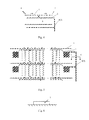
- FIG. 1 is a schematic view for showing a gate pattern of a 20 inches GOA product in a related art
- FIG. 2 is a circuit diagram of the gate pattern of the 20 inches GOA product in the related art
- FIG. 3 is a flow chart of a manufacturing method according to an embodiment of the present invention.
- FIG. 4 is a schematic view for showing a gate pattern utilized in the manufacturing method according to an embodiment of the present invention.
- FIG. 5 is a circuit diagram of the gate pattern utilized in the manufacturing method according to an embodiment of the present invention.
- FIG. 6 is a cross-sectional view taken along a line A-A′ of FIG. 5 after completion of a step S 1 in the manufacturing method according to an embodiment of the present invention
- FIG. 7 is a cross-sectional view taken along the line A-A′ of FIG. 5 after completion of steps S 2 and S 3 in the manufacturing method according to an embodiment of the present invention
- FIG. 8 is a cross-sectional view taken along the line A-A′ of FIG. 5 after completion of a step S 4 in the manufacturing method according to an embodiment of the present invention.
- a design for a gate pattern of a GOA product with a size of 20 inches is that: the gate line and common electrode line both are suspended at both sides of a pixel region; according to a detecting principle of a current open circuit/short circuit detector, in a case that a short circuit defect occurs between the gate line and the common electrode line (GCS), a sensor of the open circuit/short circuit detector may not be may not receive a significant influenced signal, and the short circuit defect can not be detected out (as shown in FIG. 1 and FIG. 2 ), thus disturbing detection for the short circuit defect.
- an undetected GCS defect may cause abnormal lighting of the liquid crystal panel, and degrade the panel as a NG level panel, and the yield is disadvantageously influenced.
- FIG. 1 and FIG. 2 show gate lines 1 and common electrode lines 2 in two adjacent pixel units, wherein the reference number 6 denotes a short circuit line, illustrating short circuit occurs between the gate line 1 and the common electrode line 2 .
- One of the objects of embodiments of the present invention is to improve the ability for detecting short circuit between a gate line and a common electrode line during manufacturing an array substrate.
- the manufacturing method comprises the following steps.
- the gate detecting pattern 8 is a detecting line 3 arranged on one side of a pixel region.
- the detecting line 3 is not electrically or physically connected to any one of the plurality of gate lines 1 .
- the detecting line 3 electrically and physically connects all the common electrode lines 2 for pixel units, as shown in FIG. 4 and FIG. 5 .
- FIG. 5 show the gate lines 1 and the common electrode lines 2 in two adjacent pixel units, wherein the reference number 6 denotes a short circuit line, illustrating that short circuit occurs between the gate line 1 and the common electrode line 2 located on an upper portion of FIG. 4 .
- FIG. 6 shows a cross-sectional view taken along a line A-A′ of FIG. 5 after completion of the step S 1 .
- the signal received by the receiving terminal 5 for the gate line 1 is detected to be far smaller than the signal transmitted from the transmitting terminal 4 , that is, the difference of the signal received by the receiving terminal 5 for the gate line 1 and the signal transmitted from the transmitting terminal 4 is above a predetermined detection threshold value, then it is determined that a defect occurs at a certain position of the gate line (short circuit between the gate line and the common electrode line or open circuit of the gate line). Then, a position detection sensor of the open circuit/short circuit detector is utilized to find out a position information of the generated defect along the gate line 1 and upload it to a server, so that a following repairing process can perform a judging operation (to determine the type of the defect) and a repairing operation.
- the detection of the defect can avoid a consequent influence on the quality of the array substrate and even the liquid crystal panel, and because the ability for detecting a GCS defect by the detector is improved, the number of missed defects is reduced. Also, defective products can be corrected by repairing gate layer, thus avoiding being discarded due to CGS defect.
- a making procedure of the patterned passivation layer 7 comprises, for example, depositing a passivation layer on the array substrate with the detecting line 3 formed thereon; and etching away the passivation layer around the detecting line 3 to uncover the detecting line 3 , as shown in FIG. 7 .
- a common electrode layer 9 (whose material can be transparent conductive oxide material, such as, ITO) can be formed on the patterned passivation layer 7 , as shown in FIG. 8 .
- all the common electrode lines for the pixel units are connected together by the detecting line on one side of the pixel region so as to facilitate the detection of short circuit or the open circuit defect by the open circuit/short circuit detector during testing the array substrate. Therefore, during manufacturing the array substrate, the ability for detecting the short circuit between the gate line and the common electrode line or for the open circuit of the gate line is improved, and abnormal lighting of the liquid crystal panel due to the GCS defect can be avoided; Also, since the detecting line which is only used for detecting the short circuit or the open circuit is etched away in a following process, signal transmission of a resultant array substrate will not be influenced.
- a manufacturing method of an array substrate comprising:
- a gate detecting pattern on the array substrate with gate lines and common electrode lines formed thereon, the gate detecting pattern being arranged on one side of a pixel region of the array substrate and used to connect all the common electrode lines for pixel units;
Landscapes
- Engineering & Computer Science (AREA)
- Physics & Mathematics (AREA)
- Microelectronics & Electronic Packaging (AREA)
- Nonlinear Science (AREA)
- Manufacturing & Machinery (AREA)
- Power Engineering (AREA)
- General Physics & Mathematics (AREA)
- Computer Hardware Design (AREA)
- Chemical & Material Sciences (AREA)
- Optics & Photonics (AREA)
- Crystallography & Structural Chemistry (AREA)
- Mathematical Physics (AREA)
- Condensed Matter Physics & Semiconductors (AREA)
- Liquid Crystal (AREA)
- Devices For Indicating Variable Information By Combining Individual Elements (AREA)
- Testing Of Short-Circuits, Discontinuities, Leakage, Or Incorrect Line Connections (AREA)
Abstract
Description
Claims (9)
Applications Claiming Priority (4)
| Application Number | Priority Date | Filing Date | Title |
|---|---|---|---|
| CN201210227079.2A CN102723311B (en) | 2012-06-29 | 2012-06-29 | Array substrate measuring method |
| CN201210227079 | 2012-06-29 | ||
| CN201210227079.2 | 2012-06-29 | ||
| PCT/CN2012/084412 WO2014000365A1 (en) | 2012-06-29 | 2012-11-09 | Array substrate manufacturing method |
Publications (2)
| Publication Number | Publication Date |
|---|---|
| US20150332979A1 US20150332979A1 (en) | 2015-11-19 |
| US9691670B2 true US9691670B2 (en) | 2017-06-27 |
Family
ID=46949033
Family Applications (1)
| Application Number | Title | Priority Date | Filing Date |
|---|---|---|---|
| US14/127,264 Expired - Fee Related US9691670B2 (en) | 2012-06-29 | 2012-11-09 | Manufacturing method of array substrate |
Country Status (3)
| Country | Link |
|---|---|
| US (1) | US9691670B2 (en) |
| CN (1) | CN102723311B (en) |
| WO (1) | WO2014000365A1 (en) |
Families Citing this family (11)
| Publication number | Priority date | Publication date | Assignee | Title |
|---|---|---|---|---|
| CN102723311B (en) | 2012-06-29 | 2014-11-05 | 京东方科技集团股份有限公司 | Array substrate measuring method |
| CN103487955B (en) * | 2013-09-02 | 2016-06-01 | 京东方科技集团股份有限公司 | A kind of short circuit measuring method |
| CN103499892B (en) * | 2013-09-29 | 2016-02-24 | 京东方科技集团股份有限公司 | Grid line break-make detection method and checkout equipment |
| CN104991388B (en) * | 2015-07-17 | 2018-05-29 | 京东方科技集团股份有限公司 | Display panel, touch panel, liquid crystal display device and its test method |
| KR102426757B1 (en) * | 2016-04-25 | 2022-07-29 | 삼성디스플레이 주식회사 | Display device and driving method thereof |
| CN107665863B (en) * | 2016-07-29 | 2020-02-07 | 京东方科技集团股份有限公司 | Pixel structure and manufacturing method thereof, array substrate and manufacturing method thereof, and display device |
| CN106409263B (en) * | 2016-11-29 | 2020-05-22 | 海信视像科技股份有限公司 | Liquid crystal panel and line short-circuit protection method thereof |
| CN107633810B (en) | 2017-10-27 | 2019-10-11 | 京东方科技集团股份有限公司 | Pixel circuit compensation method and device, display panel and display device |
| CN108628022B (en) * | 2018-06-26 | 2020-07-03 | 深圳市华星光电半导体显示技术有限公司 | Liquid crystal display and preparation method thereof |
| CN109188743A (en) * | 2018-11-14 | 2019-01-11 | 惠科股份有限公司 | Display panel manufacturing method and display device |
| CN113741102A (en) * | 2020-05-28 | 2021-12-03 | 合肥鑫晟光电科技有限公司 | Array substrate, display panel and preparation method |
Citations (10)
| Publication number | Priority date | Publication date | Assignee | Title |
|---|---|---|---|---|
| US20050024315A1 (en) * | 2000-04-06 | 2005-02-03 | Fujitsu Limited | Semiconductor integrated circuit for driving liquid crystal panel |
| US6999153B2 (en) | 2000-12-30 | 2006-02-14 | Boe-Hydis Technology Co., Ltd. | Liquid crystal display for testing defects of wiring in panel |
| CN1996032A (en) | 2006-01-06 | 2007-07-11 | Nec液晶技术株式会社 | Method of testing wires and apparatus for doing the same |
| US20090194883A1 (en) * | 2008-02-04 | 2009-08-06 | Wei Qin | Data line structure in lead region and manufacturing method thereof |
| CN101556382A (en) | 2008-04-10 | 2009-10-14 | 北京京东方光电科技有限公司 | TFT-LCD array substrate and methods for manufacturing and testing same |
| US20090315817A1 (en) * | 2008-06-23 | 2009-12-24 | Au Optronics Corporation | Lcd panel apparatus and testing method using the same |
| US20110092000A1 (en) * | 2008-05-22 | 2011-04-21 | Stmicroelectronics (Rousset) Sas | Method for manufacturing and testing an integrated electronic circuit |
| CN102253550A (en) | 2003-06-02 | 2011-11-23 | 乐金显示有限公司 | Method and apparatus for inspecting and repairing liquid crystal display device |
| CN102723311A (en) | 2012-06-29 | 2012-10-10 | 京东方科技集团股份有限公司 | Array substrate measuring method |
| US20120262184A1 (en) * | 2011-04-14 | 2012-10-18 | Au Optronics Corporation | Display panel and testing method thereof |
Family Cites Families (4)
| Publication number | Priority date | Publication date | Assignee | Title |
|---|---|---|---|---|
| KR100333271B1 (en) * | 1999-07-05 | 2002-04-24 | 구본준, 론 위라하디락사 | TFT-LCD array substrate for short or open testing of electric line and a method for fabricating the same |
| KR101246830B1 (en) * | 2006-06-09 | 2013-03-28 | 삼성디스플레이 주식회사 | Display device and method of driving the same |
| KR101294230B1 (en) * | 2006-11-30 | 2013-08-07 | 엘지디스플레이 주식회사 | Array substrate for Liquid crystal display device |
| CN101295717B (en) * | 2007-04-25 | 2010-07-14 | 北京京东方光电科技有限公司 | Thin-film transistor panel and its production method |
-
2012
- 2012-06-29 CN CN201210227079.2A patent/CN102723311B/en not_active Expired - Fee Related
- 2012-11-09 US US14/127,264 patent/US9691670B2/en not_active Expired - Fee Related
- 2012-11-09 WO PCT/CN2012/084412 patent/WO2014000365A1/en active Application Filing
Patent Citations (11)
| Publication number | Priority date | Publication date | Assignee | Title |
|---|---|---|---|---|
| US20050024315A1 (en) * | 2000-04-06 | 2005-02-03 | Fujitsu Limited | Semiconductor integrated circuit for driving liquid crystal panel |
| US6999153B2 (en) | 2000-12-30 | 2006-02-14 | Boe-Hydis Technology Co., Ltd. | Liquid crystal display for testing defects of wiring in panel |
| CN102253550A (en) | 2003-06-02 | 2011-11-23 | 乐金显示有限公司 | Method and apparatus for inspecting and repairing liquid crystal display device |
| CN1996032A (en) | 2006-01-06 | 2007-07-11 | Nec液晶技术株式会社 | Method of testing wires and apparatus for doing the same |
| US20070158812A1 (en) | 2006-01-06 | 2007-07-12 | Nec Lcd Technologies, Ltd. | Method of testing wires and apparatus for doing the same |
| US20090194883A1 (en) * | 2008-02-04 | 2009-08-06 | Wei Qin | Data line structure in lead region and manufacturing method thereof |
| CN101556382A (en) | 2008-04-10 | 2009-10-14 | 北京京东方光电科技有限公司 | TFT-LCD array substrate and methods for manufacturing and testing same |
| US20110092000A1 (en) * | 2008-05-22 | 2011-04-21 | Stmicroelectronics (Rousset) Sas | Method for manufacturing and testing an integrated electronic circuit |
| US20090315817A1 (en) * | 2008-06-23 | 2009-12-24 | Au Optronics Corporation | Lcd panel apparatus and testing method using the same |
| US20120262184A1 (en) * | 2011-04-14 | 2012-10-18 | Au Optronics Corporation | Display panel and testing method thereof |
| CN102723311A (en) | 2012-06-29 | 2012-10-10 | 京东方科技集团股份有限公司 | Array substrate measuring method |
Non-Patent Citations (4)
| Title |
|---|
| First Chinese Office Action Dated Sep. 27, 2013 Appln. No. 201210227079.2. |
| International Preliminary Report on Patentability Appln. No. PCT/CN2012/084412; Dated Dec. 31, 2014. |
| International Search Report Dated Mar. 27, 2013 Appln. No. PCT/CN2012/084412. |
| Second Chinese Office Action Dated Apr. 11, 2014 Appln. No. 201210227079.2. |
Also Published As
| Publication number | Publication date |
|---|---|
| WO2014000365A1 (en) | 2014-01-03 |
| US20150332979A1 (en) | 2015-11-19 |
| CN102723311A (en) | 2012-10-10 |
| CN102723311B (en) | 2014-11-05 |
Similar Documents
| Publication | Publication Date | Title |
|---|---|---|
| US9691670B2 (en) | Manufacturing method of array substrate | |
| US9508751B2 (en) | Array substrate, method for manufacturing the same and display device | |
| US9897830B2 (en) | Display panel inspection system and inspection method for the same | |
| KR101137863B1 (en) | Thin Film Transistor Array Substrate | |
| US9582110B2 (en) | Display panel and method of repairing the same | |
| JP6188953B2 (en) | Liquid crystal display, liquid crystal display test method, and electronic apparatus | |
| US20160274387A1 (en) | Array substrate and method for manufacturing the same, a display panel and method for testing the same, and a display apparatus | |
| US9171869B1 (en) | Array substrate and display device | |
| CN104280908A (en) | Detection circuit, liquid crystal display panel and manufacturing method of liquid crystal display panel | |
| US9983450B2 (en) | GOA circuit module, method for testing the same, display panel and display apparatus | |
| US9153154B2 (en) | Display panel and testing method thereof | |
| CN107170757B (en) | A kind of array substrate and preparation method thereof | |
| US9329417B2 (en) | Method of repairing display panel, and display panel | |
| CN108519705B (en) | Array substrate and display panel | |
| US11404332B2 (en) | Array substrate and fabrication method thereof, and display device | |
| CN105652482A (en) | Liquid crystal display device and liquid crystal display panel thereof | |
| CN108121125B (en) | Method for analyzing display device failure | |
| JP7180840B2 (en) | Array substrate manufacturing method, array substrate intermediate product, and array substrate | |
| CN109003566B (en) | Detection device and detection method for display panel | |
| JPH05341246A (en) | Manufacture of matrix type display element | |
| CN106773372B (en) | Common electrode structure, liquid crystal display panel and manufacturing method | |
| JP2011053614A (en) | Mother substrate and display device | |
| US20240087492A1 (en) | Display substrate, test method for the same and display device | |
| CN110491318B (en) | Array substrate | |
| US20210027695A1 (en) | Array substrate and display panel |
Legal Events
| Date | Code | Title | Description |
|---|---|---|---|
| AS | Assignment |
Owner name: BOE TECHNOLOGY GROUP CO., LTD., CHINA Free format text: ASSIGNMENT OF ASSIGNORS INTEREST;ASSIGNORS:YANG, XIAOYU;ZHANG, XIAOSONG;YANG, JIUJUAN;REEL/FRAME:031808/0459 Effective date: 20131125 Owner name: HEFEI BOE OPTOELECTRONICS TECHNOLOGY CO., LTD., CH Free format text: ASSIGNMENT OF ASSIGNORS INTEREST;ASSIGNORS:YANG, XIAOYU;ZHANG, XIAOSONG;YANG, JIUJUAN;REEL/FRAME:031808/0459 Effective date: 20131125 |
|
| STCF | Information on status: patent grant |
Free format text: PATENTED CASE |
|
| FEPP | Fee payment procedure |
Free format text: MAINTENANCE FEE REMINDER MAILED (ORIGINAL EVENT CODE: REM.); ENTITY STATUS OF PATENT OWNER: LARGE ENTITY |
|
| LAPS | Lapse for failure to pay maintenance fees |
Free format text: PATENT EXPIRED FOR FAILURE TO PAY MAINTENANCE FEES (ORIGINAL EVENT CODE: EXP.); ENTITY STATUS OF PATENT OWNER: LARGE ENTITY |
|
| STCH | Information on status: patent discontinuation |
Free format text: PATENT EXPIRED DUE TO NONPAYMENT OF MAINTENANCE FEES UNDER 37 CFR 1.362 |
|
| FP | Lapsed due to failure to pay maintenance fee |
Effective date: 20210627 |