US9686462B2 - Solid-state imaging device and electronic apparatus - Google Patents
Solid-state imaging device and electronic apparatus Download PDFInfo
- Publication number
- US9686462B2 US9686462B2 US14/549,300 US201414549300A US9686462B2 US 9686462 B2 US9686462 B2 US 9686462B2 US 201414549300 A US201414549300 A US 201414549300A US 9686462 B2 US9686462 B2 US 9686462B2
- Authority
- US
- United States
- Prior art keywords
- photoelectric conversion
- pixels
- conversion layer
- side substrate
- solid
- Prior art date
- Legal status (The legal status is an assumption and is not a legal conclusion. Google has not performed a legal analysis and makes no representation as to the accuracy of the status listed.)
- Expired - Fee Related, expires
Links
Images


Classifications
-
- H04N5/23212—
-
- H—ELECTRICITY
- H04—ELECTRIC COMMUNICATION TECHNIQUE
- H04N—PICTORIAL COMMUNICATION, e.g. TELEVISION
- H04N13/00—Stereoscopic video systems; Multi-view video systems; Details thereof
- H04N13/20—Image signal generators
- H04N13/204—Image signal generators using stereoscopic image cameras
- H04N13/207—Image signal generators using stereoscopic image cameras using a single 2D image sensor
- H04N13/236—Image signal generators using stereoscopic image cameras using a single 2D image sensor using varifocal lenses or mirrors
-
- H04N13/0235—
-
- H04N13/0271—
-
- H—ELECTRICITY
- H04—ELECTRIC COMMUNICATION TECHNIQUE
- H04N—PICTORIAL COMMUNICATION, e.g. TELEVISION
- H04N13/00—Stereoscopic video systems; Multi-view video systems; Details thereof
- H04N13/20—Image signal generators
- H04N13/271—Image signal generators wherein the generated image signals comprise depth maps or disparity maps
-
- H—ELECTRICITY
- H04—ELECTRIC COMMUNICATION TECHNIQUE
- H04N—PICTORIAL COMMUNICATION, e.g. TELEVISION
- H04N23/00—Cameras or camera modules comprising electronic image sensors; Control thereof
- H04N23/10—Cameras or camera modules comprising electronic image sensors; Control thereof for generating image signals from different wavelengths
- H04N23/13—Cameras or camera modules comprising electronic image sensors; Control thereof for generating image signals from different wavelengths with multiple sensors
-
- H—ELECTRICITY
- H04—ELECTRIC COMMUNICATION TECHNIQUE
- H04N—PICTORIAL COMMUNICATION, e.g. TELEVISION
- H04N23/00—Cameras or camera modules comprising electronic image sensors; Control thereof
- H04N23/45—Cameras or camera modules comprising electronic image sensors; Control thereof for generating image signals from two or more image sensors being of different type or operating in different modes, e.g. with a CMOS sensor for moving images in combination with a charge-coupled device [CCD] for still images
-
- H—ELECTRICITY
- H04—ELECTRIC COMMUNICATION TECHNIQUE
- H04N—PICTORIAL COMMUNICATION, e.g. TELEVISION
- H04N23/00—Cameras or camera modules comprising electronic image sensors; Control thereof
- H04N23/60—Control of cameras or camera modules
- H04N23/67—Focus control based on electronic image sensor signals
- H04N23/672—Focus control based on electronic image sensor signals based on the phase difference signals
-
- H—ELECTRICITY
- H04—ELECTRIC COMMUNICATION TECHNIQUE
- H04N—PICTORIAL COMMUNICATION, e.g. TELEVISION
- H04N23/00—Cameras or camera modules comprising electronic image sensors; Control thereof
- H04N23/60—Control of cameras or camera modules
- H04N23/67—Focus control based on electronic image sensor signals
- H04N23/673—Focus control based on electronic image sensor signals based on contrast or high frequency components of image signals, e.g. hill climbing method
-
- H—ELECTRICITY
- H04—ELECTRIC COMMUNICATION TECHNIQUE
- H04N—PICTORIAL COMMUNICATION, e.g. TELEVISION
- H04N25/00—Circuitry of solid-state image sensors [SSIS]; Control thereof
- H04N25/10—Circuitry of solid-state image sensors [SSIS]; Control thereof for transforming different wavelengths into image signals
- H04N25/11—Arrangement of colour filter arrays [CFA]; Filter mosaics
- H04N25/13—Arrangement of colour filter arrays [CFA]; Filter mosaics characterised by the spectral characteristics of the filter elements
- H04N25/134—Arrangement of colour filter arrays [CFA]; Filter mosaics characterised by the spectral characteristics of the filter elements based on three different wavelength filter elements
-
- H—ELECTRICITY
- H04—ELECTRIC COMMUNICATION TECHNIQUE
- H04N—PICTORIAL COMMUNICATION, e.g. TELEVISION
- H04N25/00—Circuitry of solid-state image sensors [SSIS]; Control thereof
- H04N25/70—SSIS architectures; Circuits associated therewith
- H04N25/703—SSIS architectures incorporating pixels for producing signals other than image signals
- H04N25/704—Pixels specially adapted for focusing, e.g. phase difference pixel sets
-
- H04N5/2258—
-
- H04N5/369—
-
- H04N9/045—
-
- H04N9/09—
-
- H—ELECTRICITY
- H10—SEMICONDUCTOR DEVICES; ELECTRIC SOLID-STATE DEVICES NOT OTHERWISE PROVIDED FOR
- H10F—INORGANIC SEMICONDUCTOR DEVICES SENSITIVE TO INFRARED RADIATION, LIGHT, ELECTROMAGNETIC RADIATION OF SHORTER WAVELENGTH OR CORPUSCULAR RADIATION
- H10F39/00—Integrated devices, or assemblies of multiple devices, comprising at least one element covered by group H10F30/00, e.g. radiation detectors comprising photodiode arrays
- H10F39/10—Integrated devices
- H10F39/12—Image sensors
- H10F39/199—Back-illuminated image sensors
-
- H—ELECTRICITY
- H10—SEMICONDUCTOR DEVICES; ELECTRIC SOLID-STATE DEVICES NOT OTHERWISE PROVIDED FOR
- H10F—INORGANIC SEMICONDUCTOR DEVICES SENSITIVE TO INFRARED RADIATION, LIGHT, ELECTROMAGNETIC RADIATION OF SHORTER WAVELENGTH OR CORPUSCULAR RADIATION
- H10F39/00—Integrated devices, or assemblies of multiple devices, comprising at least one element covered by group H10F30/00, e.g. radiation detectors comprising photodiode arrays
- H10F39/80—Constructional details of image sensors
- H10F39/805—Coatings
- H10F39/8053—Colour filters
-
- H—ELECTRICITY
- H10—SEMICONDUCTOR DEVICES; ELECTRIC SOLID-STATE DEVICES NOT OTHERWISE PROVIDED FOR
- H10F—INORGANIC SEMICONDUCTOR DEVICES SENSITIVE TO INFRARED RADIATION, LIGHT, ELECTROMAGNETIC RADIATION OF SHORTER WAVELENGTH OR CORPUSCULAR RADIATION
- H10F39/00—Integrated devices, or assemblies of multiple devices, comprising at least one element covered by group H10F30/00, e.g. radiation detectors comprising photodiode arrays
- H10F39/80—Constructional details of image sensors
- H10F39/806—Optical elements or arrangements associated with the image sensors
Definitions
- the present disclosure relates to a solid-state imaging device and an electronic apparatus.
- the present disclosure relates to a solid-state imaging device and an electronic apparatus capable of performing focus control at a high speed.
- a contrast method As general autofocus methods provided to imaging apparatuses and the like, there are two methods of a contrast method and a phase difference method.
- the contrast method by detecting contrast change while shifting a position of a focus lens, the contrast is adjusted to be maximized.
- the phase difference method by using a phase difference sensor different from an image sensor, the position of the focus lens is set once in accordance with a distance measurement result based on a triangulation method.
- the contrast method detection is performed on the basis of an image itself, and thus it is possible to precisely adjust focus.
- a direction of the focus is not certain unless a plurality of images is captured, and thus it takes time to perform convergence.
- the position of the focus lens is set once, and thus focus adjustment is performed at a high speed.
- an image is formed on the phase difference sensors by sub mirrors in the middle of the lens, and thus deviation may occur and a focus ratio may not reach 100%.
- the senor serves as a hybrid type, in which the contrast method is used in combination, near the point of focus, and thus the focus speed thereof is not sufficiently high.
- a solid-state imaging device including two or more photoelectric conversion layers that have photoelectric conversion portions divided on a pixel-by-pixel basis and are laminated, in which light, which is incident into a single pixel of a first photoelectric conversion layer close to an optical lens, is received by the photoelectric conversion portions of a plurality of pixels of a second photoelectric conversion layer far from the optical lens.
- an electronic apparatus including a solid-state imaging device in which two or more photoelectric conversion layers having photoelectric conversion portions divided on a pixel-by-pixel basis are laminated, in which light, which is incident into a single pixel of a first photoelectric conversion layer close to an optical lens, is received by the photoelectric conversion portions of a plurality of pixels of a second photoelectric conversion layer far from the optical lens.
- the two or more photoelectric conversion layers having the photoelectric conversion portions divided on a pixel-by-pixel basis are laminated, and the light, which is incident into a single pixel of the first photoelectric conversion layer close to the optical lens, is received by the photoelectric conversion portions of the plurality of pixels of the second photoelectric conversion layer far from the optical lens.
- a solid-state imaging device including: a semiconductor substrate that has a signal processing circuit formed thereon and is laminated; and a photoelectric conversion layer that has photoelectric conversion portions divided on a pixel-by-pixel basis and is laminated, in which the semiconductor substrate has a transmission pixel which corresponds to a single pixel of the photoelectric conversion layer and transmits light to the photoelectric conversion layer, and in which the light, which is incident into the transmission pixel of the semiconductor substrate, is received by the photoelectric conversion portions of a plurality of pixels of the photoelectric conversion layer, and focus control is performed by using a phase difference which is obtained by the plurality of pixels of the photoelectric conversion layer.
- the semiconductor substrate having the signal processing circuit formed thereon and the photoelectric conversion layer having the photoelectric conversion portions divided on a pixel-by-pixel basis is laminated, the semiconductor substrate has the transmission pixel which corresponds to a single pixel of the photoelectric conversion layer and transmits the light to the photoelectric conversion layer, the light, which is incident into the transmission pixel of the semiconductor substrate, is received by the photoelectric conversion portions of the plurality of pixels of the photoelectric conversion layer, and the focus control is performed by using the phase difference which is obtained by the plurality of pixels of the photoelectric conversion layer.
- the solid-state imaging device and the electronic apparatus may be applied to a separate apparatus, and may be applied to modules installed in different apparatuses.
- FIG. 1 is a diagram illustrating an imaging mechanism that includes a solid-state imaging device according to an embodiment of the present disclosure
- FIG. 2 is a diagram illustrating a schematic configuration of an upper side substrate and a lower side substrate
- FIG. 3 is a diagram illustrating a schematic configuration of the upper side substrate and the lower side substrate
- FIG. 4 is a diagram illustrating focus control of a contrast method
- FIG. 5 is a diagram illustrating spectroscopic properties of light which is incident on the upper side substrate and the lower side substrate;
- FIG. 6 is a diagram illustrating spectroscopic properties of the incident light
- FIG. 7 is a diagram illustrating spectroscopic properties of a signal of the upper side substrate and a signal of the lower side substrate;
- FIG. 8 is a diagram illustrating a schematic configuration of an upper side substrate and a lower side substrate
- FIG. 9 is a cross-sectional configuration diagram of the solid-state imaging device.
- FIG. 10 is a cross-sectional configuration diagram of the solid-state imaging device
- FIG. 11 is a diagram illustrating spectroscopic properties of a signal of the upper side substrate and a signal of the lower side substrate;
- FIG. 12 is a diagram illustrating a solid-state imaging device according to a second embodiment of the present disclosure.
- FIG. 13 is a diagram illustrating a schematic configuration of an upper side substrate, a lower side substrate, and an aperture
- FIG. 14 is a cross-sectional configuration diagram of the solid-state imaging device according to the second embodiment.
- FIG. 15 is another cross-sectional configuration diagram of the solid-state imaging device according to the second embodiment.
- FIG. 16 is a further cross-sectional configuration diagram of the solid-state imaging device according to the second embodiment.
- FIG. 17 is a further cross-sectional configuration diagram of the solid-state imaging device according to the second embodiment.
- FIG. 18 is a diagram illustrating a modification example in which an exposure control sensor is added.
- FIG. 19 is a diagram illustrating a modification example in which an exposure control sensor is added.
- FIG. 20 is a diagram illustrating a modification example in which an exposure control sensor is added.
- FIG. 21 is diagram illustrating a modification example in which a phase difference detection sensor is added.
- FIG. 22 is diagram illustrating a modification example in which a phase difference detection sensor is added
- FIG. 23 is diagram illustrating a modification example in which a phase difference detection sensor is added.
- FIG. 24 is a diagram illustrating a solid-state imaging device according to a third embodiment of the present disclosure.
- FIG. 25 is a diagram illustrating a schematic configuration of an upper side substrate, a lower side substrate, and an aperture
- FIG. 26 is a diagram illustrating a relationship between a transmission pixel of the upper side substrate and light receiving pixels of the lower side substrate;
- FIG. 27 is a diagram illustrating a relationship between the transmission pixel of the upper side substrate and light receiving pixels of the lower side substrate;
- FIG. 28 is a first cross-sectional configuration diagram of the solid-state imaging device according to the third embodiment.
- FIG. 29 is a cross-sectional configuration diagram of the solid-state imaging device
- FIG. 30 is a diagram illustrating a schematic configuration of an upper side substrate and a lower side substrate
- FIG. 31 is a diagram illustrating a schematic configuration of an upper side substrate and a lower side substrate
- FIG. 32 is a diagram illustrating a state where a focal length is changed by optical zooming
- FIG. 33 is a diagram illustrating a state where a focal length is changed by optical zooming
- FIG. 34 is a diagram illustrating a modification example in which an exposure control sensor is added.
- FIG. 35 is a diagram illustrating a modification example in which an exposure control sensor is added.
- FIG. 36 is a diagram illustrating a modification example in which an exposure control sensor is added.
- FIG. 37 is a diagram illustrating a modification example of the solid-state imaging device according to the third embodiment.
- FIG. 38 is a diagram illustrating a modification example of the solid-state imaging device according to the third embodiment.
- FIG. 39 is a diagram illustrating a modification example of the solid-state imaging device according to the third embodiment.
- FIG. 40 is a second cross-sectional configuration diagram of the solid-state imaging device according to the third embodiment.
- FIG. 41 is a third cross-sectional configuration diagram of the solid-state imaging device according to the third embodiment.
- FIG. 42 is a fourth cross-sectional configuration diagram of the solid-state imaging device according to the third embodiment.
- FIG. 43 is a diagram illustrating an example in which a G pixel is formed as a transmission pixel
- FIG. 44 is a diagram illustrating an example in which R pixels are formed as transmission pixels
- FIG. 45 is a diagram illustrating an example in which R pixels are formed as transmission pixels
- FIG. 46 is a cross-sectional configuration diagram of the solid-state imaging device according to a fourth embodiment.
- FIGS. 47A and 47B are diagrams illustrating a light reception sensitivity of the solid-state imaging device of the third embodiment
- FIG. 48 is a diagram comparatively illustrating signal amounts of phase-difference-only sensors
- FIGS. 49A and 49B are diagrams illustrating a light reception sensitivity of the solid-state imaging device of the fourth embodiment
- FIGS. 50A and 50B are diagrams illustrating configuration examples of circuit arrangement of a solid-state imaging device of a 2-layer laminated structure
- FIG. 51 is a diagram illustrating a configuration example of circuit arrangement of a solid-state imaging device of a 3-layer laminated structure
- FIG. 52 is a cross-sectional configuration diagram of the solid-state imaging device of the 3-layer laminated structure.
- FIG. 53 is a block diagram illustrating a configuration example of an imaging apparatus as an electronic apparatus according to an embodiment of the present disclosure.
- First Embodiment (a first configuration example in which a contrast difference is detected by upper and lower substrates);
- Second Embodiment (a second configuration example in which a contrast difference is detected by upper and lower substrates);
- FIG. 1 is a diagram illustrating an imaging mechanism that includes a solid-state imaging device according to an embodiment of the present disclosure.
- a solid-state imaging device 1 receives light of an object 3 which is concentrated through an optical lens 2 , as shown in FIG. 1 .
- the solid-state imaging device 1 is, for example, a combination-type solid-state imaging device in which two semiconductor substrates 11 A and 11 B are laminated.
- a photoelectric conversion layer which has photoelectric conversion portions divided on a pixel-by-pixel basis, is formed on each of the semiconductor substrates 11 A and 11 B.
- the semiconductors of the semiconductor substrates 11 A and 11 B are, for example, silicon (Si).
- the semiconductor substrate 11 A close to the optical lens 2 is referred to as an upper side substrate 11 A
- the semiconductor substrate 11 B far from the optical lens 2 is referred to as a lower side substrate 11 B.
- the substrates 11 are simply referred to as substrates 11 .
- FIG. 2 is a diagram illustrating a schematic configuration of the upper side substrate 11 A and the lower side substrate 11 B of the solid-state imaging device 1 .
- a plurality of pixels 21 B is formed on the lower side substrate 11 B in a shape which corresponds to only some of a plurality of pixel rows formed on the upper side substrate 11 A.
- a logic circuit 22 B is formed, which includes a signal processing circuit that processes signals detected by the pixels 21 A of the upper side substrate 11 A and the pixels 21 B of the lower side substrate 11 B.
- the color filters formed on the pixels 21 A of the upper side substrate 11 A are arranged in, for example, a Bayer array. Accordingly, the upper side substrate 11 A may function as a color image sensor that outputs R, G, and B color signals.
- a color array of the color filters is not limited to the Bayer array, and may employ another array method.
- the pixel 21 A, in which an R color filter is formed on the upper side substrate 11 A is referred to as an R pixel
- the pixel 21 A, in which a G color filter is formed is referred to as a G pixel
- the pixel 21 A, in which a B color filter is formed is referred to as a B pixel.
- each pixel 21 B is formed with a pixel size the same as that of the pixel 21 A of the upper side substrate 11 A at a position corresponding to the position of the pixel 21 A of the upper side substrate 11 A.
- the solid-state imaging device 1 configured in such a manner calculates a contrast difference between an image (signal), which is obtained by the pixels 21 A of the upper side substrate 11 A, and an image (signal) which is obtained by the pixels 21 B of the lower side substrate 11 B, and performs focus control on the basis of the calculation result.
- FIG. 4 is a diagram illustrating focus control of a contrast method which is performed by the solid-state imaging device 1 .
- a contrast of the image, which is obtained by the upper side substrate 11 A, is higher than a contrast of the image which is obtained by the lower side substrate 11 B.
- a just focus state shown in the middle of FIG. 4 that is, a state where the position of the object 3 coincides with the focus position 4
- the contrast of the image, which is obtained by the upper side substrate 11 A coincides with the contrast of the image which is obtained by the lower side substrate 11 B. It should be noted that a state of the dashed line shown in the just focus state in the middle of FIG. 4 will be described later.
- the focus control is performed by comparing the contrast of the image, which is obtained by the upper side substrate 11 A, with the contrast of the image which is obtained by the lower side substrate 11 B.
- a distance to the object 3 can also be estimated from the difference between the contrast of the image obtained by the upper side substrate 11 A and the contrast of the image obtained by the lower side substrate 11 B, and the focus position can also be adjusted by a single imaging operation.
- the curve which is represented by the IRCF, indicates spectroscopic properties of an infrared cut filter.
- the infrared cut filter having such spectroscopic properties is, for example, provided between the optical lens 2 and the upper side substrate 11 A, or the optical lens 2 is formed as a lens having such spectroscopic properties. Thereby, it is possible to make the light, in which infrared light is cut off, incident on the solid-state imaging device 1 .
- the curve, which is represented by Upper Si indicates spectroscopic properties of light incident on a silicon layer of the upper side substrate 11 A which has no color filter.
- the curve, which is represented by Lower Si indicates spectroscopic properties of light incident on a silicon layer of the lower side substrate 11 B which has no color filter.
- FIG. 6 shows spectroscopic properties of the light incident on the silicon layer of the upper side substrate 11 A and spectroscopic properties of the light incident on the silicon layer of the lower side substrate 11 B, in a state where the R, G, or B color filter is formed on the upper side substrate 11 A.
- the curve which is represented by Upper-G, indicates spectroscopic properties of light incident on the silicon layer of the pixel 21 A of the upper side substrate 11 A on which the G color filter is formed.
- the curve which is represented by Lower-g, indicates spectroscopic properties of light incident on the silicon layer of the pixel 21 B of the lower side substrate 11 B corresponding to the G pixel of the upper side substrate 11 A.
- the curve which is represented by Upper-R, indicates spectroscopic properties of light incident on the silicon layer of the pixel 21 A of the upper side substrate 11 A on which the R color filter is formed.
- the curve which is represented by Lower-r, indicates spectroscopic properties of light incident on the silicon layer of the pixel 21 B of the lower side substrate 11 B corresponding to the R pixel of the upper side substrate 11 A.
- the curve which is represented by Upper-B, indicates spectroscopic properties of light incident on the silicon layer of the pixel 21 A of the upper side substrate 11 A on which the B color filter is formed.
- the curve which is represented by Lower-b, indicates spectroscopic properties of light incident on the silicon layer of the pixel 21 B of the lower side substrate 11 B corresponding to the B pixel of the upper side substrate 11 A.
- the R, G, and B light is incident on the upper side substrate 11 A at substantially the same intensity.
- the light with the long wavelength is incident on the lower side substrate 11 B, and thus the R and G light is incident, but barely any B light is rarely incident.
- an intensity of the light, which is incident on the upper side substrate 11 A is extremely different from an intensity of the light which is incident on the lower side substrate 11 B.
- Expression (1) indicates that a signal, in which a value of 0.21 times the G signal obtained by the G pixels of the upper side substrate 11 A is added to a value of 0.5 times the R signal obtained by the R pixels of the upper side substrate 11 A, is a signal wU 1 of the upper side substrate 11 A for focus control.
- Expression (2) indicates that a signal, in which a value of 2 times a g signal (a value corresponding to two pixels), an r signal, and a b signal are added, is a signal wL 1 of the lower side substrate 11 B for focus control.
- the g signal is obtained by the pixels 21 B of the lower side substrate 11 B corresponding to the G pixels of the upper side substrate 11 A
- the r signal is obtained by the pixels 21 B of the lower side substrate 11 B corresponding to the R pixels of the upper side substrate 11 A
- the b signal is obtained by the pixels 21 B of the lower side substrate 11 B corresponding to the B pixels of the upper side substrate 11 A.
- FIG. 7 is a diagram illustrating spectroscopic properties of the signal wU 1 of the upper side substrate 11 A obtained through weighted addition and the signal wL 1 of the lower side substrate 11 B.
- the signal wL 1 which is represented by Expression (2) and obtained by the lower side substrate 11 B, is equivalent to combination of colors of the color array which is a repeated unit of the Bayer array in which the color filters of the two G pixels, the single R pixel, and the single B pixel are arranged.
- a single pixel 21 C may be formed on the lower side substrate 11 B so as to correspond to 4 pixels which are equivalent to the repeated unit of the color array of the Bayer array and are formed of 2 ⁇ 2 pixels of the upper side substrate 11 A, as shown in FIG. 8 .
- the pixels 21 B may be formed on the lower side substrate 11 B, with a pixel pitch corresponding to the pixels 21 A of the upper side substrate 11 A.
- the pixels 21 C may be formed on the lower side substrate 11 B, with a pitch of repetition of the color array of the color filters of the upper side substrate 11 A.
- the solid-state imaging device 1 is configured such that the back-side-illumination-type upper side substrate 11 A (semiconductor substrate 11 A) and the front-side illumination-type lower side substrate 11 B (semiconductor substrate 11 B) are laminated.
- the upper side substrate 11 A includes, for example, a silicon layer 51 which is an n type (first conductive type) semiconductor region.
- a photodiode (PD) 52 as a photoelectric conversion portion is formed for each pixel through a pn junction.
- a planarizing film 54 is formed on the upper side of the upper side substrate 11 A, on which light is incident, as the back side of the upper side substrate 11 A, so as to cover a light blocking film 53 . Furthermore, R, G, and B color filters 55 and an on-chip lens 56 are formed on the upper side of the planarizing film 54 .
- a multilevel wiring layer 63 which includes a plurality of wiring layers 61 and an interlayer insulation film 62 , is formed on the lower side (front side) of the upper side substrate 11 A.
- a plurality of transistor circuits 64 which constitutes a reading circuit that reads signal charges accumulated in the photodiodes 52 , is formed in the vicinity of the silicon layer 51 .
- the lower side substrate 11 B includes, for example, a silicon layer 70 which is an n type (first conductive type) semiconductor region.
- a photodiode (PD) 71 as a photoelectric conversion portion is formed for each pixel through a pn junction.
- the pixel size of the lower side substrate 11 B is set as a size corresponding to two pixels of the upper side substrate 11 A.
- a multilevel wiring layer 75 is formed on the upper side of the lower side substrate 11 B.
- the multilevel wiring layer 75 includes a plurality of transistor circuits 72 which constitutes a reading circuit that reads signal charges accumulated in the photodiodes 71 , a plurality of wiring layers 73 , an interlayer insulation film 74 , and the like.
- a protective film 76 is formed on the multilevel wiring layer 75 , and the upper side substrate 11 A and the lower side substrate 11 B are bonded (attached) with the protective film 76 interposed therebetween.
- the photodiode 71 of the lower side substrate 11 B As described above, the signal of a region corresponding to the plurality of pixels of the upper side substrate 11 A is used in detection of the contrast difference. Hence, it is not necessary to make a light receiving region of the lower side substrate 11 B correspond to the pixel 21 A of the upper side substrate 11 A. Hence, as indicated by the arrow in FIG. 9 , the photodiode 71 of the lower side substrate 11 B can be configured such that light, which is incident into a single pixel of the upper side substrate 11 A, is scattered while traveling to the lower side substrate 11 B, and is incident on a region of the plurality of pixels.
- the interlayer lens is for concentrating light, which passes through the photodiodes 52 of the upper side substrate 11 A, on the photodiodes 71 .
- the pixels 21 C may be formed with a pitch of repetition of the color array of the color filters of the upper side substrate 11 A, and it is not necessary for the positions of the pixels 21 C of the lower side substrate 11 B in the planar direction to coincide with the pixel regions of the upper side substrate 11 A.
- the positions of the pixels 21 C of the lower side substrate 11 B in the planar direction may be deviated from the pixel regions of the upper side substrate 11 A.
- the positions of the transistor circuits 64 of the upper side substrate 11 A coincide with the positions of the transistor circuits 72 of the lower side substrate 11 B.
- the positions of the circuits do not coincide.
- the solid-state imaging device 1 has a cross-section structure shown in FIG. 9 or 10 , and is thus able to control the focus by matching the spectroscopic properties of the signal obtained by the upper side substrate 11 A and the signal obtained by the lower side substrate 11 B and calculating the contrast difference between the images obtained by the upper and lower substrates 11 .
- FIG. 11 is a diagram illustrating spectroscopic properties of the signal obtained by the upper side substrate 11 A and the signal obtained by the lower side substrate 11 B according to the second method.
- the curve which is represented by Upper-R, indicates spectroscopic properties of the light incident on the R pixels of the upper side substrate 11 A.
- the curve which is represented by 3*(r+b), indicates spectroscopic properties of a signal which is 3 times a result of addition of the r signal and the b signal, when light passing through the G pixels of the upper side substrate 11 A is blocked and light passing through the R pixels and B pixels of the upper side substrate 11 A is incident on the lower side substrate 11 B.
- the r signal is obtained by the pixels 21 B of the lower side substrate 11 B corresponding to the R pixels of the upper side substrate 11 A.
- the b signal is obtained by the pixels 21 B of the lower side substrate 11 B corresponding to the B pixels of the upper side substrate 11 A.
- the R signal of the upper side substrate 11 A is set as a signal wU 2 of the upper side substrate 11 A for focus control
- the signal which is 3 times the sum of the r signal and b signal of the lower side substrate 11 B, is set as a signal wL 2 of the lower side substrate 11 B for focus control.
- the contrast difference is calculated using the R signal and the B signal.
- the focus position of the R signal is farthest from the object 3 , and subsequently the focus positions of the G signal and B signal are lined up in this order.
- the focus position of the G signal is on the upper side substrate 11 A as indicated by the dashed line.
- the G signal has high resolution to the human eye, and the G signal is used as a luminance signal in the signal processing.
- the G signal be precisely focused on the upper side substrate 11 A. Consequently, it is preferable that the contrast difference be calculated centering on the R signal even in view of the relationship of the signals with chromatic aberration.
- the sensitivity is lowered. As a result, in view of the S/N ratio, this method is disadvantageous.
- FIG. 12 is a diagram illustrating a solid-state imaging device 1 according to a second embodiment of the present disclosure.
- an aperture 11 C as a light blocking layer, which partially blocks the incident light, is further provided between the upper side substrate 11 A and the lower side substrate 11 B.
- FIG. 13 is a diagram illustrating a schematic configuration of the upper side substrate 11 A, the lower side substrate 11 B, and the aperture 11 C of FIG. 12 .
- a light blocking pattern 81 P is formed on the aperture 11 C, and the light blocking pattern 81 P is divided to correspond to regions of the pixels 21 A of the upper side substrate 11 A as shown in FIG. 13 , and is formed as a pattern for blocking light in the regions corresponding to the G pixels of the upper side substrate 11 A.
- FIG. 14 is a cross-sectional configuration diagram of the solid-state imaging device 1 along line XIV-XIV of FIG. 13 .
- the aperture 11 C is inserted to be interposed between the upper side substrate 11 A and the protective film 76 of the lower side substrate 11 B.
- the aperture 11 C is, for example, configured such that the light blocking pattern 81 P is deposited in the regions corresponding to the G pixels on a surface of a glass layer 81 close to the upper side substrate 11 A.
- the other configuration of the solid-state imaging device 1 of FIG. 14 is the same as that in the first embodiment shown in FIG. 9 or the like.
- a single pixel of the lower side substrate 11 B has a size corresponding to two pixels of the upper side substrate 11 A.
- a single pixel of the lower side substrate 11 B is formed to have a size corresponding to a single pixel of the upper side substrate 11 A.
- FIG. 15 is another cross-sectional configuration diagram of the solid-state imaging device 1 according to the second embodiment.
- the aperture 11 C is formed of a conductive material, which has a light blocking property the same as that of the wiring layers 61 , as a part of the multilevel wiring layer 63 .
- a wiring layer 91 as the aperture 11 C is formed in regions corresponding to the G pixels of the upper side substrate 11 A.
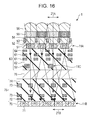
- FIG. 16 is a further cross-sectional configuration diagram of the solid-state imaging device 1 according to the second embodiment.
- the regions of a wiring layer 92 as the aperture 11 C are formed to be smaller than the regions of the wiring layer 91 of FIG. 15 .
- the incident light passing through the G pixels of the upper side substrate 11 A is also partially incident on the lower side substrate 11 B.
- the aperture 11 C may be formed by the glass layer 81 , and may be formed by the wiring layer 91 ( 92 ). However, it is preferable that the aperture 11 C be formed by the wiring layer 91 ( 92 ) in that it is possible to use precision of matching of the semiconductor process.
- FIG. 17 is a further cross-sectional configuration diagram of the solid-state imaging device 1 according to the second embodiment.
- a glass layer as an intermediate layer 93 is inserted to be interposed between the upper side substrate 11 A and the protective film 76 of the lower side substrate 11 B.
- the intermediate layer 93 is not limited to glass, and may be formed of a transparent material.
- a plurality of pixels 21 B is formed on the lower side substrate 11 B so as to correspond to only a part of the upper side substrate 11 A.
- a plurality of pixels 31 B as an exposure control detection sensor can be formed.
- exposure control is performed on the basis of an output level of a captured image.
- a luminance suddenly changes, a reading speed of an image is slow, and thus control for gradually shortening an exposure time period is performed.
- control for gradually shortening an exposure time period is performed.
- appropriate exposure is gradually performed, and thus a visually undesirable image may be obtained.
- an exposure control signal is detected by the plurality of pixels 31 B provided on the lower side substrate 11 B different from the image sensor of the upper side substrate 11 A.
- the driving can be performed by setting timing of exposure and reading of the plurality of exposure control pixels 31 B separately from the plurality of autofocus pixels 21 B. Therefore, it is possible to perform exposure control at a high speed, and thus it is possible to instantly perform appropriate exposure of the image sensor of the upper side substrate 11 A.
- FIG. 19 shows an example in which the pixel size of the lower side substrate 11 B is the same as the pixel size of the upper side substrate 11 A and thus the plurality of autofocus pixels 21 B and the plurality of exposure control pixels 31 B are arranged on the lower side substrate 11 B on a row-by-row basis.
- FIG. 20 shows an example in which the pixel size of the lower side substrate 11 B is set as the pitch of repetition of the color array of the color filters of the upper side substrate 11 A and thus the plurality of autofocus pixels 21 C and a plurality of exposure control pixels 31 C are arranged on a row-by-row basis.
- the contrast method is means which is effective near the focus position
- the image plane phase difference method is means which is effective at a location where the focus is significantly shifted.
- phase difference pixels may be additionally provided on a part of the upper side substrate 11 A.
- FIGS. 21 to 23 show examples in which phase difference pixels 101 are additionally provided on a part of the upper side substrate 11 A.
- FIG. 21 shows an example in which some of imaging pixels 21 A of the upper side substrate 11 A are formed as phase difference detection pixels 101 in the solid-state imaging device 1 where the pixel size of the lower side substrate 11 B is the same as the pixel size of the upper side substrate 11 A.
- the phase difference detection pixels 101 for example, two pixels 101 A and 101 B are symmetrically disposed such that light blocking regions are symmetric like a right-side light blocking region and a left-side light blocking region.
- FIG. 22 shows an example in which some of imaging pixels 21 A of the upper side substrate 11 A are formed as phase difference detection pixels 101 in the solid-state imaging device 1 where the pixel size of the lower side substrate 11 B is set as the pitch of repetition of the color array of the color filters of the upper side substrate 11 A.
- each phase difference detection pixel 101 a part of the pixel region is shielded from light. Therefore, the intensity of the light, which is incident on the lower side substrate 11 B, is weak, and is thus inappropriate for the signal for the contrast method.
- the pixel rows, in which the phase difference detection pixels 101 are disposed are shielded from light by the aperture 11 C, and a region, in which focus control is performed in the image plane phase difference method, and a region, in which focus control is performed in the contrast method, can be divided on a row-by-row basis.
- the method of dividing the region, in which focus control is performed in the image plane phase difference method, and the region, in which focus control is performed in the contrast method may be on a color-by-color basis shown in FIG. 23 other than a row-by-row basis shown in FIGS. 21 and 22 .
- the G signal has high resolution to the human eye, and the G signal is used as a luminance signal even in the signal processing. Therefore, it is preferable that the phase difference detection pixels 101 be disposed on the G pixels among the R, G, and B pixels. In such a case, as shown in FIG. 23 , it is necessary for the G pixels to be shielded from light by the aperture 11 C. However, in the second method of matching the spectroscopic properties, the G pixels are shielded from light. Therefore, the configuration of FIG. 23 is appropriate for the second method of matching the spectroscopic properties.
- the configuration of the solid-state imaging device 1 shown in FIG. 23 is most appropriate for hybrid type autofocus.
- focus control of the contrast method is performed by matching the spectroscopic properties through the second method, and focus control is performed through the phase difference detection.
- the G signal can also be used in focus control of the contrast method. Therefore, there is an advantage in that focus precision is high even in a dark scene. Further, the exposure reading timing is controlled on a row-by-row basis, and thus the plurality of exposure control pixels 31 B may be disposed on the lower side substrate 11 B.
- FIG. 24 is a diagram illustrating a solid-state imaging device 1 according to a third embodiment of the present disclosure.
- the solid-state imaging device 1 according to the third embodiment is, for example, a combination-type solid-state imaging device in which two semiconductor substrates (silicon substrates) 11 D and 11 E are laminated through an aperture 11 F.
- the semiconductor substrate 11 D close to the optical lens 2 is referred to as an upper side substrate 11 D
- the semiconductor substrate 11 E far from the optical lens 2 is referred to as a lower side substrate 11 E.
- the substrates are simply referred to as substrates 11 .
- FIG. 25 is a diagram illustrating a schematic configuration of the upper side substrate 11 D and the lower side substrate 11 E of the solid-state imaging device 1 .
- the plurality of pixels 21 A in which color filters of red (R), green (G), and blue (B) are formed, is arranged on the upper side substrate 11 D in a two-dimensional array shape.
- the color filters formed on the pixels 21 A of the upper side substrate 11 D are arranged in, for example, a Bayer array, in a similar manner to the first and second embodiments. Accordingly, the upper side substrate 11 D may function as a color image sensor that outputs R, G, and B color signals.
- the plurality of pixels 21 B is formed on the lower side substrate 11 E in a shape which corresponds to only some of a plurality of pixel rows formed on the upper side substrate 11 D. Contrary to the first and second embodiments, the plurality of pixels 21 B formed on the lower side substrate 11 E is used for phase difference detection. In a region in which the pixels 21 B of the lower side substrate 11 E are not formed, a logic circuit 22 B is formed, which includes a signal processing circuit that processes signals detected by the pixels 21 B of the lower side substrate 11 E.
- opening portions 111 are formed on the aperture 11 F with predetermined spacings.
- the incident light which passes through a single pixel (hereinafter referred to as a transmission pixel) of the upper side substrate 11 D corresponding to the opening portion 111 of the aperture 11 F, is incident on 4 pixels of 2 ⁇ 2 pixels of the lower side substrate 11 E.
- the pixels 21 B of the lower side substrate 11 E are the phase difference detection pixels. Therefore, the incident light, which passes through the transmission pixel of the upper side substrate 11 D, may be received by a plurality of pixels. For example, as shown in FIG. 27 , the light may be incident on 16 pixels of 4 ⁇ 4 pixels.
- FIGS. 26 and 27 are diagrams illustrating relationships between the transmission pixel of the upper side substrate 11 D and the light receiving pixels of the lower side substrate 11 E that receive the incident light from the transmission pixel.
- the scales of the pixel sizes of the upper side substrate 11 D and the lower side substrate 11 E are different.
- a light concentration point of the micro lens is ideally on the photodiode surface of the silicon layer, but practically deep inside the silicon layer.
- the light concentration point for imaging is different from the light concentration point for phase difference detection.
- the phase difference detection pixels are disposed on the lower side substrate 11 E. Therefore, even in a state where a curvature of the micro lens is optimized for the pixels 21 A of the upper side substrate 11 D for imaging, it is possible to maximize separation performance of the phase difference pixels.
- FIG. 28 is a cross-sectional configuration diagram of the solid-state imaging device 1 according to the third embodiment.
- the upper side substrate 11 D, the lower side substrate 11 E, and the aperture 11 F in FIG. 28 correspond to the upper side substrate 11 A, the lower side substrate 11 B, and the aperture 11 C of FIG. 15 .
- the corresponding elements are represented by the same reference numerals and signs, and thus only a configuration different from that of FIG. 15 will be hereinafter described.
- a transparent layer 131 which does not absorb light, is formed on the silicon layer 51 of the transmission pixel of the upper side substrate 11 D.
- the light originating from the object 3 is incident on the photodiodes 71 of the lower side substrate 11 E through the on-chip lens 56 , the color filters 55 , the transparent layer 131 , and the opening portion 111 of the aperture 11 F.
- the transparent layer 131 can be formed of, for example, SiO2, which is oxidized silicon (Si), or the like.
- the pixel signal of the pixel 21 A of the upper side substrate 11 D, in which the transparent layer 131 is formed, is obtained through interpolation between the pixel signals of adjacent pixels.
- the intensity is weak but is at the level at which light can be received. Therefore, the photodiode 52 may be provided without change.
- the aperture 11 F may be formed as the glass layer 81 on which the light blocking pattern 81 P is deposited.
- the upper side substrate 11 D and the lower side substrate 11 E are separated at an appropriate distance.
- points of view of the incident light which passes through the transmission pixel of the upper side substrate 11 D, can be increased from 4 pixels of 2 ⁇ 2 pixels such that the light is incident, in an area of 16 pixels of 4 ⁇ 4 pixels, on the lower side substrate 11 E.
- resolution in the distance direction is improved.
- the color array of the upper side substrate 11 D is the Bayer array
- the transmission pixels are disposed on the upper side substrate 11 D with a pixel pitch which is an even number times the pixel size, the pixels with the same color are formed as the transmission pixels.
- the transmission pixels are disposed on the upper side substrate 11 D with a pixel pitch which is an odd number times the pixel size, the color array of the transmission pixels is formed as the Bayer array. As a result, it is possible to obtain color information from the lower side substrate 11 E.
- FIG. 30 shows an example in which the transmission pixels are disposed at a 3-pixel pitch which is an odd number times the pixel size such that the incident light, which passes through one transmission pixel of the upper side substrate 11 D, is received by 36 pixels of 6 ⁇ 6 pixels on the lower side substrate 11 E.
- image information of the Bayer array in which 36 pixels of 6 ⁇ 6 pixels are arranged on a color-by-color basis, can be obtained from the lower side substrate 11 E. Therefore, by re-synthesizing signals obtained by the lower side substrate 11 E, a captured image may be generated.
- FIG. 31 shows an example in which the transmission pixels are disposed at a 6-pixel pitch which is an even number times the pixel size such that the incident light, which passes through one transmission pixel of the upper side substrate 11 D, is received by 36 pixels of 6 ⁇ 6 pixels on the lower side substrate 11 E.
- the transmission pixels of the upper side substrate 11 D are the G pixels, and thus the lower side substrate 11 E also receives all the G signals.
- the color pixel of the transmission pixel may be any one of the R, G, and B pixels. However, as described above, in terms of human sensitivity characteristics or the like, it is preferable that the transmission pixels be disposed on the G pixels so as to perform focus control.
- a logic circuit 22 B can be disposed in a redundant region in which the pixels 21 B for phase difference detection are not formed on the lower side substrate 11 E.
- an imaging apparatus having the solid-state imaging device 1 has an optical zooming function
- an incident angle of light is changed by an image height.
- the pixel region of the lower side substrate 11 E in which the light passing through the transmission pixels of the upper side substrate 11 D is received, is changed.
- FIG. 32 shows a state where a focal length is shortened compared with the state shown in FIG. 30
- FIG. 33 shows a state where a focal length is shortened compared with the state shown in FIG. 31 .
- the imaging apparatus having the solid-state imaging device 1 has the optical zooming function
- the pixel region of the lower side substrate 11 E is changed through optical zooming. Consequently, even when a redundant region is generated through thinning, since there is the redundant region, there may be advantages in that it is possible to cope with the change of the pixel region of the lower side substrate 11 E caused by optical zooming and thus it becomes easy to perform signal processing.
- the plurality of pixels 31 B as an exposure control detection sensor can be formed in a region in which the plurality of phase difference detection pixels 21 B of the lower side substrate 11 E is not formed.
- FIG. 35 shows an example in which a plurality of exposure control pixels 31 B is disposed in a configuration in which the incident light passing through one transmission pixel of the upper side substrate 11 D shown in FIG. 26 is incident on 4 pixels of 2 ⁇ 2 pixels of the lower side substrate 11 E.
- FIG. 36 shows an example in which a plurality of exposure control pixels 31 B is disposed in a configuration in which the incident light passing through one transmission pixel of the upper side substrate 11 D shown in FIG. 27 is incident on 16 pixels of 4 ⁇ 4 pixels of the lower side substrate 11 E.
- an exposure control signal is detected by the plurality of pixels 31 B provided on the lower side substrate 11 E different from the image sensor of the upper side substrate 11 D. Further, since the pixels 21 B and 31 B are driven on a row-by-row basis, the driving can be performed by setting timing of exposure and reading of the plurality of exposure control pixels 31 B separately from the plurality of phase difference detection pixels 21 B. Therefore, it is possible to perform exposure control at a high speed, and thus it is possible to instantly perform appropriate exposure of the image sensor of the upper side substrate 11 D.
- a plurality of pixels as a contrast focus detection sensor may be formed.
- hybrid type autofocus capable of performing focus control according to the contrast method and focus control according to the phase difference method.
- the focus control according to the contrast method is performed using the signal, which is obtained by the image sensor of the upper side substrate 11 D, and the signal which is obtained by the contrast focus detection sensor of the lower side substrate 11 E.
- the focus control according to the phase difference method is performed using the signal which is obtained by the plurality of phase difference detection pixels 21 B of the lower side substrate 11 E.
- both the contrast focus detection sensor and the exposure control detection sensor may be disposed.
- the plurality of pixels 21 A as an image generation detection sensor (image sensor) is disposed on the upper side substrate 11 D, but it is conceivable that, in some cases, a 2-dimensional image may not be necessary.
- a signal processing circuit 151 such as a logic circuit and a memory circuit, can be formed.
- the signal processing circuit 151 processes a phase difference detection signal obtained by the plurality of pixels 21 B of the lower side substrate 11 E.
- a micro lens array 163 is provided between a main lens 162 and an image sensor 164 , and the light originating from the object 161 is firstly imaged on the micro lens array 163 through the main lens 162 .
- micro lenses 171 are disposed with small gaps interposed between adjacent lenses.
- the spacing between the micro lens array 163 and the image sensor 164 is several mm, and thus it is difficult for the micro lenses 171 having large lens diameters to be formed in a semiconductor process. Further, the micro lenses 171 having large lens diameters are formed as a cemented lens, and thus the cementing management is difficult.
- each of on-chip lenses formed on the transmission pixels of the upper side substrate 11 D has a pixel size of an image sensor which can be manufactured in the semiconductor process.
- the spacing between the upper side substrate 11 D and the lower side substrate 11 E can be set as a distance which can be formed through bonding of the semiconductor substrates, and thus high precision alignment in the semiconductor process can be performed.
- the above-mentioned embodiments described a structure of the solid-state imaging device 1 in which the semiconductor substrate 11 A ( 11 D) having the silicon layer 51 as a photoelectric conversion layer and the semiconductor substrate 11 B ( 11 E) having the silicon layer 70 as a photoelectric conversion layer are laminated.
- the semiconductor substrate 11 A ( 11 D) and the semiconductor substrate 11 B ( 11 E) may be bonded in a wafer state, and may be bonded in a semiconductor chip state after dicing of the wafer.
- the laminated photoelectric conversion layer may be formed of, for example, a compound semiconductor having a chalcopyrite structure or an organic photoelectric conversion film. Further, the photoelectric conversion layer may be three or more laminated layers.
- the semiconductor substrate 11 A ( 11 D) is formed as a back side illumination type
- the semiconductor substrate 11 B ( 11 E) is formed as a front side illumination type.
- either one of the semiconductor substrate 11 A ( 11 D) and the semiconductor substrate 11 B ( 11 E) may be either one of the back side illumination type and the front side illumination type.
- FIGS. 40 to 42 elements corresponding to those of FIG. 28 are represented by the same reference numerals and signs, and thus a description thereof will be appropriately omitted.
- FIG. 40 is a cross-sectional configuration diagram of the solid-state imaging device 1 , in which both the upper side substrate 11 D and the lower side substrate 11 E are laminated as the front side illumination types, according to the third embodiment.
- the color filters 55 and the on-chip lens 56 are formed on the multilevel wiring layer 63 which is formed on the upper side of the silicon layer 51 having the photodiodes 52 formed therein.
- the wiring layer 91 as the aperture 11 F is formed on the back side of the silicon layer 51 , that is, a side thereof facing the lower side substrate 11 E.
- the wiring layer 91 is covered with a protective film 301 .
- the lower side substrate 11 E is also the front side illumination type
- the lower side substrate 11 E and the upper side substrate 11 D are bonded with the protective film 76 interposed therebetween such that the multilevel wiring layer 75 , which is formed on the upper side of the silicon layer 70 having the photodiodes 71 formed therein, faces the upper side substrate 11 D.
- FIG. 41 is a cross-sectional configuration diagram of the solid-state imaging device 1 , in which the upper side substrate 11 D is laminated as the front side illumination type and the lower side substrate 11 E is laminated as the back side illumination type, according to the third embodiment.
- the color filters 55 and the on-chip lens 56 are formed on the multilevel wiring layer 63 which is formed on the upper side of the silicon layer 51 having the photodiodes 52 formed therein.
- the wiring layer 91 as the aperture 11 F is formed on the back side of the silicon layer 51 , that is, a side thereof facing the lower side substrate 11 E.
- the wiring layer 91 is covered with the protective film 301 .
- the lower side substrate 11 E is the back side illumination type
- the lower side substrate 11 E and the upper side substrate 11 D are bonded with protective films 302 and 76 interposed therebetween such that a side of the lower side substrate 11 E opposite to the multilevel wiring layer 75 formed on the silicon layer 70 faces the upper side substrate 11 D.
- FIG. 42 is a cross-sectional configuration diagram of the solid-state imaging device 1 , in which both the upper side substrate 11 D and the lower side substrate 11 E are laminated as the back side illumination types, according to the third embodiment.
- the upper side substrate 11 D is the back side illumination type
- the light blocking film 53 , the planarizing film 54 , the color filters 55 , and the on-chip lens 56 are formed on the side (back side) of the upper side substrate 11 D opposite to the multilevel wiring layer 63 formed on the silicon layer 51 .
- the lower side substrate 11 E is also the back side illumination type
- the lower side substrate 11 E and the upper side substrate 11 D are bonded with the protective films 302 and 76 interposed therebetween such that a side of the lower side substrate 11 E opposite to the multilevel wiring layer 75 formed on the silicon layer 70 faces the upper side substrate 11 D.
- FIGS. 28 and 40 to 42 show all combinations of the front side illumination type or the back side illumination type in a case of bonding the upper side substrate 11 D and the lower side substrate 11 E.
- FIGS. 28 and 40 correspond to examples in which the incident light passing through the transmission pixel is incident on 4 pixels of 2 ⁇ 2 pixels of the lower side substrate 11 E as shown in FIG. 26 .
- FIGS. 41 and 42 correspond to examples in which the incident light passing through the transmission pixel is incident on 16 pixels of 4 ⁇ 4 pixels of the lower side substrate 11 E as shown in FIG. 27 .
- the wiring layers 61 also serve as a light blocking film, and thus the light blocking film 53 , which is provided in the case of the back side illumination type, is not necessary.
- the height (thickness) from the on-chip lens 56 to the aperture 11 F can be minimized, and thus a large amount of obliquely incident light, which is indicated by the arrow of the dashed line, is also received in the photodiodes 71 of the lower side substrate 11 E. That is, when the upper side substrate 11 D is formed as the front side illumination type, it is possible to improve properties of obliquely incident light.
- the transparent layer 131 which totally transmits the incident light, is formed in the region of the silicon layer 51 corresponding to the transmission pixel.
- the photodiode 52 may be provided without change as described above.
- the above-mentioned third embodiment described the example in which the G pixel is formed as the transmission pixel.
- the color pixel of the transmission pixel may be any one of the R pixel, the G pixel, and the B pixel.
- the G pixel be formed as the transmission pixel.
- the G pixels in the Bayer array are disposed in a checkered pattern form.
- the light which passes through one transmission pixel of the upper side substrate 11 D, is received by the plurality of pixels of the lower side substrate 11 E.
- the spacing between the transmission pixels of the upper side substrate 11 D is increased to correspond to the light receiving pixels of the lower side substrate 11 E.
- the G pixels are not entirely formed as the transmission pixels.
- the G pixels include G pixels (hereinafter referred to as Gr pixels) disposed in the same rows as the R and G pixels (hereinafter referred to as Gb pixels) disposed in the same rows as the B pixels.
- Gr pixels G pixels
- Gb pixels G pixels
- the Gr pixels are set as the transmission pixels.
- the opening portions 111 of the aperture 11 F are provided under the Gr pixels.
- the light, which is incident into the Gr pixels is transmitted to the lower side substrate 11 E, but the light, which is incident into the Gb pixels, is reflected by the aperture 11 F since the opening portions 111 are not formed below the Gb pixels. Consequently, there is a concern that there may be difference in light receiving characteristics between the Gr pixels and the Gb pixels in accordance with whether or not the aperture 11 F is present.
- the R pixels are formed as the transmission pixels, there is no concern that the difference in the light receiving characteristics may occur like the case where the G pixels are formed as the transmission pixels.
- FIGS. 44 and 45 show examples in which the R pixels are formed as the transmission pixels in the above-mentioned third embodiment.
- FIG. 44 shows an example in which the R pixels are formed as the transmission pixels and the incident light passing through the transmission pixels is incident on 4 pixels of 2 ⁇ 2 pixels of the lower side substrate 11 E.
- FIG. 45 shows an example in which the R pixels are formed as the transmission pixels and the incident light passing through the transmission pixels is incident on 16 pixels of 4 ⁇ 4 pixels of the lower side substrate 11 E.
- the arrangement spacing of the R pixels is larger than that of the G pixels.
- all the R pixels are formed as the transmission pixels, and thus it is possible to prevent the difference, which is problematic, in the light receiving characteristics between the same color pixels from occurring as in the G pixels.
- FIG. 46 is a cross-sectional configuration diagram illustrating a solid-state imaging device 1 according to a fourth embodiment of the present disclosure.
- the R pixels are formed as the transmission pixels.
- the silicon layer 51 of the transmission pixels of the upper side substrate 11 D instead of the transparent layer 131 , the photodiodes 52 are formed.
- a thickness of the silicon layer 51 in the fourth embodiment is formed to be less than a thickness thereof in the above-mentioned third embodiment.
- the photodiodes 52 are formed even in the R pixels as the transmission pixels of the upper side substrate 11 D, and the pixel signal can be acquired by all the pixels of the upper side substrate 11 D.
- the other configuration of the solid-state imaging device 1 of FIG. 46 is the same as the configuration thereof in the third embodiment, and a description thereof will be omitted.
- both the upper side substrate 11 D and the lower side substrate 11 E are formed as the back side illumination types, in a similar manner to the configuration of FIG. 42 of the third embodiment.
- FIGS. 47A and 47B show the light reception sensitivity of the solid-state imaging device 1 at a standard thickness where the standard thickness is a thickness of the silicon layer 51 in the above-mentioned third embodiment.
- FIG. 47A shows spectroscopic properties of the light which is incident on the upper side substrate 11 D and the lower side substrate 11 E at the standard thickness, similarly to FIGS. 5 and 6 .
- FIG. 47B shows integral sensitivities (relative sensitivities) of the R, G, and B pixels of the upper side substrate 11 D and the lower side substrate 11 E at the standard thickness.
- the integral sensitivity thereof corresponds to an area which is obtained by integrating the curve shown in Upper-R of FIG. 47A .
- an area of the light receiving surface of the lower side substrate 11 E is the same as an area of the light receiving surface of the upper side substrate 11 D. Accordingly, it may be said that the integral sensitivities are large enough for the light reception sensitivities which are obtained by the entire lower side substrate 11 E.
- the light reception sensitivity of the phase difference sensor of the lower side substrate 11 E in the third embodiment will be described.
- FIG. 48 shows a light receiving region 311 and a circuit region 312 of the lower side substrate 11 E having one chip size.
- the size of the light receiving region 311 is about 15.75 mm ⁇ 23.6 mm.
- FIG. 48 also shows a phase-difference-only sensor region 313 having the APS-C size, in a case of the method of generating the phase difference signal by the phase-difference-only sensor provided separately from the image sensor.
- an area of the light receiving region 311 of the lower side substrate 11 E for performing the phase difference detection is about 9 times an area of the phase-difference-only sensor region 313 .
- the thickness of the silicon layer 51 of the upper side substrate 11 D is set as the standard thickness. In this case, even when the photodiodes 52 are also provided in the transmission pixels of the upper side substrate 11 D and the light transmitted through the photodiodes 52 is made to be incident on the lower side substrate 11 E, it is possible to precisely perform the phase difference detection.
- FIGS. 49A and 49B show light reception sensitivities of the solid-state imaging device 1 , in which the silicon layer 51 of the upper side substrate 11 D is formed to be thin, according to the fourth embodiment.
- FIGS. 49A and 49B show an example in which the silicon layer 51 of the upper side substrate 11 D is formed to be thinner by about 25% than the standard thickness of the third embodiment.
- FIG. 49A shows spectroscopic properties of the light which is incident on the upper side substrate 11 D and the lower side substrate 11 E when the silicon layer 51 of the upper side substrate 11 D is formed to be thinner by about 25%.
- FIG. 49B shows integral sensitivities (relative sensitivities) of the R, G, and B pixels of the upper side substrate 11 D and the lower side substrate 11 E when the silicon layer 51 of the upper side substrate 11 D is formed to be thinner by about 25%.
- the integral sensitivities of the R, G, and B pixels of the upper side substrate 11 D are lowered compared with the case where the silicon layer 51 has the standard thickness.
- the integral sensitivities of the R, G, and B pixels of the lower side substrate 11 E become larger than that at the standard thickness.
- the light reception sensitivity of each pixel 21 B of the lower side substrate 11 E is greatly improved.
- the thickness of the silicon layer 51 of the upper side substrate 11 D it is possible to control the amount of light incident on the pixels 21 B of the lower side substrate 11 E.
- the solid-state imaging device 1 of the fourth embodiment while minimizing loss in the sensitivity of each pixel of the upper side substrate 11 D, it is possible to use all the pixels as the imaging sensor. Further, it is possible to precisely perform the phase difference detection in the lower side substrate 11 E.
- FIGS. 50A and 50B show configuration examples of circuit arrangement of the substrates 11 in a case where the solid-state imaging device 1 is configured to have a 2-layer structure of the upper side substrate 11 D and the lower side substrate 11 E.
- FIG. 50A shows a configuration example of circuit arrangement.
- a light receiving region 321 of the upper side substrate 11 D and a light receiving region 311 of the lower side substrate 11 E have the same sizes, and a coverage ratio of the phase difference sensor region of the lower side substrate 11 E to the light receiving region 321 of the upper side substrate 11 D is set to 100%.
- a circuit region 322 of the upper side substrate 11 D has the same size as a circuit region 312 of the lower side substrate 11 E.
- FIG. 50B shows a configuration example of circuit arrangement of the substrates 11 of the solid-state imaging device 1 in the case of the 2-layer structure in which a size of one chip is made to be as small as possible without deterioration in the light reception sensitivity of the image sensor.
- a light receiving region 331 as a phase difference sensor region and a circuit region 332 are formed on the lower side substrate 11 E.
- the respective circuits of the circuit region 322 of the upper side substrate 11 D and the circuit region 312 of the lower side substrate 11 E of FIG. 50A are disposed to be integrated in the circuit region 332 .
- a size of the circuit region 332 is greater than a size of the circuit region 312 of the lower side substrate 11 E in FIG. 50A .
- a coverage ratio of the phase difference sensor region of the lower side substrate 11 E to the light receiving region 321 of the upper side substrate 11 D it is possible to ensure at least 80%.
- FIG. 51 shows a configuration example of circuit arrangement of the substrates 11 in a case where the solid-state imaging device 1 is configured to have a multilayer structure of three substrates 11 .
- Only the light receiving region 321 is formed on an upper side substrate 11 G which is an uppermost layer of the 3-layer structure.
- a light receiving region 311 is formed on an intermediate substrate 11 H which is an intermediate layer.
- the light receiving region 311 has the same size as the light receiving region 321 , and is formed such that a coverage ratio of the phase difference sensor region of the intermediate substrate 11 H to the light receiving region 321 of the upper side substrate 11 G is 100%.
- a circuit region 341 is formed on a lower side substrate 11 J which is a lowermost layer of the 3-layer structure.
- the solid-state imaging device 1 As described above, by forming the solid-state imaging device 1 as the 3-layer structure, for example, it is possible to make a chip size thereof have the same size as APS-C and make the chip size smaller than the solid-state imaging device 1 having the 2-layer laminated structure of FIG. 50A . Further, it is possible to ensure a greater coverage ratio of the phase difference sensor region than that of the solid-state imaging device 1 having the 2-layer laminated structure of FIG. 50B .
- the whole of the lower side substrate 11 J as the lowermost layer is used as the circuit region 341 . Therefore, not only the driving circuit, which drives the pixels of the light receiving region 311 of the intermediate substrate 11 H and the light receiving region 321 of the upper side substrate 11 G, but also an analog-digital converter (ADC), a logic circuit, a memory, and the like can be disposed in the circuit region 341 of the lower side substrate 11 J.
- ADC analog-digital converter
- circuits are disposed on the lower side substrate 11 J of the lowermost layer so as to process signal processing of the image sensor of the uppermost layer and signal processing of the phase difference sensor of the intermediate layer in parallel, it is possible to improve a speed of detection of the phase difference autofocus.
- FIG. 52 shows a cross-sectional configuration diagram of the solid-state imaging device 1 in a case where the solid-state imaging device 1 is configured to have a multilayer structure of three substrates 11 .
- the upper side substrate 11 G and the intermediate substrate 11 H correspond to the upper side substrate 11 D and the lower side substrate 11 E of the solid-state imaging device 1 of the 2-layer laminated structure of FIG. 46 , and a description thereof will be omitted. Both the upper side substrate 11 G and the intermediate substrate 11 H are bonded to be the back side illumination types.
- the multilevel wiring layer 75 of the intermediate substrate 11 H and a multilevel wiring layer 374 of the lower side substrate 11 J are bonded through, for example, metallic bonding of Cu—Cu.
- the multilevel wiring layer 374 is formed of one or more wiring layers 372 and an interlayer insulation film 373 .
- Signal processing circuits including a plurality of transistors 371 are formed on a silicon layer 361 of the lower side substrate 11 J.
- the above-mentioned solid-state imaging device 1 can be applied to various electronic apparatuses of, for example, an imaging apparatus such as a digital still camera or a digital video camera, a mobile phone having an imaging function, and an audio player having an imaging function.
- FIG. 53 is a block diagram illustrating a configuration example of an imaging apparatus as an electronic apparatus according to an embodiment of the present disclosure.
- An imaging apparatus 201 shown in FIG. 53 includes an optical system 202 , a shutter apparatus 203 , a solid-state imaging device 204 , a control circuit 205 , a signal processing circuit 206 , a monitor 207 , and a memory 208 , and is able to capture a still image and a moving image.
- the optical system 202 is formed of a single lens or a plurality of lenses, guides light (incident light), which originates from an object, into the solid-state imaging device 204 , and forms an image on the light receiving surface of the solid-state imaging device 204 .
- the shutter apparatus 203 is disposed between the optical system 202 and the solid-state imaging device 204 , and controls a period of illumination of light and a period of blocking of light onto the solid-state imaging device 204 , under the control of the control circuit 205 .
- the solid-state imaging device 204 is formed by the above-mentioned solid-state imaging device 1 .
- the solid-state imaging device 204 accumulates signal charge, for a certain period of time, in response to light which is imaged on the light receiving surface through the optical system 202 and the shutter apparatus 203 .
- the signal charge accumulated in the solid-state imaging device 204 is transmitted in accordance with a driving signal (timing signal) which is supplied from the control circuit 205 .
- the solid-state imaging device 204 may be formed as a single chip by itself, and may be formed as a part of a camera module which is packaged together with the optical system 202 , the signal processing circuit 206 , and the like.
- the control circuit 205 outputs driving signals for controlling a transmission operation of the solid-state imaging device 204 and a shutter operation of the shutter apparatus 203 , and drives the solid-state imaging device 204 and the shutter apparatus 203 .
- the signal processing circuit 206 applies various kinds of signal processing to the pixel signal which is output from the solid-state imaging device 204 .
- An image (image data), which is obtained by the signal processing circuit 206 applying the signal processing, is supplied to and displayed on the monitor 207 , and is supplied to and stored (recorded) in the memory 208 .
- the solid-state imaging device 1 By using the solid-state imaging device 1 according to the above-mentioned embodiments as the solid-state imaging device 204 , it is possible to perform high speed and high precision autofocus and auto exposure. Accordingly, it is possible to achieve high image quality of a captured image also in the imaging apparatus 201 such as a video camera, a digital still camera, and a camera module for mobile apparatuses of a mobile phone and the like.
- the imaging apparatus 201 such as a video camera, a digital still camera, and a camera module for mobile apparatuses of a mobile phone and the like.
- each above-mentioned semiconductor region can be formed as a semiconductor region having an inverse conductive type.
- the technology of the present disclosure is not limited to being applied to the solid-state imaging device that detects distribution of the amount of incident visible light and captures the distribution as an image.
- the technology can be applied to most solid-state imaging devices, which capture an image of distribution of the amount of incidence of infrared rays, X rays, or particles, and solid-state imaging devices (physical amount distribution detection devices) such as a fingerprint detection sensor which detects distributions of other physical amounts such as a pressure and a capacitance and captures the distributions as images in a wider sense.
- a solid-state imaging device including two or more photoelectric conversion layers that have photoelectric conversion portions divided on a pixel-by-pixel basis and are laminated
- the solid-state imaging device in which focus control is performed by using a contrast difference between a signal, which is obtained by the first photoelectric conversion layer, and a signal, which is obtained by the second photoelectric conversion layer.
- the solid-state imaging device in which the signal, which is obtained by the first photoelectric conversion layer, is a color image signal, and the signal, which is obtained by the second photoelectric conversion layer, is a monochrome image signal.
- the solid-state imaging device according to any one of (1) to (3), in which a pixel size of a single pixel of the second photoelectric conversion layer is equal to a pitch of repetition of a color filter array of the first photoelectric conversion layer.
- the solid-state imaging device according to any one of (1) to (4), in which pixels, which detect the signal in the second photoelectric conversion layer, are predetermined color pixels of the first photoelectric conversion layer.
- the solid-state imaging device according to any one of (1) to (5), further including an intermediate layer that has different transmittances in accordance with colors of color filters of pixels of the first photoelectric conversion layer, and is interposed between the first photoelectric conversion layer and the second photoelectric conversion layer.
- the solid-state imaging device in which only pixels of red and blue color filters of the intermediate layer transmit light to the second photoelectric conversion layer.
- the solid-state imaging device according to any one of (2) to (7), in which a contrast difference of at least one of the signal, which is obtained by the first photoelectric conversion layer, and the signal, which is obtained by the second photoelectric conversion layer, is calculated using a signal which is obtained by performing weighted addition on signals of a plurality of pixels.
- the solid-state imaging device according to any one of (2) to (8), in which the pixels includes pixels which detect a phase difference.
- the solid-state imaging device in which the pixels which detect the phase difference are pixels of the first photoelectric conversion layer.
- the solid-state imaging device in which pixels, which detect the contrast difference, and the pixels, which detect the phase difference, are divided on a row-by-row basis.
- the solid-state imaging device in which pixels, which detect the contrast difference, and the pixels, which detect the phase difference, are divided for each color of color filters.
- the solid-state imaging device in which the pixels, which detect the phase difference, are green pixels.
- the plurality of pixels of the second photoelectric conversion layer includes at least pixels which detect the phase difference
- the solid-state imaging device in which a plurality of pixels of the first photoelectric conversion layer includes pixels, which transmit the light to the second photoelectric conversion layer, and pixels which do not transmit the light to the second photoelectric conversion layer.
- the solid-state imaging device according to (14) or (15), in which the light, which passes through an on-chip lens and color filters, is incident on the pixels which transmit the light to the second photoelectric conversion layer.
- the solid-state imaging device according to (14) or (16), in which instead of the photoelectric conversion portions, a layer, which does not absorb light, is formed on the pixels of the first photoelectric conversion layer which transmit the light to the second photoelectric conversion layer.
- the solid-state imaging device in which the light, which is incident into the single pixel of the first photoelectric conversion layer, is received by the photoelectric conversion portions of three or more pixels of the second photoelectric conversion layer in horizontal and vertical directions.
- the solid-state imaging device according to any one of (14) to (18), further including a light blocking layer, which does not transmit the light to the second photoelectric conversion layer.
- the solid-state imaging device in which the light blocking layer is a wiring layer.
- the solid-state imaging device in which the light blocking layer is a glass layer on which a pattern is deposited.
- the solid-state imaging device in which a position of a transistor circuit, which reads a signal obtained by the first photoelectric conversion layer, is different from a position of a transistor circuit, which reads a signal obtained by the second photoelectric conversion layer, in a planar direction.
- the solid-state imaging device according to any one of (1) to (22), in which the plurality of pixels of the second photoelectric conversion layer further includes pixels which control exposure.
- the solid-state imaging device according to any one of (1) to (23), in which a color filter array of the first photoelectric conversion layer is a Bayer array.
- the solid-state imaging device according to any one of (1) to (24), in which pixel rows of the second photoelectric conversion layer are arranged to correspond to only some of pixel rows of the first photoelectric conversion layer.
- the solid-state imaging device according to any one of (1) to (25), further including a transparent intermediate layer that is interposed between the first photoelectric conversion layer and the second photoelectric conversion layer.
- the solid-state imaging device according to any one of (1) to (26), in which a logic circuit is also formed on a substrate on which the second photoelectric conversion layer is formed.
- the solid-state imaging device in which a substrate, on which the second photoelectric conversion layer is formed, is a back side illumination type.
- the solid-state imaging device in which a substrate, on which the second photoelectric conversion layer is formed, is disposed on a side opposite to a side of the optical lens, and is bonded to a substrate on which a circuit is formed.
- An electronic apparatus including a solid-state imaging device in which two or more photoelectric conversion layers having photoelectric conversion portions divided on a pixel-by-pixel basis are laminated,
- a solid-state imaging device including:
- a photoelectric conversion layer that has photoelectric conversion portions divided on a pixel-by-pixel basis and is laminated
- the semiconductor substrate has a transmission pixel which corresponds to a single pixel of the photoelectric conversion layer and transmits light to the photoelectric conversion layer
- the light which is incident into the transmission pixel of the semiconductor substrate, is received by the photoelectric conversion portions of a plurality of pixels of the photoelectric conversion layer, and focus control is performed by using a phase difference which is obtained by the plurality of pixels of the photoelectric conversion layer.
Landscapes
- Engineering & Computer Science (AREA)
- Multimedia (AREA)
- Signal Processing (AREA)
- Physics & Mathematics (AREA)
- Spectroscopy & Molecular Physics (AREA)
- Human Computer Interaction (AREA)
- Solid State Image Pick-Up Elements (AREA)
- Transforming Light Signals Into Electric Signals (AREA)
- Measurement Of Optical Distance (AREA)
- Focusing (AREA)
- Automatic Focus Adjustment (AREA)
Abstract
Description
wU1=0.21G+0.5R (1), and
wL1=2g+r+b (2).
wU2=R (3)
wL2=3(r+b) (4)
Claims (30)
Applications Claiming Priority (4)
| Application Number | Priority Date | Filing Date | Title |
|---|---|---|---|
| JP2013-244952 | 2013-11-27 | ||
| JP2013244952 | 2013-11-27 | ||
| JP2014145101A JP2015128131A (en) | 2013-11-27 | 2014-07-15 | Solid state image sensor and electronic apparatus |
| JP2014-145101 | 2014-07-15 |
Publications (2)
| Publication Number | Publication Date |
|---|---|
| US20150146056A1 US20150146056A1 (en) | 2015-05-28 |
| US9686462B2 true US9686462B2 (en) | 2017-06-20 |
Family
ID=53182366
Family Applications (1)
| Application Number | Title | Priority Date | Filing Date |
|---|---|---|---|
| US14/549,300 Expired - Fee Related US9686462B2 (en) | 2013-11-27 | 2014-11-20 | Solid-state imaging device and electronic apparatus |
Country Status (3)
| Country | Link |
|---|---|
| US (1) | US9686462B2 (en) |
| JP (1) | JP2015128131A (en) |
| CN (1) | CN104681572B (en) |
Cited By (1)
| Publication number | Priority date | Publication date | Assignee | Title |
|---|---|---|---|---|
| US11178326B2 (en) | 2019-06-19 | 2021-11-16 | Samsung Electronics Co., Ltd. | Image sensor and electronic device including image sensor |
Families Citing this family (32)
| Publication number | Priority date | Publication date | Assignee | Title |
|---|---|---|---|---|
| JP2015088691A (en) * | 2013-11-01 | 2015-05-07 | ソニー株式会社 | Solid-state imaging device, manufacturing method thereof, and electronic apparatus |
| JP6392542B2 (en) * | 2014-05-08 | 2018-09-19 | オリンパス株式会社 | Solid-state imaging device |
| US10554874B2 (en) | 2014-07-22 | 2020-02-04 | Sony Semiconductor Solutions Corporation | Solid-state imaging device and electronic equipment |
| WO2016132950A1 (en) * | 2015-02-20 | 2016-08-25 | ソニー株式会社 | Image capturing device and image capturing method |
| JP2016191875A (en) * | 2015-03-31 | 2016-11-10 | 株式会社ニコン | Focus detection apparatus and photographing apparatus |
| WO2016194577A1 (en) * | 2015-05-29 | 2016-12-08 | ソニー株式会社 | Imaging element, imaging method, program, and electronic device |
| WO2016194620A1 (en) * | 2015-06-01 | 2016-12-08 | ソニーセミコンダクタソリューションズ株式会社 | Solid-state imaging device and electronic device |
| JP2017011002A (en) * | 2015-06-18 | 2017-01-12 | ソニー株式会社 | Imaging device and electronic device |
| JP6578834B2 (en) * | 2015-09-09 | 2019-09-25 | リコーイメージング株式会社 | Imaging device and imaging apparatus |
| JP6574655B2 (en) * | 2015-09-16 | 2019-09-11 | キヤノン株式会社 | Imaging apparatus and encoding method in imaging apparatus |
| JPWO2017068713A1 (en) * | 2015-10-23 | 2018-08-16 | オリンパス株式会社 | Solid-state imaging device and imaging device |
| JP2017084926A (en) * | 2015-10-27 | 2017-05-18 | ソニー株式会社 | Solid-state imaging device, manufacturing method, and electronic apparatus |
| JP2017123380A (en) * | 2016-01-06 | 2017-07-13 | ソニー株式会社 | Solid state imaging device and method of manufacturing the same, and electronic apparatus |
| WO2017126329A1 (en) * | 2016-01-21 | 2017-07-27 | ソニー株式会社 | Image capturing element and electronic device |
| JP6780662B2 (en) * | 2016-01-22 | 2020-11-04 | ソニー株式会社 | Light receiving device, control method, and electronic equipment |
| JP2017152658A (en) * | 2016-02-26 | 2017-08-31 | 株式会社ニコン | Imaging device and imaging apparatus |
| WO2017163435A1 (en) * | 2016-03-25 | 2017-09-28 | 株式会社ニコン | Light-receiving element array and light field recording apparatus |
| JP6837652B2 (en) * | 2016-07-26 | 2021-03-03 | 株式会社シグマ | Imaging device and signal processing method |
| JP2018093297A (en) * | 2016-11-30 | 2018-06-14 | キヤノン株式会社 | Photoelectric conversion device and imaging system |
| JP2018200423A (en) * | 2017-05-29 | 2018-12-20 | ソニーセミコンダクタソリューションズ株式会社 | Imaging apparatus and electronic device |
| JP2018200980A (en) | 2017-05-29 | 2018-12-20 | ソニーセミコンダクタソリューションズ株式会社 | IMAGING DEVICE, SOLID-STATE IMAGING ELEMENT, AND ELECTRONIC DEVICE |
| JP6920110B2 (en) * | 2017-06-13 | 2021-08-18 | ルネサスエレクトロニクス株式会社 | Solid-state image sensor and its manufacturing method |
| TWI832908B (en) * | 2018-10-17 | 2024-02-21 | 日商索尼半導體解決方案公司 | Solid-state imaging device, manufacturing method of solid-state imaging device, and electronic apparatus |
| JP7336206B2 (en) * | 2019-02-27 | 2023-08-31 | キヤノン株式会社 | Method for manufacturing photoelectric conversion device |
| KR102494086B1 (en) | 2019-08-23 | 2023-01-30 | 선전 구딕스 테크놀로지 컴퍼니, 리미티드 | Fingerprint detection device, method and electronic device |
| CN111133445B (en) * | 2019-08-23 | 2021-09-24 | 深圳市汇顶科技股份有限公司 | Fingerprint identification devices and electronic equipment |
| CN111328398B (en) * | 2019-08-23 | 2021-09-17 | 深圳市汇顶科技股份有限公司 | Fingerprint identification device and electronic equipment |
| CN111095285B (en) * | 2019-08-23 | 2021-09-17 | 深圳市汇顶科技股份有限公司 | Fingerprint identification device and electronic equipment |
| KR102610583B1 (en) | 2019-10-18 | 2023-12-05 | 선전 구딕스 테크놀로지 컴퍼니, 리미티드 | Fingerprint detection devices and electronic devices |
| JP7437957B2 (en) * | 2020-02-06 | 2024-02-26 | ソニーセミコンダクタソリューションズ株式会社 | Photodetector, solid-state imaging device, and electronic equipment |
| KR102889666B1 (en) * | 2020-11-20 | 2025-11-21 | 에스케이하이닉스 주식회사 | Image sensing device |
| TW202537460A (en) * | 2023-10-20 | 2025-09-16 | 日商索尼半導體解決方案公司 | Light detection device |
Citations (4)
| Publication number | Priority date | Publication date | Assignee | Title |
|---|---|---|---|---|
| JP2000292685A (en) | 1999-04-01 | 2000-10-20 | Olympus Optical Co Ltd | Image pick-up element |
| JP2001250931A (en) | 2000-03-07 | 2001-09-14 | Canon Inc | Solid-state imaging device and imaging system using the same |
| US20110234884A1 (en) * | 2010-03-26 | 2011-09-29 | Panasonic Corporation | Imaging device |
| US20120105696A1 (en) * | 2010-10-27 | 2012-05-03 | Sony Corporation | Solid-state imaging device, semiconductor device, manufacturing methods thereof, and electronic apparatus |
Family Cites Families (4)
| Publication number | Priority date | Publication date | Assignee | Title |
|---|---|---|---|---|
| JP4348118B2 (en) * | 2003-06-04 | 2009-10-21 | 富士フイルム株式会社 | Solid-state imaging device and imaging device |
| JP5097275B2 (en) * | 2008-10-28 | 2012-12-12 | パナソニック株式会社 | Imaging unit |
| JP5791571B2 (en) * | 2011-08-02 | 2015-10-07 | キヤノン株式会社 | Imaging device and imaging apparatus |
| JP2013187475A (en) * | 2012-03-09 | 2013-09-19 | Olympus Corp | Solid state imaging device and camera system |
-
2014
- 2014-07-15 JP JP2014145101A patent/JP2015128131A/en active Pending
- 2014-11-17 CN CN201410657961.XA patent/CN104681572B/en not_active Expired - Fee Related
- 2014-11-20 US US14/549,300 patent/US9686462B2/en not_active Expired - Fee Related
Patent Citations (4)
| Publication number | Priority date | Publication date | Assignee | Title |
|---|---|---|---|---|
| JP2000292685A (en) | 1999-04-01 | 2000-10-20 | Olympus Optical Co Ltd | Image pick-up element |
| JP2001250931A (en) | 2000-03-07 | 2001-09-14 | Canon Inc | Solid-state imaging device and imaging system using the same |
| US20110234884A1 (en) * | 2010-03-26 | 2011-09-29 | Panasonic Corporation | Imaging device |
| US20120105696A1 (en) * | 2010-10-27 | 2012-05-03 | Sony Corporation | Solid-state imaging device, semiconductor device, manufacturing methods thereof, and electronic apparatus |
Cited By (2)
| Publication number | Priority date | Publication date | Assignee | Title |
|---|---|---|---|---|
| US11178326B2 (en) | 2019-06-19 | 2021-11-16 | Samsung Electronics Co., Ltd. | Image sensor and electronic device including image sensor |
| US11563883B2 (en) | 2019-06-19 | 2023-01-24 | Samsung Electronics Co., Ltd. | Image sensor and electronic device including image sensor |
Also Published As
| Publication number | Publication date |
|---|---|
| CN104681572A (en) | 2015-06-03 |
| US20150146056A1 (en) | 2015-05-28 |
| CN104681572B (en) | 2019-02-15 |
| JP2015128131A (en) | 2015-07-09 |
Similar Documents
| Publication | Publication Date | Title |
|---|---|---|
| US9686462B2 (en) | Solid-state imaging device and electronic apparatus | |
| US9786714B2 (en) | Solid-state imaging element, method for manufacturing solid-state imaging element, and electronic device | |
| US12164116B2 (en) | Solid-state imaging device, method of manufacturing the same, and electronic apparatus | |
| US10498990B2 (en) | Imaging systems with high dynamic range and phase detection pixels | |
| US12317617B2 (en) | Solid-state imaging device and electronic equipment | |
| KR102523203B1 (en) | Solid state image sensor, method of manufacturing the same, and electronic device | |
| US9911768B2 (en) | Solid state imaging device and electronic apparatus | |
| US20170338265A1 (en) | Solid-state imaging device, manufacturing method thereof, and electronic apparatus | |
| JPWO2017169479A1 (en) | IMAGING ELEMENT AND IMAGING DEVICE | |
| KR102128467B1 (en) | Image sensor and image photograph apparatus including image sensor | |
| CN105280653B (en) | Image Sensor | |
| CN107077605A (en) | A kind of unit pixel and the fingerprint Identification sensor comprising it | |
| KR20150141035A (en) | Image sensor | |
| US10784300B1 (en) | Solid-state imaging devices | |
| KR100848945B1 (en) | Microlens Array Compensating Chief Ray and Image Sensor Assembly Having the Same | |
| WO2012066846A1 (en) | Solid-state image sensor and imaging device | |
| JP2015159231A (en) | Solid-state imaging device | |
| US20250254445A1 (en) | Image sensor |
Legal Events
| Date | Code | Title | Description |
|---|---|---|---|
| AS | Assignment |
Owner name: SONY CORPORATION, JAPAN Free format text: ASSIGNMENT OF ASSIGNORS INTEREST;ASSIGNOR:HIROTA, ISAO;REEL/FRAME:034386/0322 Effective date: 20141105 |
|
| STCF | Information on status: patent grant |
Free format text: PATENTED CASE |
|
| MAFP | Maintenance fee payment |
Free format text: PAYMENT OF MAINTENANCE FEE, 4TH YEAR, LARGE ENTITY (ORIGINAL EVENT CODE: M1551); ENTITY STATUS OF PATENT OWNER: LARGE ENTITY Year of fee payment: 4 |
|
| FEPP | Fee payment procedure |
Free format text: MAINTENANCE FEE REMINDER MAILED (ORIGINAL EVENT CODE: REM.); ENTITY STATUS OF PATENT OWNER: LARGE ENTITY |
|
| LAPS | Lapse for failure to pay maintenance fees |
Free format text: PATENT EXPIRED FOR FAILURE TO PAY MAINTENANCE FEES (ORIGINAL EVENT CODE: EXP.); ENTITY STATUS OF PATENT OWNER: LARGE ENTITY |
|
| STCH | Information on status: patent discontinuation |
Free format text: PATENT EXPIRED DUE TO NONPAYMENT OF MAINTENANCE FEES UNDER 37 CFR 1.362 |
|
| FP | Lapsed due to failure to pay maintenance fee |
Effective date: 20250620 |