US9685442B2 - Semiconductor device and method of manufacturing the same - Google Patents
Semiconductor device and method of manufacturing the same Download PDFInfo
- Publication number
- US9685442B2 US9685442B2 US14/885,308 US201514885308A US9685442B2 US 9685442 B2 US9685442 B2 US 9685442B2 US 201514885308 A US201514885308 A US 201514885308A US 9685442 B2 US9685442 B2 US 9685442B2
- Authority
- US
- United States
- Prior art keywords
- region
- impurity region
- impurity
- type impurity
- insulating film
- Prior art date
- Legal status (The legal status is an assumption and is not a legal conclusion. Google has not performed a legal analysis and makes no representation as to the accuracy of the status listed.)
- Active
Links
- 239000004065 semiconductor Substances 0.000 title claims abstract description 130
- 238000004519 manufacturing process Methods 0.000 title claims description 35
- 239000012535 impurity Substances 0.000 claims abstract description 350
- 239000000758 substrate Substances 0.000 claims abstract description 70
- 229910021332 silicide Inorganic materials 0.000 claims abstract description 65
- FVBUAEGBCNSCDD-UHFFFAOYSA-N silicide(4-) Chemical compound [Si-4] FVBUAEGBCNSCDD-UHFFFAOYSA-N 0.000 claims abstract description 65
- 229910052751 metal Inorganic materials 0.000 claims abstract description 63
- 239000002184 metal Substances 0.000 claims abstract description 63
- 238000000034 method Methods 0.000 claims description 46
- 239000010410 layer Substances 0.000 description 191
- 229920002120 photoresistant polymer Polymers 0.000 description 33
- 238000005468 ion implantation Methods 0.000 description 31
- 230000008569 process Effects 0.000 description 30
- XUIMIQQOPSSXEZ-UHFFFAOYSA-N Silicon Chemical compound [Si] XUIMIQQOPSSXEZ-UHFFFAOYSA-N 0.000 description 29
- 229910052710 silicon Inorganic materials 0.000 description 29
- 239000010703 silicon Substances 0.000 description 29
- 238000000206 photolithography Methods 0.000 description 27
- 230000001133 acceleration Effects 0.000 description 22
- 238000002955 isolation Methods 0.000 description 22
- VYPSYNLAJGMNEJ-UHFFFAOYSA-N Silicium dioxide Chemical compound O=[Si]=O VYPSYNLAJGMNEJ-UHFFFAOYSA-N 0.000 description 21
- 229910052814 silicon oxide Inorganic materials 0.000 description 21
- 230000004888 barrier function Effects 0.000 description 14
- -1 phosphorus ion Chemical class 0.000 description 14
- 229910052796 boron Inorganic materials 0.000 description 9
- KRHYYFGTRYWZRS-UHFFFAOYSA-N Fluorane Chemical compound F KRHYYFGTRYWZRS-UHFFFAOYSA-N 0.000 description 8
- 229910052581 Si3N4 Inorganic materials 0.000 description 7
- 239000011229 interlayer Substances 0.000 description 7
- HQVNEWCFYHHQES-UHFFFAOYSA-N silicon nitride Chemical compound N12[Si]34N5[Si]62N3[Si]51N64 HQVNEWCFYHHQES-UHFFFAOYSA-N 0.000 description 7
- 239000012298 atmosphere Substances 0.000 description 6
- 238000005530 etching Methods 0.000 description 6
- 238000005229 chemical vapour deposition Methods 0.000 description 5
- 238000001039 wet etching Methods 0.000 description 5
- MWUXSHHQAYIFBG-UHFFFAOYSA-N Nitric oxide Chemical compound O=[N] MWUXSHHQAYIFBG-UHFFFAOYSA-N 0.000 description 4
- 239000007864 aqueous solution Substances 0.000 description 4
- 229910052799 carbon Inorganic materials 0.000 description 4
- 229910017052 cobalt Inorganic materials 0.000 description 4
- 239000010941 cobalt Substances 0.000 description 4
- GUTLYIVDDKVIGB-UHFFFAOYSA-N cobalt atom Chemical compound [Co] GUTLYIVDDKVIGB-UHFFFAOYSA-N 0.000 description 4
- 230000006866 deterioration Effects 0.000 description 4
- 238000010586 diagram Methods 0.000 description 4
- 238000009826 distribution Methods 0.000 description 4
- 230000000694 effects Effects 0.000 description 4
- 238000010438 heat treatment Methods 0.000 description 4
- 230000003647 oxidation Effects 0.000 description 4
- 238000007254 oxidation reaction Methods 0.000 description 4
- 230000002265 prevention Effects 0.000 description 4
- 230000001681 protective effect Effects 0.000 description 4
- 229910015900 BF3 Inorganic materials 0.000 description 3
- OKTJSMMVPCPJKN-UHFFFAOYSA-N Carbon Chemical compound [C] OKTJSMMVPCPJKN-UHFFFAOYSA-N 0.000 description 3
- 229910001439 antimony ion Inorganic materials 0.000 description 3
- HAYXDMNJJFVXCI-UHFFFAOYSA-N arsenic(5+) Chemical compound [As+5] HAYXDMNJJFVXCI-UHFFFAOYSA-N 0.000 description 3
- WTEOIRVLGSZEPR-UHFFFAOYSA-N boron trifluoride Chemical compound FB(F)F WTEOIRVLGSZEPR-UHFFFAOYSA-N 0.000 description 3
- 238000009792 diffusion process Methods 0.000 description 3
- 230000006870 function Effects 0.000 description 3
- 239000012299 nitrogen atmosphere Substances 0.000 description 3
- 230000001590 oxidative effect Effects 0.000 description 3
- 229910052698 phosphorus Inorganic materials 0.000 description 3
- 239000011574 phosphorus Substances 0.000 description 3
- 229910021420 polycrystalline silicon Inorganic materials 0.000 description 3
- 238000004151 rapid thermal annealing Methods 0.000 description 3
- 230000000630 rising effect Effects 0.000 description 3
- ZOXJGFHDIHLPTG-UHFFFAOYSA-N Boron Chemical compound [B] ZOXJGFHDIHLPTG-UHFFFAOYSA-N 0.000 description 2
- NBIIXXVUZAFLBC-UHFFFAOYSA-N Phosphoric acid Chemical compound OP(O)(O)=O NBIIXXVUZAFLBC-UHFFFAOYSA-N 0.000 description 2
- NRTOMJZYCJJWKI-UHFFFAOYSA-N Titanium nitride Chemical compound [Ti]#N NRTOMJZYCJJWKI-UHFFFAOYSA-N 0.000 description 2
- 230000004913 activation Effects 0.000 description 2
- 230000008901 benefit Effects 0.000 description 2
- 230000002457 bidirectional effect Effects 0.000 description 2
- 238000001312 dry etching Methods 0.000 description 2
- 230000005684 electric field Effects 0.000 description 2
- 229910052732 germanium Inorganic materials 0.000 description 2
- GNPVGFCGXDBREM-UHFFFAOYSA-N germanium atom Chemical group [Ge] GNPVGFCGXDBREM-UHFFFAOYSA-N 0.000 description 2
- 239000011261 inert gas Substances 0.000 description 2
- 238000005259 measurement Methods 0.000 description 2
- 230000003071 parasitic effect Effects 0.000 description 2
- 238000001020 plasma etching Methods 0.000 description 2
- 238000001004 secondary ion mass spectrometry Methods 0.000 description 2
- 230000004075 alteration Effects 0.000 description 1
- 229910000147 aluminium phosphate Inorganic materials 0.000 description 1
- 230000015572 biosynthetic process Effects 0.000 description 1
- 230000015556 catabolic process Effects 0.000 description 1
- 230000005465 channeling Effects 0.000 description 1
- 230000009977 dual effect Effects 0.000 description 1
- 239000012467 final product Substances 0.000 description 1
- 238000005755 formation reaction Methods 0.000 description 1
- 238000011065 in-situ storage Methods 0.000 description 1
- 150000002500 ions Chemical class 0.000 description 1
- 230000008520 organization Effects 0.000 description 1
- 238000005268 plasma chemical vapour deposition Methods 0.000 description 1
- 238000005498 polishing Methods 0.000 description 1
- 239000000047 product Substances 0.000 description 1
- 230000009467 reduction Effects 0.000 description 1
- 239000000126 substance Substances 0.000 description 1
- 238000006467 substitution reaction Methods 0.000 description 1
- 239000002344 surface layer Substances 0.000 description 1
- 238000009279 wet oxidation reaction Methods 0.000 description 1
Images


Classifications
-
- H—ELECTRICITY
- H01—ELECTRIC ELEMENTS
- H01L—SEMICONDUCTOR DEVICES NOT COVERED BY CLASS H10
- H01L27/00—Devices consisting of a plurality of semiconductor or other solid-state components formed in or on a common substrate
- H01L27/02—Devices consisting of a plurality of semiconductor or other solid-state components formed in or on a common substrate including semiconductor components specially adapted for rectifying, oscillating, amplifying or switching and having at least one potential-jump barrier or surface barrier; including integrated passive circuit elements with at least one potential-jump barrier or surface barrier
- H01L27/04—Devices consisting of a plurality of semiconductor or other solid-state components formed in or on a common substrate including semiconductor components specially adapted for rectifying, oscillating, amplifying or switching and having at least one potential-jump barrier or surface barrier; including integrated passive circuit elements with at least one potential-jump barrier or surface barrier the substrate being a semiconductor body
- H01L27/08—Devices consisting of a plurality of semiconductor or other solid-state components formed in or on a common substrate including semiconductor components specially adapted for rectifying, oscillating, amplifying or switching and having at least one potential-jump barrier or surface barrier; including integrated passive circuit elements with at least one potential-jump barrier or surface barrier the substrate being a semiconductor body including only semiconductor components of a single kind
- H01L27/085—Devices consisting of a plurality of semiconductor or other solid-state components formed in or on a common substrate including semiconductor components specially adapted for rectifying, oscillating, amplifying or switching and having at least one potential-jump barrier or surface barrier; including integrated passive circuit elements with at least one potential-jump barrier or surface barrier the substrate being a semiconductor body including only semiconductor components of a single kind including field-effect components only
- H01L27/088—Devices consisting of a plurality of semiconductor or other solid-state components formed in or on a common substrate including semiconductor components specially adapted for rectifying, oscillating, amplifying or switching and having at least one potential-jump barrier or surface barrier; including integrated passive circuit elements with at least one potential-jump barrier or surface barrier the substrate being a semiconductor body including only semiconductor components of a single kind including field-effect components only the components being field-effect transistors with insulated gate
- H01L27/092—Devices consisting of a plurality of semiconductor or other solid-state components formed in or on a common substrate including semiconductor components specially adapted for rectifying, oscillating, amplifying or switching and having at least one potential-jump barrier or surface barrier; including integrated passive circuit elements with at least one potential-jump barrier or surface barrier the substrate being a semiconductor body including only semiconductor components of a single kind including field-effect components only the components being field-effect transistors with insulated gate complementary MIS field-effect transistors
- H01L27/0921—Means for preventing a bipolar, e.g. thyristor, action between the different transistor regions, e.g. Latchup prevention
-
- H—ELECTRICITY
- H01—ELECTRIC ELEMENTS
- H01L—SEMICONDUCTOR DEVICES NOT COVERED BY CLASS H10
- H01L21/00—Processes or apparatus adapted for the manufacture or treatment of semiconductor or solid state devices or of parts thereof
- H01L21/70—Manufacture or treatment of devices consisting of a plurality of solid state components formed in or on a common substrate or of parts thereof; Manufacture of integrated circuit devices or of parts thereof
- H01L21/77—Manufacture or treatment of devices consisting of a plurality of solid state components or integrated circuits formed in, or on, a common substrate
- H01L21/78—Manufacture or treatment of devices consisting of a plurality of solid state components or integrated circuits formed in, or on, a common substrate with subsequent division of the substrate into plural individual devices
- H01L21/82—Manufacture or treatment of devices consisting of a plurality of solid state components or integrated circuits formed in, or on, a common substrate with subsequent division of the substrate into plural individual devices to produce devices, e.g. integrated circuits, each consisting of a plurality of components
- H01L21/822—Manufacture or treatment of devices consisting of a plurality of solid state components or integrated circuits formed in, or on, a common substrate with subsequent division of the substrate into plural individual devices to produce devices, e.g. integrated circuits, each consisting of a plurality of components the substrate being a semiconductor, using silicon technology
- H01L21/8232—Field-effect technology
- H01L21/8234—MIS technology, i.e. integration processes of field effect transistors of the conductor-insulator-semiconductor type
- H01L21/8238—Complementary field-effect transistors, e.g. CMOS
- H01L21/823892—Complementary field-effect transistors, e.g. CMOS with a particular manufacturing method of the wells or tubs, e.g. twin tubs, high energy well implants, buried implanted layers for lateral isolation [BILLI]
-
- H—ELECTRICITY
- H01—ELECTRIC ELEMENTS
- H01L—SEMICONDUCTOR DEVICES NOT COVERED BY CLASS H10
- H01L27/00—Devices consisting of a plurality of semiconductor or other solid-state components formed in or on a common substrate
- H01L27/02—Devices consisting of a plurality of semiconductor or other solid-state components formed in or on a common substrate including semiconductor components specially adapted for rectifying, oscillating, amplifying or switching and having at least one potential-jump barrier or surface barrier; including integrated passive circuit elements with at least one potential-jump barrier or surface barrier
- H01L27/0203—Particular design considerations for integrated circuits
- H01L27/0248—Particular design considerations for integrated circuits for electrical or thermal protection, e.g. electrostatic discharge [ESD] protection
- H01L27/0251—Particular design considerations for integrated circuits for electrical or thermal protection, e.g. electrostatic discharge [ESD] protection for MOS devices
- H01L27/0255—Particular design considerations for integrated circuits for electrical or thermal protection, e.g. electrostatic discharge [ESD] protection for MOS devices using diodes as protective elements
-
- H—ELECTRICITY
- H01—ELECTRIC ELEMENTS
- H01L—SEMICONDUCTOR DEVICES NOT COVERED BY CLASS H10
- H01L27/00—Devices consisting of a plurality of semiconductor or other solid-state components formed in or on a common substrate
- H01L27/02—Devices consisting of a plurality of semiconductor or other solid-state components formed in or on a common substrate including semiconductor components specially adapted for rectifying, oscillating, amplifying or switching and having at least one potential-jump barrier or surface barrier; including integrated passive circuit elements with at least one potential-jump barrier or surface barrier
- H01L27/04—Devices consisting of a plurality of semiconductor or other solid-state components formed in or on a common substrate including semiconductor components specially adapted for rectifying, oscillating, amplifying or switching and having at least one potential-jump barrier or surface barrier; including integrated passive circuit elements with at least one potential-jump barrier or surface barrier the substrate being a semiconductor body
- H01L27/08—Devices consisting of a plurality of semiconductor or other solid-state components formed in or on a common substrate including semiconductor components specially adapted for rectifying, oscillating, amplifying or switching and having at least one potential-jump barrier or surface barrier; including integrated passive circuit elements with at least one potential-jump barrier or surface barrier the substrate being a semiconductor body including only semiconductor components of a single kind
- H01L27/085—Devices consisting of a plurality of semiconductor or other solid-state components formed in or on a common substrate including semiconductor components specially adapted for rectifying, oscillating, amplifying or switching and having at least one potential-jump barrier or surface barrier; including integrated passive circuit elements with at least one potential-jump barrier or surface barrier the substrate being a semiconductor body including only semiconductor components of a single kind including field-effect components only
- H01L27/088—Devices consisting of a plurality of semiconductor or other solid-state components formed in or on a common substrate including semiconductor components specially adapted for rectifying, oscillating, amplifying or switching and having at least one potential-jump barrier or surface barrier; including integrated passive circuit elements with at least one potential-jump barrier or surface barrier the substrate being a semiconductor body including only semiconductor components of a single kind including field-effect components only the components being field-effect transistors with insulated gate
- H01L27/092—Devices consisting of a plurality of semiconductor or other solid-state components formed in or on a common substrate including semiconductor components specially adapted for rectifying, oscillating, amplifying or switching and having at least one potential-jump barrier or surface barrier; including integrated passive circuit elements with at least one potential-jump barrier or surface barrier the substrate being a semiconductor body including only semiconductor components of a single kind including field-effect components only the components being field-effect transistors with insulated gate complementary MIS field-effect transistors
- H01L27/0928—Devices consisting of a plurality of semiconductor or other solid-state components formed in or on a common substrate including semiconductor components specially adapted for rectifying, oscillating, amplifying or switching and having at least one potential-jump barrier or surface barrier; including integrated passive circuit elements with at least one potential-jump barrier or surface barrier the substrate being a semiconductor body including only semiconductor components of a single kind including field-effect components only the components being field-effect transistors with insulated gate complementary MIS field-effect transistors comprising both N- and P- wells in the substrate, e.g. twin-tub
-
- H—ELECTRICITY
- H01—ELECTRIC ELEMENTS
- H01L—SEMICONDUCTOR DEVICES NOT COVERED BY CLASS H10
- H01L29/00—Semiconductor devices adapted for rectifying, amplifying, oscillating or switching, or capacitors or resistors with at least one potential-jump barrier or surface barrier, e.g. PN junction depletion layer or carrier concentration layer; Details of semiconductor bodies or of electrodes thereof ; Multistep manufacturing processes therefor
- H01L29/02—Semiconductor bodies ; Multistep manufacturing processes therefor
- H01L29/06—Semiconductor bodies ; Multistep manufacturing processes therefor characterised by their shape; characterised by the shapes, relative sizes, or dispositions of the semiconductor regions ; characterised by the concentration or distribution of impurities within semiconductor regions
- H01L29/0603—Semiconductor bodies ; Multistep manufacturing processes therefor characterised by their shape; characterised by the shapes, relative sizes, or dispositions of the semiconductor regions ; characterised by the concentration or distribution of impurities within semiconductor regions characterised by particular constructional design considerations, e.g. for preventing surface leakage, for controlling electric field concentration or for internal isolations regions
- H01L29/0607—Semiconductor bodies ; Multistep manufacturing processes therefor characterised by their shape; characterised by the shapes, relative sizes, or dispositions of the semiconductor regions ; characterised by the concentration or distribution of impurities within semiconductor regions characterised by particular constructional design considerations, e.g. for preventing surface leakage, for controlling electric field concentration or for internal isolations regions for preventing surface leakage or controlling electric field concentration
- H01L29/0611—Semiconductor bodies ; Multistep manufacturing processes therefor characterised by their shape; characterised by the shapes, relative sizes, or dispositions of the semiconductor regions ; characterised by the concentration or distribution of impurities within semiconductor regions characterised by particular constructional design considerations, e.g. for preventing surface leakage, for controlling electric field concentration or for internal isolations regions for preventing surface leakage or controlling electric field concentration for increasing or controlling the breakdown voltage of reverse biased devices
- H01L29/0615—Semiconductor bodies ; Multistep manufacturing processes therefor characterised by their shape; characterised by the shapes, relative sizes, or dispositions of the semiconductor regions ; characterised by the concentration or distribution of impurities within semiconductor regions characterised by particular constructional design considerations, e.g. for preventing surface leakage, for controlling electric field concentration or for internal isolations regions for preventing surface leakage or controlling electric field concentration for increasing or controlling the breakdown voltage of reverse biased devices by the doping profile or the shape or the arrangement of the PN junction, or with supplementary regions, e.g. junction termination extension [JTE]
- H01L29/0619—Semiconductor bodies ; Multistep manufacturing processes therefor characterised by their shape; characterised by the shapes, relative sizes, or dispositions of the semiconductor regions ; characterised by the concentration or distribution of impurities within semiconductor regions characterised by particular constructional design considerations, e.g. for preventing surface leakage, for controlling electric field concentration or for internal isolations regions for preventing surface leakage or controlling electric field concentration for increasing or controlling the breakdown voltage of reverse biased devices by the doping profile or the shape or the arrangement of the PN junction, or with supplementary regions, e.g. junction termination extension [JTE] with a supplementary region doped oppositely to or in rectifying contact with the semiconductor containing or contacting region, e.g. guard rings with PN or Schottky junction
-
- H—ELECTRICITY
- H01—ELECTRIC ELEMENTS
- H01L—SEMICONDUCTOR DEVICES NOT COVERED BY CLASS H10
- H01L29/00—Semiconductor devices adapted for rectifying, amplifying, oscillating or switching, or capacitors or resistors with at least one potential-jump barrier or surface barrier, e.g. PN junction depletion layer or carrier concentration layer; Details of semiconductor bodies or of electrodes thereof ; Multistep manufacturing processes therefor
- H01L29/02—Semiconductor bodies ; Multistep manufacturing processes therefor
- H01L29/06—Semiconductor bodies ; Multistep manufacturing processes therefor characterised by their shape; characterised by the shapes, relative sizes, or dispositions of the semiconductor regions ; characterised by the concentration or distribution of impurities within semiconductor regions
- H01L29/0603—Semiconductor bodies ; Multistep manufacturing processes therefor characterised by their shape; characterised by the shapes, relative sizes, or dispositions of the semiconductor regions ; characterised by the concentration or distribution of impurities within semiconductor regions characterised by particular constructional design considerations, e.g. for preventing surface leakage, for controlling electric field concentration or for internal isolations regions
- H01L29/0642—Isolation within the component, i.e. internal isolation
- H01L29/0649—Dielectric regions, e.g. SiO2 regions, air gaps
-
- H—ELECTRICITY
- H01—ELECTRIC ELEMENTS
- H01L—SEMICONDUCTOR DEVICES NOT COVERED BY CLASS H10
- H01L29/00—Semiconductor devices adapted for rectifying, amplifying, oscillating or switching, or capacitors or resistors with at least one potential-jump barrier or surface barrier, e.g. PN junction depletion layer or carrier concentration layer; Details of semiconductor bodies or of electrodes thereof ; Multistep manufacturing processes therefor
- H01L29/02—Semiconductor bodies ; Multistep manufacturing processes therefor
- H01L29/36—Semiconductor bodies ; Multistep manufacturing processes therefor characterised by the concentration or distribution of impurities in the bulk material
-
- H—ELECTRICITY
- H01—ELECTRIC ELEMENTS
- H01L—SEMICONDUCTOR DEVICES NOT COVERED BY CLASS H10
- H01L29/00—Semiconductor devices adapted for rectifying, amplifying, oscillating or switching, or capacitors or resistors with at least one potential-jump barrier or surface barrier, e.g. PN junction depletion layer or carrier concentration layer; Details of semiconductor bodies or of electrodes thereof ; Multistep manufacturing processes therefor
- H01L29/66—Types of semiconductor device ; Multistep manufacturing processes therefor
- H01L29/66007—Multistep manufacturing processes
- H01L29/66075—Multistep manufacturing processes of devices having semiconductor bodies comprising group 14 or group 13/15 materials
- H01L29/66083—Multistep manufacturing processes of devices having semiconductor bodies comprising group 14 or group 13/15 materials the devices being controllable only by variation of the electric current supplied or the electric potential applied, to one or more of the electrodes carrying the current to be rectified, amplified, oscillated or switched, e.g. two-terminal devices
- H01L29/6609—Diodes
- H01L29/66136—PN junction diodes
-
- H—ELECTRICITY
- H01—ELECTRIC ELEMENTS
- H01L—SEMICONDUCTOR DEVICES NOT COVERED BY CLASS H10
- H01L29/00—Semiconductor devices adapted for rectifying, amplifying, oscillating or switching, or capacitors or resistors with at least one potential-jump barrier or surface barrier, e.g. PN junction depletion layer or carrier concentration layer; Details of semiconductor bodies or of electrodes thereof ; Multistep manufacturing processes therefor
- H01L29/66—Types of semiconductor device ; Multistep manufacturing processes therefor
- H01L29/66007—Multistep manufacturing processes
- H01L29/66075—Multistep manufacturing processes of devices having semiconductor bodies comprising group 14 or group 13/15 materials
- H01L29/66083—Multistep manufacturing processes of devices having semiconductor bodies comprising group 14 or group 13/15 materials the devices being controllable only by variation of the electric current supplied or the electric potential applied, to one or more of the electrodes carrying the current to be rectified, amplified, oscillated or switched, e.g. two-terminal devices
- H01L29/6609—Diodes
- H01L29/66143—Schottky diodes
-
- H—ELECTRICITY
- H01—ELECTRIC ELEMENTS
- H01L—SEMICONDUCTOR DEVICES NOT COVERED BY CLASS H10
- H01L29/00—Semiconductor devices adapted for rectifying, amplifying, oscillating or switching, or capacitors or resistors with at least one potential-jump barrier or surface barrier, e.g. PN junction depletion layer or carrier concentration layer; Details of semiconductor bodies or of electrodes thereof ; Multistep manufacturing processes therefor
- H01L29/66—Types of semiconductor device ; Multistep manufacturing processes therefor
- H01L29/68—Types of semiconductor device ; Multistep manufacturing processes therefor controllable by only the electric current supplied, or only the electric potential applied, to an electrode which does not carry the current to be rectified, amplified or switched
- H01L29/76—Unipolar devices, e.g. field effect transistors
- H01L29/772—Field effect transistors
- H01L29/78—Field effect transistors with field effect produced by an insulated gate
- H01L29/7833—Field effect transistors with field effect produced by an insulated gate with lightly doped drain or source extension, e.g. LDD MOSFET's; DDD MOSFET's
-
- H—ELECTRICITY
- H01—ELECTRIC ELEMENTS
- H01L—SEMICONDUCTOR DEVICES NOT COVERED BY CLASS H10
- H01L29/00—Semiconductor devices adapted for rectifying, amplifying, oscillating or switching, or capacitors or resistors with at least one potential-jump barrier or surface barrier, e.g. PN junction depletion layer or carrier concentration layer; Details of semiconductor bodies or of electrodes thereof ; Multistep manufacturing processes therefor
- H01L29/66—Types of semiconductor device ; Multistep manufacturing processes therefor
- H01L29/86—Types of semiconductor device ; Multistep manufacturing processes therefor controllable only by variation of the electric current supplied, or only the electric potential applied, to one or more of the electrodes carrying the current to be rectified, amplified, oscillated or switched
- H01L29/861—Diodes
- H01L29/8613—Mesa PN junction diodes
-
- H—ELECTRICITY
- H01—ELECTRIC ELEMENTS
- H01L—SEMICONDUCTOR DEVICES NOT COVERED BY CLASS H10
- H01L29/00—Semiconductor devices adapted for rectifying, amplifying, oscillating or switching, or capacitors or resistors with at least one potential-jump barrier or surface barrier, e.g. PN junction depletion layer or carrier concentration layer; Details of semiconductor bodies or of electrodes thereof ; Multistep manufacturing processes therefor
- H01L29/66—Types of semiconductor device ; Multistep manufacturing processes therefor
- H01L29/86—Types of semiconductor device ; Multistep manufacturing processes therefor controllable only by variation of the electric current supplied, or only the electric potential applied, to one or more of the electrodes carrying the current to be rectified, amplified, oscillated or switched
- H01L29/861—Diodes
- H01L29/872—Schottky diodes
- H01L29/8725—Schottky diodes of the trench MOS barrier type [TMBS]
Definitions
- the embodiments discussed herein are directed to a semiconductor device and a method of manufacturing the same.
- Patent Literature 1 Japanese Laid-Open Patent Publication No. 2009-238982
- Patent Literature 2 Japanese Laid-Open Patent Publication No. 2001-168352
- Patent Literature 3 Japanese Laid-Open Patent Publication No. 2009-64977
- Patent Literature 4 Japanese Laid-Open Patent Publication No. 62-179142
- Patent Literature 5 Japanese Laid-Open Patent Publication No. 10-335679
- Patent Literature 6 Japanese Laid-Open Patent Publication No. 2012-174878
- a semiconductor device includes: a semiconductor device includes: an insulating film in a first region of a semiconductor substrate; a first impurity region of a first conductivity type and a second impurity region of the first conductivity type, each of the first impurity region and the second impurity region including a part located deeper than the insulating film, and the insulating film being sandwiched by the first impurity region and the second impurity region in planar view in the first region of the semiconductor substrate; a metal silicide film on the first impurity region and in Schottky junction with the first impurity region.
- the first impurity region contains a first impurity of the first conductivity type such that a peak of a concentration profile is deeper than a bottom of the insulating film.
- the second impurity region contains a second impurity of the first conductivity type, a concentration of the second impurity in the second impurity region being higher than a concentration of the first impurity in a part of the first impurity region shallower than the bottom of the insulating film.
- the first impurity region and the second impurity region are in contact with each other at a position deeper than the bottom of the insulating film.
- a method of manufacturing a semiconductor device includes: forming a first impurity region of a first conductivity type in a first region of a semiconductor substrate; forming a second impurity region of the first conductivity type in contact with the first impurity region in the first region of the semiconductor substrate; forming an insulating film that separates a surface of the first impurity region and a surface of the second impurity region to be shallower than the first impurity region and the second impurity region, and such that the first impurity region and the second impurity region are in contact with each other at a position deeper than a bottom of the insulating film in the first region of the semiconductor substrate; and forming a metal silicide film on the first impurity region and in Schottky junction with the first impurity region.
- a first impurity of the first conductivity type is doped such that a peak of a concentration profile is deeper than the bottom of the insulating film in the forming the first impurity region.
- a second impurity of the first conductivity type is doped such that a concentration of the second impurity in the second impurity region is higher than a concentration of the first impurity in a part of the first impurity region shallower than the bottom of the insulating film.
- FIGS. 1A and 1B are views illustrating a configuration of a reference example
- FIGS. 2A and 2B are views illustrating a configuration of a semiconductor device according to a first embodiment
- FIG. 3A to FIG. 3E are sectional views illustrating a method of manufacturing the semiconductor device according to the first embodiment in process sequence
- FIG. 4A and FIG. 4B are charts illustrating concentration profiles of an N-type impurity
- FIGS. 5A and 5B are views illustrating a configuration of a semiconductor device according to a second embodiment
- FIG. 6A and FIG. 6B are charts illustrating current-voltage characteristics
- FIGS. 7A to 7D are sectional views illustrating a configuration of a semiconductor device according to a third embodiment
- FIG. 8 is a circuit diagram illustrating a first example of a protection circuit
- FIG. 9 is a circuit diagram illustrating a second example of a protection circuit
- FIG. 10 is a circuit diagram illustrating a third example of a protection circuit
- FIG. 11 is a circuit diagram illustrating a fourth example of a protection circuit
- FIG. 12 a sectional view illustrating the fourth example of a protection circuit
- FIG. 13 is a sectional view illustrating a method of manufacturing the semiconductor device according to the third embodiment in process sequence
- FIGS. 14A to 14D are sectional views illustrating a method of manufacturing the semiconductor device according to the third embodiment in process sequence
- FIGS. 15A to 15D are sectional views illustrating a method of manufacturing the semiconductor device according to the third embodiment in process sequence
- FIGS. 16A to 16D are sectional views illustrating a method of manufacturing the semiconductor device according to the third embodiment in process sequence
- FIGS. 17A to 17D are sectional views illustrating a method of manufacturing the semiconductor device according to the third embodiment in process sequence
- FIGS. 18A to 18D are sectional views illustrating a method of manufacturing the semiconductor device according to the third embodiment in process sequence
- FIGS. 19A to 19D are sectional views illustrating a method of manufacturing the semiconductor device according to the third embodiment in process sequence
- FIGS. 20A to 20D are sectional views illustrating a method of manufacturing the semiconductor device according to the third embodiment in process sequence
- FIGS. 21A to 21D are sectional views illustrating a method of manufacturing the semiconductor device according to the third embodiment in process sequence
- FIGS. 22A to 22D are sectional views illustrating a method of manufacturing the semiconductor device according to the third embodiment in process sequence
- FIGS. 23A to 23D are sectional views illustrating a method of manufacturing the semiconductor device according to the third embodiment in process sequence
- FIGS. 24A to 24D are sectional views illustrating a method of manufacturing the semiconductor device according to the third embodiment in process sequence
- FIGS. 25A to 25D are sectional views illustrating a method of manufacturing the semiconductor device according to the third embodiment in process sequence
- FIGS. 26A to 26D are sectional views illustrating a method of manufacturing the semiconductor device according to the third embodiment in process sequence
- FIGS. 27A to 27D are sectional views illustrating a method of manufacturing the semiconductor device according to the third embodiment in process sequence
- FIGS. 28A to 28D are sectional views illustrating a method of manufacturing the semiconductor device according to the third embodiment in process sequence
- FIGS. 29A to 29D are sectional views illustrating a method of manufacturing the semiconductor device according to the third embodiment in process sequence
- FIGS. 30A to 30D are sectional views illustrating a method of manufacturing the semiconductor device according to the third embodiment in process sequence
- FIGS. 31A to 31D are sectional views illustrating a method of manufacturing the semiconductor device according to the third embodiment in process sequence
- FIGS. 32A to 32D are sectional views illustrating a method of manufacturing the semiconductor device according to the third embodiment in process sequence
- FIG. 33 is a chart illustrating a distribution of impurities in a reference example
- FIG. 34 is a chart illustrating a distribution of impurities in the third embodiment
- FIG. 35 is a view illustrating backward characteristics of an LRD
- FIGS. 36A to 36D are sectional views illustrating a configuration of a semiconductor device according to a fourth embodiment.
- FIGS. 37A to 37D are sectional views illustrating a method of manufacturing the semiconductor device according to the fourth embodiment in process sequence.
- FIGS. 38A to 38D are sectional views illustrating a method of manufacturing the semiconductor device according to the fourth embodiment in process sequence.
- FIGS. 39A to 39D are sectional views illustrating a method of manufacturing the semiconductor device according to the fourth embodiment in process sequence.
- FIGS. 1A and 1B are views illustrating a configuration of the reference example, where FIG. 1A is a plan view, and FIG. 1B is a sectional view along a I-I line in FIG. 1A .
- an N-well 316 is formed at a surface of a semiconductor substrate 301 such as a P-type silicon substrate.
- An insulating film 332 whose planar shape is annular is formed in the N-well 316 to be shallower than the N-well 316 .
- a metal silicide film 383 a is formed on a region of the N-well 316 surrounded by the insulating film 332 , and the N-well 316 is in Schottky contact with the metal silicide film 383 a .
- An N-type impurity layer 372 is formed at a surface of the N-well 316 at an outside of the insulating film 332 , and a metal silicide film 383 c is formed on the N-type impurity layer 372 .
- a concentration of an N-type impurity in the N-type impurity layer 372 is higher than that in the N-well 316 , and the N-type impurity layer 372 is in ohmic contact with the metal silicide film 383 c.
- the Schottky barrier diode of the reference example it may be possible to reduce a backward current for some extent, but the degree of reduction is not sufficient.
- An addition of process may be necessary to form the N-well whose N-type impurity concentration is low.
- various problems may be accompanied to simply reduce the N-type impurity concentration in the N-well 316 .
- the present inventors came up to the following embodiments as a result of hard study to reduce a backward current of a Schottky barrier diode while avoiding the above-stated various problems.
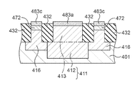
- FIGS. 2A and 2B are views illustrating a configuration of the semiconductor device according to the first embodiment, where FIG. 2A is a plan view, and FIG. 2B is a sectional view along a I-I line in FIG. 2A .
- an N-well 411 , and an N-well 416 surrounding the N-well 411 in planar view are formed at a surface of a semiconductor substrate 401 such as a P-type silicon substrate.
- a metal silicide film 483 a is formed on the N-well 411 , and the N-well 411 is in Schottky contact with metal silicide film 483 a .
- An N-type impurity layer 472 is formed at a surface of the N-well 416 , and a metal silicide film 483 c is formed on the N-type impurity layer 472 .
- a concentration of an N-type impurity in the N-type impurity layer 472 is higher than that in the N-well 416 , and the N-type impurity layer 472 is in ohmic contact with the metal silicide film 483 c .
- An insulating film 432 which insulates the metal silicide film 483 a and a part of the N-well 411 which is in Schottky contact with the metal silicide film 483 a from the metal silicide film 483 c and the N-type impurity layer 472 is formed between the N-well 411 and the N-well 416 .
- the insulating film 432 is formed to be shallower than the N-well 411 and the N-well 416 .
- a peak of a concentration profile of the N-type impurity contained in the N-well 411 is in a part of the N-well 411 deeper than a bottom of the insulating film 432 (deep part 412 ), and a concentration of the N-type impurity contained in the N-well 411 is lower as it approximates to a surface on a surface side of the peak.
- a concentration of the N-type impurity is extremely low in a shallow part 413 on the deep part 412 , and for example, it is less than 1.0 ⁇ 10 16 cm ⁇ 3 at a highest part.
- a maximum value of a concentration of the N-type impurity in the deep part 412 is, for example, over 1.0 ⁇ 10 16 cm ⁇ 3 .
- the N-well 416 is in contact with the deep part 412 on a lower side of the insulating film 432 .
- a concentration of the N-type impurity in the N-well 416 is higher than that in the shallow part 413 .
- a Schottky barrier diode including Schottky contact between the metal silicide film 483 a and the shallow part 413 of the N-well 411 is constituted.
- the concentration of the N-type impurity in the shallow part 413 is extremely low, and therefore, it is possible to reduce a backward current.
- the concentration of the N-type impurity in the deep part 412 is sufficiently high, and therefore, punch-through is difficult to occur, while the concentration of the N-type impurity in the shallow part 413 is extremely low, and it is possible to suppress deterioration of a backward withstand voltage due to punch-through.
- the peak of the concentration profile of the N-type impurity contained in the N-well 411 is in the deep part 412 , and therefore, it is possible to easily obtain the concentration profile in which the concentration of the N-type impurity in the shallow part 413 is extremely low and the concentration of the N-type impurity in the deep part 412 is sufficiently high.
- the deep part 412 whose concentration of the N-type impurity is sufficiently high is in contact with the N-well 416 on the lower side of the insulating film 432 , and therefore, parasitic resistance is low and it is possible to obtain excellent forward characteristics.
- FIG. 3A to FIG. 3E are sectional views illustrating the method of manufacturing the semiconductor device according to the first embodiment in process sequence.
- the N-well 411 is formed at the surface of the semiconductor substrate 401 by photolithography and ion-implantation. At this time, the N-well 411 is formed such that the peak of the concentration profile of the N-type impurity is deeper than the bottom of the insulating film 432 which is to be formed later.
- the concentration profile in a depth direction of the N-type impurity of the N-well 411 at this time is to be, for example, as illustrated in FIG. 4A .
- the concentration profile of the N-type impurity in a depth direction when an N-well 316 of the reference example is formed is illustrated in FIG. 4B for comparison. A dotted line in FIG.
- the concentration at the N-well 411 or 316 at an interface with the metal silicide film 483 a or 383 a it is extremely low such as approximately 1.0 ⁇ 10 14 cm ⁇ 3 in the embodiment, while it is high such as over 1.0 ⁇ 10 16 cm ⁇ 3 in the reference example.
- the large difference of the impurity concentrations leads to a large difference of backward current.
- the N-type impurity in the whole of the N-well 316 becomes insufficient.
- the N-well 416 which surrounds the N-well 411 in planar view is formed at the surface of the semiconductor substrate 401 by photolithography and ion-implantation.
- the N-well 416 may be formed to overlap with the N-well 411 .
- a trench which is shallower than the N-well 411 and the N-well 416 is formed along a boundary of the N-well 411 and the N-well 416 , and the insulating film 432 is formed in the trench.
- the N-well 411 may be defined into the deep part 412 which is deeper than the insulating film 432 and the shallow part 413 on the deep part 412 .
- the N-type impurity layer 472 is formed at the surface of the N-well 416 by photolithography and ion-implantation.
- the concentration of the N-type impurity in the N-type impurity layer 472 is higher than that in the N-well 416 .
- the metal silicide film 483 a is formed on the N-well 411
- the metal silicide film 483 c is formed on the N-type impurity layer 472 .
- the N-well 411 is in Schottky contact with the metal silicide film 483 a
- the N-type impurity layer 472 is ohmic contact with the metal silicide film 483 c.
- the semiconductor device according to the first embodiment can be manufactured.
- FIGS. 5A and 5B are views illustrating a configuration of the semiconductor device according to the second embodiment, where FIG. 5A is a plan view, and FIG. 5B is a sectional view along a I-I line in FIG. 5A .
- a P-type impurity layer 418 whose planar shape is annular is formed at a surface of the shallow part 413 as a guard ring.
- Other configurations are similar to the first embodiment.
- a Schottky barrier diode including the Schottky contact between the metal silicide film 483 a and the shallow part 413 of the N-well 411 and the P-type impurity layer 418 as the guard ring is constituted. It is also possible to obtain the similar effect as the first embodiment according to the second embodiment. Also, it is possible to further reduce a backward current by relaxation of electric field concentration compared to the first embodiment. It is possible to suppress deterioration of a backward withstand voltage due to punch-through, though the P-type impurity layer 418 is formed and the concentration of the N-type impurity in the shallow part 413 is low.
- FIG. 6A Current-voltage characteristics in the reference example and the first embodiment are illustrated in FIG. 6A
- FIG. 6B current-voltage characteristics in the second embodiment are illustrated in FIG. 6B .
- the backward current is lower in the first embodiment
- the backward current is further lower.
- the third embodiment relates to a semiconductor device including a DDC transistor, a high-voltage transistor, a low resistance diode (LRD), and a Schottky barrier diode (SBD).
- FIGS. 7A to 7D are sectional views illustrating a configuration of the semiconductor device according to the third embodiment.
- the DDC transistor has a large effect on suppressing variation of a threshold voltage due to statistical fluctuations of impurities, and it is effective for a high-speed transistor operating at a low voltage (for example, 0.9 V) used for a logic circuit or the like.
- a high-voltage NMOS transistor is a transistor where a high-voltage (for example, 3.3 V) compared to a driving voltage of the DDC transistor is applied, and it is used for, for example, 3.3 V I/O.
- the LRD is a PN junction diode, for example, and it is included for a surge protection, for example.
- the SBD is included for prevention of latch up of the DDC transistor, for example.
- the DDC-NMOS transistor 111 n is an N-channel type MOS transistor with DDC technology.
- the DDC-PMOS transistor 111 p is a P-channel type MOS transistor with DDC technology.
- the high-voltage NMOS transistor 112 n is an N-channel type MOS transistor which is driven by a higher voltage than the DDC-NMOS transistor 111 n .
- the high-voltage PMOS transistor 112 p is a P-channel type MOS transistor which is driven by a higher voltage than the DDC-PMOS transistor 111 p .
- a region 101 n in which the DDC-NMOS transistor 111 n is formed and a region 101 p in which the DDC-PMOS transistor 111 p is formed are included in the region 101 .
- a region 102 n in which the high-voltage NMOS transistor 112 n is formed and a region 102 p in which the high-voltage PMOS transistor 112 p is formed are included in the region 102 .
- the region 101 is illustrated in FIG. 7A
- the region 102 is illustrated in FIG. 7B
- the region 103 is illustrated in FIG. 7C
- the region 104 is illustrated FIG. 7D .
- a P-well 14 is formed at a surface of the semiconductor substrate 1 and an N-well 11 is formed under the P-well 14 in the region 101 n .
- An N-well 16 surrounding the P-well 14 from a lateral side is also formed.
- the P-well 14 is a double well surrounded from a lower side and a lateral side by the N-well 11 and the N-well 16 .
- a P-type impurity layer 15 is formed as a channel impurity layer (threshold voltage control layer) on the P-well 14 , and a non-doped epitaxial silicon layer 21 is formed on the P-type impurity layer 15 .
- a gate insulating film 52 is formed on the epitaxial silicon layer 21 , and a gate electrode 54 is formed on the gate insulating film 52 .
- a sidewall insulating film 56 is formed on a side surface of the gate electrode 54 .
- An N-type impurity layer 63 is formed as an extension region at a lower side of the sidewall insulating film 56 between the P-type impurity layer 15 and the gate insulating film 52 .
- An N-type impurity layer 65 in contact with the N-type impurity layer 63 and the P-type impurity layer 15 is formed to be deeper than the P-type impurity layer 15 on the outside of the sidewall insulating film 56 seen from the gate electrode 54 .
- Metal silicide films 81 are formed on the gate electrode 54 and on the N-type impurity layer 65 .
- the DDC-NMOS transistor 111 n including the N-type impurity layer 65 , the N-type impurity layer 63 , the P-type impurity layer 15 , the epitaxial silicon layer 21 , the gate insulating film 52 , the gate electrode 54 , and so on is formed in the region 101 n .
- the double well (the N-well 11 and the N-well 16 ) is included in the DDC-NMOS transistor 111 n , and therefore, it is possible to apply a back bias of a voltage different from a power supply voltage and a reference voltage on the DDC-NMOS transistor 111 n as it is described later.
- the N-well 16 is formed at the surface of the semiconductor substrate 1 in the region 101 p .
- An N-type impurity layer 17 is formed as a channel impurity layer (threshold voltage control layer) on the N-well 16 , the non-doped epitaxial silicon layer 21 is formed on the N-type impurity layer 17 .
- the gate insulating film 52 is formed on the epitaxial silicon layer 21 , and the gate electrode 54 is formed on the gate insulating film 52 .
- the sidewall insulating film 56 is formed on the side surface of the gate electrode 54 .
- a P-type impurity layer 64 is formed as an extension region at a lower side of the sidewall insulating film 56 between the N-type impurity layer 17 and the gate insulating film 52 .
- a P-type impurity layer 67 in contact with the P-type impurity layer 64 and the N-type impurity layer 17 is formed to be deeper than the N-type impurity layer 17 on the outside of the sidewall insulating film 56 seen from the gate electrode 54 .
- the metal silicide films 81 are formed on the gate electrode 54 and on the P-type impurity layer 67 .
- the DDC-PMOS transistor 111 p including the P-type impurity layer 67 , the P-type impurity layer 64 , the N-type impurity layer 17 , the epitaxial silicon layer 21 , the gate insulating film 52 , and the gate electrode 54 and so on is formed in the region 101 p.
- a P-well 41 is formed at the surface of the semiconductor substrate 1 in the region 102 n .
- a P-type impurity layer 42 is formed on the P-well 41
- a gate insulating film 53 thicker than the gate insulating film 52 is formed on the P-type impurity layer 42
- a gate electrode 55 is formed on the gate insulating film 53 .
- a gate length of the gate electrode 55 is larger than a gate length of the gate electrode 54 .
- the sidewall insulating film 56 is formed on a side surface of the gate electrode 55 .
- An N-type impurity layer 61 is formed as an LDD (lightly-doped drain) region at a lower side of the sidewall insulating film 56 at a surface of the P-type impurity layer 42 .
- An N-type impurity layer 66 in contact with the N-type impurity layer 61 and the P-type impurity layer 42 is formed to be deeper than the P-type impurity layer 42 on the outside of the sidewall insulating film 56 seen from the gate electrode 55 .
- the metal silicide films 81 are formed on the gate electrode 55 and on the N-type impurity layer 66 .
- the high-voltage NMOS transistor 112 n including the N-type impurity layer 66 , the N-type impurity layer 61 , the P-type impurity layer 42 , the gate insulating film 53 , the gate electrode 55 and so on is formed in the region 102 n.
- An N-well 43 is formed at the surface of the semiconductor substrate 1 in the region 102 p .
- An N-type impurity layer 44 is formed on the N-well 43 , the gate insulating film 53 thicker than the gate insulating film 52 is formed on the N-type impurity layer 44 , and the gate electrode 55 is formed on the gate insulating film 53 .
- the sidewall insulating film 56 is formed on the side surface of the gate electrode 55 .
- a P-type impurity layer 62 is formed as the LDD region at a lower side of the sidewall insulating film 56 at a surface of the N-type impurity layer 44 .
- a P-type impurity layer 68 in contact with the P-type impurity layer 62 and the N-type impurity layer 44 is formed to be deeper than the N-type impurity layer 44 on the outside of the sidewall insulating film 56 seen from the gate electrode 55 .
- the metal silicide films 81 are formed on the gate electrode 55 and on the P-type impurity layer 68 .
- the high-voltage PMOS transistor 112 p including the P-type impurity layer 68 , the P-type impurity layer 62 , the N-type impurity layer 44 , the gate insulating film 53 , the gate electrode 55 and so on is formed in the region 102 p.
- the P-well 14 is formed at the surface of the semiconductor substrate 1 , and the N-well 11 is formed under the P-well 14 , in the region 103 .
- the N-well 16 surrounding the P-well 14 from the lateral side is also formed.
- the P-well 14 is a double well surrounded from a lower side and a lateral side by the N-well 11 and the N-well 16 .
- An element isolation insulating film 32 is formed in the P-well 14 to be shallower than the P-well 14 , and a surface layer of the P-well 14 is defined to be two regions which are insulated from each other.
- An N-type impurity layer 71 is formed at a surface of the P-well 14 in one region, and a P-type impurity layer 73 is formed as a contact layer at the surface of the P-well 14 in the other region.
- a metal silicide film 82 c is formed as a cathode electrode on the N-type impurity layer 71
- a metal silicide film 82 a is formed as an anode electrode on the P-type impurity layer 73 .
- an PN junction diode including the P-well 14 and the N-type impurity layer 71 is formed as the LRD 113 in the region 103 .
- the N-well 11 , and the N-well 16 surrounding the N-well 11 in planar view are formed at the surface of the semiconductor substrate 1 in the region 104 .
- a metal silicide film 83 a is formed as an anode electrode on the N-well 11 , and the metal silicide film 83 a is in Schottky contact with the N-well 11 .
- An N-type impurity layer 72 is formed as a contact layer at a surface of the N-well 16 , and a metal silicide film 83 c is formed as a cathode electrode on the N-type impurity layer 72 .
- a concentration of the N-type impurity in the N-type impurity layer 72 is higher than that in the N-well 16 , and the metal silicide film 83 c is in ohmic contact with the N-type impurity layer 72 .
- the element isolation insulating film 32 which insulates the metal silicide film 83 a and a part of the N-well 11 which is in Schottky contact with the metal silicide film 83 a from the metal silicide film 83 c and the N-type impurity layer 72 is formed between the N-well 11 and the N-well 16 .
- the element isolation insulating film 32 is formed to be shallower than the N-well 11 and the N-well 16 .
- a peak of a concentration profile of the N-type impurity contained in the N-well 11 is in a part of the N-well 11 deeper than a bottom of the element isolation insulating film 32 (deep part 12 ), and a concentration of the N-type impurity contained in the N-well 11 is lower as it approximates to a surface on a surface side of the peak.
- a concentration of the N-type impurity is extremely low in a shallow part 13 on the deep part 12 , and for example, it is less than 1.0 ⁇ 10 16 cm ⁇ 3 at a highest part.
- a maximum value of a concentration of the N-type impurity in the deep part 12 is, for example, over 1.0 ⁇ 10 16 cm ⁇ 3 .
- the N-well 16 is in contact with the deep part 12 on a lower side of the element isolation insulating film 32 .
- a concentration of the N-type impurity in the N-well 16 is higher than that in the shallow part 13
- the concentration of the N-type impurity in the deep part 12 is higher than that in the N-well 16 .
- the SBD 114 including the N-well 11 , the metal silicide film 83 a , and the N-well 16 is formed in the region 104 .
- An interlayer insulating film 84 is formed over the semiconductor substrate 1 , and a conductive plug 85 , a conductive plug 86 a , a conductive plug 86 c , a conductive plug 87 a , a conductive plug 87 c , a wiring 88 , a wiring 89 a , a wiring 89 c , a wiring 90 a , and a wiring 90 c are formed in the interlayer insulating film 84 .
- the conductive plug 85 is in contact with the metal silicide film 81
- the wiring 88 is in contact with the conductive plug 85 .
- the conductive plug 86 a is in contact with the metal silicide film 82 a , and the wiring 89 a is in contact with the conductive plug 86 a .
- the conductive plug 86 c is in contact with the metal silicide film 82 c , and the wiring 89 c is in contact with the conductive plug 86 c .
- the conductive plug 87 a is in contact with the metal silicide film 83 a
- the wiring 90 a is in contact with the conductive plug 87 a .
- the conductive plug 87 c is in contact with the metal silicide film 83 c
- the wiring 90 c is in contact with the conductive plug 87 c.
- the concentration of the N-type impurity in the shallow part 13 is extremely low, and therefore, it is possible to reduce a backward current.
- the concentration of the N-type impurity in the deep part 12 is sufficiently high, and therefore, punch-through is difficult to occur, while the concentration of the N-type impurity in the shallow part 13 is extremely low, and it is possible to suppress deterioration of a the backward withstand voltage due to punch-through.
- the peak of the concentration profile of the N-type impurity contained in the N-well 11 is in the deep part 12 , and therefore, it is possible to easily obtain the concentration profile in which the concentration of the N-type impurity at the shallow part 13 is extremely low and the concentration of the N-type impurity in the deep part 12 is sufficiently high.
- the deep part 12 whose concentration of the N-type impurity is sufficiently high is in contact with the N-well 16 on the lower side of the element isolation insulating film 32 , and therefore, parasitic resistance is low and it is possible to obtain excellent forward characteristics.
- the LRD 113 and the SBD 114 are circuit elements constituting a protection circuit of the semiconductor device, and for example, as illustrated in FIG. 8 , they are inversely connected in parallel (inverse-parallel connection) between a VDD line and a VNW line, and between a VSS line and a VPW line.
- the VDD line is a power supply voltage line.
- the VSS line is a reference voltage line.
- the VNW line is a voltage line connected to the N-well 16 in the region 101 p , and a back-bias at a voltage different from the power supply voltage and the reference voltage is applied to the DDC-PMOS transistor 111 p via the VNW line.
- the VPW line is a voltage line connected to the P-well 14 in the region 101 n , and a back-bias at a voltage different from the power supply voltage and the reference voltage is applied to the DDC-NMOS transistor 111 n via the VPW line.
- the LRD 113 is a diode for surge protection, and in this example, the two LRDs 113 inversely connected in parallel constitute a bidirectional diode.
- the SBD 114 is a diode for latch-up prevention.
- a DDC transistor has a large effect on suppressing variation of the threshold voltage due to statistical fluctuations of impurities, but it is not possible to suppress variation of the threshold voltage between chips.
- the back-bias is applied to the DDC transistor, and thereby, it is possible to suppress the variation of the threshold voltage between chips, but a voltage different from the power supply voltage and the reference voltage is applied to a well, and therefore, a latch-up resistance resulting from noises such as a voltage inversion is lowered.
- the SBD 114 is connected between the VDD line and the VNW line, and between the VSS line and the VPW line, and therefore, it is possible to improve the latch-up resistance, and to reduce power consumption of the DDC-NMOS transistor 111 n and the DDC-PMOS transistor 111 p.
- FIG. 9 , FIG. 10 and FIG. 11 are views illustrating other examples of protection circuits including the LRD 113 and the SBD 114 .
- the SBD 114 serves also as the LRD 113 which is connected in the same direction as the SBD 114 in the example illustrated in FIG. 8 .
- the SBD 114 functions as a diode for latch-up prevention, and a parallel connected body of the LRD 113 and the SBD 114 functions as a bidirectional diode for surge protection.
- the LRD 113 which is connected in reverse to the SBD 114 in the example illustrated in FIG. 8 has a two-stage configuration.
- the LRD 113 which is connected in reverse to the SBD 114 in the example illustrated in FIG. 9 has the two-stage configuration.
- a stationary current may flow from the VNW line to the VDD line depending on a voltage applied to the VNW line, and a stationary current may flow from the VSS line to the VPW line depending on a voltage applied to the VPW line.
- a stationary current flows from the VSS line to the VPW line.
- a stationary current does not flow as long as the voltage does not exceed the double of the threshold voltage of the LRD 113 .
- the SBD 114 is not necessarily provided both of between the VDD line and the VNW line and between the VSS line and the VPW line, and the SBD 114 may be provided either one of them, for example, only in the protection circuit between the VSS line and the VPW line.
- a circuitry of the VSS line and the VPW line in the example illustrated in FIG. 11 may be enabled by connecting two pieces of LRDs 113 and the SBD 114 as, for example, illustrated in FIG. 12 .
- a SBD for latch-up prevention is sometimes manufactured as a discrete product, and is separately mounted on a circuit board where a semiconductor chip is mounted.
- the number of components increases to incur a cost increase.
- the latch-up may occur even though a Schottky barrier diode is mounted on the circuit board.
- the present inventors studied hard as for the problem, and it became clear that a loose connection of the semiconductor chip is a cause thereof. An operation test of the semiconductor chip is performed under a state in which the semiconductor chip is plugged in a socket formed on the circuit board, but when there is the loose connection between the socket and the semiconductor chip, the latch-up may occur even though the Schottky barrier diode is mounted.
- the SBD 114 is formed on the semiconductor substrate 1 which is in common with the DDC-NMOS transistor 111 n , the DDC-PMOS transistor 111 p , the high-voltage NMOS transistor 112 n and the high-voltage PMOS transistor 112 p , and therefore, the above-stated demerit which occurs when the SBD is prepared as an external component does not occur.
- FIG. 13 to FIG. 32 are sectional views illustrating the method of manufacturing the semiconductor device according to the third embodiment in process sequence.
- FIGS. 14A to 32A each illustrate the region 101
- FIGS. 14B to 32B each illustrate the region 102
- FIGS. 14C to 32C each illustrate the region 103
- FIGS. 14D to 32D each illustrate the region 104 .
- the region 101 where the DDC transistor is to be formed, the region 102 where the high-voltage transistor is to be formed, the region 103 where the PN junction diode is to be formed, and the region 104 where the Schottky barrier diode is to be formed are set at the semiconductor substrate 1 such as a silicon substrate.
- the region 101 n where the DDC-NMOS transistor is to be formed and the region 101 p where the DDC-PMOS transistor is to be formed are set in the region 101
- the region 102 n where the high-voltage NMOS transistor is to be formed and the region 102 p where the high-voltage PMOS transistor is to be formed are set in the region 102 .
- an alignment mark 2 is formed at the surface of the semiconductor substrate 1 .
- the alignment mark 2 is formed, for example, a region where the alignment mark 2 is to be formed is exposed by photolithography, a photoresist film covering the other regions is formed on the semiconductor substrate 1 , and the semiconductor substrate 1 is etched using the photoresist film as a mask. Then, the photoresist film is removed by asking, for example. Thereafter, a protective film 3 is formed on the surface of the semiconductor substrate 1 .
- a silicon oxide film is formed by, for example, a thermal oxidation method.
- the alignment mark 2 is formed in a region which is not included in a final product of the semiconductor substrate 1 such as, for example, a scribe region.
- a photoresist film 201 exposing the region 101 n , a region where the PN junction is to be formed in the region 103 , and a region where the Schottky junction is to be formed in the region 104 , and covering the other regions such as the region 101 p and the region 102 is formed on the semiconductor substrate 1 by photolithography.
- the alignment mark 2 is used for alignment of the photolithography.
- the N-well 11 is formed at the surface of the semiconductor substrate 1 in the region 101 n , the region 103 and the region 104 by doping of impurities using the photoresist film 201 as a mask.
- the N-well 11 is formed such that the peak of the concentration profile of the N-type impurity is deeper than the bottom of the element isolation insulating film 32 formed later.
- ion-implantation of phosphorus ion (P + ) is performed with the acceleration energy at 700 keV, and the dose amount at 1.5 ⁇ 10 13 cm ⁇ 2 , for example.
- the photoresist film 201 is removed by asking, for example.
- a photoresist film 202 exposing the region 101 n and the region where the PN junction is to be formed in the region 103 , and covering the other regions such as the region 101 p , the region 102 and the region 104 is formed on the semiconductor substrate 1 by photolithography.
- the alignment mark 2 is used for alignment of the photolithography.
- the P-well 14 and the P-type impurity layer 15 are formed at a part of the N-well 11 in the region 101 n and the region 103 by doping of impurities using the photoresist film 202 as a mask.
- ion-implantation of boron ion (B + ) is performed from four directions inclined relative to a substrate normal direction with the acceleration energy at 135 keV and the dose amount at 1.0 ⁇ 10 13 cm ⁇ 2 , for example.
- ion-implantation of germanium ion (Ge + ) is performed with the acceleration energy at 30 keV and the dose amount at 5 ⁇ 10 14 cm ⁇ 2
- ion-implantation of carbon ion (C + ) is performed with the acceleration energy at 5 keV and the dose amount at 5 ⁇ 10 14 cm ⁇ 2
- ion-implantation of the boron ion is performed with the acceleration energy at 10 keV and the dose amount at 1.8 ⁇ 10 13 cm ⁇ 2
- ion-implantation of boron fluoride ion (BF 2 + ) is performed with the acceleration energy at 25 keV and the dose amount at 6 ⁇ 10 12 cm ⁇ 2
- ion-implantation of the boron fluoride ion (BF 2 + ) is performed with the acceleration energy at 10 keV and the dose amount at 2.3 ⁇ 10 12 cm ⁇ 2 , for example.
- Germanium functions to prevent channeling of the boron ion by amorphousizing the semiconductor substrate 1 , and to increase probability in which carbon is disposed at a lattice point by amorphousizing the semiconductor substrate 1 .
- the carbon disposed at the lattice point functions to suppress diffusion of boron.
- germanium is ion-implanted prior to carbon and boron.
- the P-well 14 is desirably formed prior to the P-type impurity layer 15 .
- a photoresist film 203 exposing a region around the P-well 14 , a region around the N-well 11 , and the region 101 p , and covering the other regions such as the region 102 , the region where the P-well 14 exists, and the region where the N-well 11 exists is formed on the semiconductor substrate 1 by photolithography.
- the alignment mark 2 is used for alignment of the photolithography.
- the N-well 16 and the N-type impurity layer 17 are formed at the surface of the semiconductor substrate 1 in the region 101 n , the region 101 p , the region 103 and the region 104 by doping of impurities with the photoresist film 203 as a mask.
- ion-implantation of the phosphorous ion is performed from the four directions inclined relative to the substrate normal direction with the acceleration energy at 330 keV and the dose amount at 7.5 ⁇ 10 12 cm ⁇ 2
- ion-implantation of antimony ion (Sb + ) is performed with the acceleration energy at 80 keV and the dose amount at 1.2 ⁇ 10 13 cm ⁇ 2
- ion-implantation of the antimony ion is performed with the acceleration energy at 130 keV and the dose amount at 6 ⁇ 10 12 cm ⁇ 2 , for example.
- the N-type impurity layer 17 When the N-type impurity layer 17 is formed, ion-implantation of the antimony ion is performed with the acceleration energy at 20 keV and the dose amount at 6 ⁇ 10 12 cm ⁇ 2 , for example. Then, the photoresist film 203 is removed by asking, for example.
- a heat treatment is performed in an inert atmosphere, and thereby, damages generated in the semiconductor substrate 1 during the ion-implantations are recovered, and the implanted ions are activated.
- an atmosphere is a nitrogen atmosphere
- a substrate temperature is 600° C.
- a time period is 150 seconds.
- the protective film 3 is removed.
- the protective film 3 may be removed by wet etching using a hydrofluoric acid aqueous solution, for example.
- the non-doped epitaxial silicon layer 21 is formed on the semiconductor substrate 1 .
- the epitaxial silicon layer 21 may be formed by a chemical vapor deposition (CVD) method, and a thickness thereof is 25 nm, for example.
- a silicon oxide film 22 is formed over a surface of the epitaxial silicon layer 21 , and a silicon nitride film 23 is formed over the silicon oxide film 22 .
- the silicon oxide film 22 may be formed by wet oxidizing a surface of the epitaxial silicon layer 21 under a reduced pressure by an ISSG (in-situ steam generation) oxidation method, for example, and a thickness thereof is 3 nm, for example.
- a substrate temperature is 810° C.
- a time period is 20 seconds.
- the silicon nitride film 23 may be formed by a reduced pressure CVD method, for example, and a thickness thereof is 80 nm, for example.
- a substrate temperature is 700° C., and a time period is 150 minutes.
- a photoresist film 204 exposing an element isolation region is formed on the silicon nitride film 23 by photolithography.
- the alignment mark 2 is used for alignment of the photolithography.
- an element isolation trench 31 is formed in the element isolation region.
- the anisotropic etching of the silicon nitride film 23 , the silicon oxide film 22 , the epitaxial silicon layer 21 , and the semiconductor substrate 1 is performed using the photoresist film 204 as a mask. In this anisotropic etching, for example, dry etching is performed.
- the photoresist film 204 is removed by asking, for example.
- the element isolation insulating film 32 is formed in the element isolation trenche 31 .
- a silicon oxide film with a thickness of, for example, 10 nm is formed as a liner film at an inner surface of the element isolation trench 31 by thermally oxidizing the surfaces of the epitaxial silicon layer 21 and the semiconductor substrate 1 .
- a substrate temperature at this time is 650° C., for example.
- a silicon oxide film with a thickness of, for example, 475 nm is deposited by, for example, a high-density plasma CVD method, to thereby embed the element isolation trench 31 with the silicon oxide film 31 .
- a silicon oxide film on the silicon nitride film 23 is removed by, for example, a chemical mechanical polishing (CMP) method.
- CMP chemical mechanical polishing
- the element isolation insulating film 32 is etched for, for example, approximately 50 nm by wet etching using the hydrofluoric acid aqueous solution with the silicon nitride film 23 as a mask, for example.
- a height of the surface of the epitaxial silicon layer 21 and a height of the surface of the element isolation insulating film 32 become nearly equal by this etching under a state when the semiconductor device is completed.
- the silicon nitride film 23 is removed by wet etching using hot phosphoric acid, for example.
- a photoresist film 205 exposing the region 102 n and covering the other regions such as the region 101 , the region 102 p , the region 103 , and the region 104 is formed on the silicon oxide film 22 and the element isolation insulating film 32 by photolithography.
- the alignment mark 2 is used for alignment of the photolithography.
- the P-well 41 is formed in the semiconductor substrate 1
- the P-type impurity layer 42 is formed in the semiconductor substrate 1 and the epitaxial silicon layer 21 in the region 102 n by doping of impurities using the photoresist film 205 as a mask.
- ion-implantation of the boron ion is performed from four directions inclined relative to a substrate normal direction with the acceleration energy at 150 keV and the dose amount at 7.5 ⁇ 10 12 cm ⁇ 2 , for example.
- ion-implantation of the boron fluoride ion is performed with the acceleration energy at 5 keV and the dose amount at 3.2 ⁇ 10 12 cm ⁇ 2 , for example. Then, the photoresist film 205 is removed by asking, for example.
- a photoresist film 206 exposing the region 102 p and covering the other regions such as the region 101 , the region 102 n , the region 103 , and the region 104 is formed on the silicon oxide film 22 and the element isolation insulating film 32 by photolithography.
- the alignment mark 2 is used for alignment of the photolithography.
- the N-well 43 is formed in the semiconductor substrate 1
- the N-well 43 and the N-type impurity layer 44 are formed in the semiconductor substrate 1 and the epitaxial silicon layer 21 in the region 102 p by doping of impurities using the photoresist film 206 as a mask.
- the N-well 43 When the N-well 43 is formed, ion-implantation of the phosphorus ion is performed from four directions inclined relative to the substrate normal direction with the acceleration energy at 360 keV and the dose amount at 7.5 ⁇ 10 12 cm ⁇ 2 , for example.
- the N-type impurity layer 44 When the N-type impurity layer 44 is formed, ion-implantation of arsenic ion (As + ) is performed with the acceleration energy at 100 keV and the dose amount at 1.2 ⁇ 10 12 cm ⁇ 2 , for example. Then, the photoresist film 206 is removed by asking, for example.
- the N-well 43 may be formed instead of a part of the N-well 16 which constitutes the double well by surrounding the P-well 14 .
- the silicon oxide film 22 is removed.
- the silicon oxide film 22 may be removed by wet etching using the hydrofluoric acid aqueous solution, for example.
- a silicon oxide film 51 is formed on the surface of the epitaxial silicon film 21 .
- the silicon oxide film 51 may be formed by thermally oxidizing the surface of the epitaxial silicon layer 21 under the wet atmosphere, for example, and a thickness thereof is 7 nm, for example.
- a substrate temperature is 750° C., and a time period is 52 minutes.
- a photoresist film 207 covering the region 102 and exposing the other regions such as the region 101 , the region 103 , and the region 104 is formed on the silicon oxide film 51 .
- the silicon oxide film 51 is removed in the region 101 , the region 103 , and the region 104 by etching using the photoresist film 207 as a mask.
- the silicon oxide film 51 may be removed by the wet etching using the hydrofluoric acid aqueous solution, for example.
- the photoresist film 207 is removed by asking, for example.
- a gate insulating film 52 is formed at the surface of the epitaxial silicon layer 21 in each of the region 101 , the region 103 , and the region 104 , and a gate insulating film 53 is formed by additional oxidation of the silicon oxide film 51 in the region 102 .
- the gate insulating film 52 and the gate insulating film 53 are formed, for example, wet oxidation under the reduced pressure by the ISSG oxidation method is performed, and heat treatment is performed in the nitrogen monoxide (NO) atmosphere at a temperature of 870° C. for 13 seconds.
- a thickness of the gate insulating film 52 is 2 nm, for example.
- a gate electrode 54 is formed on the gate insulating film 52 in each of the region 101 n and the region 101 p , and a gate electrode 55 is formed on the gate insulating film 53 in each of the region 102 n and the region 102 p .
- a non-doped polycrystalline silicon film with a thickness of 100 nm is deposited on the gate insulating film 52 or the gate insulating film 53 by the reduced pressure CVD method, for example, and the polycrystalline silicon film is patterned by photolithography and dry-etching.
- the substrate temperature is 605° C., for example.
- an N-type impurity layer 61 is formed in the P-type impurity layer 42 in the region 102 n
- a P-type impurity layer 62 is formed in the N-type impurity layer 44 in the region 102 p
- an N-type impurity layer 63 is formed in the epitaxial silicon layer 21 in the region 101 n
- a P-type impurity layer 64 is formed in the epitaxial silicon layer 21 in the region 101 p .
- the N-type impurity layer 61 may be formed by photolithography and ion-implantation of the phosphorous ion, for example, and in this ion-implantation, for example, the acceleration energy is at 35 keV and the dose amount is at 1.0 ⁇ 10 13 cm ⁇ 2 .
- the P-type impurity layer 62 may be formed by photolithography and ion-implantation of the boron ion, for example, and in this ion-implantation, for example, the acceleration energy is at 0.5 keV and the dose amount is at 1.8 ⁇ 10 14 cm ⁇ 2 .
- the N-type impurity layer 63 may be formed by photolithography and ion-implantation of the arsenic ion, for example, and in this ion-implantation, for example, the acceleration energy is at 1.5 keV and the dose amount is at 9.0 ⁇ 10 14 cm ⁇ 2 .
- the P-type impurity layer 64 may be formed by photolithography and ion-implantation of the arsenic ion, for example, and in this ion-implantation, for example, the acceleration energy is at 0.5 keV and the dose amount is at 3.2 ⁇ 10 14 cm ⁇ 2 .
- the sidewall insulating film 56 is formed on the side surface of each of the gate electrodes 54 and the side surface of each of the gate electrodes 55 .
- a silicon oxide film with a thickness of 74 nm is deposited by the reduced pressure CVD method at a substrate temperature of 520° C., and anisotropic etching is performed for this silicon oxide film, for example.
- the reactive ion etching (RIE) is performed, for example.
- a photoresist film 208 exposing the region 101 n , the region 102 n , the region where the PN junction is to be formed in the region 103 , and the region where the contact layer is to be formed in the region 104 , and covering the other regions such as the region 101 p and the region 102 p is formed by photolithography.
- the alignment mark 2 is used for alignment of the photolithography.
- an N-type impurity layer 65 is formed in the N-type impurity layer 63 , the P-type impurity layer 15 and the P-well 14 in the region 101 n
- an N-type impurity layer 66 is formed in the N-type impurity layer 61 , the P-type impurity layer 42 and the P-well 41 in the region 102 n
- an N-type impurity layer 71 is formed in the epitaxial silicon layer 21 , the P-type impurity layer 15 , and the P-well 14 in the region 103
- an N-type impurity layer 72 is formed in the epitaxial silicon layer 21 , the N-type impurity layer 17 , and the N-well 16 in the region 104 , by doping of impurities using the photoresist film 208 as a mask.
- the N-type impurity layer 65 , the N-type impurity layer 66 , the N-type impurity layer 71 , and the N-type impurity layer 72 are formed, ion-implantation of the phosphorus ion is performed with the acceleration energy at 8 keV and the dose amount at 1.2 ⁇ 10 16 cm ⁇ 2 , for example. Then, the photoresist film 208 is removed by asking, for example.
- a photoresist film 209 exposing the region 101 p , the region 102 p , and the region where the contact layer is to be formed in the region 103 , and covering the other regions such as the region 101 n , the region 102 n , and the region 104 is formed by photolithography.
- the alignment mark 2 is used for alignment of the photolithography.
- a P-type impurity layer 67 is formed in the P-type impurity layer 64 , the N-type impurity layer 17 and the N-well 16 in the region 101 p
- a P-type impurity layer 68 is formed in the P-type impurity layer 62 , the N-type impurity layer 44 and the N-well 43 in the region 102 p
- a P-type impurity layer 73 is formed in the epitaxial silicon layer 21 , the N-type impurity layer 17 and the N-well 16 in the region 103 , by doping of impurities using the photoresist film 209 as a mask.
- the photoresist film 209 is removed by asking, for example.
- RTA rapid thermal annealing
- a metal silicide film 81 is formed on the gate electrodes 54 , the gate electrodes 55 , the N-type impurity layer 65 , the N-type impurity layer 66 , the P-type impurity layer 67 and the P-type impurity layer 68 , a metal silicide film 82 c is formed on the N-type impurity layer 71 , a metal silicide film 82 a is formed on the P-type impurity layer 73 , a metal silicide film 83 c is formed on the N-type impurity layer 72 , and a metal silicide film 83 a is formed on the shallow part 13 .
- a cobalt silicide film with a thickness of 15.5 nm is formed as the metal silicide film 81 , the metal silicide film 82 c , the metal silicide film 82 a , the metal silicide film 83 c , or the metal silicide film 83 a .
- the cobalt silicide film is formed, for example, an exposed part of the gate insulating film 52 or the gate insulating film 53 is removed, and a cobalt (Co) film with a thickness of 3.8 nm and a titanium nitride (TiN) film with a thickness of 3 nm are deposited. Then, a heat treatment is performed in a nitrogen atmosphere at 520° C.
- the titanium nitride film and the unreacted cobalt film are removed, and a heat treatment is performed in a nitrogen atmosphere at 700° C. for 30 minutes.
- the epitaxial silicon layer 21 on the shallow part 13 is taken into the metal silicide film 83 a.
- the interlayer insulating film 84 is formed on the semiconductor substrate 1 , and a surface of the interlayer insulating film 84 is polished to be planarized by a CMP method, for example. Thereafter, the conductive plug 85 , the conductive plug 86 a , the conductive plug 86 c , the conductive plug 87 a , the conductive plug 87 c , the wiring 88 , the wiring 89 a , the wiring 89 c , the wiring 90 a and the wiring 90 c are formed in the interlayer insulating film 84 .
- the conductive plug 85 , the conductive plug 86 a , the conductive plug 86 c , the conductive plug 87 a , the conductive plug 87 c , the wiring 88 , the wiring 89 a , the wiring 89 c , the wiring 90 a , and the wiring 90 c may be formed by a dual damascene method, for example.
- Characteristics of the embodiment, and characteristics of a case when the P-well 41 and the P-type impurity layer 42 are formed instead of the P-well 14 and the P-type impurity layer 15 in the region 103 are described.
- a rising voltage of a forward current is low in an LRD used as a surge protection element, and the higher the concentration of the impurities in the semiconductor layer constituting the PN junction, the more it is desirable from the above-stated viewpoint.
- a horizontal axis in FIG. 33 represents a depth from a surface in the region 103
- a vertical axis represents measurement results of an impurity concentration by the secondary ion mass spectrometry (SIMS) method.
- a horizontal axis in FIG. 34 represents a depth from a surface in the region 103
- a vertical axis represents measurement results of an impurity concentration by the SIMS method.
- the PN junction is formed in a region where the impurity concentration is at approximately 1 ⁇ 10 17 cm ⁇ 2 .
- the P-well 14 and the P-type impurity layer 15 are formed as the embodiment, as illustrated in FIG. 34 , the PN junction is formed in a region where the impurity concentration is at approximately over 1 ⁇ 10 18 cm ⁇ 2 . Therefore, according to the embodiment, it is possible to suppress the rising voltage of the forward current to be low and to obtain the high surge protection ability compared to the case when the P-well 41 and the P-type impurity layer 42 are formed in the region 103 .
- FIG. 35 is a view illustrating backward characteristics of an LRD, where a solid line in FIG. 35 represents the backward characteristics in the third embodiment, and a broken line represents the backward characteristics when the P-well 41 and the P-type impurity layer 42 are formed in the region 103 instead of the P-well 14 and the P-type impurity layer 15 .
- FIGS. 36A to 36D are sectional views illustrating a configuration of the semiconductor device according to the fourth embodiment.
- a P-type impurity layer 18 whose planar shape is annular is formed at a surface of the shallow part 13 as a guard ring.
- Other configurations are similar to the third embodiment.
- FIGS. 37 to 39 are sectional views illustrating the method of manufacturing the semiconductor device according to the fourth embodiment in process sequence.
- FIGS. 37A to 39A each illustrate the region 101
- FIGS. 37B to 39B each illustrate the region 102
- FIGS. 37C to 39C each illustrate the region 103
- FIGS. 37D to 39D each illustrate the region 104 .
- a photoresist film 210 exposing the region 101 p , the region 102 p , the region where the contact layer is to be formed in the region 103 , and the region where the guard ring is to be formed in the region 104 , and covering the other regions such as the region 101 n and the region 102 n is formed by photolithography.
- the alignment mark 2 is used for alignment of the photolithography.
- the P-type impurity layer 67 is formed in the region 101 p
- the P-type impurity layer 68 is formed in the region 102 p
- the P-type impurity layer 73 is formed in the region 103
- the P-type impurity layer 18 is formed in the epitaxial silicon layer 21 and the shallow part 13 in the region 104 , by doping of impurities using the photoresist film 210 as a mask.
- the P-type impurity layer 67 , the P-type impurity layer 68 , the P-type impurity layer 73 , and the P-type impurity layer 18 are formed, ion-implantation of the boron ion is performed with the acceleration energy at 4 keV the dose amount at 6.0 ⁇ 10 15 cm ⁇ 2 , for example. Then, the photoresist film 210 is removed by asking, for example.
- RTA is performed in an inert gas atmosphere at 1025° C., for example, to thereby perform the activation of the doped impurities and the diffusion of the gate electrodes 54 or the gate electrodes 55 .
- the metal silicide film 81 , the metal silicide film 82 c , the metal silicide film 82 a , the metal silicide film 83 c and the metal silicide film 83 a are formed as same as the third embodiment.
- the interlayer insulating film 84 is formed, the surface of the interlayer insulating film 84 is polished to be planarized, and the conductive plug 85 , the conductive plug 86 a , the conductive plug 86 c , the conductive plug 87 a , the conductive plug 87 c , the wiring 88 , the wiring 89 a , the wiring 89 c , the wiring 90 a and the wiring 90 c are formed as same as the third embodiment.
- the semiconductor device according to the fourth embodiment can be manufactured as stated above.
- two kinds of DDC transistors are formed, but a DDC transistor whose threshold voltage is different and/or a DDC transistor whose operation voltage is different may further be formed.
- the similar processes are repeated, or a predetermined well and an impurity layer to be a channel region are formed by adding only ion-implantation to control the threshold voltage.
- a concentration profile of impurities in a first impurity region is proper, and therefore, it is possible to further reduce a backward current.
Abstract
Description
Claims (16)
Applications Claiming Priority (2)
| Application Number | Priority Date | Filing Date | Title |
|---|---|---|---|
| JP2014236883A JP6432305B2 (en) | 2014-11-21 | 2014-11-21 | Semiconductor device and manufacturing method thereof |
| JP2014-236883 | 2014-11-21 |
Publications (2)
| Publication Number | Publication Date |
|---|---|
| US20160148932A1 US20160148932A1 (en) | 2016-05-26 |
| US9685442B2 true US9685442B2 (en) | 2017-06-20 |
Family
ID=56010979
Family Applications (1)
| Application Number | Title | Priority Date | Filing Date |
|---|---|---|---|
| US14/885,308 Active US9685442B2 (en) | 2014-11-21 | 2015-10-16 | Semiconductor device and method of manufacturing the same |
Country Status (2)
| Country | Link |
|---|---|
| US (1) | US9685442B2 (en) |
| JP (1) | JP6432305B2 (en) |
Families Citing this family (5)
| Publication number | Priority date | Publication date | Assignee | Title |
|---|---|---|---|---|
| US10535736B2 (en) | 2017-09-28 | 2020-01-14 | Taiwan Semiconductor Manufacturing Co., Ltd. | Fully strained channel |
| US10879124B2 (en) * | 2017-11-21 | 2020-12-29 | Taiwan Semiconductor Manufacturing Co., Ltd. | Method to form a fully strained channel region |
| US10608122B2 (en) * | 2018-03-13 | 2020-03-31 | Semicondutor Components Industries, Llc | Schottky device and method of manufacture |
| US11495463B2 (en) | 2020-10-27 | 2022-11-08 | Taiwan Semiconductor Manufacturing Co., Ltd. | Semiconductor device and manufacturing method thereof |
| US11920254B2 (en) | 2021-08-30 | 2024-03-05 | Taiwan Semiconductor Manufacturing Co., Ltd. | Detection of contact formation between a substrate and contact pins in an electroplating system |
Citations (7)
| Publication number | Priority date | Publication date | Assignee | Title |
|---|---|---|---|---|
| JPS62179142A (en) | 1986-01-31 | 1987-08-06 | Sanyo Electric Co Ltd | Semiconductor device |
| JPH10335679A (en) | 1997-06-02 | 1998-12-18 | Fuji Electric Co Ltd | Diode and manufacture thereof |
| JP2001168352A (en) | 1999-12-08 | 2001-06-22 | Hitachi Ltd | Semiconductor device and its manufacturing method |
| US20090065888A1 (en) * | 2007-09-06 | 2009-03-12 | Renesas Technology Corp. | Semiconductor device and a method of manufacturing the same |
| US20090243027A1 (en) | 2008-03-27 | 2009-10-01 | Renesas Technology Corp. | semiconductor integrated circuit device and a method of manufacturing the same |
| US20120212164A1 (en) | 2011-02-22 | 2012-08-23 | Hitachi, Ltd. | Semiconductor device and device with use of it |
| US20150021732A1 (en) | 2013-07-19 | 2015-01-22 | Fujitsu Semiconductor Limited | Semiconductor device |
Family Cites Families (2)
| Publication number | Priority date | Publication date | Assignee | Title |
|---|---|---|---|---|
| US5614755A (en) * | 1993-04-30 | 1997-03-25 | Texas Instruments Incorporated | High voltage Shottky diode |
| JPH11163373A (en) * | 1997-12-01 | 1999-06-18 | Mitsubishi Electric Corp | Semiconductor device having schottky barrier diode and its manufacture |
-
2014
- 2014-11-21 JP JP2014236883A patent/JP6432305B2/en not_active Expired - Fee Related
-
2015
- 2015-10-16 US US14/885,308 patent/US9685442B2/en active Active
Patent Citations (23)
| Publication number | Priority date | Publication date | Assignee | Title |
|---|---|---|---|---|
| JPS62179142A (en) | 1986-01-31 | 1987-08-06 | Sanyo Electric Co Ltd | Semiconductor device |
| US20060244006A1 (en) | 1997-06-02 | 2006-11-02 | Fuji Electric Holdings Co., Ltd. | Diode and method for manufacturing the same |
| US6221688B1 (en) | 1997-06-02 | 2001-04-24 | Fuji Electric Co. Ltd. | Diode and method for manufacturing the same |
| US20050179105A1 (en) | 1997-06-02 | 2005-08-18 | Fuji Electric Holdings Co., Ltd. | Diode and method for manufacturing the same |
| US6175143B1 (en) | 1997-06-02 | 2001-01-16 | Fuji Electric Co., Ltd. | Schottky barrier |
| US20010017393A1 (en) | 1997-06-02 | 2001-08-30 | Fuji Electric Co., Ltd | Diode and method for manufacturing the same |
| US20010035560A1 (en) | 1997-06-02 | 2001-11-01 | Fuji Electric Co., Ltd. | Diode and method for manufacturing the same |
| US20030030120A1 (en) | 1997-06-02 | 2003-02-13 | Fuji Electric Co., Ltd. | Diode and method for manufacturing the same |
| US20050151219A1 (en) | 1997-06-02 | 2005-07-14 | Fuji Electric Holdings Co., Ltd. | Diode and method for manufacturing the same |
| JPH10335679A (en) | 1997-06-02 | 1998-12-18 | Fuji Electric Co Ltd | Diode and manufacture thereof |
| JP2001168352A (en) | 1999-12-08 | 2001-06-22 | Hitachi Ltd | Semiconductor device and its manufacturing method |
| US20120187520A1 (en) | 2007-09-06 | 2012-07-26 | Renesas Electronics Corporation | Semiconductor Device Comprising A Schottky Barrier Diode |
| JP2009064977A (en) | 2007-09-06 | 2009-03-26 | Renesas Technology Corp | Semiconductor device, and manufacturing method thereof |
| US20140061847A1 (en) | 2007-09-06 | 2014-03-06 | Renesas Electronics Corporation | Semiconductor device comprising a schottky barrier diode |
| US20090065888A1 (en) * | 2007-09-06 | 2009-03-12 | Renesas Technology Corp. | Semiconductor device and a method of manufacturing the same |
| JP2009238982A (en) | 2008-03-27 | 2009-10-15 | Renesas Technology Corp | Semiconductor integrated circuit device and method of manufacturing the same |
| US20090243027A1 (en) | 2008-03-27 | 2009-10-01 | Renesas Technology Corp. | semiconductor integrated circuit device and a method of manufacturing the same |
| US20120326262A1 (en) | 2008-03-27 | 2012-12-27 | Renesas Electronics Corporation | Semiconductor Integrated Circuit Device and A Method of Manufacturing the Same |
| US20120212164A1 (en) | 2011-02-22 | 2012-08-23 | Hitachi, Ltd. | Semiconductor device and device with use of it |
| JP2012174878A (en) | 2011-02-22 | 2012-09-10 | Hitachi Ltd | Semiconductor device and apparatus using the same |
| US20160079234A1 (en) | 2013-07-19 | 2016-03-17 | Fujitsu Semiconductor Limited | Semiconductor device |
| US20150021732A1 (en) | 2013-07-19 | 2015-01-22 | Fujitsu Semiconductor Limited | Semiconductor device |
| JP2015023177A (en) | 2013-07-19 | 2015-02-02 | 富士通セミコンダクター株式会社 | Semiconductor device |
Also Published As
| Publication number | Publication date |
|---|---|
| US20160148932A1 (en) | 2016-05-26 |
| JP2016100481A (en) | 2016-05-30 |
| JP6432305B2 (en) | 2018-12-05 |
Similar Documents
| Publication | Publication Date | Title |
|---|---|---|
| EP1543546B1 (en) | Process for fabricating an isolated field effect transistor in an epi-less substrate | |
| US9698246B1 (en) | LDMOS device with graded body doping | |
| US9685442B2 (en) | Semiconductor device and method of manufacturing the same | |
| JP6213006B2 (en) | Semiconductor device | |
| US9018673B2 (en) | Zener diode device and fabrication | |
| US8748256B2 (en) | Integrated circuit having silicide block resistor | |
| US20090159968A1 (en) | BVDII Enhancement with a Cascode DMOS | |
| US9991350B2 (en) | Low resistance sinker contact | |
| US11393816B2 (en) | Embedded semiconductor region for latch-up susceptibility improvement | |
| KR101762080B1 (en) | Semiconductor device | |
| US9461035B2 (en) | High performance isolated vertical bipolar junction transistor and method for forming in a CMOS integrated circuit | |
| JP2014203851A (en) | Semiconductor device and manufacturing method of the same | |
| US10446645B2 (en) | Semiconductor device and method of manufacturing the same | |
| KR101764468B1 (en) | Schottky diode and method of manufacturing the same | |
| US10134733B2 (en) | Semiconductor device | |
| KR100922557B1 (en) | Method of manufacturing a CMOS transistor and the CMOS transistor | |
| US9437596B2 (en) | Semiconductor device and method for manufacturing semiconductor device | |
| US9543303B1 (en) | Complementary metal oxide semiconductor device with dual-well and manufacturing method thereof | |
| US11417649B2 (en) | Semiconductor device | |
| US20090159982A1 (en) | Bi-CMOS Semiconductor Device and Method of Manufacturing the Same | |
| US20220359502A1 (en) | Method of manufacturing a semiconductor device | |
| US20070145478A1 (en) | High voltage semiconductor device and method of manufacturing the same | |
| JP2012151230A (en) | Protection element and semiconductor device having protection element |
Legal Events
| Date | Code | Title | Description |
|---|---|---|---|
| AS | Assignment |
Owner name: FUJITSU SEMICONDUCTOR LIMITED, JAPAN Free format text: ASSIGNMENT OF ASSIGNORS INTEREST;ASSIGNORS:FUJITA, KAZUSHI;EMA, TAIJI;YASUDA, MAKOTO;AND OTHERS;SIGNING DATES FROM 20150918 TO 20150929;REEL/FRAME:036812/0437 |
|
| STCF | Information on status: patent grant |
Free format text: PATENTED CASE |
|
| AS | Assignment |
Owner name: AIZU FUJITSU SEMICONDUCTOR LIMITED, JAPAN Free format text: ASSIGNMENT OF ASSIGNORS INTEREST;ASSIGNOR:FUJITSU SEMICONDUCTOR LIMITED;REEL/FRAME:053209/0468 Effective date: 20200331 |
|
| AS | Assignment |
Owner name: FUJITSU SEMICONDUCTOR LIMITED, JAPAN Free format text: CHANGE OF NAME AND CHANGE OF ADDRESS;ASSIGNOR:AIZU FUJITSU SEMICONDUCTOR LIMITED;REEL/FRAME:053481/0962 Effective date: 20200410 |
|
| MAFP | Maintenance fee payment |
Free format text: PAYMENT OF MAINTENANCE FEE, 4TH YEAR, LARGE ENTITY (ORIGINAL EVENT CODE: M1551); ENTITY STATUS OF PATENT OWNER: LARGE ENTITY Year of fee payment: 4 |