US9665377B2 - Processing apparatus and method of synchronizing a first processing unit and a second processing unit - Google Patents
Processing apparatus and method of synchronizing a first processing unit and a second processing unit Download PDFInfo
- Publication number
- US9665377B2 US9665377B2 US14/125,200 US201114125200A US9665377B2 US 9665377 B2 US9665377 B2 US 9665377B2 US 201114125200 A US201114125200 A US 201114125200A US 9665377 B2 US9665377 B2 US 9665377B2
- Authority
- US
- United States
- Prior art keywords
- processing unit
- stateful
- elements
- stateful elements
- processing apparatus
- Prior art date
- Legal status (The legal status is an assumption and is not a legal conclusion. Google has not performed a legal analysis and makes no representation as to the accuracy of the status listed.)
- Active, expires
Links
- 238000012545 processing Methods 0.000 title claims abstract description 227
- 238000000034 method Methods 0.000 title claims abstract description 16
- 230000004044 response Effects 0.000 claims abstract description 20
- 230000002441 reversible effect Effects 0.000 claims description 14
- 101100113692 Caenorhabditis elegans clk-2 gene Proteins 0.000 description 18
- 101100328957 Caenorhabditis elegans clk-1 gene Proteins 0.000 description 17
- 230000015654 memory Effects 0.000 description 12
- 230000001360 synchronised effect Effects 0.000 description 7
- 238000004590 computer program Methods 0.000 description 6
- 238000012546 transfer Methods 0.000 description 6
- 238000013461 design Methods 0.000 description 4
- 230000008569 process Effects 0.000 description 4
- 230000005540 biological transmission Effects 0.000 description 3
- 238000012360 testing method Methods 0.000 description 3
- 230000009286 beneficial effect Effects 0.000 description 2
- 230000002457 bidirectional effect Effects 0.000 description 2
- 230000006870 function Effects 0.000 description 2
- 238000012986 modification Methods 0.000 description 2
- 230000004048 modification Effects 0.000 description 2
- 230000026676 system process Effects 0.000 description 2
- 230000009471 action Effects 0.000 description 1
- 230000008901 benefit Effects 0.000 description 1
- 239000000872 buffer Substances 0.000 description 1
- 238000000354 decomposition reaction Methods 0.000 description 1
- 230000001419 dependent effect Effects 0.000 description 1
- 230000009977 dual effect Effects 0.000 description 1
- 230000005294 ferromagnetic effect Effects 0.000 description 1
- 230000010365 information processing Effects 0.000 description 1
- 238000002347 injection Methods 0.000 description 1
- 239000007924 injection Substances 0.000 description 1
- 230000005291 magnetic effect Effects 0.000 description 1
- 230000005055 memory storage Effects 0.000 description 1
- 230000003287 optical effect Effects 0.000 description 1
- 238000012913 prioritisation Methods 0.000 description 1
- 238000009877 rendering Methods 0.000 description 1
- 239000004065 semiconductor Substances 0.000 description 1
- 238000005389 semiconductor device fabrication Methods 0.000 description 1
- 239000000243 solution Substances 0.000 description 1
- 230000002123 temporal effect Effects 0.000 description 1
- 230000007704 transition Effects 0.000 description 1
- 230000001960 triggered effect Effects 0.000 description 1
Images


Classifications
-
- G—PHYSICS
- G06—COMPUTING; CALCULATING OR COUNTING
- G06F—ELECTRIC DIGITAL DATA PROCESSING
- G06F9/00—Arrangements for program control, e.g. control units
- G06F9/06—Arrangements for program control, e.g. control units using stored programs, i.e. using an internal store of processing equipment to receive or retain programs
- G06F9/30—Arrangements for executing machine instructions, e.g. instruction decode
- G06F9/38—Concurrent instruction execution, e.g. pipeline or look ahead
- G06F9/3885—Concurrent instruction execution, e.g. pipeline or look ahead using a plurality of independent parallel functional units
-
- G—PHYSICS
- G06—COMPUTING; CALCULATING OR COUNTING
- G06F—ELECTRIC DIGITAL DATA PROCESSING
- G06F1/00—Details not covered by groups G06F3/00 - G06F13/00 and G06F21/00
- G06F1/04—Generating or distributing clock signals or signals derived directly therefrom
- G06F1/12—Synchronisation of different clock signals provided by a plurality of clock generators
-
- G—PHYSICS
- G06—COMPUTING; CALCULATING OR COUNTING
- G06F—ELECTRIC DIGITAL DATA PROCESSING
- G06F11/00—Error detection; Error correction; Monitoring
- G06F11/07—Responding to the occurrence of a fault, e.g. fault tolerance
- G06F11/16—Error detection or correction of the data by redundancy in hardware
- G06F11/1658—Data re-synchronization of a redundant component, or initial sync of replacement, additional or spare unit
Definitions
- This invention relates to a processing apparatus and to a method of synchronizing a first processing unit and a second processing unit.
- Multicore processing devices are well established on the market and tend to become ever more common with the ongoing advances in semiconductor device fabrication.
- a multicore processing apparatus is a device which comprises two or more independent processors, referred to as cores or processing cores.
- a processor is a unit which reads and executes program instructions.
- Each core of a multicore apparatus may execute a program independently from the other cores of the multicore apparatus.
- Multicore devices may thus be used to perform more than one task at the same time.
- a dual core processing device may execute two programs simultaneously, thus achieving a higher speed as compared to a single core running the two programs in a sequential manner.
- Such operating mode is also referred to as a decoupled parallel mode (DPM).
- DPM decoupled parallel mode
- the two cores may be operated in a redundant manner, i.e., the same input data and program instructions are fed to both cores to generate redundant results.
- Such operating mode may be referred to as a redundant mode.
- Any deviation between the output of the first core and the output of the second core may point to a processing fault.
- An appropriate action may be triggered in response to any disagreement between the output from the first core and the output from the second core. For instance, such results may be discarded or the relevant computation may be repeated. Data processing can thus be made more reliable. It is also known to use an odd number of cores, e.g. three cores, and to accept an output value as valid if the value has been obtained by a majority of the cores.
- a decoupled parallel mode is an operating mode in which two or more cores independently execute different tasks.
- a redundant mode is an operating mode in which two or more cores execute the same task in a redundant manner. In many existing systems, switching between these two modes is possible by restarting (resetting) the system.
- a processing unit is a device for performing logical operations.
- a processing core is an example of a processing unit.
- An arithmetic logic unit is another example of a processing unit.
- a storage unit (memory) as such is not a processing unit.
- a processing unit may comprise one or more memories, in addition to logical components.
- a processing apparatus may comprise two or more processing units which may be operated independently from each other. For example, the processing units may be operated in a decoupled parallel mode or in a redundant mode.
- the present invention provides a processing apparatus and a method of synchronizing a first processing unit and a second processing unit as described in the accompanying claims.
- FIG. 1 schematically shows an example of an embodiment of a processing apparatus.
- FIG. 2 shows a flow chart of a method of synchronizing a reference processing unit and a target processing unit.
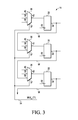
- FIG. 3 schematically shows an example of an embodiment of a scan chain.
- FIG. 4 schematically shows an example of an embodiment of a processing apparatus.
- FIG. 1 schematically illustrates a processing apparatus 10 .
- the processing apparatus 10 may comprise, for example, at least a first processing unit 12 and a second processing unit 14 , a set of synchronization data lines 34 , and a control unit 16 .
- the first processing unit 12 and the second processing unit 14 may, for example, be a first core and a second core, respectively.
- the first processing unit 12 may be arranged to be clocked by a first clock signal CLK_ 1 .
- the second processing unit 14 may be arranged to be clocked by a second clock signal CLK_ 2 .
- the first processing unit 12 may comprise a set of first stateful elements 18 .
- the second processing unit 14 may comprise a set of second stateful elements 20 .
- the set of synchronization data lines 34 may be operable to connect the first stateful elements 18 to the second stateful elements 20 in a pairwise manner.
- the control unit 16 may be operable to control the first processing unit 12 , the second processing unit 14 and the synchronization data lines 34 so as to copy the states of the first stateful elements 18 in parallel via the synchronization data lines 34 to the second stateful elements 20 in response to a synchronization request.
- Each of the synchronization data lines 34 may, for example, comprise a multiplexer 36 having an output 42 connected to an input 24 of one of the second stateful elements 20 , a normal data input 38 , and a synchronization data input 40 connected to one of the second stateful elements 20 .
- the respective multiplexer 36 may be integrated in the second processing unit 14 .
- the processing apparatus 10 comprises a first processing unit 12 and a second processing unit 14 .
- the processing apparatus 10 may comprise further processing units (not shown).
- the first processing unit 12 comprises a set of first stateful elements 18
- the second processing unit 14 comprises a set of second stateful elements 20 .
- the set of first stateful elements 18 comprises three stateful elements 18 .
- it may, of course, comprise a far greater number of stateful elements 18 , e.g. thousands or millions of such elements.
- the stateful elements 18 of the first processing unit 12 may be identical or different elements.
- some stateful elements 18 might be single bit elements while other stateful elements 18 might be multiple bit elements.
- the multiple bit elements may each have the same bit size or have different bit sizes.
- some or all of the first and second stateful elements 18 , 20 may be single bit elements.
- some or all of the first and second stateful elements 18 , 20 may be multiple bit elements.
- the stateful elements 18 are data flip-flops (DFF). Each stateful element 18 may have a data input 22 and a data output 26 . Each stateful element 18 may be set to a desired state by applying a suitable signal at data input 22 . The current state of each stateful element 18 may be read from the respective data output 26 . Each stateful element 18 may further comprise a clock input 30 .
- DFF data flip-flops
- the data inputs 22 and data outputs 26 of the stateful elements 18 may be suitably interconnected (not shown). For instance, data output 26 of the uppermost stateful element 18 in the figure may be connected to data input 22 of stateful element 18 in the center of the figure, while data output 26 of that latter stateful element 18 may in turn be connected to data input 22 of stateful element 18 near the bottom of the figure.
- the three shown stateful elements 18 may thus form, for example, a shift register.
- the data inputs 22 and data outputs 26 of the stateful elements 18 may alternatively be interconnected in any other suitable manner, directly or indirectly. They may, for example, be interconnected via logical circuitry not shown in the figure. For example, some or all of the stateful elements 18 may be interconnected to provide a digital signal processor, an arithmetic logic unit (ALU), or any other kind of structure.
- ALU arithmetic logic unit
- Each stateful element 20 may notably have a data input 24 and a data output 28 .
- Each stateful element 20 may further have a clock input 32 .
- Processing apparatus 10 may comprise further components not shown in the figure for the sake of simplicity and clarity.
- first processing unit 12 may be connected to a first memory, e.g. a first random access memory (RAM).
- second processing unit 14 may be connected to a second memory, e.g. a second random access memory. It is noted that synchronizing these memories may be a trivial task, as both processing units may, for instance, utilize a common memory comprising said first and second memories.
- First processing unit 12 and second processing unit 14 may be clocked by a first clock signal CLK_ 1 and a second clock signal CLK_ 2 , respectively.
- the first clock signal CLK_ 1 and the second clock signal CLK_ 2 may be the same, or they may differ.
- the clock rate of one of the two clock signals CLK_ 1 and CLK_ 2 may be reduced in order to save energy, while the other clock signal may have a normal clock rate.
- the processing apparatus 10 may be operated in a decoupled parallel mode (DPM) in which the first processing unit 12 and the second processing unit 14 may perform different tasks.
- DPM decoupled parallel mode
- the processing apparatus 10 may alternatively be operated in a redundant mode.
- the first processing unit 12 and the second processing unit 14 may independently execute the same instructions, starting from the same initial states and using the same input data.
- CLK_ 1 and CLK_ 2 are identical.
- a redundant mode in which the multiple processing units are clocked by the same clock signal is referred to as a lock-step mode (LSM).
- LSM lock-step mode
- the redundant mode is a lock-step mode, it must be ensured that the processing units have the same initial states at the same initial clock cycle. In other words, the processing units need to be synchronized prior to operating them in the lock-step mode.
- One option for passing from the decoupled parallel mode to a redundant mode can be to restart or to reset the processing apparatus 10 . This may be quite a lengthy procedure. Furthermore, it may involve the loss of current data.
- Another option may be copying by software. This also tends to be rather slow, as it may require millions of operations.
- a third option is to copy the present state of one of the processing units, referred to as a reference processing unit, to the other processing units, referred to as target processing units.
- the first processing unit 12 may serve as a reference processing unit, while the second processing unit 14 may serve as a target processing unit.
- the processing apparatus 10 may further comprise a set of synchronization data lines 34 .
- Each synchronization data line 34 may be operable to connect the data output 26 of one of the stateful elements 18 to the data input 24 of a corresponding stateful element 20 of the target processing unit 14 .
- the state of each stateful element 18 may thus be copied to the corresponding stateful element 20 via the respective synchronization data line 34 . More specifically, the states of the various stateful elements 18 may be copied in parallel, i.e., simultaneously, to the corresponding stateful element 20 .
- each synchronization data line 34 may comprise a multiplexer 36 .
- Each multiplexer 36 may have a normal data input 38 , a synchronization data input 40 , and a multiplexer output 42 .
- Each multiplexer output 42 may be connected to data input 24 of the respective stateful element 20 .
- Each normal data input 38 may be connected, directly or indirectly, to one of the data outputs 28 of the stateful elements 20 and/or to another node within the second processing unit 14 .
- the stateful elements 20 may be interconnected to form a logic that is analogous to the logic provided by the first stateful elements 18 of the first processing unit 12 .
- each synchronization data input 40 may be connected to data output 26 of the corresponding stateful element 18 of the first processing unit 12 .
- a multiplexer output 42 a given multiplexer 36 is connected to the synchronization data input 40 of that multiplexer 36 , the data output 26 of the corresponding stateful element 18 may thus be connected to the data input 24 of the corresponding second stateful element 20 .
- a synchronization connection between the respective first stateful element 18 and the corresponding second stateful element 20 may thus be established.
- Processing apparatus 10 may further comprise a control unit 16 .
- the control unit 16 may comprise a clock input 44 , a first clock output 48 , and a second clock output 46 .
- Control unit 16 may be operable to generate the above-mentioned first clock signal CLK_ 1 and second clock signal CLK_ 2 on the basis of an input clock signal CLK.
- control unit 16 may receive input clock signal CLK via clock input 44 and output the first and second clock signals CLK_ 1 and CLK_ 2 via the first and second clock outputs 48 and 46 , respectively.
- the first clock output 48 may be connected to clock inputs 30 of the first stateful elements 18 .
- the second clock output 46 may be connected to the clock inputs 32 of the second stateful elements 20 .
- the first clock signal CLK_ 1 and the second clock signal CLK_ 2 may thus be fed to the first processing unit 12 and to the second processing unit 14 , respectively.
- the processing apparatus 10 may comprise a multiplexer control bus 54 for feeding a multiplexer control signal MUX_CTL to each of the multiplexers 36 .
- Each of the multiplexers 36 may be arranged to connect its normal data input 38 to its multiplexer output 42 in response to the multiplexer control signal MUX_CTL indicating a normal operating mode, and to connect the synchronization data input 40 to the multiplexer output 42 in response to the multiplexer control signal MUX_CTL indicating a synchronization mode.
- the control unit 16 may be arranged to control the multiplexer control signal MUX_CTL to indicate the synchronization mode in response to the synchronization request, and to indicate the normal operating mode after completion of the copying.
- the normal operating mode may be a data processing mode of the processing apparatus, that is a mode in which the processing units process data, for example independently from each other.
- the normal operating mode may be established, for example, by connecting the stateful elements of each processing unit among each other in a suitable manner.
- a synchronization mode may be a mode in which one or more target processing units are being synchronized with respect to a reference processing unit.
- a synchronization mode is not a normal operating mode.
- a scan mode may be a test mode in which data may be extracted from one or more processing units via dedicated hardware, or in which data may be written to one or more processing units via the dedicated hardware.
- the dedicated hardware may, for example, comprise one or more scan chains.
- a scan mode is neither a normal operating mode nor a synchronization mode.
- control unit 16 may further comprise a mode input 50 and multiplexer control output 52 .
- Control unit 16 may be arranged to receive a mode signal via mode input 50 and to output a multiplexer control signal MUX_CTL at the multiplexer control output 52 .
- Multiplexer control output 52 may be connected to multiplexer control outputs 37 of the multiplexer 36 via a multiplexer control bus 54 .
- the mode signal MODE may, for example, indicate a normal operating mode.
- a normal operating mode is a mode in which the multiple processing units, e.g., processing unit 12 and processing unit 14 , operate normally to process data.
- the normal operating mode may, for example, be a decoupled parallel mode or a redundant mode.
- Control unit 16 in response to the mode signal MODE indicating the normal operating mode, may control, by means of multiplexer control signal MUX_CTL, the multiplexers 36 of the target processing unit so as to connect the multiplexer outputs 42 , and thus the data inputs 24 of the corresponding second stateful elements 20 , to the normal data inputs 38 .
- the data inputs 24 of the second stateful elements 20 may thus be connected to nodes within the second processing unit 14 .
- the mode signal MODE received at mode input 50 may alternatively indicate, for example, a synchronization mode.
- a synchronization mode is a mode in which states of a reference processing unit (in the example, the first processing unit 12 ) are copied to one or more target processing units (in the example, the second processing unit 14 ).
- the multiplexer control signal MUX_CTL may also be used as a status signal for indicating the current operating mode.
- the multiplexer control signal MUX_CTL may indicate the current operating mode to additional units (not shown) of the apparatus 10 or to other apparatuses (not shown).
- the control unit 16 may disable the first clock signal CLK_ 1 and the second clock signal CLK_ 2 in response to a synchronization request, and enable the first clock signal CLK_ 1 and the second clock signal CLK_ 2 after completion of the copying.
- Control unit 16 in response to the mode signal MODE indicating the synchronization mode, may control the multiplexers 36 , e.g. by means of multiplexer control signal MUX_CTL, so as to connect the multiplexer outputs 42 to the respective synchronization data inputs 40 .
- Control unit 16 may thus connect the data inputs 24 of the second stateful elements 20 to the corresponding data outputs 26 of the first stateful elements 18 .
- the control unit 16 may further issue one or more clock pulses to the second processing unit 14 so as to latch the states of the first stateful elements 18 into the second stateful elements 20 .
- the control unit 16 may notably issue the one or more clock pulses to the second processing unit 14 but not to the first processing unit 12 .
- processing apparatus 10 Operation of processing apparatus 10 is further explained with additional reference to FIG. 2 .
- a requesting unit for example, the reference processing unit 12 or the target processing unit 14 or some external unit, may issue a request indicating that the processing apparatus 10 should enter a redundant mode, for example, a lock-step mode (block S 1 ).
- the processing apparatus 10 in response to the request for entering the redundant mode and upon determining that the processing apparatus 10 is currently not in the redundant mode, may issue a request that the processing units of the processing apparatus (processing units 12 and 14 in the example) be synchronized (block S 2 ).
- Processing apparatus 10 may accordingly set the mode signal MODE (see FIG. 1 ) to indicate the synchronization mode.
- the control unit 16 in response to the mode signal MODE newly indicating the synchronization mode, may disable the first clock signal CLK_ 1 and the second clock signal CLK_ 2 (block S 3 ).
- the states of the first processing unit 12 and of the second processing unit 14 may thus be “frozen”. Their content, and notably the content of the reference processing unit 12 , is thus preserved.
- the control unit 16 may then proceed to establish the pairwise synchronization data connections from data outputs 26 of stateful elements 18 of the reference processing unit 12 to data inputs 24 of stateful elements 20 of the target processing unit 14 .
- the pairwise synchronization data connections are established by controlling multiplexers 36 so as to connect the respective synchronization data inputs 40 to the multiplexer outputs 42 (block S 4 ).
- the control unit 16 after establishing the synchronization data connections may wait during a short interval, e.g., a predefined interval, to allow the state information that is output at the data outputs 26 of the first stateful elements 18 , to propagate from the data outputs 26 to the corresponding data inputs 24 of the second stateful elements 20 (block S 5 ).
- a short interval e.g., a predefined interval
- the control unit 16 may then issue one or more clock pulses at least to the target processing unit 14 , e.g. by controlling the second clock signal CLK_ 2 accordingly (block S 6 ).
- the state information applied at data inputs 24 of the second stateful elements 20 may thus be latched into the second stateful elements 20 .
- the number of clock pulses that is sufficient for latching the entire state of a first stateful element 18 to a corresponding second stateful element 20 may depend, firstly, on the bit size of a state and, secondly, on the number of bits that can be transferred per clock cycle via the respective synchronization data line 34 .
- first stateful element 18 and the corresponding second stateful element 20 may each be a register of bit size N, and synchronization data line 34 may be a multiple data line capable of transferring a total of N bits simultaneously, N being a natural number. A single clock pulse will be sufficient for such a layout.
- First stateful element 18 and second stateful element 20 may notably each be a data flip-flop that is a stateful element of bit size 1 , while synchronization data line may be a simple (that is, not multiple) data line.
- the control unit 16 may then re-establish the normal data connections (block S 7 ).
- the normal data connection may be established by controlling the multiplexers 36 so as to connect the normal data inputs 38 to the respective multiplexer outputs 42 .
- the control unit 16 may re-enable the clock signals CLK_ 1 and CLK_ 2 to the reference processing unit 12 and the target processing unit 14 , respectively (block S 8 ). If the requested redundant mode is a lock-step mode, the control unit 16 may generate the first clock signal CLK_ 1 and the second clock signal CLK_ 2 such that the clock rates are identical. The control unit 16 may, for example, feed the same clock signal to reference processing unit 12 and to the target processing unit 14 (in this case CLK_ 1 and CLK_ 2 may be equal). The transition from the decoupled parallel mode to the redundant mode may thus be complete.
- a first processing unit 12 and a second processing unit 14 of a processing apparatus 10 may be synchronized by connecting the first stateful elements 18 to the second stateful elements 20 in a pairwise manner and copying the states of the first stateful elements 18 in parallel to the second stateful elements 20 .
- the technique may notably comprise: clocking the first processing unit 12 and the second processing unit 14 by a first clock signal CLK_ 1 and a second clock signal CLK_ 2 , respectively; disabling the first clock signal CLK_ 1 and the second clock signal CLK_ 2 prior to the connecting; issuing a clock pulse to the second stateful elements 20 ; and enabling the first clock signal CLK_ 1 and the second clock signal CLK_ 2 .
- the processing apparatus 10 may comprise a scan chain 58 , 20 .
- the scan chain may comprise at least some of the second stateful elements 20 .
- the scan chain may further comprise at least some of the multiplexers 36 .
- Each of the multiplexers 36 of the scan chain except possibly a first one of these multiplexers 36 , may have a scan data input 56 connected to an output 28 of a preceding stateful element 20 of the scan chain 58 .
- the first member of the scan chain does not necessarily have a preceding member; therefore the first one of these multiplexers may be arranged differently.
- the scan chain may be arranged as a daisy chain, for example.
- the scan chain 58 may be part of a design-for-test (DFT) circuitry.
- the DFT circuitry may, for example, be operated using a JTAG protocol.
- the DFT circuitry may be adapted for parallel data transfer from the first processing unit 12 to the second processing unit 14 .
- the target processing unit 14 described above in reference to FIGS. 1 and 2 may comprise a scan chain for extracting data from or writing data to the stateful elements 20 .
- the scan chain may be implemented in a particularly convenient manner by adapting the multiplexers 36 described above in reference to FIGS. 1 and 2 .
- each multiplexer 36 may comprise a scan data input 56 .
- Each scan data input 56 may be connected via a scan data line 58 to the data output 28 of one of the other stateful elements 20 .
- the control unit 16 described above in reference to FIGS. 1 and 2 may, in response to the mode signal MODE indicating a scan mode, control the multiplexers 36 so as to connect the scan data inputs 56 to the respective multiplexer outputs 42 .
- the scan chain may thus be established.
- Each segment of the scan chain may thus comprise, in this order, a multiplexer 36 , a subsequent stateful element 20 , and a subsequent scan data line 58 .
- a different layout may be adopted notably for the first and/or last segment of the scan chain.
- FIG. 4 schematically represents an example of another processing apparatus 10 as described above in reference to FIGS. 1, 2, and 3 .
- the processing apparatus 10 may comprise a set of reverse synchronization data lines 60 .
- the reverse synchronization data lines 60 may be operable to connect the second stateful elements 20 to the first stateful elements 18 in a pairwise manner.
- the control unit 16 may be operable to control the first processing unit 12 , the second processing unit 14 and the reverse synchronization data lines 60 so as to copy the states of the second stateful elements 20 in parallel via the reverse synchronization data lines 60 to the first stateful elements 18 in response to a reverse synchronization request.
- the shown apparatus 10 may, for example, have a layout that is symmetrical in regard to the first processing unit 12 and the second processing unit 14 .
- Each processing unit may, of course, comprise a large number of stateful elements as schematically illustrated in FIGS. 1 and 3 .
- the first processing unit 12 may notably comprise a scan chain comprising the first stateful elements 18 .
- the second processing unit 14 may comprise a second scan chain comprising the second stateful elements 20 .
- the first scan chain and the second scan chain may be arranged as described above by way of example in reference to FIG. 3 .
- the first scan chain and the second scan chain may also be arranged as described in the above-mentioned international publication WO 2009/138819 A1 (Bogenberger et al.). Both the first scan chain and the second scan chain may notably form a daisy chain.
- the first processing unit 12 may notably comprise a set of reverse synchronization data lines 60 and a set of multiplexers 62 .
- Reverse synchronization data lines 60 may connect data outputs 28 to synchronization data inputs 66 in a pairwise manner.
- Reverse synchronization data line 60 may thus be analogous to (forward) synchronization data lines 34 .
- Each multiplexer 62 may have a normal data input 64 , a synchronization data input 66 , a scan data input 68 , a multiplexer output 70 , and a multiplexer control input 63 .
- Multiplexer output 70 may be connected to data input 22 .
- Multiplexer control bus 54 may connect multiplexer control output 52 to both multiplexer control input 37 and multiplexer control input 63 .
- Processing apparatus 10 may thus be operated to synchronize second processing unit 14 with first processing unit 12 as described above in reference to FIGS. 1, 2, and 3 (forward synchronization) and, alternatively, to synchronize first processing unit 12 with second processing unit 14 (reverse synchronization).
- Processing apparatus 10 may further be operable to swap the states of first processing unit 12 and second processing unit 14 .
- a flexible solution which may allow a processing apparatus to switch dynamically from an asynchronous to a synchronous mode of operation, and vice versa.
- No initialization and/or wait time may be required, as the processing units may be synchronized as fast as in only a few clock cycles. Depending on the design, synchronization in only one clock cycle may be possible.
- a device reset may not be necessary.
- Known scan chain arrangements may be adapted, thus avoiding or minimizing the need for additional dedicated components.
- the device availability time may be significantly increased while safety features may remain intact. It may possible to resolve peak processing loads more rapidly and more easily by switching from a lock step mode to a decoupled parallel mode.
- the design also lends itself to the introduction of further self-test features, such as error injection.
- a computer program is a list of instructions such as a particular application program and/or an operating system.
- the computer program may for instance include one or more of: a subroutine, a function, a procedure, an object method, an object implementation, an executable application, an applet, a servlet, a source code, an object code, a shared library/dynamic load library and/or other sequence of instructions designed for execution on a computer system.
- the computer program may be stored internally on computer readable storage medium or transmitted to the computer system via a computer readable transmission medium. All or some of the computer program may be provided on computer readable media permanently, removably or remotely coupled to an information processing system.
- the computer readable media may include, for example and without limitation, any number of the following: magnetic storage media including disk and tape storage media; optical storage media such as compact disk media (e.g., CD-ROM, CD-R, etc.) and digital video disk storage media; nonvolatile memory storage media including semiconductor-based memory units such as FLASH memory, EEPROM, EPROM, ROM; ferromagnetic digital memories; MRAM; volatile storage media including registers, buffers or caches, main memory, RAM, etc.; and data transmission media including computer networks, point-to-point telecommunication equipment, and carrier wave transmission media, just to name a few.
- a computer process typically includes an executing (running) program or portion of a program, current program values and state information, and the resources used by the operating system to manage the execution of the process.
- An operating system is the software that manages the sharing of the resources of a computer and provides programmers with an interface used to access those resources.
- An operating system processes system data and user input, and responds by allocating and managing tasks and internal system resources as a service to users and programs of the system.
- the computer system may for instance include at least one processing unit, associated memory and a number of input/output (I/O) devices.
- I/O input/output
- the computer system processes information according to the computer program and produces resultant output information via I/O devices.
- two nodes are said to be connected if data may be propagate from one of the nodes to the other node.
- charge transfer electrical current
- two nodes are said to be connected if charge may propagate from one of the nodes to the other node.
- connections as discussed herein may be any type of connection suitable to transfer signals from or to the respective nodes, units or devices, for example via intermediate devices. Accordingly, unless implied or stated otherwise, the connections may for example be direct connections or indirect connections.
- the connections may be illustrated or described in reference to being a single connection, a plurality of connections, unidirectional connections, or bidirectional connections. However, different embodiments may vary the implementation of the connections. For example, separate unidirectional connections may be used rather than bidirectional connections and vice versa.
- plurality of connections may be replaced with a single connections that transfers multiple signals serially or in a time multiplexed manner. Likewise, single connections carrying multiple signals may be separated out into various different connections carrying subsets of these signals. Therefore, many options exist for transferring signals.
- Each signal described herein may be designed as positive or negative logic.
- the signal In the case of a negative logic signal, the signal is active low where the logically true state corresponds to a logic level zero.
- the signal In the case of a positive logic signal, the signal is active high where the logically true state corresponds to a logic level one.
- any of the signals described herein can be designed as either negative or positive logic signals. Therefore, in alternate embodiments, those signals described as positive logic signals may be implemented as negative logic signals, and those signals described as negative logic signals may be implemented as positive logic signals.
- assert or “set” and “negate” (or “deassert” or “clear”) are used herein when referring to the rendering of a signal, status bit, or similar apparatus into its logically true or logically false state, respectively. If the logically true state is a logic level one, the logically false state is a logic level zero. And if the logically true state is a logic level zero, the logically false state is a logic level one.
- logic blocks are merely illustrative and that alternative embodiments may merge logic blocks or circuit elements or impose an alternate decomposition of functionality upon various logic blocks or circuit elements.
- the architectures depicted herein are merely exemplary, and that in fact many other architectures can be implemented which achieve the same functionality. For example, two or more first stateful elements 18 may be combined in one stateful element. Similarly, two or more second stateful elements 20 may be combined in one stateful element.
- any arrangement of components to achieve the same functionality is effectively “associated” such that the desired functionality is achieved.
- any two components herein combined to achieve a particular functionality can be seen as “associated with” each other such that the desired functionality is achieved, irrespective of architectures or intermedial components.
- any two components so associated can also be viewed as being “operably connected,” or “operably coupled,” to each other to achieve the desired functionality.
- the illustrated examples may be implemented as circuitry located on a single integrated circuit or within a same device.
- processing units 12 and 14 and control unit 16 may be located on a single integrated circuit or within a same device.
- the examples may be implemented as any number of separate integrated circuits or separate devices interconnected with each other in a suitable manner.
- processing units 12 and 14 and control unit 16 may be implemented as three separate integrated circuits or separate devices interconnected with each other in a suitable manner.
- the examples, or portions thereof may implemented as soft or code representations of physical circuitry or of logical representations convertible into physical circuitry, such as in a hardware description language of any appropriate type.
- the invention is not limited to physical devices or units implemented in non-programmable hardware but can also be applied in programmable devices or units able to perform the desired device functions by operating in accordance with suitable program code, such as mainframes, minicomputers, servers, workstations, personal computers, notepads, personal digital assistants, electronic games, automotive and other embedded systems, cell phones and various other wireless devices, commonly denoted in this application as ‘computer systems’.
- suitable program code such as mainframes, minicomputers, servers, workstations, personal computers, notepads, personal digital assistants, electronic games, automotive and other embedded systems, cell phones and various other wireless devices, commonly denoted in this application as ‘computer systems’.
- any reference signs placed between parentheses shall not be construed as limiting the claim.
- the word ‘comprising’ does not exclude the presence of other elements or steps then those listed in a claim.
- the terms “a” or “an,” as used herein, are defined as one or more than one.
Landscapes
- Engineering & Computer Science (AREA)
- Theoretical Computer Science (AREA)
- Physics & Mathematics (AREA)
- General Engineering & Computer Science (AREA)
- General Physics & Mathematics (AREA)
- Software Systems (AREA)
- Quality & Reliability (AREA)
- Electronic Switches (AREA)
- Logic Circuits (AREA)
- Semiconductor Integrated Circuits (AREA)
Abstract
Description
Claims (20)
Applications Claiming Priority (1)
| Application Number | Priority Date | Filing Date | Title |
|---|---|---|---|
| PCT/IB2011/053232 WO2013011353A1 (en) | 2011-07-20 | 2011-07-20 | Processing apparatus and method of synchronizing a first processing unit and a second processing unit |
Publications (2)
| Publication Number | Publication Date |
|---|---|
| US20140173247A1 US20140173247A1 (en) | 2014-06-19 |
| US9665377B2 true US9665377B2 (en) | 2017-05-30 |
Family
ID=47557714
Family Applications (1)
| Application Number | Title | Priority Date | Filing Date |
|---|---|---|---|
| US14/125,200 Active 2033-02-18 US9665377B2 (en) | 2011-07-20 | 2011-07-20 | Processing apparatus and method of synchronizing a first processing unit and a second processing unit |
Country Status (3)
| Country | Link |
|---|---|
| US (1) | US9665377B2 (en) |
| CN (1) | CN103703427B (en) |
| WO (1) | WO2013011353A1 (en) |
Families Citing this family (6)
| Publication number | Priority date | Publication date | Assignee | Title |
|---|---|---|---|---|
| US20150178102A1 (en) * | 2011-11-23 | 2015-06-25 | Freescale Semiconductor, Inc. | System-on-chip, method of manufacture thereof and method of controlling a system-on-chip |
| US9614740B2 (en) * | 2014-05-13 | 2017-04-04 | International Business Machines Corporation | Multifusion of a stream operator in a streaming application |
| DE102014213245A1 (en) | 2014-07-08 | 2016-01-14 | Robert Bosch Gmbh | Method for processing data for a driving function of a vehicle |
| WO2018128204A1 (en) * | 2017-01-06 | 2018-07-12 | 주식회사 알티스트 | Multicore system capable of using lsm and dpm simultaneously by using partitioning technique |
| US10429919B2 (en) | 2017-06-28 | 2019-10-01 | Intel Corporation | System, apparatus and method for loose lock-step redundancy power management |
| TWI729825B (en) * | 2020-05-26 | 2021-06-01 | 友達光電股份有限公司 | Driving circuit and shift register |
Citations (17)
| Publication number | Priority date | Publication date | Assignee | Title |
|---|---|---|---|---|
| US4358823A (en) * | 1977-03-25 | 1982-11-09 | Trw, Inc. | Double redundant processor |
| EP0372580A2 (en) | 1987-11-09 | 1990-06-13 | Tandem Computers Incorporated | Synchronization of fault-tolerant computer system having multiple processors |
| US5758058A (en) | 1993-03-31 | 1998-05-26 | Intel Corporation | Apparatus and method for initializing a master/checker fault detecting microprocessor |
| US5838894A (en) * | 1992-12-17 | 1998-11-17 | Tandem Computers Incorporated | Logical, fail-functional, dual central processor units formed from three processor units |
| US6311289B1 (en) * | 1998-11-03 | 2001-10-30 | Telefonaktiebolaget Lm Ericsson (Publ) | Explicit state copy in a fault tolerant system using a remote write operation |
| US6694449B2 (en) * | 1998-07-16 | 2004-02-17 | Siemens Aktiengesellschaft | Duplicable processor device |
| US20040093435A1 (en) | 2001-03-29 | 2004-05-13 | Juha Purho | Method for synchronizing a first clock to a second clock, processing unit and synchronization system |
| US20050034017A1 (en) | 2003-08-04 | 2005-02-10 | Cedric Airaud | Cross-triggering of processing devices |
| US7085959B2 (en) * | 2002-07-03 | 2006-08-01 | Hewlett-Packard Development Company, L.P. | Method and apparatus for recovery from loss of lock step |
| US20070174687A1 (en) | 2006-01-10 | 2007-07-26 | Stratus Technologies Bermuda Ltd. | Systems and methods for maintaining lock step operation |
| US7328371B1 (en) * | 2004-10-15 | 2008-02-05 | Advanced Micro Devices, Inc. | Core redundancy in a chip multiprocessor for highly reliable systems |
| CN101251816A (en) | 2008-03-13 | 2008-08-27 | 中国科学院计算技术研究所 | Redundant system for programmable device and redundant implementing method |
| US7519856B2 (en) | 2004-12-21 | 2009-04-14 | Nec Corporation | Fault tolerant system and controller, operation method, and operation program used in the fault tolerant system |
| WO2009138819A1 (en) | 2008-05-14 | 2009-11-19 | Freescale Semiconductor, Inc. | Processing resource apparatus and method of synchronising a processing resource |
| US7859542B1 (en) | 2003-04-17 | 2010-12-28 | Nvidia Corporation | Method for synchronizing graphics processing units |
| US20110148890A1 (en) | 2009-12-23 | 2011-06-23 | Nikos Kaburlasos | Synchronized media processing |
| US20120030504A1 (en) | 2009-03-19 | 2012-02-02 | Hitachi, Ltd. | High reliability computer system and its configuration method |
-
2011
- 2011-07-20 WO PCT/IB2011/053232 patent/WO2013011353A1/en active Application Filing
- 2011-07-20 CN CN201180072400.8A patent/CN103703427B/en active Active
- 2011-07-20 US US14/125,200 patent/US9665377B2/en active Active
Patent Citations (18)
| Publication number | Priority date | Publication date | Assignee | Title |
|---|---|---|---|---|
| US4358823A (en) * | 1977-03-25 | 1982-11-09 | Trw, Inc. | Double redundant processor |
| EP0372580A2 (en) | 1987-11-09 | 1990-06-13 | Tandem Computers Incorporated | Synchronization of fault-tolerant computer system having multiple processors |
| US5838894A (en) * | 1992-12-17 | 1998-11-17 | Tandem Computers Incorporated | Logical, fail-functional, dual central processor units formed from three processor units |
| US5758058A (en) | 1993-03-31 | 1998-05-26 | Intel Corporation | Apparatus and method for initializing a master/checker fault detecting microprocessor |
| US6694449B2 (en) * | 1998-07-16 | 2004-02-17 | Siemens Aktiengesellschaft | Duplicable processor device |
| US6311289B1 (en) * | 1998-11-03 | 2001-10-30 | Telefonaktiebolaget Lm Ericsson (Publ) | Explicit state copy in a fault tolerant system using a remote write operation |
| US20040093435A1 (en) | 2001-03-29 | 2004-05-13 | Juha Purho | Method for synchronizing a first clock to a second clock, processing unit and synchronization system |
| US7085959B2 (en) * | 2002-07-03 | 2006-08-01 | Hewlett-Packard Development Company, L.P. | Method and apparatus for recovery from loss of lock step |
| US7859542B1 (en) | 2003-04-17 | 2010-12-28 | Nvidia Corporation | Method for synchronizing graphics processing units |
| US20050034017A1 (en) | 2003-08-04 | 2005-02-10 | Cedric Airaud | Cross-triggering of processing devices |
| US7328371B1 (en) * | 2004-10-15 | 2008-02-05 | Advanced Micro Devices, Inc. | Core redundancy in a chip multiprocessor for highly reliable systems |
| US7519856B2 (en) | 2004-12-21 | 2009-04-14 | Nec Corporation | Fault tolerant system and controller, operation method, and operation program used in the fault tolerant system |
| US20070174687A1 (en) | 2006-01-10 | 2007-07-26 | Stratus Technologies Bermuda Ltd. | Systems and methods for maintaining lock step operation |
| CN101251816A (en) | 2008-03-13 | 2008-08-27 | 中国科学院计算技术研究所 | Redundant system for programmable device and redundant implementing method |
| WO2009138819A1 (en) | 2008-05-14 | 2009-11-19 | Freescale Semiconductor, Inc. | Processing resource apparatus and method of synchronising a processing resource |
| US20110035750A1 (en) | 2008-05-14 | 2011-02-10 | Freescale Semiconductor, Inc. | Processing resource apparatus and method of synchronising a processing resource |
| US20120030504A1 (en) | 2009-03-19 | 2012-02-02 | Hitachi, Ltd. | High reliability computer system and its configuration method |
| US20110148890A1 (en) | 2009-12-23 | 2011-06-23 | Nikos Kaburlasos | Synchronized media processing |
Non-Patent Citations (1)
| Title |
|---|
| International Search Report and Written Opinion correlating to PCT/IB2011/053232 dated Mar. 13, 2012. |
Also Published As
| Publication number | Publication date |
|---|---|
| CN103703427B (en) | 2016-05-11 |
| CN103703427A (en) | 2014-04-02 |
| US20140173247A1 (en) | 2014-06-19 |
| WO2013011353A1 (en) | 2013-01-24 |
Similar Documents
| Publication | Publication Date | Title |
|---|---|---|
| US10942737B2 (en) | Method, device and system for control signalling in a data path module of a data stream processing engine | |
| US9665377B2 (en) | Processing apparatus and method of synchronizing a first processing unit and a second processing unit | |
| US9823983B2 (en) | Electronic fault detection unit | |
| CN107045479B (en) | High performance interconnect physical layer | |
| US9405552B2 (en) | Method, device and system for controlling execution of an instruction sequence in a data stream accelerator | |
| US9286067B2 (en) | Method and apparatus for a hierarchical synchronization barrier in a multi-node system | |
| JP5826865B2 (en) | Integrated circuit with programmable circuit and embedded processor system | |
| US9141178B2 (en) | Device and method for selective reduced power mode in volatile memory units | |
| US10184983B2 (en) | Interface independent test boot method and apparatus using automatic test equipment | |
| US20130227257A1 (en) | Data processor with asynchronous reset | |
| US8977835B2 (en) | Reversing processing order in half-pumped SIMD execution units to achieve K cycle issue-to-issue latency | |
| US20140325183A1 (en) | Integrated circuit device, asymmetric multi-core processing module, electronic device and method of managing execution of computer program code therefor | |
| US8631292B2 (en) | Multi-threading flip-flop circuit | |
| US10996267B2 (en) | Time interleaved scan system | |
| US9000804B2 (en) | Integrated circuit device comprising clock gating circuitry, electronic device and method for dynamically configuring clock gating | |
| JP7416429B2 (en) | Flexible logic unit suitable for real-time task switching | |
| US11455261B2 (en) | First boot with one memory channel | |
| US20220043475A1 (en) | Access to multiple timing domains | |
| US20140115358A1 (en) | Integrated circuit device and method for controlling an operating mode of an on-die memory | |
| US6944784B2 (en) | Flip-flop having multiple clock sources and method therefore | |
| US9116701B2 (en) | Memory unit, information processing device, and method | |
| US9678808B2 (en) | Method and apparatus for write-only inter-processor reset synchronization | |
| US12117878B2 (en) | Methods and apparatus to reduce display connection latency | |
| US11706150B2 (en) | Data encoding and packet sharing in a parallel communication interface | |
| US20140365748A1 (en) | Method, apparatus and system for data stream processing with a programmable accelerator |
Legal Events
| Date | Code | Title | Description |
|---|---|---|---|
| AS | Assignment |
Owner name: FREESCALE SEMICONDUCTOR INC., TEXAS Free format text: ASSIGNMENT OF ASSIGNORS INTEREST;ASSIGNORS:LITOVTCHENKO, VLADIMIR;LUEPKEN, HARALD;REGNER, MARKUS;REEL/FRAME:031751/0490 Effective date: 20110914 |
|
| AS | Assignment |
Owner name: CITIBANK, N.A., AS NOTES COLLATERAL AGENT, NEW YOR Free format text: SUPPLEMENT TO IP SECURITY AGREEMENT;ASSIGNOR:FREESCALE SEMICONDUCTOR, INC.;REEL/FRAME:032445/0577 Effective date: 20140217 Owner name: CITIBANK, N.A., COLLATERAL AGENT, NEW YORK Free format text: SUPPLEMENT TO IP SECURITY AGREEMENT;ASSIGNOR:FREESCALE SEMICONDUCTOR, INC.;REEL/FRAME:032445/0689 Effective date: 20140217 Owner name: CITIBANK, N.A., AS NOTES COLLATERAL AGENT, NEW YOR Free format text: SUPPLEMENT TO IP SECURITY AGREEMENT;ASSIGNOR:FREESCALE SEMICONDUCTOR, INC.;REEL/FRAME:032445/0493 Effective date: 20140217 |
|
| AS | Assignment |
Owner name: FREESCALE SEMICONDUCTOR, INC., TEXAS Free format text: PATENT RELEASE;ASSIGNOR:CITIBANK, N.A., AS COLLATERAL AGENT;REEL/FRAME:037357/0790 Effective date: 20151207 |
|
| AS | Assignment |
Owner name: MORGAN STANLEY SENIOR FOUNDING, INC., MARYLAND Free format text: ASSIGNMENT AND ASSUMPTION OF SECURITY INTEREST IN PATENTS;ASSIGNOR:CITIBANK, N.A.;REEL/FRAME:037458/0399 Effective date: 20151207 Owner name: MORGAN STANLEY SENIOR FOUNDING, INC., MARYLAND Free format text: ASSIGNMENT AND ASSUMPTION OF SECURITY INTEREST IN PATENTS;ASSIGNOR:CITIBANK, N.A.;REEL/FRAME:037458/0420 Effective date: 20151207 |
|
| AS | Assignment |
Owner name: MORGAN STANLEY SENIOR FUNDING, INC., MARYLAND Free format text: CORRECTIVE ASSIGNMENT TO CORRECT THE ASSIGNEE NAME PREVIOUSLY RECORDED ON REEL 037458 FRAME 0399. ASSIGNOR(S) HEREBY CONFIRMS THE ASSIGNMENT AND ASSUMPTION OF SECURITY INTEREST IN PATENTS;ASSIGNOR:CITIBANK, N.A.;REEL/FRAME:037515/0390 Effective date: 20151207 Owner name: MORGAN STANLEY SENIOR FUNDING, INC., MARYLAND Free format text: CORRECTIVE ASSIGNMENT TO CORRECT THE ASSIGNEE NAME PREVIOUSLY RECORDED ON REEL 037458 FRAME 0420. ASSIGNOR(S) HEREBY CONFIRMS THE ASSIGNMENT AND ASSUMPTION OF SECURITY INTEREST IN PATENTS;ASSIGNOR:CITIBANK, N.A.;REEL/FRAME:037515/0420 Effective date: 20151207 |
|
| AS | Assignment |
Owner name: MORGAN STANLEY SENIOR FUNDING, INC., MARYLAND Free format text: CORRECTIVE ASSIGNMENT TO REMOVE PATENT APPLICATION NUMBER 14085520 REPLACE IT WITH 14086520 PREVIOUSLY RECORDED AT REEL: 037458 FRAME: 0399. ASSIGNOR(S) HEREBY CONFIRMS THE ASSIGNMENT AND ASSUMPTION OF SECURITY INTEREST IN PATENTS;ASSIGNOR:CITIBANK, N.A.;REEL/FRAME:037785/0454 Effective date: 20151207 Owner name: MORGAN STANLEY SENIOR FUNDING, INC., MARYLAND Free format text: CORRECTIVE ASSIGNMENT TO REMOVE NUMBER 14085520 SHOULD BE 14086520 PREVIOUSLY RECORDED AT REEL: 037458 FRAME: 0420. ASSIGNOR(S) HEREBY CONFIRMS THE ASSIGNMENT AND ASSUMPTON OF SECURITY INTEREST IN PATENTS;ASSIGNOR:CITIBANK, N.A.;REEL/FRAME:037785/0568 Effective date: 20151207 Owner name: MORGAN STANLEY SENIOR FUNDING, INC., MARYLAND Free format text: CORRECTIVE ASSIGNMENT TO REMOVE APPL. NO. 14/085,520 AND REPLACE 14/086,520 PREVIOUSLY RECORDED AT REEL: 037515 FRAME: 0390. ASSIGNOR(S) HEREBY CONFIRMS THE ASSIGNMENT AND ASSUMPTION OF SECURITY INTEREST IN PATENTS;ASSIGNOR:CITIBANK, N.A.;REEL/FRAME:037792/0227 Effective date: 20151207 Owner name: MORGAN STANLEY SENIOR FUNDING, INC., MARYLAND Free format text: CORRECTIVE ASSIGNMENT OF INCORRECT APPL. NO. 14/085,520 PREVIOUSLY RECORDED AT REEL: 037515 FRAME: 0390. ASSIGNOR(S) HEREBY CONFIRMS THE ASSIGNMENT AND ASSUMPTION OF SECURITY INTEREST IN PATENTS;ASSIGNOR:CITIBANK, N.A.;REEL/FRAME:037792/0227 Effective date: 20151207 Owner name: MORGAN STANLEY SENIOR FUNDING, INC., MARYLAND Free format text: CORRECTIVE ASSIGNMENT TO CORRECT THE INCORRECT APPL. NO. 14/085,520 PREVIOUSLY RECORDED AT REEL: 037515 FRAME: 0420. ASSIGNOR(S) HEREBY CONFIRMS THE ASSIGNMENT AND ASSUMPTION OF SECURITY INTEREST IN PATENTS;ASSIGNOR:CITIBANK, N.A.;REEL/FRAME:037879/0581 Effective date: 20151207 Owner name: MORGAN STANLEY SENIOR FUNDING, INC., MARYLAND Free format text: CORRECTIVE ASSIGNMENT OF INCORRECT PATENT APPLICATION NUMBER 14085520 ,PREVIOUSLY RECORDED AT REEL: 037458 FRAME: 0399. ASSIGNOR(S) HEREBY CONFIRMS THE ASSIGNMENT AND ASSUMPTION OF SECURITY INTEREST IN PATENTS;ASSIGNOR:CITIBANK, N.A.;REEL/FRAME:037785/0454 Effective date: 20151207 Owner name: MORGAN STANLEY SENIOR FUNDING, INC., MARYLAND Free format text: CORRECTIVE ASSIGNMENT OF INCORRECT NUMBER 14085520 PREVIOUSLY RECORDED AT REEL: 037458 FRAME: 0420. ASSIGNOR(S) HEREBY CONFIRMS THE ASSIGNMENT AND ASSUMPTON OF SECURITY INTEREST IN PATENTS;ASSIGNOR:CITIBANK, N.A.;REEL/FRAME:037785/0568 Effective date: 20151207 |
|
| AS | Assignment |
Owner name: MORGAN STANLEY SENIOR FUNDING, INC., MARYLAND Free format text: CORRECTIVE ASSIGNMENT TO CORRECT THE FILING AND REMOVE APPL. NO. 14085520 REPLACE IT WITH 14086520 PREVIOUSLY RECORDED AT REEL: 037515 FRAME: 0390. ASSIGNOR(S) HEREBY CONFIRMS THE ASSIGNMENT AND ASSUMPTION OF SECURITY INTEREST IN PATENTS;ASSIGNOR:CITIBANK, N.A.;REEL/FRAME:037926/0642 Effective date: 20151207 |
|
| AS | Assignment |
Owner name: MORGAN STANLEY SENIOR FUNDING, INC., MARYLAND Free format text: SECURITY AGREEMENT SUPPLEMENT;ASSIGNOR:NXP B.V.;REEL/FRAME:038017/0058 Effective date: 20160218 |
|
| AS | Assignment |
Owner name: MORGAN STANLEY SENIOR FUNDING, INC., MARYLAND Free format text: SUPPLEMENT TO THE SECURITY AGREEMENT;ASSIGNOR:FREESCALE SEMICONDUCTOR, INC.;REEL/FRAME:039138/0001 Effective date: 20160525 |
|
| AS | Assignment |
Owner name: MORGAN STANLEY SENIOR FUNDING, INC., MARYLAND Free format text: CORRECTIVE ASSIGNMENT TO CORRECT THE REMOVE APPLICATION 12092129 PREVIOUSLY RECORDED ON REEL 038017 FRAME 0058. ASSIGNOR(S) HEREBY CONFIRMS THE SECURITY AGREEMENT SUPPLEMENT;ASSIGNOR:NXP B.V.;REEL/FRAME:039361/0212 Effective date: 20160218 |
|
| AS | Assignment |
Owner name: NXP, B.V., F/K/A FREESCALE SEMICONDUCTOR, INC., NETHERLANDS Free format text: RELEASE BY SECURED PARTY;ASSIGNOR:MORGAN STANLEY SENIOR FUNDING, INC.;REEL/FRAME:040925/0001 Effective date: 20160912 Owner name: NXP, B.V., F/K/A FREESCALE SEMICONDUCTOR, INC., NE Free format text: RELEASE BY SECURED PARTY;ASSIGNOR:MORGAN STANLEY SENIOR FUNDING, INC.;REEL/FRAME:040925/0001 Effective date: 20160912 |
|
| AS | Assignment |
Owner name: NXP B.V., NETHERLANDS Free format text: RELEASE BY SECURED PARTY;ASSIGNOR:MORGAN STANLEY SENIOR FUNDING, INC.;REEL/FRAME:040928/0001 Effective date: 20160622 |
|
| AS | Assignment |
Owner name: NXP USA, INC., TEXAS Free format text: CHANGE OF NAME;ASSIGNOR:FREESCALE SEMICONDUCTOR INC.;REEL/FRAME:040626/0683 Effective date: 20161107 |
|
| AS | Assignment |
Owner name: NXP USA, INC., TEXAS Free format text: CORRECTIVE ASSIGNMENT TO CORRECT THE NATURE OF CONVEYANCE PREVIOUSLY RECORDED AT REEL: 040626 FRAME: 0683. ASSIGNOR(S) HEREBY CONFIRMS THE MERGER AND CHANGE OF NAME;ASSIGNOR:FREESCALE SEMICONDUCTOR INC.;REEL/FRAME:041414/0883 Effective date: 20161107 Owner name: NXP USA, INC., TEXAS Free format text: CORRECTIVE ASSIGNMENT TO CORRECT THE NATURE OF CONVEYANCE PREVIOUSLY RECORDED AT REEL: 040626 FRAME: 0683. ASSIGNOR(S) HEREBY CONFIRMS THE MERGER AND CHANGE OF NAME EFFECTIVE NOVEMBER 7, 2016;ASSIGNORS:NXP SEMICONDUCTORS USA, INC. (MERGED INTO);FREESCALE SEMICONDUCTOR, INC. (UNDER);SIGNING DATES FROM 20161104 TO 20161107;REEL/FRAME:041414/0883 |
|
| AS | Assignment |
Owner name: MORGAN STANLEY SENIOR FUNDING, INC., MARYLAND Free format text: CORRECTIVE ASSIGNMENT TO CORRECT THE REMOVE APPLICATION 12681366 PREVIOUSLY RECORDED ON REEL 039361 FRAME 0212. ASSIGNOR(S) HEREBY CONFIRMS THE SECURITY AGREEMENT SUPPLEMENT;ASSIGNOR:NXP B.V.;REEL/FRAME:042762/0145 Effective date: 20160218 Owner name: MORGAN STANLEY SENIOR FUNDING, INC., MARYLAND Free format text: CORRECTIVE ASSIGNMENT TO CORRECT THE REMOVE APPLICATION 12681366 PREVIOUSLY RECORDED ON REEL 038017 FRAME 0058. ASSIGNOR(S) HEREBY CONFIRMS THE SECURITY AGREEMENT SUPPLEMENT;ASSIGNOR:NXP B.V.;REEL/FRAME:042985/0001 Effective date: 20160218 |
|
| STCF | Information on status: patent grant |
Free format text: PATENTED CASE |
|
| AS | Assignment |
Owner name: NXP B.V., NETHERLANDS Free format text: RELEASE BY SECURED PARTY;ASSIGNOR:MORGAN STANLEY SENIOR FUNDING, INC.;REEL/FRAME:050744/0097 Effective date: 20190903 Owner name: NXP B.V., NETHERLANDS Free format text: RELEASE BY SECURED PARTY;ASSIGNOR:MORGAN STANLEY SENIOR FUNDING, INC.;REEL/FRAME:050745/0001 Effective date: 20190903 |
|
| AS | Assignment |
Owner name: MORGAN STANLEY SENIOR FUNDING, INC., MARYLAND Free format text: CORRECTIVE ASSIGNMENT TO CORRECT THE REMOVE APPLICATION 12298143 PREVIOUSLY RECORDED ON REEL 042762 FRAME 0145. ASSIGNOR(S) HEREBY CONFIRMS THE SECURITY AGREEMENT SUPPLEMENT;ASSIGNOR:NXP B.V.;REEL/FRAME:051145/0184 Effective date: 20160218 Owner name: MORGAN STANLEY SENIOR FUNDING, INC., MARYLAND Free format text: CORRECTIVE ASSIGNMENT TO CORRECT THE REMOVE APPLICATION 12298143 PREVIOUSLY RECORDED ON REEL 039361 FRAME 0212. ASSIGNOR(S) HEREBY CONFIRMS THE SECURITY AGREEMENT SUPPLEMENT;ASSIGNOR:NXP B.V.;REEL/FRAME:051029/0387 Effective date: 20160218 Owner name: MORGAN STANLEY SENIOR FUNDING, INC., MARYLAND Free format text: CORRECTIVE ASSIGNMENT TO CORRECT THE REMOVE APPLICATION 12298143 PREVIOUSLY RECORDED ON REEL 042985 FRAME 0001. ASSIGNOR(S) HEREBY CONFIRMS THE SECURITY AGREEMENT SUPPLEMENT;ASSIGNOR:NXP B.V.;REEL/FRAME:051029/0001 Effective date: 20160218 Owner name: MORGAN STANLEY SENIOR FUNDING, INC., MARYLAND Free format text: CORRECTIVE ASSIGNMENT TO CORRECT THE REMOVE APPLICATION12298143 PREVIOUSLY RECORDED ON REEL 039361 FRAME 0212. ASSIGNOR(S) HEREBY CONFIRMS THE SECURITY AGREEMENT SUPPLEMENT;ASSIGNOR:NXP B.V.;REEL/FRAME:051029/0387 Effective date: 20160218 Owner name: MORGAN STANLEY SENIOR FUNDING, INC., MARYLAND Free format text: CORRECTIVE ASSIGNMENT TO CORRECT THE REMOVE APPLICATION 12298143 PREVIOUSLY RECORDED ON REEL 038017 FRAME 0058. ASSIGNOR(S) HEREBY CONFIRMS THE SECURITY AGREEMENT SUPPLEMENT;ASSIGNOR:NXP B.V.;REEL/FRAME:051030/0001 Effective date: 20160218 Owner name: MORGAN STANLEY SENIOR FUNDING, INC., MARYLAND Free format text: CORRECTIVE ASSIGNMENT TO CORRECT THE REMOVE APPLICATION12298143 PREVIOUSLY RECORDED ON REEL 042985 FRAME 0001. ASSIGNOR(S) HEREBY CONFIRMS THE SECURITY AGREEMENT SUPPLEMENT;ASSIGNOR:NXP B.V.;REEL/FRAME:051029/0001 Effective date: 20160218 Owner name: MORGAN STANLEY SENIOR FUNDING, INC., MARYLAND Free format text: CORRECTIVE ASSIGNMENT TO CORRECT THE REMOVE APPLICATION12298143 PREVIOUSLY RECORDED ON REEL 042762 FRAME 0145. ASSIGNOR(S) HEREBY CONFIRMS THE SECURITY AGREEMENT SUPPLEMENT;ASSIGNOR:NXP B.V.;REEL/FRAME:051145/0184 Effective date: 20160218 |
|
| AS | Assignment |
Owner name: NXP B.V., NETHERLANDS Free format text: CORRECTIVE ASSIGNMENT TO CORRECT THE REMOVEAPPLICATION 11759915 AND REPLACE IT WITH APPLICATION11759935 PREVIOUSLY RECORDED ON REEL 040928 FRAME 0001. ASSIGNOR(S) HEREBY CONFIRMS THE RELEASE OF SECURITYINTEREST;ASSIGNOR:MORGAN STANLEY SENIOR FUNDING, INC.;REEL/FRAME:052915/0001 Effective date: 20160622 |
|
| AS | Assignment |
Owner name: NXP, B.V. F/K/A FREESCALE SEMICONDUCTOR, INC., NETHERLANDS Free format text: CORRECTIVE ASSIGNMENT TO CORRECT THE REMOVEAPPLICATION 11759915 AND REPLACE IT WITH APPLICATION11759935 PREVIOUSLY RECORDED ON REEL 040925 FRAME 0001. ASSIGNOR(S) HEREBY CONFIRMS THE RELEASE OF SECURITYINTEREST;ASSIGNOR:MORGAN STANLEY SENIOR FUNDING, INC.;REEL/FRAME:052917/0001 Effective date: 20160912 |
|
| MAFP | Maintenance fee payment |
Free format text: PAYMENT OF MAINTENANCE FEE, 4TH YEAR, LARGE ENTITY (ORIGINAL EVENT CODE: M1551); ENTITY STATUS OF PATENT OWNER: LARGE ENTITY Year of fee payment: 4 |
|
| MAFP | Maintenance fee payment |
Free format text: PAYMENT OF MAINTENANCE FEE, 8TH YEAR, LARGE ENTITY (ORIGINAL EVENT CODE: M1552); ENTITY STATUS OF PATENT OWNER: LARGE ENTITY Year of fee payment: 8 |