US9658282B2 - Techniques for determining a fault probability of a location on a chip - Google Patents
Techniques for determining a fault probability of a location on a chip Download PDFInfo
- Publication number
- US9658282B2 US9658282B2 US14/295,293 US201414295293A US9658282B2 US 9658282 B2 US9658282 B2 US 9658282B2 US 201414295293 A US201414295293 A US 201414295293A US 9658282 B2 US9658282 B2 US 9658282B2
- Authority
- US
- United States
- Prior art keywords
- measurement
- input
- node
- nodes
- test
- Prior art date
- Legal status (The legal status is an assumption and is not a legal conclusion. Google has not performed a legal analysis and makes no representation as to the accuracy of the status listed.)
- Active, expires
Links
Images

Classifications
-
- G—PHYSICS
- G01—MEASURING; TESTING
- G01R—MEASURING ELECTRIC VARIABLES; MEASURING MAGNETIC VARIABLES
- G01R31/00—Arrangements for testing electric properties; Arrangements for locating electric faults; Arrangements for electrical testing characterised by what is being tested not provided for elsewhere
- G01R31/28—Testing of electronic circuits, e.g. by signal tracer
- G01R31/2832—Specific tests of electronic circuits not provided for elsewhere
- G01R31/2836—Fault-finding or characterising
- G01R31/2846—Fault-finding or characterising using hard- or software simulation or using knowledge-based systems, e.g. expert systems, artificial intelligence or interactive algorithms
-
- G—PHYSICS
- G01—MEASURING; TESTING
- G01R—MEASURING ELECTRIC VARIABLES; MEASURING MAGNETIC VARIABLES
- G01R31/00—Arrangements for testing electric properties; Arrangements for locating electric faults; Arrangements for electrical testing characterised by what is being tested not provided for elsewhere
- G01R31/28—Testing of electronic circuits, e.g. by signal tracer
- G01R31/2832—Specific tests of electronic circuits not provided for elsewhere
- G01R31/2834—Automated test systems [ATE]; using microprocessors or computers
-
- G—PHYSICS
- G01—MEASURING; TESTING
- G01R—MEASURING ELECTRIC VARIABLES; MEASURING MAGNETIC VARIABLES
- G01R31/00—Arrangements for testing electric properties; Arrangements for locating electric faults; Arrangements for electrical testing characterised by what is being tested not provided for elsewhere
- G01R31/28—Testing of electronic circuits, e.g. by signal tracer
- G01R31/2851—Testing of integrated circuits [IC]
-
- G—PHYSICS
- G01—MEASURING; TESTING
- G01R—MEASURING ELECTRIC VARIABLES; MEASURING MAGNETIC VARIABLES
- G01R31/00—Arrangements for testing electric properties; Arrangements for locating electric faults; Arrangements for electrical testing characterised by what is being tested not provided for elsewhere
- G01R31/28—Testing of electronic circuits, e.g. by signal tracer
- G01R31/316—Testing of analog circuits
Definitions
- the present invention relates to the testing of chips or other devices and to the diagnosing of faults on those chips or devices, for example in analog or radio frequency (RF) circuits.
- RF radio frequency
- the circuit behavior is simulated for each possible fault under each relevant combination of process parameters and stored in a fault dictionary.
- the measurements of a diagnosed circuit or device under test (DUT) are compared to all entries in the fault dictionary, wherein the most similar entry of the fault dictionary identifies the diagnosed fault.
- This method is straightforward, but involves a large number of long running simulations. Furthermore, it involves modeling of the test conditions. An example is described by F. Liu, S. O. Ozev: “Efficient Simulation of Parametric Faults for Multi-Stage Analog Circuits”, ITC 2007.
- a method for determining relevance values R(i,m), each relevance value representing a relevance of a combination (i,m) of an input node i of a first number I of input nodes with a measurement node m of a second number M of measurement nodes for a detection of a fault on a chip may have the steps of: applying a third number K of tests at the first number I of input nodes, wherein each test k of the third number K of tests defines for each input node i a test input choice U(k,i); measuring for each test k of the third plurality K of tests a signal at each of the second number M of measurement nodes to obtain for each measurement node m of the second number M of measurement nodes a third number K of measurement values, wherein each measurement value Y(k,m) is associated to the test k it was measured for and to each measurement node m it was measured at; determining the relevance values R(i,m), wherein each relevance value is calculated based on a correlation between
- Another embodiment may have an apparatus for performing a method of claim 1 .
- Another embodiment may have a computer program for performing, when running on a computer, the method for determining relevance values, each relevance value representing a relevance of a combination of an input node of a first number of input nodes with a measurement node of a second number of measurement nodes for a detection of a fault on a chip, the method having the steps of: applying a third number of tests at the first number of input nodes, wherein each test of the third number of tests defines for each input node a test input choice; measuring for each test of the third plurality of tests a signal at each of the second number of measurement nodes to acquire for each measurement node of the second number of measurement nodes a third number of measurement values, wherein each measurement value is associated to the test it was measured for and to the measurement node it was measured at; determining the relevance values, wherein each relevance value is calculated based on a correlation between the third number of test input choices defined for the input node of the respective combination and the third number of measurement values associated to the measurement node of the respective combination.
- Another embodiment may have a computer program for performing, when running on a computer, the method for determining a fault probability of a location on a chip, the method having the steps of: determining relevance values according to claim 1 , each relevance value representing a relevance of a combination of an input node of a first number of input nodes with a measurement node of a second number of measurement nodes for a detection of a fault on a chip, determining for each signal path of a fourth number of signal paths of the chip, a distance from the location to each of the fourth number of signal paths of the chip, wherein each signal path extends from an input node of the first number of input nodes to a measurement node of the second number of measurement nodes; and determining the fault probability based on adding the distances to each of the fourth number of paths weighted by the relevance value of the combination of the input node the respective path extends from, and the measurement node the respective path extends to.
- the present invention is based on the finding that when a deviation of a measurement m correlates with an input i across a test suite, the diagnosed fault location is between the location A(i) where input i is applied and the location B(m) where measurement m is taken. This assumes that input i sensitizes the fault.
- Embodiments of the present invention need no fault model, no detailed knowledge of the device, no modeling of tests, and no simulation at all.
- FIG. 1 shows a circuit diagram of a radio frequency transceiver.
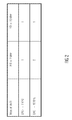
- FIG. 2 shows an exemplary table with measurement values at the first mixer Mx-TI depending on the input choices of the first digital-to-analog converter DAC-I, and the first low pass filter LP-TI.
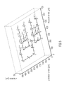
- FIG. 3 shows a perspective view of a circuit according to FIG. 1 in a system on package design.
- FIG. 4 shows exemplary input choices U(k,i) and corresponding measurement values Yd(k,m) generated by an embodiment of the invention.
- FIG. 5 shows an exemplary input table comprising all possible combinations of input choices U(k,i) and a second input table comprising random input choices U(k,i) generated by an embodiment of the invention.
- FIG. 6 shows the exemplary input table of FIG. 4 in an enumerated version of the input choice table of FIG. 4 and the deviations ⁇ Y(k,m) of the corresponding measurements as shown in FIG. 4 across D devices generated by an embodiment of the invention.
- FIG. 7 shows the table of FIG. 2 comprising additionally exemplary measurement values for a faulty device.
- FIG. 8 shows the exemplary input choices U(k,i) of FIG. 4 and measurement values Y(k,m) of the faulty device generated by an embodiment of the invention.
- FIG. 9 shows normalized input choices V(k,i) derived from the input choices U(k,i) of FIG. 8 , and normalized deviation values Z(k,m) derived from the measurement values Y(k,m) of FIG. 8 .
- FIG. 10 shows an exemplary relevance matrix R(i,m) generated by an embodiment of the invention.
- FIG. 11 shows the perspective view of FIG. 3 and the distance L of a location (450,500,0) to the signal path from the first stimulus node DAC-I to the third measurement node PA.
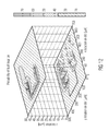
- FIG. 12 shows an exemplary fault location probability representation generated by an embodiment of the present invention with knowledge of the signal paths.
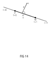
- FIG. 14 shows a location x and its distance d to a line segment of a signal path.
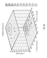
- FIG. 16 shows an exemplary fault location probability generated by an embodiment of the present invention without knowledge of the location of the signal paths.
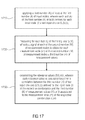
- FIG. 17 shows a flowchart of an embodiment of a method for determining relevance values R(i,m) for a detection of a fault on a chip.
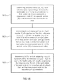
- FIG. 18 shows a flowchart of an embodiment of a method for determining a fault probability of a location on a chip.
- Stimuli typically “stimulate” or generate a signal to sensitize a potential fault.
- Stimuli can, for example, be:
- stimulus nodes The locations, where the stimuli are supplied either internal or external, are referred to as stimulus nodes.
- the second type of inputs, the conditions, influence the fault detectability by influencing a signal on a signal path from a stimulus node to a measurement node.
- Conditions can, for example, be:
- condition nodes Locations where these condition inputs are applied are referred to as condition nodes or, in general, input nodes. Both, stimulus nodes and condition nodes, are also referred to as input nodes. Furthermore, stimuli are also referred to as stimulus inputs, stimulus input choices or signals, and conditions as conditions inputs, input choices or parameters, wherein both stimuli and conditions are, in general, also referred to as inputs, test inputs or test input choices.
- the term “choice” only indicates that typically these inputs are chosen or selected from a plurality of possible inputs.
- the stimuli and conditions can be modeled, for example, as one of the following:
- waveforms are typically modeled as choices from available waveforms, for example, as explained above for the enumerated types, and not as arrays.
- measurement nodes The locations, where the measurements are performed, or in other words, where values of signals are measured, are referred to as measurement nodes.
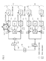
- FIG. 1 shows an exemplary diagram of a radio frequency (RF) transceiver circuit with 4 inputs or input nodes and 8 measurements or measurement nodes.
- the transmitter or transmitter part 110 of the transceiver 100 comprises a first digital-to-analog converter DAC_I 112 for converting digital I-signals to analog I-signals, a second digital-to-analog converter DAC_Q 114 for converting digital Q-signals to analog Q-signals, a phase locked loop PLL 116 , a first low pass filter LP_TI 118 for low pass filtering of the analog I-signal, a second low pass filter LP_TQ 120 for low pass filtering the analog Q-signal, a phase-shifter 122 , a first mixer Mx-TI 124 , a second mixer Mx-TQ 126 , a summer S 128 , and a power amplifier PA 130 .
- DAC_I 112 for converting digital I-signals to analog I-signals
- the receiver or receiver part 140 comprises a low noise amplifier LNA 142 , a second phase locked loop 144 , a second phase-shifter 146 , a third mixer Mx-RI 148 , a fourth mixer Mx-RQ 150 , a first analog-to-digital converter ADC_I 152 for converting an analog I-signal to a digital I-signal, and a second analog-to-digital converter ADC_Q 154 for converting an analog Q-signal to a digital Q-signal.
- the transceiver circuit 100 comprises an attenuator element Att 160 .
- the arrows in FIG. 1 show the signal paths from the different circuit elements of the transceiver circuit 100 and the direction of the respective signal flow.
- an output port of the first digital-to-analog converter DAC_I 112 is connected to an input port of the first low pass filter LP_TI 118
- an output port of the second digital-to-analog converter DAC_Q 114 is connected to an input port of the second low pass filter LP_TQ 120
- an output port of the phase locked loop 116 is connected to an input port of the phase-shifter 122
- an output port of the first low pass filter LP_TI 118 and a 0° output port of the phase-shifter 122 are connected to input ports of the first mixer Mx-TI 124
- a 90° output port of the phase-shifter 122 are connected to input ports of the second mixer Mx-TQ 126
- an output port of the first mixer Mx-TI 124 is connected to input ports of the summer S 1
- the attenuator element 160 providing the reception signal RX is connected to an input port of the low noise amplifier 142 , an output port of the low noise amplifier 142 is connected to an input port of the third mixer Mx-RI 148 , and to an input port of the fourth mixer Mx-RQ 150 , an output port of the second phase locked loop PLL 144 is connected to an input port of the second phase-shifter 146 , a 0° output port of the phase of the second phase-shifter 146 is connected to another input port of the third mixer 148 , a 90° output port of the second phase-shifter 146 is connected to a further input port of the fourth mixer 150 , an output port of the third mixer 148 is connected to an input port of the third low pass filter 152 , an output port of the fourth mixer 150 is connected to an input port of the fourth low pass filter LP_RQ 154 , an output port of the third low pass filter 152 is connected to the first analog-to-digital converter A
- FIG. 1 four exemplary input nodes are shown, see numbers 1 to 4 in dotted circles in FIG. 1 , that will also be referred to as first to fourth input nodes or 1 ′′ to 4 ′′ within the description.
- the 8 measurement nodes shown in FIG. 1 see numbers 1 to 8 in broken line squares will also be referred to as first to eight measurement node or 1 ′ to 8 ′ in the following description.
- the input nodes 1 ′′ and 2 ′′ are stimulus nodes, wherein the position of the input node 1 ′ corresponds to the position of the output port of the first digital-to-analog converter DAC_I 112 , or may correspond more general, to the position of the first digital-to-analog converter DAC_I 112 itself, and the position of the second input node 2 ′′corresponds to the location of the output port of the second digital-to-analog converter DAC_Q 114 , or may correspond more general, to the location of the second digital-to-analog converter DAC_Q 114 itself.
- the input nodes 3 ′′ and 4 ′′ are condition nodes, wherein the position of the input node 3 ′′ corresponds to the position of the first low pass filter 118 , and wherein the position of the input node 4 ′′corresponds to the position of the second low pass filter 120 .
- the position of the measurement node 1 ′ corresponds to the position of the output port of the first mixer 124 or the position of the first mixer 124 itself
- the position of the second measurement node 2 ′ corresponds to the position of the output port of the second mixer or the mixer 126 itself
- the position of the third measurement node 3 ′ corresponds to the position of the output port of the power amplifier 130 or the position of the power amplifier 130 itself.
- the position of the fourth measurement node 4 ′ corresponds to the position of the output node of the low noise amplifier 142 , or to the position of the low noise amplifier 142 itself
- the position of the fifth measurement node 5 ′ corresponds to the position of the output port of the third mixer 148 or the position of the third mixer 148 itself
- the position of the sixth measurement node 6 ′ corresponds to the position of the output port of the fourth mixer 150 or the position of the fourth mixer 150 itself
- the position of the seventh measurement node 7 ′ corresponds to the position of the input node of the first analog-to-digital converter ADC_I 156 or to the position of the first analog-to-digital converter 156 itself
- the position of the eighth measurement node 8 ′ corresponds to the position of the input port of the second analog-to-digital converter ADC_Q 158 or to the position of the second analog-to-digital converter 158 itself.
- each of the input nodes and measurement nodes is associated to a specific circuit element of the transceiver circuit, for example, the first input node is associated to the first digital-to-analog converter 112 .
- the localization of a faulty circuit element is facilitated, as will be described later.
- the digital-to-analog converters (DAC) 112 , 114 generate a 1 MHz or 10 MHz tone with an amplitude value of “1”
- the low pass filters (LP) invariably pass a 1 MHz tone and pass a 10 MHz tone only when in a 20 MHz mode
- the first mixer Mx-I 124 and the second mixer Mx-TQ 126 sum the passing tones' amplitudes.
- the sum of the passing tones' having an amplitude with values 0 or 1 is measured, as can be seen from FIG.
- FIG. 2 shows the table for the signal values measured at the output port of the first mixer Mx-TI 124 according to the aforementioned simplified device functionality in dependence on the test input applied at the first input node 1 ′′, being a stimulus node, by which the 1 MHz or 10 MHz tone generated by the first digital-to-analog converter 112 is applied, and for the two nodes of the first low pass filter LP-TI 118 , either applying the 2 MHz or the 20 MHz mode.
- the test input applied at the first input node 1 ′′ being a stimulus node, by which the 1 MHz or 10 MHz tone generated by the first digital-to-analog converter 112 is applied, and for the two nodes of the first low pass filter LP-TI 118 , either applying the 2 MHz or the 20 MHz mode.
- the 1 MHz tone applied at the first input node 1 ′′ from the first digital-to-analog converter 112 is passed without attenuation, whereas the 10 MHz tone passes unattenuated, see value “1” measured at the first mixer Mx-TI 124 , when the first low pass filter LP-TI 118 has a 20 MHz tone, and is completely blocked, see value “0” measured at the first mixer Mx-TI 124 , when the first low pass filter LP-TI 18 is in the 2 MHz mode.
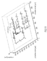
- FIG. 3 shows a realization of the transceiver circuit according to FIG. 1 as a “system in package” (SIP) implementation comprising a first or lower chip or die of 50 ⁇ m thickness and a second chip or die mounted on top of the first chip respective die.
- SIP system in package
- the signal path segment 302 can be described by nodes 16 and 17
- signal path segment 304 by nodes 17 and 18 .
- the graph of the circuit thus, can be described by its signal path segments or node connections, e.g. ⁇ . . . ,( 16 , 17 )( 17 , 18 ) . . . ⁇ .
- the first input node 1 ′′ corresponds to node 1
- the second input node 2 ′′ corresponds to node 2
- the third input node 3 ′′ corresponds to node 3
- the fourth input node 4 ′′ corresponds to node 4
- the first measurement node 1 ′ corresponds to node 5
- the second measurement node 2 ′ corresponds to node 6
- the first phase locked loop PLL corresponds to node 7
- the first phase-shifter 122 corresponds to node 8
- the third measurement node 3 ′ corresponds to node 13
- the fourth measurement node 4 ′ corresponds to node 17
- the fifth measurement node 5 ′ corresponds to node 22
- the sixth measurement node corresponds to node 23
- the seventh measurement node 7 ′ corresponds to node 26
- the eighth measurement node 8 ′ corresponds to node 27 .
- the circuit part of the transceiver circuit 100 implemented on the upper die is connected by an up-link, defined by nodes 11 and 12 , and a down-link defined by nodes 18 and 19 , to the circuit part of the transceiver circuit implemented on the lower die.
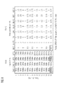
- FIG. 4 shows, on the left-hand-side, an exemplary test input matrix U for the transceiver circuit according to FIG. 1 and the further simplifying assumptions described, based on FIGS. 1 and 2 .
- the test input matrix U or Uk ⁇ I 410 is a K ⁇ I-matrix, with K being the number of tests and I being the number of different input nodes.
- a test input scenario or, a short input scenario, UK ⁇ I 410 comprises K tests, see the rows of the matrix, wherein each test k of K tests specifies for each input node i of I input nodes, an input choice j of J possible input choices, wherein the input choice j is the content contained in the matrix element specified by the test index and the input index i.
- the measurements or measurement values Yd(k,m) can also be represented in the form of a measurement table or matrix YK ⁇ M, respectively Yd, 460 that comprises for each test k of the K tests, see rows of the matrix, the signal value measured at each measurement node m of the M measurement nodes, see columns of the matrix.
- the measurement matrix Yd contains for each test, represented by the test index k (rows of the matrix), and for each of the measurement nodes, represented by the measurement index m (see columns of the matrix), the respective signal value measured at respective measurement node m during test k.
- test indices k from 1 to 16 are shown, whereas instead of the input indices i and the measurement indices m, the respective circuit elements according to FIG. 1 are shown.
- both digital-to-analog converters DAC-I and DAC-Q apply a 1 MHz tone as input choice, and both low pass filters LP-TI and LP-TQ are in or apply the 2 MHz mode as input choice, so that the 1 MHz signals pass the two low pass filters unattenuated.
- the tested device is a “good device” with no faults
- the signal value “1” is measured.
- the power amplifier PA measures the sum of the values provided by the two mixers Mx-TI and Mx-TQ divided by 2, so that at measurement node 3 ′ also the value “1” is measured.
- the first digital-to-analog converter DAC-I applies a 10 MHz tone
- the second digital-to-analog converter DAC-Q applies a 1 MHz tone
- both low pass filters LP-TI and LP-TQ apply the 2 MHz mode as input choice.
- the first mixer Mx-TI filters the 10 MHz signal
- only the second mixer Mx-TQ passes a signal with a signal value of “1” to the summer S 128 and the power amplifier PA 130 .
- the power amplifier PA measures the sum of the filtered signals divided by 2, so that at the third measurement node PA, only a value of 0.5 is measured.
- the following measurement nodes return the same value, i.e. 0.5 as the power amplifier PA.
- both digital-to-analog converters DAC-I and DAC-Q apply a 10 MHz tone as input choice and both low pass filters LP-TI and LP-TQ apply the 20 MHz mode as input choice, so that both 10 MHz signals are passed to the two mixers Mx-TI and Mx-TQ, where at each mixer the signal value “1” is measured, and accordingly, also at the power amplifier PA (see FIG. 4 : 20 MHz LP filter passes 10 MHz tone).
- test input choices U(k,i) or input scenario U can be defined by test engineers based on, for example, experience, knowledge about typical critical paths or circuit elements, or can be generated automatically in the sense of an automatic test program generation (ATPG). These automatically generated or selected input choices can be based on random choices, see for example the test input choice U(k,i) on the right-hand side of FIG. 5 , or may include all possible combinations of test input choices, see the example of U(k,i) on the left-hand-side of FIG. 5 . Within the automatic generation of test input choices, illegal, meaningless, or duplicate combinations can be removed.
- a first set of tests can be generated by test engineers and then enhanced by a second set of automatically generated input choices, to generate in an efficient manner a complete test scenario.
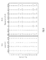
- FIG. 6 shows, on the right-hand side, exemplary average measurements ⁇ Y(k,m), that can be represented in the form of an average measurement matrix ⁇ Y,K ⁇ M like the individual measurement matrices YK ⁇ M as described based on FIG. 4 .
- these individual measurement matrices of the devices d will also be referred to as Yd(k,m).
- the average measurement matrix ⁇ Y comprises for each of the K tests, see rows of the matrix, an average signal value for each measurement node m of the M measurement nodes obtained by applying the same input scenario U(k,i) on the D good devices.
- DUT device under test
- the measured values at the first measurement node Mx-TI for devices with “no fault” are shown on the left side of the comma, whereas the measured values for the abovementioned defective device with the abovementioned “fault” are shown on the right side of the comma.
- the measured values for “no fault” correspond to the values as shown in FIG. 2 .
- the fault only appears, in case the first stimulus node DAC-I applies the 10 MHz tone and the first condition node LP-TI applies the 20 MHz mode.
- the fault is sensitized by the first input node DAC-I applying the second input choice, and is only detectable, in case the first condition node LP-TI applies the second input choice.
- This fault of ⁇ 6 dB at 10 MHz is also shown in FIG. 1 (see the star and reference sign 710 in FIG. 1 ).
- the input scenario U as already used for the characterization is shown.
- the measurements Y(k,m) of the faulty device are shown.
- the first stimulus node DAC-I applies the 10 MHz tone
- the first condition node LP-TI applies the 20 MHz mode, where the 10 MHz tone should normally pass without attenuation.
- the faulty 20 MHz LP filter LP-TI passes only half of the 10 MHz tone, as can be seen from the measured value at the first measurement node Mx-TI for the 16th test, i.e.
- Y(16,1) 0.5.
- the measurements at the second measurement node Mx-TQ are not influenced by the fault, because up to this measurement node, the signals of the first stimulus node and the second stimulus node are on different and independent signal paths.
- measurements and inputs are made comparable, before the correlation, by normalizing the deviations from their standard deviations.
- the inputs U(k,i) of the input scenario are normalized to deviations from their standard deviations across all tests k(I . . . K).
- This normalized input scenario VK ⁇ I can be pre-computed as part of the characterization.
- V(k,i) are the normalized input choices.
- the expected or average measurement value ⁇ Y(k,m) for each measurement node m under each test k across all D devices and the corresponding standard deviation ⁇ Y(k,m) can also be pre-computed as part of the characterization, like ⁇ U, ⁇ u(i) and V(k,i).
- the normalized measurement value matrix Zk ⁇ I with its normalized measurement values Z(k,i) contains for the diagnosed device deviations of its measurement values from the respective average or expected values obtained during the characterization, wherein the deviation is additionally normalized by the standard deviation obtained during the characterization.
- FIG. 9 shows the normalized input scenario V with the normalized input choices V(k,i) on the left-hand side, and on the right-hand side the normalized measurements Z(k,m) according to the aforementioned equations and assumptions.
- an input i is relevant for a fault detection at measurement m when normalized inputs V(k,i) correlate strongly with measurement deviations Z(k,m) and when the measurement deviations Z(k,m) are large.
- the fault relevance R(i,m) of input i to measurement m is proportional to the correlation C(i,m) with the column sums of C normalized to the absolute sum of the measurement deviations m. Certain embodiments calculate the respective relevance matrix R(i,m) as follows:
- the relevance matrix R for the measurement matrix Y respectively the normalized measurement deviation matrix Z of FIG. 9 is shown.
- the relevance matrix is calculated based on the aforementioned two equations for the calculation of the normalized correlation defining the fault relevance of input i to measurement m.
- R(1,1) and R(3,1) are the largest relevance values.
- the two pairs (DAC-I, Mx-TI) and (LP-TI, Mx-TI) are most relevant.
- the effect is only 50% of the effect for the two aforementioned input and measurement combinations.
- a high fault relevance R(i,m) indicates a high likelihood that a fault is close to the signal path from input i to measurement m, or through input i to measurement m.
- the diagnosed fault probability F(x,y,z) at die location (x,y,z), also referred to as Fault location probability F(x,y,z), is proportional to the sum of weighted distances L to the signal paths p from inputs i to measurement m, each weighted with relevance R(i,m) and divided by the number of paths P(i,m).
- L((x,y,z),i,m,p) is the distance from location (x,y,z) to the p-th path from input i to measurement m.
- the half-decay length L0 is the desired location resolution.
- FIG. 11 an example for a path p and a distance of a point from this path is shown.
- the fault probability F(x,y,z) is calculated for all, or at least all relevant locations (x,y,z), and can for example be presented in a color coded fault location probability distribution, where different colors as assigned to different fault location probabilities.
- FIG. 12 on the right-hand side, instead of a color coded probability indication, four different fault location probability ranges are depicted by using four different kinds of hashes. As can be seen from FIG. 12 , the fault location probability is the largest for areas along the signal path between the faulty third input node LP-TI and the first measurement node Mx-TI, and is still very high up to the third measurement node PA.
- Embodiments facilitate the diagnosis of suspicious design structures.
- Certain embodiments of the present invention allow not only the testing of known design structures but also the test of, for example failure prone, third party design structures, such as intellectual property (IP) blocks, amplifier designs, etc.
- IP intellectual property
- a fuse design view based on the layout, in combination with the fault probability view, as shown in FIG. 12 can support human “correlation” to locate faults faster or easier.
- the localization of suspicious design structures can be performed algorithmic by correlating (x,y,z) locations of specific design structures, for example, the circuit elements of the transceiver circuit of FIG. 1 with fault location probabilities (x,y,z). Areas with no design structure comprise the value “0” and locations with a design structure are associated with the value “1”. Thus, the failure location probability distribution as shown in FIG. 12 is focused on the locations of actual circuit elements and, eventually signal paths. The highest correlation indicates the most suspicious design structure.
- Embodiments of the present invention support the diagnosis of non-visible defects and do not need a physical fault analysis.
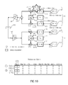
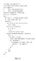
- FIG. 13 shows an embodiment of a recursive search algorithm through a directed graph for all paths from node n 1 to n 2 to find paths in a graph.
- the recursive search algorithm has the following structure:
- the distance to a path equals the closest distance d to any of the line segments between subsequence nodes from the path start node to the path end node.
- FIG. 14 shows the distance d to a line segment point by the nodes x 1 and x 2 .
- FIG. 15 shows a search algorithm for determining the closest distance from a point x and an n-dimensional space to a polygon or a line segment of a polygon.
- Certain embodiments of the present invention are implemented to use a straight signal path from input i to measurement m, when the signal path is not known.
- the assumption of a straight signal path from input i to measurement m is reasonable for many radio frequency circuits.
- FIG. 16 shows the fault location probability distribution F(xy,z) for a diagnosis of the faulty radio frequency transceiver according to FIGS. 1 and 3 , when the signal path is not known and cannot be used for determining the distance to the signal path.
- straight signal paths can be assumed between inputs i and measurements m.
- the distance L((x,y,z),i,m,p) and their fault location probability F(x,y,z) are calculated, based on these straight signal paths.
- the fault location probability F(x,y,z) is the highest for the faulty third input node LP-TI. This proves that also with no knowledge of the signal graph, helpful indications of the fault location can be obtained by embodiments of the present invention.
- FIG. 17 shows a flowchart of an embodiment of a method for determining relevance values R(i,m), each relevance value representing a relevance of a combination (i,m) of an input node i of a first number I of input nodes with a measurement node m of a second number M of measurement nodes for a detection of a fault on a chip.
- the method comprises the following steps.
- Embodiments of the method can implement the step 1730 for determining the relevance value such that for the calculation of the correlation each measurement value Y(k,m) is normalized with regard to an average value ⁇ Y(k,m) associated to the same test k and the same measurement node m as the measurement value Y(k,m).
- Embodiments of the method can further implement the step 1730 for determining the relevance value such that for the calculation of the correlation each measurement value Y(k,m) is normalized with regard to a standard deviation ⁇ Y(k,m) associated to the same test k and the same measurement node m as the measurement value Y(k,m).
- Embodiments of the method can implement the step 1730 for determining the relevance value such that the normalized measurement values Z(k,i) are calculated as follows:
- the normalization of the measurement values can include the calculation of the difference between the measurement values Y(km) and their respective average values ⁇ Y(k,m) and/or the division of the measurement values or of the aforementioned differences by the respective standard deviations ⁇ Y(k,m) to improve the correlation result, or can use other algorithms to calculate an average value or equivalents for the standard deviation to obtain similar results.
- Embodiments of the method can further implement the step 1730 for determining the relevance value such that for the calculation of the correlation each test input choice U(k,i) is normalized with regard to an average value ⁇ U(i) associated to the same input node i as the test input choice U(k,i), wherein the average value ⁇ U(i) is an average value of the third plurality K of test input choices associated to the input node i.
- Embodiments of the method can further implement the step 1730 for determining the relevance value such that for the calculation of the correlation each test input choice U(k,i) is normalized with regard to a standard deviation ⁇ U(i) associated to the same input node i as the test input choice (U(k,i)), wherein the standard deviation ( ⁇ U(i)) is a standard deviation of the third plurality (K) of test input choices associated to the input node (i).
- Embodiments of the method can implement the step 1730 for determining the relevance value such that the normalized test input choices V(k,i) are calculated as follows:
- the normalization V(k,i) of the test input choices can include the calculation of the difference between the individual input choices U(k,i) and the respective average values ⁇ U(i) calculated across the respective column i of the test input matrix U and/or the division of the test input choices L(k,i) or of the aforementioned differences by the respective standard deviations ⁇ U(i) calculated across the respective column i of the test input matrix U to improve the correlation results, or can use other algorithms to calculate an average value or equivalents for the standard deviation to obtain similar results.
- the average values and the standard deviations can be predetermined or pre-computed during the characterization phase, so that for the later diagnosis these pre-computed values can be provided to reduce the processing power requirements for the diagnosis.
- Embodiments of the method can implement the step 1730 for determining the relevance value such that the correlation value C(i,m) obtained by the correlation is already the relevance value R(i,m) used for a further diagnosis without the need for further calculations.
- Embodiments of the method can implement the step 1730 for determining the relevance value such that the correlation values C(i.m) are calculated as follows:
- V(k,i) are the test input choices U(k,i) normalized to average values ⁇ U(i) and standard deviations ⁇ U(i) associated to the same input node i calculated across all K input choices for the respective input node i
- Z(k,m) are the measurement values Y(k,m) normalized to average values ⁇ Y(k,m) and standard deviations ⁇ Y(k,m) associated to the same test k and the same measurement node m obtained across the D tests during characterization.
- Embodiments of the method can implement the step 1730 for determining the relevance value such that the fault relevance values R(i,m) are determined at follows:
- Z(k,m) is a measurement value Y(k,m) normalized to deviations from its standard deviation across all K test input choices
- C(i,m) is the correlation value between input node i and measurement node m of the device under test.
- embodiments can be adapted to calculate a fault relevance R(i,m) of each input node i to each measurement m that is proportional to the correlation value C(i,m), with the column sums of the correlation matrix C normalized to the absolute sum of measurement deviations m.
- Alternative embodiments can be adapted to calculate the relevance values, generally speaking, based on the correlation values C(i,m) and a weighting factor, wherein the weighting factor is calculated such that it depends on a sum of the K measurement deviations Z(k,m) associated to the same measurement node m and/or is the higher the measurement deviations Z(k,m) associated to the same measurement node m are, and/or wherein the weighting factor depends on a sum of correlation values C(i,m) associated to the same measurement node m and/or is the lower the higher the correlation values C(i,m) associated to the same measurement node m are.
- the relevance matrix R or even individual relevance values R(i,m) can already provide sufficient information for at least narrowing down the localization of the fault.
- FIG. 18 shows a flowchart of an embodiment of a method for determining a fault probability for a location on a chip. The method comprising the following steps.
- each relevance value representing a relevance of a combination (i,m) of an input node i of a first number I of input nodes with a measurement node (m) of a second number M of measurement nodes for a detection of a fault on a chip.
- Determining 1830 the fault probability F(x,y,z) based on adding the distances L((x,y,z), i,m,p) to each of the fourth number P of paths weighted by the relevance value R(i,m) of the combination of the input node i, the respective path p extends from, and the measurement node m the respective path p extends to.
- Embodiments of the method can implement the step 1830 for determining the fault probability F(x,y,z) based on the following algorithm:
- P(i,m) is the number of paths from input node i to measurement node m
- R(i,m,) is the relevance value of the combination (i,m) of an input node i with a measurement node m
- L((x,y,z),i,m,p) is the distance from location (x,y,z) to the p-th path from input node i to measurement m
- L0 is the half-decay length defining the location resolution.
- embodiments of the inventions can be adapted to use this information for the calculation of the distance L providing a position information for each input node i.
- the position of the signal paths can, for example, be defined by providing for each path p of the fourth number of paths a plurality of further nodes to define the position of the path p or segment of the path between the position of the input node i and the position of the measurement node m (see FIGS. 3 and 11 ).
- these paths p can be assumed to be straight lines between the position of the input node i and the position of the measurement node m defining the signal path.
- Embodiments of the invention can be implemented to calculate the fault location probabilities for all or at least all relevant locations on the chip to obtain a fault location distribution of as shown in FIGS. 12 and 16 .
- Such a color coded presentation for example, together with a presentation of the positions of the circuit elements provides a usefuld means for localizing faults or at least error prone regions of a chip design.
- Embodiments of the invention can be further implemented to additionally correlate the fault probability F(x,y,z) of each location (x,y,z) with an position indicator, the position indicator having different values for locations (x,y,z) of the chip, for example “0” for positions with no circuit element and “1” for positions with a circuit element, to, thus, focus the fault localization to locations where input nodes, measurement nodes or signal paths are positioned.
- Embodiments of an apparatus for determining the relevance values describing a relevance of I input nodes for a fault detection at M measurement nodes of a chip comprise at least one input port for receiving the measurement values Y(k,m), for receiving the expected or average values ⁇ Y(k,m), the standard deviations ⁇ Y(k,m) and the corresponding input choices U(k,i) or normalized input choices V(k,i), and an output port for providing at least the correlation C(i,m) or relevance values R(i,m). Further embodiments can comprise at least one additional input port for applying the test choices U(k,i) to the device under test, or in other words, to connect the apparatus with the device under test for the characterization and/or the diagnosis.
- Further embodiments of the apparatus are additionally implemented to determine the fault probability of a location based on known locations of the input nodes and measurement nodes. Even further embodiments of the present application are implemented to determine the fault probability of a location on the chip based on the additional knowledge about the location of the signal graphs connecting the input nodes with the measurement nodes.
- Embodiments of the apparatus adapted to determine the fault probability can also comprise an output port for providing the fault probability for some or all of the 2-dimensional locations (x,y) or 3-dimensional locations (x,y,z), for example as shown in FIG. 12 or 16 .
- inventions of the apparatus may also be implemented to perform the characterization by performing the tests for D good, or essentially good devices to calculate the expected values ⁇ Y(k,m) and the standard deviations ⁇ Y(k,m) and to output the input choices U(k,i) for normalized input choices V(k,i).
- Embodiments of the apparatus adapted to perform the characterization can comprise user interfaces for defining the input nodes, measurement nodes and/or input choices, or to select certain input nodes, measurement nodes and/or input choices from an available set of input nodes, measurement nodes and/or input choices. Further embodiments of the invention can be adapted to select or choose input nodes, measurement nodes and/or input choices from a given set of nodes or ranges, or sets of input choices automatically.
- the “Characterization” can be performed, for example, by development or test engineers once, when the product is designed, for example, in a pre-series production, based on testing true devices (no simulation).
- the “Diagnosis” of the devices can be performed at the mass production sites to control the quality and gain of the mass production, respectively to control a deviation or un-usuality within the mass production or to detect a design weakness by testing a plurality of faulty devices.
- Embodiments of the invention can be adapted to add, for example, the fault probabilities F(x,y,z) for each location of a plurality of faulty devices to facilitate the detection of design weaknesses of the chip or its circuit elements. Furthermore, error prone library elements can thus be detected. If for example, the fault location probability is not only high for a specific low pass filter LP_TI but also for the other low pass filters LP_TQ, LP_RI and LP-RQ, all defined by the same library element, a test engineer can derive that this element or module in general is error prone.
- Advantages of embodiments of the present invention are its simplicity, as no simulation is needed, as no access to a chip simulation model is needed, as no modeling of the test interaction is needed and as no lengthy (fault) simulations are needed.
- test combinations can be automatically generated.
- the approach of the invention is generic in that the device under test is modeled as a black box with a set of input choices U(k,i) and a set of output measurements Y(k,i).
- Embodiments of the invention provide a means for increasing the radio frequency coverage at wafer tests for PGD flows by enabling massive multi-site wafer tests on non-radio frequency equipment and/or by allowing to postpone performance tests of radio frequency tests to final tests.
- embodiments enable to diagnose design weaknesses in radio frequency circuits during high-volume manufacturing and/or to diagnose non-visible defects or weaknesses.
- the inventive methods can be implemented in hardware or in software.
- the implementation can be performed using a digital storage medium, in particular, a disc, CD or a DVD having an electronically readable control signal stored thereon, which cooperates with a programmable computer system, such that an embodiment of the inventive methods is performed.
- an embodiment of the present invention is, therefore, a computer program product with a program code stored on a machine-readable carrier, the program code being operative for performing the inventive methods when the computer program product runs on a computer.
- embodiments of the inventive methods are, therefore, a computer program having a program code for performing at least one of the inventive methods when the computer program runs of a computer.
Landscapes
- Engineering & Computer Science (AREA)
- General Engineering & Computer Science (AREA)
- Physics & Mathematics (AREA)
- General Physics & Mathematics (AREA)
- Computer Hardware Design (AREA)
- Microelectronics & Electronic Packaging (AREA)
- Health & Medical Sciences (AREA)
- Artificial Intelligence (AREA)
- Evolutionary Computation (AREA)
- Medical Informatics (AREA)
- Tests Of Electronic Circuits (AREA)
Abstract
Description
-
- supply voltages, e.g. Vdd
- external waveform generators
- internal digital-to-analog converters (DACs).
-
- gain or filter settings
- digital tuning words
- bypass modes
- Signal path selections, switches
- Correction DAC, e.g. offset correction
- Temperature.
-
- floating point numbers, e.g. supply voltage,
- integers, e.g. DAC code word,
- Boolean,
- Enumerate types, e.g. the stimulus being a fast sine, slow sine or ramp function, wherein the enumerated types are modeled as multiple Boolean inputs at the same location.
-
- external supply current measurement, e.g. Iddq
- built-in current or power or speed sensor
- THD value from a captured waveform
- Over-range detected: “yes”=+1 or “no”=−1.
- a) information about the nodes like name and location of the node, for example, for node n=9: Name: DAC-I, Location: (600,400,0);
- b) information about inputs (i=1 . . . 4) like node number and stimulus or condition choices, for example, for input i=3: Node: n=3, Choices (2 MHz, 20 MHz):
- c) information about the measurements (m=1 . . . 8) like measurement index and node number or node index, for example, for m=8: Node: 27;
- d) information about the graph and the node connections, for example, { . . . ,(16,17),(17,18), . . . }.
- 1. Start with n=n1.
- 2. Get all nodes connected to n.
- 3. Stop when there are no nodes connected to n.
- 4. When only one node connected, continue at 2. with connected node.
- 5. When multiple nodes are connected, recursively gather all connected sub-paths.
wherein Y(k,m) is a measurement value associated to a test k and a measurement node m, μY(k,m) is the expected or average measurement value for test k and measurement node m over all D devices obtained during the characterization, wherein σY(km) is the standard deviation of the measurement value obtained for test k and measurement node m over all D devices obtained during characterization.
wherein U(k,i) are the test input choices associated to an input node i, μU(i) is the average value over all K test input choices for input node I calculated, and wherein σU(i) is the standard deviation for input node i over all K input choices for input node i.
wherein i is the index of the input nodes with i=1 . . . I, m is the index for the measurement nodes with m=1 . . . M, k is the index for the tests with k=1 . . . K, wherein V(k,i) are the test input choices U(k,i) normalized to average values μU(i) and standard deviations σU(i) associated to the same input node i calculated across all K input choices for the respective input node i, and Z(k,m) are the measurement values Y(k,m) normalized to average values μY(k,m) and standard deviations σY(k,m) associated to the same test k and the same measurement node m obtained across the D tests during characterization.
wherein i is the index of the input nodes with i=1 . . . I, m is the index for the measurement nodes with m=1 . . . M, k is the index for the tests with k=1 . . . K, wherein Z(k,m) is a measurement value Y(k,m) normalized to deviations from its standard deviation across all K test input choices, and wherein C(i,m) is the correlation value between input node i and measurement node m of the device under test.
wherein (x,y,z) is the location, wherein i is the index of the input nodes with i=1 . . . I, m is the index for the measurement nodes with m=1 . . . M, wherein P(i,m) is the number of paths from input node i to measurement node m, wherein R(i,m,) is the relevance value of the combination (i,m) of an input node i with a measurement node m, wherein L((x,y,z),i,m,p) is the distance from location (x,y,z) to the p-th path from input node i to measurement m, and wherein L0 is the half-decay length defining the location resolution.
Claims (6)
Priority Applications (1)
| Application Number | Priority Date | Filing Date | Title |
|---|---|---|---|
| US14/295,293 US9658282B2 (en) | 2008-12-17 | 2014-06-03 | Techniques for determining a fault probability of a location on a chip |
Applications Claiming Priority (3)
| Application Number | Priority Date | Filing Date | Title |
|---|---|---|---|
| PCT/EP2008/010787 WO2010069344A1 (en) | 2008-12-17 | 2008-12-17 | Method and apparatus for determining relevance values for a detection of a fault on a chip and for determining a fault probability of a location on a chip |
| US67167410A | 2010-11-01 | 2010-11-01 | |
| US14/295,293 US9658282B2 (en) | 2008-12-17 | 2014-06-03 | Techniques for determining a fault probability of a location on a chip |
Related Parent Applications (2)
| Application Number | Title | Priority Date | Filing Date |
|---|---|---|---|
| US12/671,674 Division US8745568B2 (en) | 2008-12-17 | 2008-12-17 | Method and apparatus for determining relevance values for a detection of a fault on a chip and for determining a fault probability of a location on a chip |
| PCT/EP2008/010787 Division WO2010069344A1 (en) | 2008-12-17 | 2008-12-17 | Method and apparatus for determining relevance values for a detection of a fault on a chip and for determining a fault probability of a location on a chip |
Publications (2)
| Publication Number | Publication Date |
|---|---|
| US20140336958A1 US20140336958A1 (en) | 2014-11-13 |
| US9658282B2 true US9658282B2 (en) | 2017-05-23 |
Family
ID=41011881
Family Applications (2)
| Application Number | Title | Priority Date | Filing Date |
|---|---|---|---|
| US12/671,674 Active 2030-08-16 US8745568B2 (en) | 2008-12-17 | 2008-12-17 | Method and apparatus for determining relevance values for a detection of a fault on a chip and for determining a fault probability of a location on a chip |
| US14/295,293 Active 2030-02-11 US9658282B2 (en) | 2008-12-17 | 2014-06-03 | Techniques for determining a fault probability of a location on a chip |
Family Applications Before (1)
| Application Number | Title | Priority Date | Filing Date |
|---|---|---|---|
| US12/671,674 Active 2030-08-16 US8745568B2 (en) | 2008-12-17 | 2008-12-17 | Method and apparatus for determining relevance values for a detection of a fault on a chip and for determining a fault probability of a location on a chip |
Country Status (7)
| Country | Link |
|---|---|
| US (2) | US8745568B2 (en) |
| JP (1) | JP2011505016A (en) |
| KR (1) | KR101118421B1 (en) |
| CN (1) | CN101821640B (en) |
| DE (1) | DE112008001173B4 (en) |
| TW (1) | TWI395959B (en) |
| WO (1) | WO2010069344A1 (en) |
Families Citing this family (17)
| Publication number | Priority date | Publication date | Assignee | Title |
|---|---|---|---|---|
| JP2011505016A (en) | 2008-12-17 | 2011-02-17 | ヴェリジー(シンガポール) プライベート リミテッド | Method and apparatus for determining relevance value for defect detection of chip and determining defect probability at position on chip |
| US8402421B2 (en) * | 2010-10-12 | 2013-03-19 | Cadence Design Systems, Inc. | Method and system for subnet defect diagnostics through fault compositing |
| JP6320862B2 (en) * | 2014-07-15 | 2018-05-09 | 日置電機株式会社 | Inspection apparatus and inspection method |
| US9569577B2 (en) * | 2014-10-15 | 2017-02-14 | Freescale Semiconductor, Inc. | Identifying noise couplings in integrated circuit |
| US9990248B2 (en) * | 2015-04-07 | 2018-06-05 | Samsung Electronics Co., Ltd. | Display driver integrated circuit and display device having the same |
| DE102016225081A1 (en) * | 2016-12-15 | 2018-06-21 | Robert Bosch Gmbh | Apparatus and method for determining the pinpoint capability of possible errors of one or more components |
| WO2018162050A1 (en) * | 2017-03-07 | 2018-09-13 | Advantest Corporation | Tester and method for testing a device under test using relevance scores |
| WO2018162049A1 (en) * | 2017-03-07 | 2018-09-13 | Advantest Corporation | Test apparatus for performing a test on a device under test and data set filter for filtering a data set to obtain a best setting of a device under test |
| WO2018162047A1 (en) | 2017-03-07 | 2018-09-13 | Advantest Corporation | Tester and method for testing a device under test and tester and method for determining a single decision function |
| CN107070703A (en) * | 2017-03-20 | 2017-08-18 | 同济大学 | A kind of 2D MESH network-on-chip switch test methods based on path analysis |
| CN107966648B (en) * | 2017-11-27 | 2019-10-01 | 中国航空综合技术研究所 | A kind of embedded failure diagnosis method based on correlation matrix |
| CN111656715B (en) * | 2018-06-04 | 2022-01-11 | Oppo广东移动通信有限公司 | Codebook processing method, system, network equipment, user equipment and storage medium |
| CN109030983B (en) * | 2018-06-11 | 2020-07-03 | 北京航空航天大学 | Diagnostic relation matrix generation method considering excitation test |
| US10536226B1 (en) * | 2018-07-16 | 2020-01-14 | Litepoint Corporation | System and method for over-the-air (OTA) testing to detect faulty elements in an active array antenna of an extremely high frequency (EHF) wireless communication device |
| CN112653577A (en) * | 2020-12-14 | 2021-04-13 | 武汉绿色网络信息服务有限责任公司 | Network element management method, device and storage medium |
| US11614480B2 (en) * | 2021-06-08 | 2023-03-28 | Kla Corporation | System and method for Z-PAT defect-guided statistical outlier detection of semiconductor reliability failures |
| CN115128438A (en) * | 2022-09-02 | 2022-09-30 | 中诚华隆计算机技术有限公司 | Chip internal fault monitoring method and device |
Citations (18)
| Publication number | Priority date | Publication date | Assignee | Title |
|---|---|---|---|---|
| US4044244A (en) * | 1976-08-06 | 1977-08-23 | International Business Machines Corporation | Automatic tester for complex semiconductor components including combinations of logic, memory and analog devices and processes of testing thereof |
| US5241652A (en) * | 1989-06-08 | 1993-08-31 | Digital Equipment Corporation | System for performing rule partitioning in a rete network |
| US5655074A (en) * | 1995-07-06 | 1997-08-05 | Bell Communications Research, Inc. | Method and system for conducting statistical quality analysis of a complex system |
| US6054863A (en) * | 1996-09-11 | 2000-04-25 | International Business Machines Corporation | System for testing circuit board integrity |
| US20020143516A1 (en) * | 2001-02-16 | 2002-10-03 | Rao Guruprasad G. | Apparatus and methods for constraint characterization with degradation options |
| US6519727B2 (en) * | 1999-03-01 | 2003-02-11 | Verisity Ltd. | System and method for applying flexible constraints |
| US20040168100A1 (en) * | 2000-12-04 | 2004-08-26 | Thottan Marina K. | Fault detection and prediction for management of computer networks |
| US20040249577A1 (en) * | 2001-07-11 | 2004-12-09 | Harri Kiiveri | Method and apparatus for identifying components of a system with a response acteristic |
| US6950771B1 (en) | 2003-12-09 | 2005-09-27 | Xilinx, Inc. | Correlation of electrical test data with physical defect data |
| US20060156316A1 (en) * | 2004-12-18 | 2006-07-13 | Gray Area Technologies | System and method for application specific array processing |
| US20070233445A1 (en) * | 2004-05-10 | 2007-10-04 | Nibea Quality Management Solutions Ltd. | Testing Suite for Product Functionality Assurance and Guided Troubleshooting |
| US20070288822A1 (en) * | 2006-04-27 | 2007-12-13 | Xijiang Lin | Timing-aware test generation and fault simulation |
| US7454963B2 (en) * | 2003-10-09 | 2008-11-25 | Avl List Gmbh | Method for ensuring the reliability of technical components |
| US20080301597A1 (en) | 2007-05-29 | 2008-12-04 | International Business Machines Corporation | Method to Determine the Root Causes of Failure Patterns by Using Spatial Correlation of Tester Data |
| US7592818B2 (en) * | 2005-09-01 | 2009-09-22 | Murata Manufacturing Co., Ltd. | Method and apparatus for measuring scattering coefficient of device under test |
| US7620856B2 (en) * | 2006-12-28 | 2009-11-17 | Sap Portals Israel Ltd. | Framework for automated testing of enterprise computer systems |
| US7990887B2 (en) * | 2006-02-22 | 2011-08-02 | Cisco Technology, Inc. | Sampling test of network performance |
| US8745568B2 (en) | 2008-12-17 | 2014-06-03 | Advantest (Singapore) Pte Ltd | Method and apparatus for determining relevance values for a detection of a fault on a chip and for determining a fault probability of a location on a chip |
Family Cites Families (6)
| Publication number | Priority date | Publication date | Assignee | Title |
|---|---|---|---|---|
| JPH0572281A (en) * | 1991-09-13 | 1993-03-23 | Fujitsu Ltd | Measuring apparatus |
| US6842866B2 (en) | 2002-10-25 | 2005-01-11 | Xin Song | Method and system for analyzing bitmap test data |
| TWI286216B (en) * | 2004-06-29 | 2007-09-01 | Pixart Imaging Inc | Single chip test method, component and its test system |
| US7676077B2 (en) | 2005-11-18 | 2010-03-09 | Kla-Tencor Technologies Corp. | Methods and systems for utilizing design data in combination with inspection data |
| TWI298394B (en) * | 2006-03-15 | 2008-07-01 | Silicon Integrated Sys Corp | Method for detecting defects of a chip |
| JP5072281B2 (en) * | 2006-07-28 | 2012-11-14 | 株式会社キーエンス | Laser processing apparatus, laser processing condition setting apparatus, laser processing method, laser processing condition setting method, laser processing condition setting program |
-
2008
- 2008-12-17 JP JP2010542530A patent/JP2011505016A/en active Pending
- 2008-12-17 CN CN200880101430.5A patent/CN101821640B/en active Active
- 2008-12-17 US US12/671,674 patent/US8745568B2/en active Active
- 2008-12-17 WO PCT/EP2008/010787 patent/WO2010069344A1/en active Application Filing
- 2008-12-17 DE DE112008001173T patent/DE112008001173B4/en not_active Expired - Fee Related
- 2008-12-17 KR KR1020107002167A patent/KR101118421B1/en active IP Right Grant
-
2009
- 2009-12-08 TW TW098141872A patent/TWI395959B/en active
-
2014
- 2014-06-03 US US14/295,293 patent/US9658282B2/en active Active
Patent Citations (18)
| Publication number | Priority date | Publication date | Assignee | Title |
|---|---|---|---|---|
| US4044244A (en) * | 1976-08-06 | 1977-08-23 | International Business Machines Corporation | Automatic tester for complex semiconductor components including combinations of logic, memory and analog devices and processes of testing thereof |
| US5241652A (en) * | 1989-06-08 | 1993-08-31 | Digital Equipment Corporation | System for performing rule partitioning in a rete network |
| US5655074A (en) * | 1995-07-06 | 1997-08-05 | Bell Communications Research, Inc. | Method and system for conducting statistical quality analysis of a complex system |
| US6054863A (en) * | 1996-09-11 | 2000-04-25 | International Business Machines Corporation | System for testing circuit board integrity |
| US6519727B2 (en) * | 1999-03-01 | 2003-02-11 | Verisity Ltd. | System and method for applying flexible constraints |
| US20040168100A1 (en) * | 2000-12-04 | 2004-08-26 | Thottan Marina K. | Fault detection and prediction for management of computer networks |
| US20020143516A1 (en) * | 2001-02-16 | 2002-10-03 | Rao Guruprasad G. | Apparatus and methods for constraint characterization with degradation options |
| US20040249577A1 (en) * | 2001-07-11 | 2004-12-09 | Harri Kiiveri | Method and apparatus for identifying components of a system with a response acteristic |
| US7454963B2 (en) * | 2003-10-09 | 2008-11-25 | Avl List Gmbh | Method for ensuring the reliability of technical components |
| US6950771B1 (en) | 2003-12-09 | 2005-09-27 | Xilinx, Inc. | Correlation of electrical test data with physical defect data |
| US20070233445A1 (en) * | 2004-05-10 | 2007-10-04 | Nibea Quality Management Solutions Ltd. | Testing Suite for Product Functionality Assurance and Guided Troubleshooting |
| US20060156316A1 (en) * | 2004-12-18 | 2006-07-13 | Gray Area Technologies | System and method for application specific array processing |
| US7592818B2 (en) * | 2005-09-01 | 2009-09-22 | Murata Manufacturing Co., Ltd. | Method and apparatus for measuring scattering coefficient of device under test |
| US7990887B2 (en) * | 2006-02-22 | 2011-08-02 | Cisco Technology, Inc. | Sampling test of network performance |
| US20070288822A1 (en) * | 2006-04-27 | 2007-12-13 | Xijiang Lin | Timing-aware test generation and fault simulation |
| US7620856B2 (en) * | 2006-12-28 | 2009-11-17 | Sap Portals Israel Ltd. | Framework for automated testing of enterprise computer systems |
| US20080301597A1 (en) | 2007-05-29 | 2008-12-04 | International Business Machines Corporation | Method to Determine the Root Causes of Failure Patterns by Using Spatial Correlation of Tester Data |
| US8745568B2 (en) | 2008-12-17 | 2014-06-03 | Advantest (Singapore) Pte Ltd | Method and apparatus for determining relevance values for a detection of a fault on a chip and for determining a fault probability of a location on a chip |
Non-Patent Citations (3)
| Title |
|---|
| Fu, Qiang, et al., "Characterizing Intra-Die Spatial Correlation Using Spectral Density Method", 9th International Symposium on Quality Electronic Deisgn, Piscataway, New Jersey, 2008, pp. 718-723. |
| Liu, Fang, et al., "Efficient Simulation of Parametric Faults for Multi-Stage Analog Circuits", IEEE Test Conference 2007, Paper 24.2, pp. 1-9. |
| Varghese et al.; "Simplified ATPGand Analog Fault Location via Clustering and Separability Technique", IEEE Transactions on Circuits and Systems, vol. Cas-26, No. 7; Jul. 1979; pp. 496-505. |
Also Published As
| Publication number | Publication date |
|---|---|
| CN101821640A (en) | 2010-09-01 |
| TWI395959B (en) | 2013-05-11 |
| KR101118421B1 (en) | 2012-03-13 |
| WO2010069344A1 (en) | 2010-06-24 |
| US8745568B2 (en) | 2014-06-03 |
| JP2011505016A (en) | 2011-02-17 |
| TW201030357A (en) | 2010-08-16 |
| DE112008001173B4 (en) | 2012-12-20 |
| US20110032829A1 (en) | 2011-02-10 |
| DE112008001173T5 (en) | 2010-09-30 |
| CN101821640B (en) | 2015-03-11 |
| KR20100103449A (en) | 2010-09-27 |
| US20140336958A1 (en) | 2014-11-13 |
Similar Documents
| Publication | Publication Date | Title |
|---|---|---|
| US9658282B2 (en) | Techniques for determining a fault probability of a location on a chip | |
| Milor | A tutorial introduction to research on analog and mixed-signal circuit testing | |
| US10379168B2 (en) | Apparatuses and methods for testing electrochemical cells by measuring frequency response | |
| US7385410B2 (en) | Method of and apparatus for testing for integrated circuit contact defects | |
| US8103463B2 (en) | Systems and methods for predicting failure of electronic systems and assessing level of degradation and remaining useful life | |
| US7043389B2 (en) | Method and system for identifying and locating defects in an integrated circuit | |
| US20070033474A1 (en) | Production test technique for RF circuits using embedded test sensors | |
| Ayari et al. | Smart selection of indirect parameters for DC-based alternate RF IC testing | |
| Han et al. | Low-cost parametric test and diagnosis of RF systems using multi-tone response envelope detection | |
| Roberts | Metrics, techniques and recent developments in mixed-signal testing | |
| Banerjee et al. | Analog/RF built-in-self-test subsystem for a mobile broadcast video receiver in 65-nm CMOS | |
| US7206710B2 (en) | Incremental generation of calibration factors for automated test equipment | |
| US20060176048A1 (en) | Generation and use of calibration data for automated test equipment | |
| WO2012009477A1 (en) | Methods and apparatus for providing a built-in self test | |
| US20040148549A1 (en) | Method for using an alternate performance test to reduce test time and improve manufacturing yield | |
| US3102231A (en) | White noise fault detection system | |
| US6964004B2 (en) | Method and apparatus for testing a system-on-a-chip | |
| Gomes et al. | Minimal length diagnostic tests for analog circuits using test history | |
| Van Spaandonk et al. | Selecting measurements to test the functional behavior of analog circuits | |
| Deyati et al. | BISCC: Efficient pre through post silicon validation of mixed-signal/RF systems using built in state consistency checking | |
| CN111880073A (en) | Built-in test design method and system | |
| Liobe et al. | Fault diagnosis of a GHz CMOS LNA using high-speed ADC-based BIST | |
| Kabisatpathy et al. | Fault Diagnosis Methodology | |
| Bahukudumbi et al. | Wafer-Level Defect Screening for “Big-D/Small-A” Mixed-Signal SoCs | |
| Akbay | Constraint-driven RF test stimulus generation and built-in test |
Legal Events
| Date | Code | Title | Description |
|---|---|---|---|
| AS | Assignment |
Owner name: ADVANTEST CORPORATION, JAPAN Free format text: ASSIGNMENT OF ASSIGNORS INTEREST;ASSIGNOR:ADVANTEST (SINGAPORE) PTE. LTD.;REEL/FRAME:035375/0233 Effective date: 20150401 |
|
| AS | Assignment |
Owner name: ADVANTEST CORPORATION, JAPAN Free format text: CORRECTIVE ASSIGNMENT TO CORRECT THE ASSIGNEE'S ADDRESS PREVIOUSLY RECORDED AT REEL: 035375 FRAME: 0233. ASSIGNOR(S) HEREBY CONFIRMS THE ASSIGNMENT;ASSIGNOR:ADVANTEST (SINGAPORE) PTE. LTD.;REEL/FRAME:035444/0018 Effective date: 20150401 |
|
| STCF | Information on status: patent grant |
Free format text: PATENTED CASE |
|
| AS | Assignment |
Owner name: ADVANTEST CORPORATION, JAPAN Free format text: CHANGE OF ADDRESS;ASSIGNOR:ADVANTEST CORPORATION;REEL/FRAME:047987/0626 Effective date: 20181112 |
|
| MAFP | Maintenance fee payment |
Free format text: PAYMENT OF MAINTENANCE FEE, 4TH YEAR, LARGE ENTITY (ORIGINAL EVENT CODE: M1551); ENTITY STATUS OF PATENT OWNER: LARGE ENTITY Year of fee payment: 4 |