US9595606B2 - Field-effect transistor - Google Patents
Field-effect transistor Download PDFInfo
- Publication number
- US9595606B2 US9595606B2 US14/790,064 US201514790064A US9595606B2 US 9595606 B2 US9595606 B2 US 9595606B2 US 201514790064 A US201514790064 A US 201514790064A US 9595606 B2 US9595606 B2 US 9595606B2
- Authority
- US
- United States
- Prior art keywords
- layer
- semiconductor layer
- field
- effect transistor
- nitride semiconductor
- Prior art date
- Legal status (The legal status is an assumption and is not a legal conclusion. Google has not performed a legal analysis and makes no representation as to the accuracy of the status listed.)
- Active
Links
Images


Classifications
-
- H—ELECTRICITY
- H10—SEMICONDUCTOR DEVICES; ELECTRIC SOLID-STATE DEVICES NOT OTHERWISE PROVIDED FOR
- H10D—INORGANIC ELECTRIC SEMICONDUCTOR DEVICES
- H10D30/00—Field-effect transistors [FET]
- H10D30/40—FETs having zero-dimensional [0D], one-dimensional [1D] or two-dimensional [2D] charge carrier gas channels
- H10D30/47—FETs having zero-dimensional [0D], one-dimensional [1D] or two-dimensional [2D] charge carrier gas channels having two-dimensional [2D] charge carrier gas channels, e.g. nanoribbon FETs or high electron mobility transistors [HEMT]
- H10D30/471—High electron mobility transistors [HEMT] or high hole mobility transistors [HHMT]
- H10D30/475—High electron mobility transistors [HEMT] or high hole mobility transistors [HHMT] having wider bandgap layer formed on top of lower bandgap active layer, e.g. undoped barrier HEMTs such as i-AlGaN/GaN HEMTs
- H10D30/4755—High electron mobility transistors [HEMT] or high hole mobility transistors [HHMT] having wider bandgap layer formed on top of lower bandgap active layer, e.g. undoped barrier HEMTs such as i-AlGaN/GaN HEMTs having wide bandgap charge-carrier supplying layers, e.g. modulation doped HEMTs such as n-AlGaAs/GaAs HEMTs
-
- H01L29/7787—
-
- H01L29/0684—
-
- H01L29/205—
-
- H01L29/207—
-
- H01L29/36—
-
- H01L29/7786—
-
- H—ELECTRICITY
- H10—SEMICONDUCTOR DEVICES; ELECTRIC SOLID-STATE DEVICES NOT OTHERWISE PROVIDED FOR
- H10D—INORGANIC ELECTRIC SEMICONDUCTOR DEVICES
- H10D30/00—Field-effect transistors [FET]
- H10D30/40—FETs having zero-dimensional [0D], one-dimensional [1D] or two-dimensional [2D] charge carrier gas channels
- H10D30/47—FETs having zero-dimensional [0D], one-dimensional [1D] or two-dimensional [2D] charge carrier gas channels having two-dimensional [2D] charge carrier gas channels, e.g. nanoribbon FETs or high electron mobility transistors [HEMT]
- H10D30/471—High electron mobility transistors [HEMT] or high hole mobility transistors [HHMT]
- H10D30/475—High electron mobility transistors [HEMT] or high hole mobility transistors [HHMT] having wider bandgap layer formed on top of lower bandgap active layer, e.g. undoped barrier HEMTs such as i-AlGaN/GaN HEMTs
-
- H—ELECTRICITY
- H10—SEMICONDUCTOR DEVICES; ELECTRIC SOLID-STATE DEVICES NOT OTHERWISE PROVIDED FOR
- H10D—INORGANIC ELECTRIC SEMICONDUCTOR DEVICES
- H10D62/00—Semiconductor bodies, or regions thereof, of devices having potential barriers
- H10D62/10—Shapes, relative sizes or dispositions of the regions of the semiconductor bodies; Shapes of the semiconductor bodies
- H10D62/124—Shapes, relative sizes or dispositions of the regions of semiconductor bodies or of junctions between the regions
-
- H—ELECTRICITY
- H10—SEMICONDUCTOR DEVICES; ELECTRIC SOLID-STATE DEVICES NOT OTHERWISE PROVIDED FOR
- H10D—INORGANIC ELECTRIC SEMICONDUCTOR DEVICES
- H10D62/00—Semiconductor bodies, or regions thereof, of devices having potential barriers
- H10D62/60—Impurity distributions or concentrations
-
- H—ELECTRICITY
- H10—SEMICONDUCTOR DEVICES; ELECTRIC SOLID-STATE DEVICES NOT OTHERWISE PROVIDED FOR
- H10D—INORGANIC ELECTRIC SEMICONDUCTOR DEVICES
- H10D62/00—Semiconductor bodies, or regions thereof, of devices having potential barriers
- H10D62/80—Semiconductor bodies, or regions thereof, of devices having potential barriers characterised by the materials
- H10D62/82—Heterojunctions
- H10D62/824—Heterojunctions comprising only Group III-V materials heterojunctions, e.g. GaN/AlGaN heterojunctions
-
- H—ELECTRICITY
- H10—SEMICONDUCTOR DEVICES; ELECTRIC SOLID-STATE DEVICES NOT OTHERWISE PROVIDED FOR
- H10D—INORGANIC ELECTRIC SEMICONDUCTOR DEVICES
- H10D62/00—Semiconductor bodies, or regions thereof, of devices having potential barriers
- H10D62/80—Semiconductor bodies, or regions thereof, of devices having potential barriers characterised by the materials
- H10D62/85—Semiconductor bodies, or regions thereof, of devices having potential barriers characterised by the materials being Group III-V materials, e.g. GaAs
- H10D62/854—Semiconductor bodies, or regions thereof, of devices having potential barriers characterised by the materials being Group III-V materials, e.g. GaAs further characterised by the dopants
-
- H01L29/2003—
-
- H—ELECTRICITY
- H10—SEMICONDUCTOR DEVICES; ELECTRIC SOLID-STATE DEVICES NOT OTHERWISE PROVIDED FOR
- H10D—INORGANIC ELECTRIC SEMICONDUCTOR DEVICES
- H10D62/00—Semiconductor bodies, or regions thereof, of devices having potential barriers
- H10D62/80—Semiconductor bodies, or regions thereof, of devices having potential barriers characterised by the materials
- H10D62/85—Semiconductor bodies, or regions thereof, of devices having potential barriers characterised by the materials being Group III-V materials, e.g. GaAs
- H10D62/8503—Nitride Group III-V materials, e.g. AlN or GaN
Definitions
- the present disclosure relates to field-effect transistors (FETs), and particularly, to nitride field-effect transistors that can be applied to power transistors.
- Nitride semiconductors have wider band gaps, higher breakdown electric field, and higher saturation drift velocity of electrons as compared to Si semiconductors or GaAs semiconductors. Further, in a heterostructure of AlGaN/GaN formed on a substrate whose main surface is the (0001) plane, two-dimensional electron gas (hereinafter referred to as the 2 DEG) is generated at the heterointerface by the spontaneous polarization and the piezoelectric polarization, and a sheet carrier concentration of about 1 ⁇ 10 13 cm ⁇ 2 or more is obtained even when impurities are not doped.
- high electron mobility transistors (HEMTs) using this high-concentration 2 DEG as a carrier are receiving attention, and a variety of HEMT structures has been proposed (Non Patent Literature 1).
- FIG. 11 is a cross-sectional view of a conventional field-effect transistor having an AlGaN/GaN heterostructure.
- conventional field-effect transistor 900 shown in FIG. 11 on p-type Si substrate 901 , AlN buffer layer 902 , superlattice layer 903 , undoped Al x Ga 1-x N (0 ⁇ x ⁇ 1) layer 904 , undoped GaN layer 905 , and undoped AlGaN layer 906 are formed in this order, and source electrode 907 and drain electrode 909 are formed on undoped AlGaN layer 906 .
- Gate electrode 908 is formed between source electrode 907 and drain electrode 909 .
- two-dimensional electron gas 910 formed at the interface of AlGaN and GaN is generated by the spontaneous polarization and the piezoelectric polarization, and used as a carrier.
- a voltage is applied between source and drain, the electrons in the channel flows from source electrode 907 to drain electrode 909 .
- the drain current can be controlled.
- Non Patent Literature 1 When a high voltage is applied to drain of a field-effect transistor in an OFF state, a so-called current collapse phenomenon occurs, i.e., the ON-state resistance increases when subsequently the field-effect transistor is switched to an ON state.
- the occurrence mechanism of the current collapse is shown, for example, in Non Patent Literature 1. In the following, a brief description of the occurrence mechanism of the current collapse will be given with reference to FIG. 12 .
- FIG. 12 is a cross-sectional view of the conventional field-effect transistor being turned OFF.
- a depletion layer region as represented by region 911 is generated.
- a high electric field is generated at region 912 on the drain terminal side relative to the depletion layer represented by region 911 , and electrons are trapped in region 912 .
- these trapped electrons bring about the effect that may be attained by application of a negative bias gate voltage. Accordingly, the concentration of the two-dimensional electron gas near the trapped electrons drops. Consequently, the ON-state voltage rises and the current when the device is turned ON reduces. This is the mechanism of the occurrence of the current collapse.
- the present disclosure has been made taking into consideration of the above-described problem, and an object of the present disclosure is to provide a field-effect transistor with a reduced leakage current without triggering the current collapse when being turned OFF.
- a field-effect transistor includes: a first semiconductor layer made of a first nitride semiconductor and formed on a substrate; a second semiconductor layer made of a second nitride semiconductor and formed on the first semiconductor layer; and a third semiconductor layer made of a third nitride semiconductor with a wider band gap than the second nitride semiconductor and formed on the second semiconductor layer.
- the first semiconductor layer includes carbon (C) and Si as impurity elements.
- An impurity concentration of carbon (C) in the first semiconductor layer is equal to or higher than 5 ⁇ 10 17 /cm 3 .
- An impurity concentration of Si in the first semiconductor layer is lower than the impurity concentration of carbon (C).
- An impurity concentration of carbon (C) in the second semiconductor layer is equal to or lower than 1 ⁇ 10 17 /cm 3 .
- a thickness of the second semiconductor layer is equal to or greater than 0.75 ⁇ m.
- the concentration of C in the first semiconductor layer can be equal to or higher than 5 ⁇ 10 17 /cm 3 .
- the first semiconductor layer containing Si as an impurity By doping the first semiconductor layer with Si and C, the leakage current can be reduced.
- the field-effect transistor in an OFF state electrons are trapped by the first semiconductor layer which contains C and Si as impurities. These electrons have an extremely deep trap level. Since these electrons are negatively charged, they bring about the effect that may be realized by application of a negative bias to the channel, when the device is turned ON.
- the channel becomes narrow and the current collapse is triggered.
- the second semiconductor layer does not contain any electron traps, the current collapse is not triggered.
- the channel can be suppressed from becoming narrow. That is, by setting the thickness of the second semiconductor layer to be equal to or greater than 0.75 ⁇ m, the first semiconductor layer and the channel region can be separated from each other by 0.75 ⁇ m or more.
- the leakage current can be reduced while suppressing the occurrence of the current collapse in an OFF state and at an actual operational voltage.
- the first nitride semiconductor is made of Al x Ga 1-x N (0 ⁇ x ⁇ 1).
- the second nitride semiconductor is made of GaN.
- the third nitride semiconductor is made of AlGaN.
- the first nitride semiconductor is made of Al x Ga 1-x N (0 ⁇ x ⁇ 1) and Al y Ga 1-y N (0 ⁇ y ⁇ 1, x ⁇ y).
- the first semiconductor layer is a superlattice layer made of the first nitride semiconductor.
- the second nitride semiconductor is made of GaN.
- the third nitride semiconductor is made of AlGaN.
- a field-effect transistor includes: a first semiconductor layer made of a first nitride semiconductor stacked on a substrate; a second semiconductor layer made of a second nitride semiconductor and formed on the first semiconductor layer; and a third semiconductor layer made of a third nitride semiconductor with a wider band gap than the second nitride semiconductor and formed on the second semiconductor layer.
- the first semiconductor layer contains a first impurity having an ionization energy Ea and a concentration Na, and a second impurity having an ionization energy Ed smaller than the ionization energy Ea, and a concentration Nd smaller than the concentration Na.
- a trap level is formed at the first semiconductor layer, the trap level having an activation energy greater than a sum of the ionization energy Ea and the ionization energy Ed.
- An impurity concentration of carbon (C) in the second semiconductor layer is equal to or lower than 1 ⁇ 10 17 /cm 3 .
- a thickness of the second semiconductor layer is equal to or greater than 0.75 ⁇ m.
- the leakage current can be reduced. Further, by setting the thickness of the second semiconductor layer to be equal to or greater than 0.75 ⁇ m, the first semiconductor layer and the channel region can be separated from each other by 0.75 ⁇ m or more. Thus, the leakage current can be reduced while suppressing the occurrence of the current collapse in an OFF state and at an actual operational voltage.
- FIG. 1 is a cross-sectional view of a field-effect transistor according to a first exemplary embodiment
- FIG. 2 is a graph showing the relationship between the concentration of C in an undoped GaN layer and an ON-state resistance at switching;
- FIG. 3 is a graph showing the relationship between the concentration of C in a codoped layer and an epitaxial film breakdown voltage
- FIG. 4 is a graph showing the relationship between a drain-source leakage current I DS and a drain-source voltage V DS in an OFF state in a field-effect transistor according to a first exemplary embodiment and in Comparative Example;
- FIG. 5 is a schematic diagram of an electric circuit for evaluating the switching characteristic of a device
- FIG. 6 is a diagram schematically showing the transient response of a gate-source voltage and an ON-state resistance
- FIG. 7A is a graph showing the time dependence of the ON-state resistance after the field-effect transistor according to the first exemplary embodiment is switched from an OFF state to an ON state;
- FIG. 7B is a graph showing the time dependence of the ON-state resistance after Comparative Example is switched from an OFF state to an ON state;
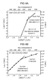
- FIG. 8A is a graph showing an Arrhenius plot of ⁇ obtained by fitting to the time dependence of the ON-state voltage of the field-effect transistor according to the first exemplary embodiment
- FIG. 8B is a graph showing an Arrhenius plot of ⁇ obtained by fitting to the time dependence of the ON-state voltage of Comparative Example;
- FIG. 9 is a graph showing the relationship between the thickness of the undoped GaN layer and the ON-state resistance at switching
- FIG. 10 is a cross-sectional view of a field-effect transistor according to a second embodiment
- FIG. 11 is a cross-sectional view of a conventional field-effect transistor having an AlGaN/GaN heterostructure
- FIG. 12 is a cross-sectional view of a conventional field-effect transistor when turned OFF
- FIG. 13 is a cross-sectional view of a device for evaluating an accelerated life test of a GaN epitaxial film formed on a Si substrate;
- FIG. 14A is a graph showing the leakage current characteristic in a case where a voltage of 600 V is applied to a conventional field-effect device
- FIG. 14B is a graph showing the leakage current characteristic in a case where a voltage of 630 V is applied to the conventional field-effect device
- FIG. 14C is a graph showing the leakage current characteristic in a case where a voltage of 660 V is applied to the conventional field-effect device
- FIG. 14D is a graph showing the leakage current characteristic in a case where a voltage of 700 V is applied to the conventional field-effect device
- FIG. 15 is a graph showing a Weibull plot of the device life when an applied bias voltage is 700 V.
- FIG. 16 is a graph showing the relationship between the device life and initial leakage current.
- the present inventors have found the following problems in the conventional field-effect transistor described in “Description of the Related Art”.
- FIG. 13 is a cross-sectional view of a device for evaluating an accelerated life test of a GaN epitaxial film formed on a Si substrate.
- field-effect device 950 having the layer structure identical to the layer structure of field-effect transistor 900 shown in FIG. 11 , two-dimensional electron gas 960 is formed between separation regions 953 formed by ion injection. Further, Al electrode 958 is formed on epitaxial layer 956 surrounded by separation regions 953 . Threading dislocations of about 10 10 /cm 2 are present at undoped GaN layer 955 formed on a Si substrate 951 . Such dislocations may significantly affect the reliability of the device. Accordingly, the reliability of the epitaxial film was evaluated by an accelerated aging test, which was carried out by applying a voltage to undoped GaN layer 955 on Si substrate 951 in the vertical direction (the thickness direction), and accelerating aging by the temperature.
- FIGS. 14A to 14D are graphs showing the leakage current characteristic in the cases where voltages of 600 V, 630 V, 660 V, and 700 V are applied to the conventional field-effect device, respectively.
- FIGS. 14A to 14D show the relationship at 125° C. between the leakage currents obtained by the above-described evaluation with the applied voltages 600 V to 700 V and the total bias applied time (t 1 +t 2 +t 3 + . . . ). It can be seen that, with any of the applied biases, the leakage current sharply rises at a certain time. Further, it can also be seen that, as the applied biases become higher, the total bias applied time at which the leakage current sharply rises is reached earlier.
- FIG. 15 is a graph showing a Weibull plot of the device life when the applied bias voltage is 700 V.
- the device life is defined by the time when a leakage current of 15 ⁇ A flows.
- the gradient can be represented by just a single type.
- the failure mode is just a single type.
- the m value is 9, i.e., greater than 1.
- the failure type is only the wear-out failure mode.
- FIG. 16 is a graph showing the relationship between the device life and the initial leakage current. There is a strong correlation between the device life and the initial leakage current. The life tends to be longer when the initial leakage current is smaller. From the foregoing, it is very important to suppress the initial leakage current for securing the reliability of the device.
- the current collapse deteriorates as the side effect. Accordingly, in designing the device, it must be intended not only to reduce the leakage current, but also to prevent deterioration of the current collapse.
- Non Patent Literature 2 S. Heikman, S. Keller, S. P. DenBaars, U. K. Mishra, “Growth of Fe doped semi-insulating GaN by metalorganic chemical vapor deposition.” Applied Physics Letters 81 (2002) 439-441
- Non Patent Literature 3 J. B. Webb, H. Tang, S. Rolfe and J. A. Bardwell, “Semi-insulating C-doped GaN and high-mobility AlGaN/GaN heterostructures grown by ammonia molecular beam epitaxy.” Applied Physics Letters 75 (1999) 953-955)).
- carbon (C) is mixed from group III materials in the growth through MOCVD. Since the mixed amount can be controlled by the growth temperature, the growth pressure and the V/III ratio, it is less disadvantageous as compared to introduction of Fe.
- Non Patent Literature 4 discloses a method for raising the resistance of a GaN epitaxial film by, instead of introducing C of high concentration, codoping Si simultaneously with C while suppressing the concentration of C to about 5 ⁇ 10 17 /cm 3 .
- the mechanism of raising the resistance of a GaN epitaxial film by codoping C and Si functions because Si Ga (Si at the Ga position) compensates for C N (C at the N position). Therefore, provided that the resistance can be raised by the codoping, deterioration in crystallinity may be suppressed because the concentration of C can be suppressed as compared to the case where the resistance of GaN is raised solely by C. Further, the reduced concentration of C enables growth at high temperatures. Hence, a reduction in the concentration of V N defects can be expected.
- the GaN layer doped with C and Si and the channel region can be separated from each other by setting the thickness of the upper layer to at least a prescribed value, the leakage current can be reduced while suppressing the occurrence of the current collapse in an OFF state and at an actual operational voltage.
- FIG. 1 is a cross-sectional view of a field-effect transistor according to a first exemplary embodiment.
- field-effect transistor 1 shown in FIG. 1 what are stacked in order on p-type Si substrate 101 are: AlN buffer layer 102 by a thickness of 200 nm; superlattice layer 103 by a thickness of 2 ⁇ m, superlattice layer 103 being made up of 5 nm of AlN and 20 nm of GaN; codoped layer 104 codoped with Si and C by a thickness of 850 nm; undoped GaN layer 105 by a thickness of 500 nm, the concentration of C in undoped GaN layer 105 being set to be equal to or less than 5 ⁇ 10 17 /cm 3 for suppressing the current collapse; and undoped AlGaN layer 106 by a thickness of 50 nm.
- source electrode 107 and drain electrode 109 made of Ti and Al are formed on undoped AlGaN layer 106 .
- source electrode 107 and drain electrode 109 made of Ti and Al are formed.
- two-dimensional electron gas 110 that is present between undoped GaN layer 105 and undoped AlGaN layer 106 is used as a channel.
- Gate electrode 108 is formed between source electrode 107 and drain electrode 109 .
- gate electrode 108 is formed by stacking a p-type AlGaN layer and a p-type GaN layer in order, and thereafter by depositing Pd/Au as an electrode.
- Codoped layer 104 is a first semiconductor layer formed by Al x Ga 1-x N (0 ⁇ x ⁇ 1) being a first nitride semiconductor.
- codoped layer 104 which is formed for reducing leakage is doped with Si as the donor by 1 ⁇ 10 17 /cm 3 and carbon (C) as the acceptor by 5 ⁇ 10 17 /cm 3 .
- C being doped as the acceptor is introduced by auto-doping during the MOCVD growth.
- Si being the donor is intentionally doped.
- the concentration of Si used for compensating for C functioning as the acceptor must not exceed the concentration of C, because GaN becomes conductive when the concentration of Si exceeds the concentration of C. That is, codoped layer 104 contains carbon (C) and Si as the impurity elements. Further, the concentration of C is equal to or higher than 5 ⁇ 10 17 /cm 3 , and the concentration of Si is lower than the concentration of C.
- undoped GaN layer 105 is a second semiconductor layer formed by GaN being a second nitride semiconductor, and the concentration of C in undoped GaN layer 105 is equal to or lower than 1 ⁇ 10 17 /cm 3 .
- a thickness t 105 of undoped GaN layer 105 is equal to or greater than 0.75 ⁇ m.
- Undoped AlGaN layer 106 is formed on undoped GaN layer 105 .
- Undoped AlGaN layer 106 is a third semiconductor layer formed by AlGaN being a third nitride semiconductor with a wider band gap as compared to that of the second nitride semiconductor.
- FIG. 2 is a graph showing the relationship between the concentration of C in the undoped GaN layer and the ON-state resistance at switching. Specifically, the graph of FIG. 2 shows the relationship between the concentration of C in the undoped GaN layer and the ON-state resistance at switching when field-effect transistor 1 is applied with a voltage of 400 V.
- the concentration of C in undoped GaN layer 105 becomes equal to or higher than 1 ⁇ 10 17 /cm 3 , the ON-state resistance at switching disadvantageously rises. Accordingly, the concentration of C in undoped GaN layer 105 must be equal to or less than 1 ⁇ 10 17 /cm 3 .
- concentration of C in codoped layer 104 must be equal to or higher than 5 ⁇ 10 17 /cm 3 .
- FIG. 3 is a graph showing the relationship between the concentration of C in the codoped layer and the epitaxial film breakdown voltage. Note that, the concentration of Si in codoped layer 104 is fixed to 1 ⁇ 10 17 /cm 3 . As a result, it is found that, when the concentration of C is equal to or less than 5 ⁇ 10 17 /cm 3 , a high breakdown voltage cannot be secured. Accordingly, when the layer is codoped also, the concentration of C must be equal to or higher than 5 ⁇ 10 17 /cm 3 .
- field-effect transistor 1 according to the present exemplary embodiment structured as described above and a field-effect transistor according to Comparative Example are compared against each other.
- the field-effect transistor according to Comparative Example is a field-effect transistor including a layer doped solely with C, instead of being codoped with C and Si, so as to raise the resistance.
- the field-effect transistor according to Comparative Example is different from field-effect transistor 1 in that codoped layer 104 is replaced by a doped layer doped with solely C by 1 ⁇ 10 19 /cm 3 . That is, what are stacked in order on p-type Si substrate 101 are: AlN buffer layer 102 by a thickness of 200 nm; superlattice layer 103 made of AlN and GaN layers by a thickness of 2 ⁇ m: a doped layer doped solely with C by 1 ⁇ 10 19 /cm 3 by a thickness of 850 nm; undoped GaN layer 105 by a thickness of 500 nm; and undoped AlGaN layer 106 by a thickness of 50 nm.
- a source electrode, a drain electrode and a gate electrode are similarly structured as field-effect transistor 1 .
- FIG. 4 is a graph showing the relationship between a drain-source leakage current I DS and a drain-source voltage V DS in an OFF state in the field-effect transistor according to the present exemplary embodiment and in Comparative Example.
- the graph of FIG. 4 shows the current-voltage (I DS -V DS ) characteristic at 125° C. and 25° C. when a gate-source voltage V GS is 0 V.
- the leakage current is lower in field-effect transistor 1 according to the present exemplary embodiment in which codoped layer 104 is employed as the buffer layer than in Comparative Example in which no codoped layer is employed. It can be seen that the effect of a reduced leakage current is exhibited by employment of codoped layer 104 .
- FIG. 5 is a schematic diagram of an electric circuit for evaluating the switching characteristic of a device.
- a load resistor R d is connected in series to the drain terminal of a device (the evaluated FET), and an external voltage V dd is applied.
- a gate-source voltage V GS of the evaluated FET is controlled, and the evaluated FET is switched between ON/OFF states.
- the current collapse is discussed. As described above, firstly, when the device is turned OFF, a strong electric field is applied to the region near the 2 DEG, and electrons are trapped in this region. Next, when the device is turned ON, the trapped electrons near the 2 DEG narrow the 2 DEG. Accordingly, the resistance when the device is turned ON (R ON ) rises, whereby the current collapse occurs. Accordingly, by examining in detail the transient response of the ON-state resistance R ON of the device after the device is switched from an OFF state to an ON state, the process of the trapped electrons being discharged can be examined. Additionally, by acquiring the temperature dependence of the discharge process, the trap energy of the electrons can be learned.
- FIG. 6 is a diagram schematically showing the gate-source voltage and the transient response of the ON-state resistance.
- t is the elapsed time from the time point immediately after the evaluated FET transits from an OFF state to an ON state.
- R ON (t) is subjected to fitting by “stretched exponential function” shown in Equation 1.
- R ON ( t ) R DC + ⁇ R e exp( ⁇ ( t / ⁇ ) ⁇ e ) (Equation 1)
- a time constant ⁇ is a relaxation time constant of the ON-state resistance R ON of the evaluated FET in an ON state, and is a time constant of the discharge process of traps that trigger the collapse.
- R DC is R ON when there is no increase in the ON-state resistance due to the collapse
- ⁇ e is an index.
- the foregoing procedure is performed while varying the temperature of the evaluated FET. ⁇ at each temperature is determined, and the determined ⁇ is expressed by an Arrhenius plot. Since ⁇ represents the time constant of discharge of electrons captured in an OFF state of the evaluated FET, the potential energy of the captured electrons can be obtained by expressing the temperature dependence by the Arrhenius plot.
- FIGS. 7A and 7B are graphs showing the time dependence of the ON-state resistance after field-effect transistor 1 according to the first exemplary embodiment and Comparative Example are switched from an OFF state to an ON state, respectively.
- FIGS. 7A and 7B are compared against with each other, the ON-state resistance at switching is great with field-effect transistor 1 according to the present exemplary embodiment. This is because of frequent occurrence of the collapse, and therefore field-effect transistor 1 according to the first exemplary embodiment is measured with the voltage lower than the voltage applied to the Comparative Example.
- FIGS. 8A and 8B are graphs showing Arrhenius plots of ⁇ obtained by fitting to the time dependence of the ON-state voltage of field-effect transistor 1 according to the first exemplary embodiment and Comparative Example, respectively.
- codoped layer 104 includes a first impurity C having an ionization energy Ea (e.g., 0.8 eV) and a concentration Na, and a second impurity Si having an ionization energy Ed (e.g., 0.03 eV) being smaller than the ionization energy Ea, and a concentration Nd being smaller than the concentration Na. Further, codoped layer 104 also involves a trap level whose activation energy (e.g., 2.3 eV) is greater than the sum (e.g., 0.83 eV) of the ionization energy Ea and the ionization energy Ed.
- Ea e.g., 0.8 eV
- a second impurity Si having an ionization energy Ed (e.g., 0.03 eV) being smaller than the ionization energy Ea
- a concentration Nd being smaller than the concentration Na.
- codoped layer 104 also involves a trap level whose activation energy (e.g.
- codoped layer 104 as the buffer layer, the present inventors further considered whether the electron trap having a deep potential energy formed in codoped layer 104 could be prevented from exhibiting the disadvantageous effect when the device is switched ON, by increasing the thickness of undoped GaN layer 105 formed on codoped layer 104 .
- the ON-state resistance when switched at a voltage V dd 400 V, i.e., the voltage used to drive the device, became twice as great as the DC resistance or less than that, achieving the practically usable level.
- variations of the structure of the field-effect transistor shown in FIG. 1 were fabricated in which the thickness (t 105 in the drawing) of the undoped GaN layer formed on codoped layer 104 was varied to 0.5 ⁇ m, 0.75 ⁇ m, 1.0 ⁇ m and 1.25 ⁇ m, and the current collapse was measured.
- FIG. 9 is a graph showing the relationship between the thickness of the undoped GaN layer and the ON-state resistance at switching.
- FIG. 10 is a cross-sectional view of a field-effect transistor according to a second exemplary embodiment.
- field-effect transistor 2 shown in FIG. 10 what are stacked in order on p-type Si substrate 101 are: AlN buffer layer 102 by a thickness of 200 nm; superlattice layer 203 by a thickness of 2 ⁇ m, the superlattice being made up of 5 nm of AlN and 20 nm of GaN and codoped with Si and C; auto-doped layer 204 by a thickness of 0.5 ⁇ m, auto-doped layer 204 containing C by a concentration of 1 ⁇ 10 19 /cm 3 by auto-doping; undoped GaN layer 105 by a thickness of 0.75 ⁇ m, the concentration of C of undoped GaN layer 105 being set to be equal to or less than 1 ⁇ 10 17 /cm 3 for suppressing the current collapse; and undoped AlGaN layer 106 by a thickness of 50 nm.
- Superlattice layer 203 is a first semiconductor layer formed by a superlattice layer structured by Al x Ga 1-x N and Al y Ga 1-y N being a first nitride semiconductor.
- superlattice layer 203 codoped with Si and C for reducing leakage is doped with Si as the donor by 1 ⁇ 10 17 /cm 3 and carbon (C) as the acceptor by 5 ⁇ 10 17 /cm 3 .
- the concentration of Si used for compensating for C functioning as the acceptor must not exceed the concentration of C, because GaN becomes conductive when the concentration of Si exceeds the concentration of C. That is, superlattice layer 203 contains carbon (C) and Si as impurity elements. Further, the concentration of C is equal to or higher than 5 ⁇ 10 17 /cm 3 , and the concentration of Si is lower than the concentration of C.
- undoped GaN layer 105 is a second semiconductor layer formed by GaN being a second nitride semiconductor, and the concentration of C in undoped GaN layer 105 is equal to or lower than 1 ⁇ 10 17 /cm 3 .
- a thickness t 105 of undoped GaN layer 105 is equal to or greater than 0.75 ⁇ m.
- Undoped AlGaN layer 106 is formed on undoped GaN layer 105 .
- Undoped AlGaN layer 106 is a third semiconductor layer formed by AlGaN being a third nitride semiconductor with a band gap wider as compared to that of the second nitride semiconductor.
- the field-effect transistor of the present disclosure is not limited to the above-described exemplary embodiments.
- the present disclosure includes other exemplary embodiments realized by any combination of any constituents in the exemplary embodiments, variations obtained by making any changes which can be devised by a person skilled in the art within the range not deviating from the gist of the present disclosure to the exemplary embodiments, and a variety of devices including the field-effect transistor of the present disclosure.
- a field-effect transistor apparatus obtained by the present disclosure is useful as a power transistor used in a power supply circuit of a consumer appliance such as an air conditioner.
Landscapes
- Junction Field-Effect Transistors (AREA)
Abstract
Description
- NPL 1: S. C. Binari, W. Kruppa, H. B. Dietrich, G. Kelner, A. E. Wickenden and J. A. Freitas Jr., “Fabrication and characterization of GaN FETs” Solid State Electrons 41 (1997) 1549-1554.
R ON(t)=R DC +ΔR eexp(−(t/τ)β
Claims (6)
Applications Claiming Priority (3)
| Application Number | Priority Date | Filing Date | Title |
|---|---|---|---|
| JP2013002543 | 2013-01-10 | ||
| JP2013-002543 | 2013-01-10 | ||
| PCT/JP2013/006450 WO2014108946A1 (en) | 2013-01-10 | 2013-10-31 | Field-effect transistor |
Related Parent Applications (1)
| Application Number | Title | Priority Date | Filing Date |
|---|---|---|---|
| PCT/JP2013/006450 Continuation WO2014108946A1 (en) | 2013-01-10 | 2013-10-31 | Field-effect transistor |
Publications (2)
| Publication Number | Publication Date |
|---|---|
| US20150303293A1 US20150303293A1 (en) | 2015-10-22 |
| US9595606B2 true US9595606B2 (en) | 2017-03-14 |
Family
ID=51166626
Family Applications (1)
| Application Number | Title | Priority Date | Filing Date |
|---|---|---|---|
| US14/790,064 Active US9595606B2 (en) | 2013-01-10 | 2015-07-02 | Field-effect transistor |
Country Status (3)
| Country | Link |
|---|---|
| US (1) | US9595606B2 (en) |
| JP (1) | JPWO2014108946A1 (en) |
| WO (1) | WO2014108946A1 (en) |
Cited By (2)
| Publication number | Priority date | Publication date | Assignee | Title |
|---|---|---|---|---|
| US20150076509A1 (en) * | 2013-09-19 | 2015-03-19 | Fujitsu Limited | Semiconductor device with buffer layer made of nitride semiconductor |
| US11335799B2 (en) * | 2015-03-26 | 2022-05-17 | Chih-Shu Huang | Group-III nitride semiconductor device and method for fabricating the same |
Families Citing this family (17)
| Publication number | Priority date | Publication date | Assignee | Title |
|---|---|---|---|---|
| WO2014108946A1 (en) * | 2013-01-10 | 2014-07-17 | パナソニック株式会社 | Field-effect transistor |
| JP5787417B2 (en) * | 2013-05-14 | 2015-09-30 | コバレントマテリアル株式会社 | Nitride semiconductor substrate |
| JP6398678B2 (en) * | 2014-12-11 | 2018-10-03 | 富士通株式会社 | Semiconductor device and manufacturing method of semiconductor device |
| JP6516483B2 (en) * | 2015-01-22 | 2019-05-22 | 国立大学法人名古屋大学 | Group III nitride semiconductor device and method of manufacturing the same |
| WO2016143265A1 (en) * | 2015-03-11 | 2016-09-15 | パナソニック株式会社 | Nitride semiconductor device |
| JP6570357B2 (en) * | 2015-07-22 | 2019-09-04 | 京セラ株式会社 | Measuring method of current collapse |
| JP6547581B2 (en) * | 2015-10-22 | 2019-07-24 | 三菱電機株式会社 | Semiconductor device |
| JP6708960B2 (en) * | 2016-06-22 | 2020-06-10 | 住友電気工業株式会社 | Nitride semiconductor device and method for manufacturing nitride semiconductor device |
| US9917156B1 (en) * | 2016-09-02 | 2018-03-13 | IQE, plc | Nucleation layer for growth of III-nitride structures |
| JP7108386B2 (en) * | 2017-08-24 | 2022-07-28 | 住友化学株式会社 | Charge trap evaluation method |
| JP6907974B2 (en) * | 2018-03-13 | 2021-07-21 | 株式会社デンソー | Semiconductor device |
| US11031493B2 (en) * | 2018-06-05 | 2021-06-08 | Indian Institute Of Science | Doping and trap profile engineering in GaN buffer to maximize AlGaN/GaN HEMT EPI stack breakdown voltage |
| JP7433014B2 (en) * | 2018-10-30 | 2024-02-19 | ローム株式会社 | semiconductor equipment |
| CN113424326B (en) * | 2019-02-01 | 2024-06-14 | 苏州晶湛半导体有限公司 | A semiconductor structure and a method for preparing the same |
| CN114530491A (en) * | 2020-11-23 | 2022-05-24 | 苏州能讯高能半导体有限公司 | Semiconductor epitaxial structure, preparation method thereof and semiconductor device |
| CN115101585B (en) * | 2022-08-22 | 2022-11-15 | 江西兆驰半导体有限公司 | GaN-based high electron mobility transistor and its preparation method |
| KR20250092830A (en) * | 2023-12-15 | 2025-06-24 | 삼성전자주식회사 | Semiconductor device |
Citations (9)
| Publication number | Priority date | Publication date | Assignee | Title |
|---|---|---|---|---|
| JP2000068498A (en) | 1998-08-21 | 2000-03-03 | Nippon Telegr & Teleph Corp <Ntt> | Insulating nitride film and semiconductor device using the same |
| JP2006114655A (en) | 2004-10-14 | 2006-04-27 | Hitachi Cable Ltd | Semiconductor epitaxial wafer and field effect transistor |
| JP2006332367A (en) | 2005-05-26 | 2006-12-07 | Sumitomo Electric Ind Ltd | High electron mobility transistor, field effect transistor, epitaxial substrate, method for producing epitaxial substrate, and method for producing group III nitride transistor |
| JP2007251144A (en) | 2006-02-20 | 2007-09-27 | Furukawa Electric Co Ltd:The | Semiconductor element |
| US7326971B2 (en) * | 2005-06-08 | 2008-02-05 | Cree, Inc. | Gallium nitride based high-electron mobility devices |
| US20080296619A1 (en) * | 2003-10-07 | 2008-12-04 | Board Of Trustees Of The University Of Illinois | Adhesive bonding with low temperature grown amorphous or polycrystalline compound semiconductors |
| US20120025205A1 (en) | 2010-07-28 | 2012-02-02 | Sumitomo Electric Industries, Ltd. | Semiconductor device |
| US8212288B2 (en) | 2009-09-14 | 2012-07-03 | Covalent Materials Corporation | Compound semiconductor substrate comprising a multilayer buffer layer |
| US20150303293A1 (en) * | 2013-01-10 | 2015-10-22 | Panasonic Intellectual Property Management Co., Ltd. | Field-effect transistor |
-
2013
- 2013-10-31 WO PCT/JP2013/006450 patent/WO2014108946A1/en not_active Ceased
- 2013-10-31 JP JP2014556210A patent/JPWO2014108946A1/en active Pending
-
2015
- 2015-07-02 US US14/790,064 patent/US9595606B2/en active Active
Patent Citations (12)
| Publication number | Priority date | Publication date | Assignee | Title |
|---|---|---|---|---|
| JP2000068498A (en) | 1998-08-21 | 2000-03-03 | Nippon Telegr & Teleph Corp <Ntt> | Insulating nitride film and semiconductor device using the same |
| US20080296619A1 (en) * | 2003-10-07 | 2008-12-04 | Board Of Trustees Of The University Of Illinois | Adhesive bonding with low temperature grown amorphous or polycrystalline compound semiconductors |
| JP2006114655A (en) | 2004-10-14 | 2006-04-27 | Hitachi Cable Ltd | Semiconductor epitaxial wafer and field effect transistor |
| JP2006332367A (en) | 2005-05-26 | 2006-12-07 | Sumitomo Electric Ind Ltd | High electron mobility transistor, field effect transistor, epitaxial substrate, method for producing epitaxial substrate, and method for producing group III nitride transistor |
| US20090189190A1 (en) | 2005-05-26 | 2009-07-30 | Sumitomo Electric Industries, Ltd. | High Electron Mobility Transistor, Field-Effect Transistor, Epitaxial Substrate, Method of Manufacturing Epitaxial Substrate, and Method of Manufacturing Group III Nitride Transistor |
| US20100230723A1 (en) | 2005-05-26 | 2010-09-16 | Sumitomo Electric Industries, Ltd. | High Electron Mobility Transistor, Field-Effect Transistor, and Epitaxial Substrate |
| US7326971B2 (en) * | 2005-06-08 | 2008-02-05 | Cree, Inc. | Gallium nitride based high-electron mobility devices |
| JP2007251144A (en) | 2006-02-20 | 2007-09-27 | Furukawa Electric Co Ltd:The | Semiconductor element |
| US8212288B2 (en) | 2009-09-14 | 2012-07-03 | Covalent Materials Corporation | Compound semiconductor substrate comprising a multilayer buffer layer |
| US20120025205A1 (en) | 2010-07-28 | 2012-02-02 | Sumitomo Electric Industries, Ltd. | Semiconductor device |
| JP2012033575A (en) | 2010-07-28 | 2012-02-16 | Sumitomo Electric Ind Ltd | Semiconductor device |
| US20150303293A1 (en) * | 2013-01-10 | 2015-10-22 | Panasonic Intellectual Property Management Co., Ltd. | Field-effect transistor |
Non-Patent Citations (6)
| Title |
|---|
| C.H.Seager et al., "Role of carbon in GaN", Journal of Applied Physics, vol. 92, No. 11, Dec. 1, 2002 pp. 6553-6560. |
| International Search Report of PCT application No. PCT/JP2013/006450 dated Jan. 28, 2014. |
| Masayuki Fukai Etc: "Role of carbon-related defects to high resistivity mechanism in silicon-doped GaN",2009 IEICE Sougoutaikai, Mar. 17-20, 2009, p. 13, C-6-8, Elekutoronikusu kouen bunsyu2, Matsuyama, Japan; with English translation. |
| Masayuki Fukai Etc:"Characteristics of AlGaN/GaN HFETs with C and Si co-doping high resistivity GaN buffer layer",2011 IEICE Elekutoronikusu sosaethi taikai, Sep. 13-16, 2011, p. 63, C-10-9, Elekutoronikusu kouen ronbunsyu2, Sapporo, Japan; with English translation. |
| Masayuki Fukai Etc:"Effect of C and Si co-doping high resistivity GaN buffer layer on AlGaN/GaN HFETs", Jul. 2011, p. 1-6 , IEICE Technical Report ED2011-37, The Institute of Electronics, Information and Communication Engineers, Japan; with English translation. |
| S.C.Binari et.al., "Fabrication and characterization of GaN FETs", Solid-State Electronics vol. 41, No. 10, pp. 1549-1554, 1997. |
Cited By (2)
| Publication number | Priority date | Publication date | Assignee | Title |
|---|---|---|---|---|
| US20150076509A1 (en) * | 2013-09-19 | 2015-03-19 | Fujitsu Limited | Semiconductor device with buffer layer made of nitride semiconductor |
| US11335799B2 (en) * | 2015-03-26 | 2022-05-17 | Chih-Shu Huang | Group-III nitride semiconductor device and method for fabricating the same |
Also Published As
| Publication number | Publication date |
|---|---|
| WO2014108946A1 (en) | 2014-07-17 |
| US20150303293A1 (en) | 2015-10-22 |
| JPWO2014108946A1 (en) | 2017-01-19 |
Similar Documents
| Publication | Publication Date | Title |
|---|---|---|
| US9595606B2 (en) | Field-effect transistor | |
| JP5649112B2 (en) | Field effect transistor | |
| US7170111B2 (en) | Nitride heterojunction transistors having charge-transfer induced energy barriers and methods of fabricating the same | |
| Simin et al. | SiO/sub 2//AlGaN/InGaN/GaN MOSDHFETs | |
| TWI765974B (en) | Semiconductor substrate, electronic device, semiconductor substrate inspection method and electronic device manufacturing method | |
| CN104704608B (en) | Nitride semiconductor structure | |
| JP5334149B2 (en) | Nitride semiconductor field effect transistor | |
| Wang et al. | Off-state breakdown characterization in AlGaN/GaN HEMT using drain injection technique | |
| US7985984B2 (en) | III-nitride semiconductor field effect transistor | |
| Maeda et al. | Superior pinch-off characteristics at 400 C in AlGaN/GaN heterostructure field effect transistors | |
| Takakura et al. | Low-frequency noise investigation of GaN/AlGaN metal–oxide–semiconductor high-electron-mobility field-effect transistor with different gate length and orientation | |
| US11355626B2 (en) | High electron mobility transistor | |
| US20190103482A1 (en) | Semiconductor power device | |
| US20220199820A1 (en) | Nitride semiconductor device | |
| Rossetto et al. | Performance-limiting traps in GaN-based HEMTs: From native defects to common impurities | |
| US9935192B2 (en) | Optimized buffer layer for high mobility field-effect transistor | |
| US20140183545A1 (en) | Polarization effect carrier generating device structures having compensation doping to reduce leakage current | |
| US8283700B2 (en) | Field effect transistor and manufacturing method thereof | |
| US11316040B2 (en) | High electron mobility transistor | |
| GASKA¹ et al. | AlGaN/GaN high electron mobility transistors | |
| Zhang et al. | Normally-off AlGaN/GaN high electron mobility transistors with thin and high Al composition barrier layers | |
| US20140167081A1 (en) | Semiconductor device | |
| Zhou et al. | Schottky source/drain Al 2 O 3/InAlN/GaN MIS-HEMT with steep sub-threshold swing and high ON/OFF current ratio | |
| Maeda et al. | Two-Dimensional Electron Gas Transport Properties in AlGaN/GaN Heterostructure Field-Effect Transistors | |
| Shivam et al. | High-Performance Analysis of Recessed Gate AlN/β-Ga 2 O 3 HEMT |
Legal Events
| Date | Code | Title | Description |
|---|---|---|---|
| AS | Assignment |
Owner name: PANASONIC INTELLECTUAL PROPERTY MANAGEMENT CO., LT Free format text: ASSIGNMENT OF ASSIGNORS INTEREST;ASSIGNORS:TANAKA, KENICHIRO;KOHDA, SHINICHI;ISHIDA, MASAHIRO;AND OTHERS;SIGNING DATES FROM 20150615 TO 20150616;REEL/FRAME:036116/0839 |
|
| STCF | Information on status: patent grant |
Free format text: PATENTED CASE |
|
| MAFP | Maintenance fee payment |
Free format text: PAYMENT OF MAINTENANCE FEE, 4TH YEAR, LARGE ENTITY (ORIGINAL EVENT CODE: M1551); ENTITY STATUS OF PATENT OWNER: LARGE ENTITY Year of fee payment: 4 |
|
| MAFP | Maintenance fee payment |
Free format text: PAYMENT OF MAINTENANCE FEE, 8TH YEAR, LARGE ENTITY (ORIGINAL EVENT CODE: M1552); ENTITY STATUS OF PATENT OWNER: LARGE ENTITY Year of fee payment: 8 |
|
| AS | Assignment |
Owner name: PANASONIC HOLDINGS CORPORATION, JAPAN Free format text: ASSIGNMENT OF ASSIGNORS INTEREST;ASSIGNOR:PANASONIC INTELLECTUAL PROPERTY MANAGEMENT CO., LTD.;REEL/FRAME:069503/0625 Effective date: 20241120 |
|
| AS | Assignment |
Owner name: PANASONIC HOLDINGS CORPORATION, JAPAN Free format text: ASSIGNMENT OF ASSIGNORS INTEREST;ASSIGNOR:INFINEON TECHNOLOGIES AUSTRIA AG;REEL/FRAME:072853/0508 Effective date: 20250901 |