US9577750B2 - Multifunctional micro sensor system - Google Patents
Multifunctional micro sensor system Download PDFInfo
- Publication number
- US9577750B2 US9577750B2 US14/770,904 US201414770904A US9577750B2 US 9577750 B2 US9577750 B2 US 9577750B2 US 201414770904 A US201414770904 A US 201414770904A US 9577750 B2 US9577750 B2 US 9577750B2
- Authority
- US
- United States
- Prior art keywords
- transmitter
- receiver
- compensation
- signal
- minimum
- Prior art date
- Legal status (The legal status is an assumption and is not a legal conclusion. Google has not performed a legal analysis and makes no representation as to the accuracy of the status listed.)
- Active
Links
Images




Classifications
-
- H—ELECTRICITY
- H04—ELECTRIC COMMUNICATION TECHNIQUE
- H04B—TRANSMISSION
- H04B10/00—Transmission systems employing electromagnetic waves other than radio-waves, e.g. infrared, visible or ultraviolet light, or employing corpuscular radiation, e.g. quantum communication
- H04B10/07—Arrangements for monitoring or testing transmission systems; Arrangements for fault measurement of transmission systems
- H04B10/075—Arrangements for monitoring or testing transmission systems; Arrangements for fault measurement of transmission systems using an in-service signal
- H04B10/079—Arrangements for monitoring or testing transmission systems; Arrangements for fault measurement of transmission systems using an in-service signal using measurements of the data signal
- H04B10/0795—Performance monitoring; Measurement of transmission parameters
-
- G01S17/026—
-
- G—PHYSICS
- G01—MEASURING; TESTING
- G01S—RADIO DIRECTION-FINDING; RADIO NAVIGATION; DETERMINING DISTANCE OR VELOCITY BY USE OF RADIO WAVES; LOCATING OR PRESENCE-DETECTING BY USE OF THE REFLECTION OR RERADIATION OF RADIO WAVES; ANALOGOUS ARRANGEMENTS USING OTHER WAVES
- G01S17/00—Systems using the reflection or reradiation of electromagnetic waves other than radio waves, e.g. lidar systems
- G01S17/02—Systems using the reflection of electromagnetic waves other than radio waves
- G01S17/04—Systems determining the presence of a target
-
- G—PHYSICS
- G01—MEASURING; TESTING
- G01S—RADIO DIRECTION-FINDING; RADIO NAVIGATION; DETERMINING DISTANCE OR VELOCITY BY USE OF RADIO WAVES; LOCATING OR PRESENCE-DETECTING BY USE OF THE REFLECTION OR RERADIATION OF RADIO WAVES; ANALOGOUS ARRANGEMENTS USING OTHER WAVES
- G01S7/00—Details of systems according to groups G01S13/00, G01S15/00, G01S17/00
- G01S7/48—Details of systems according to groups G01S13/00, G01S15/00, G01S17/00 of systems according to group G01S17/00
- G01S7/481—Constructional features, e.g. arrangements of optical elements
- G01S7/4811—Constructional features, e.g. arrangements of optical elements common to transmitter and receiver
- G01S7/4813—Housing arrangements
-
- G—PHYSICS
- G01—MEASURING; TESTING
- G01S—RADIO DIRECTION-FINDING; RADIO NAVIGATION; DETERMINING DISTANCE OR VELOCITY BY USE OF RADIO WAVES; LOCATING OR PRESENCE-DETECTING BY USE OF THE REFLECTION OR RERADIATION OF RADIO WAVES; ANALOGOUS ARRANGEMENTS USING OTHER WAVES
- G01S7/00—Details of systems according to groups G01S13/00, G01S15/00, G01S17/00
- G01S7/48—Details of systems according to groups G01S13/00, G01S15/00, G01S17/00 of systems according to group G01S17/00
- G01S7/481—Constructional features, e.g. arrangements of optical elements
- G01S7/4814—Constructional features, e.g. arrangements of optical elements of transmitters alone
-
- G—PHYSICS
- G01—MEASURING; TESTING
- G01S—RADIO DIRECTION-FINDING; RADIO NAVIGATION; DETERMINING DISTANCE OR VELOCITY BY USE OF RADIO WAVES; LOCATING OR PRESENCE-DETECTING BY USE OF THE REFLECTION OR RERADIATION OF RADIO WAVES; ANALOGOUS ARRANGEMENTS USING OTHER WAVES
- G01S7/00—Details of systems according to groups G01S13/00, G01S15/00, G01S17/00
- G01S7/48—Details of systems according to groups G01S13/00, G01S15/00, G01S17/00 of systems according to group G01S17/00
- G01S7/481—Constructional features, e.g. arrangements of optical elements
- G01S7/4816—Constructional features, e.g. arrangements of optical elements of receivers alone
-
- G—PHYSICS
- G01—MEASURING; TESTING
- G01S—RADIO DIRECTION-FINDING; RADIO NAVIGATION; DETERMINING DISTANCE OR VELOCITY BY USE OF RADIO WAVES; LOCATING OR PRESENCE-DETECTING BY USE OF THE REFLECTION OR RERADIATION OF RADIO WAVES; ANALOGOUS ARRANGEMENTS USING OTHER WAVES
- G01S7/00—Details of systems according to groups G01S13/00, G01S15/00, G01S17/00
- G01S7/48—Details of systems according to groups G01S13/00, G01S15/00, G01S17/00 of systems according to group G01S17/00
- G01S7/497—Means for monitoring or calibrating
Definitions
- sensors are required that are capable to detect the position, the movement and the orientation of hands.
- a generator (G) producing a transmitter signal (S 5 ), through which a transmitter (H) is fed.
- the transmitter (H) transmits into a receiver (D) having passed the transmission path to be measured, which consists of a first partial transmission path (I 1 ) and a second partial transmission path (I 2 ).
- the receiver output signal (S 0 ) of the receiver (D) is converted to a compensation signal (S 3 ) by a controller (CT), through which a compensation transmitter (K) is fed, which transmits typically in a linear superimposing manner into the third transmission path (I 3 ) as well as into the receiver (D).
- CT controller
- the compensation signal (S 3 ) is generated in such a way by the controller (CT) out of the receiver output signal (S 0 ) and the transmitter signal (S 5 ), that the receiver output signal (S 0 ) contains no remaining components of the transmitter signal (S 5 ), with the exception of system noise and a control error.
- HALIOS systems are especially robust towards sources of interference, such as sun light, while simultaneously being robust towards dirt and the drift of a receiver (D).
- One such HALIOS system is for example known from the DE102010014462A1 or the EP2418512A1.
- Halios system If such a Halios system is to be installed into a single SMD housing, there are several challenges to be met, in reference to optics and workability.
- the transmitter (H) the object (O), each within the transmission paths and the receiver (D):
- the light of the transmitter (H) may be transmitted from the transmitter (H) to the object (O) first and from there it may be reflected to the photodiode, the receiver (D). In this way the light of the transmitter (H) should initially be sent from transmitter (H) to object (O), and from there reflected back to the photo diode, the receiver (D). The light of the transmitter (H) should not directly fall on to the photo diode (D). In reference to the light of the compensation transmitter (K) it is the opposite: It should fall directly on the photodiode (D), and if possible not be dispersed onto the object (O).
- a maximum of the transmitted energy should reach the object to be detected, and a maximum of the reflecting light of the object is to be captured by a receiver.
- a lens is proposed which is arranged coaxially to the center point of the transmitter or receiver. (FIG. 3 of DE102012210891A1).
- a problem of the technology disclosed by DE102012210891A1 is that the illumination of the space is significantly lower than that of the device which is part of the invention.
- the lenses reference numbers 218 and 312 of DE102012210891A1 are lowered around a low rim relative to the top cover (reference numbers 219 and 319 of DE102012210891A1). It further limits the illumination.
- the necessary spatial illumination is achieved through a complex three-dimensional arrangement of several sensor modules in accordance with DE102012210891A1 (FIG. 6 of DE102012210891A1).
- the patent application DE102010027499A1 resolves this illumination problem similarly (FIG. 1 of DE102010027499A1) by use of multiple modules corresponding to DE102010027499A1.
- FIG. 1 is a diagram of an exemplary device for measuring an optical transmission path.
- FIG. 2 is a diagram of an exemplary device for measuring an optical transmission path.
- FIG. 3 is a diagram of an exemplary device for measuring an optical transmission path.
- FIG. 4 is a top view of the exemplary device according to FIG. 1 .
- FIG. 5 illustrates an exemplary position of a barrier shown in the top view according to FIG. 4 .
- FIG. 6 illustrates exemplary locations of sensor center points to lens optical axes in the exemplary device according to FIG. 1 .
- FIG. 7 illustrates a cross section of the exemplary device according to FIG. 1 .
- FIG. 8 illustrates a horizontal cut through of the exemplary device according to FIG. 1 .
- FIG. 9 illustrates exemplary orientations of emitted beams from transmitter diodes of the exemplary device according to FIG. 1 .
- FIG. 10 illustrates an exemplary method for generating the exemplary emitted beams of FIG. 8 .
- FIG. 11 illustrates a horizontal cross section of the exemplary device according to FIG. 1 .
- FIG. 12 illustrates a cross section through the compensation transmitter of the exemplary device according to FIG. 1 .
- FIG. 13 illustrates an exemplary optical transmission path between a compensation transmitter and a receiver according in the exemplary device according to FIG. 1 .
- the light of the compensation transmitter within the system is dissipated, so that it does not lead to a situation-dependent basic coupling, like in the state of the art systems, for the other, that the light paths within the systems are perfectly coordinated with each other.
- An electro-optic operating point is run by an electrical operating performance and/or an electrical operating current and/or an electrical operating voltage as the first parameter, which are caused by transmitter (H, 2 , 3 , 4 ) or compensation transmitter (K, 9 ), and the optical effect on the receiver (D) as the second parameter which are generated by a transmitter (H 2 , 3 , 4 ) or compensation transmitter (K, 9 ), operated in this way.
- the transmitter (H) and compensation transmitter (K) are of the same type, preferably from adjacent positions of an LED wafer, to maximize the matching between these LEDs.
- the compensation transmitter (K) here the compensation end diode ( 9 ), is typically found closer to the receiver (D) or the photo diode ( 10 ), it usually radiates significantly brighter into the receiver (D) than the transmitter (H) whose light can only reach the receiver (D) weakened, passing through the transmission paths (I 1 , I 2 ), and through reflection from the object (O) and/or transmission through the object (O).
- the setup of the state of the art for the compensation transmitter (K) and the transmitter (H) forces a different electro-optical operating point in the form of differing electrical energization and/or differing lighting strength of the receiver (D), which ultimately leads to a temperature-dependent test reading.
- FIG. 1 shows an exemplary measurement device.
- the receiver (D) is thereby symbolized by a photo diode with pre-resistor between mass and supply voltage VDD.
- optical barrier (B) marked in FIG. 1 which prevents, that the light of the compensation transmitter (K) and the compensation diode (K) from falling directly on to the object (O).
- the function of that barrier known from EP2418512A1 is as follows: To ensure that the transmitter (H) is able to illuminate the object (O) via the first transmission path (I 1 ), the optical barrier (B) must show an optical transmission path window (WH), which must be transparent for the radiation of the transmitter (H).
- the wave length of the transmitter (H) is referred to as transmitter wave length.
- the barrier (B) is to feature a second optical receiver path window (WD) from the analog ground in the area of the second transmission path (I 2 ), which is transparent for the detectable radiations, and especially for the wave length of the detectable radiation.
- the wave length of the radiations to be detected is typically of the same wave length as the radiation from the transmitter (H), and therefore the transmitter wave length. But this does not necessarily have to be the case. It is for example conceivable, that the object (O) fluoresces under irradiation by the transmitter (H), and that only this fluorescence is to be measured.
- the receiver path window (WD) is typically chosen in such a way, that it would preferably only be transparent for the wave length of the fluorescent radiation, meaning the fluorescence wave length.
- the light of the compensation transmitter (K) is not to escape outward. Therefore it is useful that the receiver path window (WD) and the transmitter path window (WH) are not transparent for the wave length of the light of the compensation transmitter (K), and the compensation transmitter wave length, and it is useful that they absorb light of that wave length. Also, these windows should not to reflect the light of the compensation transmitter (K), so that the light is eliminated from the system, and does not remain inside the system due to multiple reflections, resulting in signal distortions.
- the receiver path window (WD) in front of the detector must be transparent for the wave length of the radiation to be detected, typically the transmitter wave length and/or the fluorescence wave length. It must reliably suppress radiation of the compensation transmitter wave length.
- the compensation transmitter (K) appropriately transmits on a different wave length than the transmitter (H).
- the compensation transmitter wave length should therefore differ from the transmitter wave length.
- the windows are equipped with filters, specifically transmission path filters (FH) for the transmission path and the receiver path filter (FD) for the receiver path, to be able to exemplary fulfill the transmissivity reflectivity.
- transmissivity means the portion of light not damped at a center wave length of the light beam intensity (energy) when passing a filter or a set up component in comparison to the light beam intensity (energy) of the incident light before the passage through the object. For example, in the case of a damping by 50%, the transmissivity is 50%.
- reflectivity means that a portion of light not damped at a center wave length of the light beam intensity (energy) when reflected at a filter or a set up component in comparison to the light beam intensity (energy) of the incident light before the reflection at the object. For example, in the case of a damping by 50% the reflectivity is 50%.
- absorption factor means the degree of light beam intensity (energy) reduction of a light beam at a defined center wave length during reflection at a filter or a package component and parallel transmission through said filter and said package component in comparison to the light beam intensity (energy) of the incident light beam before the reflection at the object. This energy remains in the object and is not reflected and transmitted. For example, with a transmissivity of 25% and a reflectivity of 24% the absorption factor is 50%.
- the transmission path filter (FH) is preferably for the wave length of the transmitter (H), thereby for the transmitter wave length, a transmissivity of ideally 100%, or of at minimum 50%, or at minimum 75%, or at minimum 88%, or at minimum 95%, or at minimum 98%, or at minimum 99%.
- the transmission path filter (FH) is to preferably have a reflectivity of ideally 0%, or at maximum 50%, or at maximum 25%, or at maximum 12%, or at maximum 5%, or at maximum 2%, or at maximum 1% of the transmitter's (H) wave length.
- the transmission path filter (FH) is to preferably have in parallel a transmissivity of ideally 0%, or at maximum 50%, or at maximum 25%, or at maximum 12%, or at maximum 5%, or at maximum 2%, or at maximum 1%.
- the transmission path filter (FH) is to preferably have in parallel an absorption factor of ideally 100%, or at minimum 25%, or at minimum 50%, or at minimum 75%, or at minimum 88%, or at minimum 95%, or at minimum 98%, or at minimum 99%.
- the receiver path filter (FD) is to preferably have a transmissivity of ideally 100%, or at minimum 50%, or at minimum 75%, or at minimum 88%, or at minimum 95%, or at minimum 98% or at minimum 99%.
- the receiver path filter (FD) is to preferably have in parallel a transmissivity of ideally 0%, or at maximum 50%, or at maximum 25%, or at maximum 12%, or at maximum 5%, or at maximum 2%, or at maximum 1%.
- the receiver path filter (FD) is to preferably have in parallel an absorption factor of ideally 100%, or at minimum 25%, or at minimum 50%, or at minimum 75%, or at minimum 88%, or at minimum 95%, or at minimum 98%, or at minimum 99%.
- the light of the transmitter (H) can enter into the device conforming with the principles of the disclosure and thereby to the reach the receiver (D), and at the other hand that the light of the compensation transmitter (K) for one, cannot simultaneously escape from the system, for the other that it can be eliminated from the system as quickly as possible, with as few reflections within the system as possible.
- all materials within the device should be configured for other wave lengths than the following three cases, to have an absorption factor of ideally 100%, or of at minimum 25%, or at minimum 50%, or at minimum 75%, or at minimum 88%, or at minimum 95%, or at minimum 98%, or at minimum 99%.
- the spectral ranges with low absorption factor refer to: first, the wave length of the transmitter (H), therefore the transmitter wave length, second, the wave length of the compensation transmitter (K), therefore the compensation transmitter wave length, and third, the wave length of the radiation to be detected, therefore for example the fluorescence wave length and/or the wave length of the transmitter (H).
- the material of the housing walls is to exhibit an absorption factor of ideally 100%, or at minimum 25%, or at minimum 50%, or at minimum 75%, or at minimum 88%, or at minimum 95%, or at minimum 98%, or at minimum 99% at all wave lengths. Evidently this does not apply for optically transparent parts like lenses, etc.
- a second barrier (B 2 ) as for example known from EP2418512A1 is useful. It prevents this or at least prolongs the optical path or otherwise buffers the unwanted direct signal.
- the compensation transmitter (K) is stored in a compensation transmitter cavity (CAV_K), and therefore surrounded by a third optical barrier (B 3 ). It features a compensation path window (WK), by which the compensation transmitter (K) is able to transmit into the receiver (D), located in its own receiver cavity (CAV_D), through the compensation path window (WK) via a reflector (R).
- the compensation path window (WK) simultaneously fulfills the function of a shield, which prevents the radiation of light from the compensation transmitter (K) into other optical pathways, which might for instance terminate on the object (O). This is of special importance, if the wave length selectivity of the previously discussed filters (FD, FH) is not sufficient.
- the compensation path window (WK) does not solely have the purpose to minimize flare light within the system, but also to minimize the light transferred from the compensation transmitter (K), as far that its intensity in a typical electro-optic operating point approximately aligns, using the same electrical energy supply as that of the transmitter (H), thru the optical transmission paths (I 1 , I 2 ) and the object (O) to the receiver (D).
- Various dimensioning strategies for the compensation path windows (WK) may be considered. Initially it may be considered to size the compensation path window (WK) in such a way, that for a common object (O), for example a hand, at a commonly used spacing, e.g. 25 cm, the electrical operating point of the compensation transmitter (K) and transmitter (H) match.
- the intensity of the radiation of the transmitter (H) is increased by way of preferred control algorithm, and simultaneously the intensity of the compensation transmitter (K) is decreased. In a preferred design of the system this is done to minimize the temperature coefficient of the test reading of the overall system.
- the preferred control parameters are placed into a table, which define by which measure the intensity of the transmitter (H) is to be increased, if the intensity of the transmission intensity of the compensation transmitter (K) is to be decreased, and vice versa.
- FIG. 2 shows the exemplary measurement device in accordance with FIG. 1 , whereby now in contrast to FIG. 1 the transmitter (H) is controlled rather than the compensation transmitter (K).
- FIG. 3 shows the exemplary measurement device in accordance with FIGS. 1 and 2 , whereby in contrast to the systems in FIGS. 1 and 2 the controller (CT) now creates the signal from the now separate generator signal (S 5 G) and the compensation signal (S 3 ).
- This configuration is especially beneficial, if the temperature dependency is to be minimized through the minimizing of the difference between the electric optical working points of compensation transmitter (K) and transmitter (H).
- FIG. 4 shows the exemplary measurement device from an exemplary top view.
- the exemplary device ( 1 ) there are three LEDs ( 2 , 3 , 4 ) used as transmitters (H) and a photo diode ( 9 ) used as a receiver (D).
- a different quantity of receivers (D) and a different quantity of transmitters (H) might be chosen.
- the controller (CT) and potentially also the generator (G) may potentially have to be adjusted.
- the photodiode ( 9 ) receives the light reverberated by the object (O) from transmitters (H) from the LEDs ( 2 , 3 , 4 ).
- the object (O) is not shown in FIG. 4 , and may be understood to be located above the plane of projection in the direction of the observer.
- a preamplifier ( 8 ) is part of the device ( 1 ).
- the compensation transmitter K ( 9 ) is part of the device ( 1 ) as well. All elements ( 2 , 3 , 4 , 10 , 9 , 8 ) are mounted on the upper side of a common lead frame. The electrical connection is made through bonding, preferably by a gold wire bond.
- an edge ( 17 ) is shown, which as the second barrier (B 2 ), optically separates the transmitter diodes ( 2 , 3 , 4 ) from the photo diode ( 10 ), which acts as the receiver (D). Above each of the diodes ( 2 , 3 , 4 ) one lens ( 5 , 6 , 7 ) each is found, which forms the light beams.
- the packaging technology used is that of a molded interconnection device.
- a three-dimensional shaped lead frame is spray-molded with a mold compound.
- MID technology molded interconnection device technology
- An integrated analysis circuit ( 12 ) (IC) is placed on the underside of the MID lead frame, for the activation of the transmitters to drive the transmitters ( 2 , 3 , 4 ), to analyze the receiver (D), here the photo diode ( 10 ), the control of compensation transmitter (K), here the compensation transmitter diode ( 9 ), and the communication with the processor of the operating system (via S 4 ), for example of a cell phone.
- the circuit ( 12 ) thereby typically contains a controller (CT).
- CT controller
- the contacts (e.g. 14 ) of this analysis circuit ( 12 ) are thereby connected with the contacts (e.g. 13 ) of the lead frame thru bonding.
- the analysis circuit ( 12 ) is preferably located in a recess of the housing, so that the bond wires are covered after the pouring of the mold mass.
- the specific shape of the lead frame soldering is still possible on this side of the housing.
- the housing has an optical barrier ( 17 ), which increases a length of the optical path between the transmitters ( 2 , 3 , 4 ) and the receiver (D), here the photodiode ( 10 ), and thereby reduces the coupling across parasitic paths.
- various shapes may be used to form the optical barrier ( 17 ).
- the barrier ( 17 ) may be provided with slightly beveled sides, to ensure that the entire housing can easily be removed from the from the injection mold.
- FIG. 5 shows once again the exemplary position and shape of the barrier ( 17 ) on the upper side of the housing from two different perspectives. Hereby the parasitic optical pathway is lengthened.
- the integrated micro lenses ( 5 , 6 , 7 , 40 ) are placed above the transmitters ( 2 , 3 , 4 ) and the receiver (D), here the photodiode ( 10 ). This is shown in FIG. 6 .
- the lenses ( 5 , 6 , 7 , 40 ) are made of an optically transparent material. Regarding the transparency of these lenses, the implementations of the transmission and reception pathways, the preceding are to be referenced.
- the lenses ( 5 , 6 , 7 , 40 ) direct the emitted light beam ( 36 , 37 , 38 in FIG. 9 ) for an alignment and shape of the respective transmitters ( 2 , 3 , 4 ) in a preferred direction.
- the focal points ( 18 , 20 , 22 ) of the transmitters ( 2 , 3 , 4 ) are offset in relationship to the respective optical axis of the corresponding lens ( 5 , 6 , 7 ).
- the direction of the transmitter beam lobe ( 36 , 37 , 38 ) of the corresponding transmitter diodes ( 2 , 3 , 4 ) changes.
- the size, form, and focal length of the corresponding lens ( 5 , 6 , 7 ) determine the form of the corresponding beam ( 36 , 37 , 38 ).
- Such lenses are for example known from US20050184301A1.
- the lenses ( 5 , 6 , 7 , 40 ) do not need to have cylindrical symmetry.
- the lenses ( 5 , 6 , 7 , 40 ) may be of different shapes. For example, they may be elliptical. Such lenses may have more than two focal lengths.
- the lenses may be manufactured by injection molding of transparent plastic materials. The transparency hereby refers to the wave length of radiation used for transmission and reception.
- lenses ( 40 ) may be used to shape a receiver reception lobe on the receiver side.
- the center points ( 24 ) of the receivers, here the photo diodes ( 10 ) may be offset towards the optical axis ( 25 ) of the corresponding lenses ( 40 ), which is analog to the method of the transmitter beam lobe as described above.
- the center point ( 24 ) and the center of the optical axis ( 25 ) are located on top of each other. As annotated, this does not necessarily have to be the case, depending on the application. It is especially beneficial if the receiver reception lobe/s is/are shaped in such a way, that the coverage ratio between the receiver reception lobes and the transmitter beam lobes is maximized in the relevant area above the sensor. Hereby the sensitivity of the system is maximized, which may improve performance, for example, for motion detection.
- the transmitter beam lobes ( 36 , 37 , 38 ) to be oriented in different directions, for example with three transmitter beam lobes, each rotating by 120° around the axis, turned in perpendicular direction to the top side.
- the transmitter beam lobes overlap a little bit, but such overlap should preferably not exceed 60°.
- a transmitter beam lobe should therefore not be wider than 240°.
- the receiver reception lobe should cover the entire relevant area.
- the relevant lens ( 40 ) of the corresponding receiver (D) photodiode ( 10 )
- the relevant lens ( 40 ) of the corresponding receiver (D) photodiode ( 10 )
- the wave lengths of the transmitter diodes ( 2 , 3 , 4 ) need not to be identical. Colors or wave lengths which are intentionally very different may be chosen for various transmitter diodes ( 2 , 3 , 4 ).
- the receiver (D), here the photodiode ( 10 ), may be sensitive to visible light of all colors and infrared light, and the transmitters ( 2 , 3 , 4 ) consisting of three LEDs in the colors red ( 2 ), blue ( 3 ) and green ( 4 ).
- An infrared LED may in this case be used as the compensation transmitter (D, 9 ).
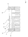
- FIG. 7 shows a transverse section of the exemplary measurement device.
- the lead frame is run in two layers ( 27 , 26 ).
- the components are workable at different heights.
- a wall ( 52 ) surrounds the cavities in which the components ( 2 , 3 , 4 , 8 , 9 , 10 , 12 ) are inserted.
- the photodiode ( 10 ) On the side of the transmitters ( 2 , 3 , 4 , 9 ) and receiver (D), here the photodiode ( 10 ), the transmitter cavity as well as the and the compensation transmitter cavity (CAV_K) are typically filled with a transparent mold compound ( 28 ) with a high refraction index.
- the compensation diode ( 9 ), ( 28 ) is provided with an optical cover ( 51 ) which will be described later.
- FIG. 8 shows a horizontal cross-section of the exemplary measurement device. Shown are various lines ( 29 ), which are part of the MID lead-frame.
- the transmitters ( 2 , 3 , 4 ) are attached to die-paddles ( 32 , 33 , 34 ), typically by gluing or also by soldering. The latter has advantages, if high thermal loads have to be removed.
- the position of barrier ( 17 ) is also shown for better orientation.
- a portion of the lines ( 29 ) lead to contacts ( 11 ) of the device. Internal connections are certainly possible. But, these require a support, which is detached after the mold process.
- the compensation transmitter here the compensation diode ( 9 ) is attached to a suitable die paddle ( 35 ) as well.
- the receiver (D), here the photodiode ( 10 ) is also attached to the corresponding die paddle ( 31 ) and the pre-amplifier ( 8 ) to its die-paddle ( 30 ).
- FIG. 9 shows once again the different exemplary orientations ( 36 , 37 , 38 ) of the transmitter beam lobes of the transmitter diodes ( 2 , 3 , 4 ) of the exemplary measurement device ( 1 ), as well as the corresponding lenses ( 5 , 6 , 7 , 40 ).
- the barrier ( 17 ) is once again shown.
- FIG. 10 depicts how the orientation of the receiver and transmitter beams is performed.
- the transmitter diode to be moved out of its axis by 15°.
- the lens hereby has a diameter of 200 ⁇ m.
- the optical axis of the transmitters ( 18 , 20 , 22 ) or the receiver ( 24 ) respectively are at the height of the transmitters ( 1 , 3 , 4 ) or the receiver (D) (photodiode ( 10 )) offset by a distance (b 1 ) towards the optical axis ( 19 , 21 , 23 , 25 ) of the corresponding lens.
- the light of the transmitter ( 2 , 3 , 4 ) enters the bottom side ( 41 ) of the lens, and is directed by the lens to the direction opposite to the transmitter.
- FIG. 11 shows another horizontal cross-section the exemplary device ( 1 ).
- the recesses ( 16 ) for handling during assembly can be recognized.
- the transmitters ( 2 , 3 , 4 ) are located in separate transmitter cavities ( 53 , 54 , 55 ). These cavities cause an excellent optical decoupling.
- the compensation transmitter (K) also possesses its own compensation transmitter cavity (CAV_K), here cavity ( 57 ) for the compensation diode ( 9 ), which is separated by an optical barrier ( 48 ) from the corresponding receiver cavity (CAV_D), here the cavity ( 56 ) for the photodiode ( 10 ).
- this optical barrier ( 48 ) said third optical barrier (B 3 ) is however modified in its height in such a way, that light is able to pass from the compensation transmitter (K), here the compensation diode ( 9 ), to the receiver (D), meaning the photodiode ( 10 ), as further described below.
- the cavities are optically open to the top side with the exception of the compensation transmitter cavity.
- the cavities appear from the corresponding receiver cavity (CAV_D), here cavity ( 57 ) of the compensation diode ( 9 ) optically open to the top.
- FIG. 12 shows a cross section of an exemplary device ( 1 ) through the compensation transmitter (K), here the compensation diode ( 9 ), and the receiver (D), here the photodiode ( 10 ).
- the receiver (D), here the photodiode ( 10 ) is to be particularly irradiated from its top side and not from its other side by the light of the compensation transmitter (K), here the compensation diode ( 9 ), because the light sensitive layer of the photodiode ( 10 ) is typically located on its surface.
- conforming device ( 1 ) this problem is resolved in such a way, that the compensation transmitter (K), here the compensation diode ( 9 ) transmits light toward the top.
- the opening ( 49 ), the compensation pass window (WK) above the optical barrier ( 48 ) is thereby designed in such a way, that the light transmitted from the compensation transmitter cavity (CAV_K), here cavity ( 57 ) to the receiver cavity (CAV_D), here cavity ( 56 ), preferably solely irradiates the receiver (D), here the photo diode ( 10 ).
- the opening ( 49 ) thereby effectively operates like an optical wave guide.
- the light beam of the compensation diode ( 9 ), thereby of the compensation transmitter (K), is thereby so muted, so that at least at one operating point, which is determined by the reflectivity and distance of a typical object (O), the electrification of the compensation diode ( 9 ), thereby of the compensation transmitter (K), and the electro-optical operating point at minimum of one of the transmitters ( 2 , 3 , 4 ), thereby of a transmitter (H) is the same.
- this transmitter (H, 2 , 3 , 4 ), and said compensation transmitter (K, 9 ) for example are supplied with the identical electric power, and thereby to produce an identical optical effect on the receiver (D).
- the first exemplary possible setting of an unregulated transmitter (H) ( FIG. 1 ) showing here, that this optical operating point is determined through the sensor system, by the smallest geometric gap of the most reflective still recognizable object, e.g. a white object.
- the compensation diode ( 9 ), thereby the compensation transmitter (K) is to be adjusted at a maximum, as the unregulated transmitter ( 2 , 3 , 4 ), thereby of transmitter (H), typically afterwards sends at maximum output.
- the electro-optical operating point of the compensation transmitter (K) is also preferably optimized for the minimal gap of the object (O) with the maximum reflectivity of the same.
- the third setting option there is a typical object (O), for example an object (O) with a maximum reflectivity, at a typical distance, rather than at the minimal distance, measured and the compensation path window (WK), thereby the opening ( 49 ), dimensioned in such a way, that transmitter ( 2 , 3 , 4 ) as well as transmitter (H), as well as the compensation diode ( 9 ), and thereby the compensation transmitter (K), are located in the same electro-optical operating point.
- transmitter ( 2 , 3 , 4 ) as well as transmitter (H), as well as the compensation diode ( 9 ), and thereby the compensation transmitter (K) are located in the same electro-optical operating point.
- transmitter ( 2 , 3 , 4 ) as well as transmitter (H), as well as the compensation diode ( 9 ), and thereby the compensation transmitter (K) are located in the same electro-optical operating point.
- transmitter ( 2 , 3 , 4 ) as well as transmitter (H), as well as the compensation diode (
- the exemplary measurement device is a form of a Halios system for the measuring of an optical transmission path (I 1 , I 2 ), in which the receiver (D, 10 ), and at minimum one compensation transmitter (K, 9 ), which are divided by a minimum of one optical barrier (B 3 , 48 ).
- the receiver (D, 10 ) and at minimum one compensation transmitter (K, 9 ), which are divided by a minimum of one optical barrier (B 3 , 48 ).
- the said optical barrier (B 3 , 48 ) hereby features a compensation pathway to transport the light of the compensation transmitter (K, 9 ) to the receiver (K), of the photodiode ( 10 ).
- This compensation pathway includes a compensation window (WK, 49 ) which muffles the light of said compensation transmitter (K, 9 ).
- the compensation pathway therefor muffles in its entirety the light of compensation transmitter (K), the compensation diode ( 9 ), prior to reaching the receiver (D) in the way, that the compensation transmitter (K, 9 ) and said transmitter (H, 2 , 3 , 4 ) at minimum one optical operating point, e.g. characterized by object reflectivity and object distance by the regulator (CT), operated in the same electro-optical operating point.
- An electro-optical operating point of a transmitter (H) or a compensation transmitter (K) is thereby characterized by two parameters: The first parameter is the light intensity which this transmitter creates at this electro-optical operating point, and thereby the size of the correlating receiver output signal.
- the second parameter is the size of the electrical signal which, for the production of exactly this radiation needs to be run through by the transmitter (H), or compensation transmitter (K), to exactly this transmitter (H) or compensation transmitter (K).
- the setting of the electro-optical operating point is done constructively, in one way by the size of the compensation path window, by the setting of the transparency of the mold compound in the area of the compensation path window, and by the setting of the reflectivity of the wave guide walls in the area of the compensation pathway.
- the transmitting amplitude of the transmitter (H, 2 , 3 , 4 ) and the transmitting amplitude of the compensation transmitter (K, 9 ) with the minimum of one optical operating point, marked by the object distance and object reflectivity is reverse regulated by the regulator (CT).
- the regulation of the typically to be expected range of distance and reflectivity area of typical objects should work reversed, because this way the deviations of the electro-optical operating points of the compensation transmitter (K), thus the compensation transmitter ( 9 ), and the transmitter ( 2 , 3 , 4 , H) are the least.
- the regulation of the sending amplitude of the transmitter (H, 2 , 3 , 4 ) and the regulation of the sending amplitude of the compensation transmitter (K, 9 ) should take place in at minimum one work area, which is also identified by the object distance and object reflectivity, in such a way, that the temperature dependency of the test reading is minimized.
- the material of the housing of the disclosure conforming device ( 1 ) is preferably made of a material which absorbs all radiation in wave length ranges in which the light may escape from the housing, and in all wave length ranges in which the transmitters ( 2 , 3 , 4 , 9 ) are transmitting.
- All housing surfaces should therefore be preferably designed matte, so that the small amount of light, which will be scattered in spite of other measures, will be scattered diffusely. Of course this does not apply to optical surfaces like the upper interface layer of the transparent cover material ( 28 ), where total reflection should occur, and neither to the surfaces of the optical windows (WD, WH) or filters (FD, FH) or lenses ( 5 , 6 , 7 , 40 ).
- angles and shapes of the housing surfaces should thereby be designed in such a way, that multiple reflections preferably do not result in a light path on the receiver (D), here a photodiode ( 10 ).
- This tilting may lead to a reduced sensitivity of the receiver (D), here the photodiode ( 10 ), in regards to the reception of optical radiation, which is reflected back by the object (O). Therefore it continues to be useful to optimize the coupling into the receiver (D), here the photodiode ( 10 ) by way of a diagonal prism, as used for the transmitter (H), here the transmitter diodes ( 2 , 3 , 4 ).
- the receiver (D) and in particular in this case the photodiode ( 10 ), typically made of silicone, may be transparent for a portion of the radiation. In this case it may occur, that a reflection takes place on the underside of the receiver (D), here the photodiode ( 10 ). While this increases the efficiency of the receiver (D), here the photodiode ( 10 ), it ultimately leads to a distortion of the receiver output signal (S 0 ). Therefore it is useful to attach the receiver (D), here the photodiode ( 10 ), to the die paddle ( 31 ) by way of glue, which is absorbent for wave lengths that might pass through the receiver (D), the photodiode ( 10 ).
Landscapes
- Engineering & Computer Science (AREA)
- Physics & Mathematics (AREA)
- Computer Networks & Wireless Communication (AREA)
- General Physics & Mathematics (AREA)
- Radar, Positioning & Navigation (AREA)
- Remote Sensing (AREA)
- Electromagnetism (AREA)
- Signal Processing (AREA)
- Investigating Or Analysing Materials By Optical Means (AREA)
- Optical Communication System (AREA)
Abstract
Description
-
- a. it possesses at minimum one signal generator (G) able to generate at minimum one transmitter signal (S5), driving at minimum one transmitter (H), that irradiates into at minimum one receiver (D) and
- b. it possesses at minimum one controller (CT), which puts out at minimum one compensation signal (S3), by which at minimum one compensation transmitter (K) is driven, which also transmits in a superimposing manner into the at minimum one of the said receivers (D) and
- c. that the said controller (CT) generates the minimum of one said compensation signal (S3), of at minimum one of the receiver output signals (S0) of said receiver (D), and of at minimum one of the said transmitter signal (S5), and
- d. and that the controller (CT) drives the minimum of one compensation transmitter (K) by way of said compensation signal (S3), that said receiver output signal (S0) of said receiver (D) contains no remaining components of the transmitter signal (S5) except for a control error and system noise.
or in the second version - e. it possesses a minimum of one signal generator (G), capable of producing the minimum of compensation signal (S3), by which the minimum of one compensation transmitter (K) is controlled, which at minimum transmits into one receiver (D) and
- f. it possesses the minimum of one controller (CT) emitting the minimum of one transmitter signal (S5) which drives the minimum one transmitter (H), which also transmits in a superimposing manner into the at minimum one receiver (D), and
- g. that said controller (CT) generates the at minimum one of said transmitter signal (S5) out of a minimum of a receiver output signal (S0) of one of the said receivers (D) and at minimum one compensation transmitter signal (S3), and
- h. and that the controller (CT) drives a minimum one transmitter (H) by way of a minimum of one said transmitter signal (S5) in such a way that the receiver output signal (S0) of said receiver (D) contains no remaining components of the compensation transmitter signal (S3) except for a control error and system noise
or - i. that it is a combination of the first and second version
and
- ii. that at minimum of said optical transmitters (H) it is able to transmit at minimum into a first transmission path (I1) which is only a partial component of the device, and
- iii. which terminates at minimum one object (O), which is not part of the device, located at the end of the first transmission path (I1), and able to transmit light into at minimum of a second transmission path (I2), which is only a partial component of the device, and which terminates at minimum one of the said receivers (D), which is part of the device, and
- iv. that at minimum one of these receivers (D), which is able to receive the transmitter signal (S5) modified by the transmission through the first transmission path (I1) and/or the second transmission path (I2) and/or the reflection by the object (O) and to transform the transmitter signal (S5) at minimum into one receiver output signal (S0) and
- v. that one of said controllers (CT), which is part of the device, outputs the minimum of one signal (S4), which may be used outside the device and
- vi. that this signal (S4) represents the measure of a minimum of one feature, at minimum of one first transmission path (I1) or one second transmission path, or representative reading at minimum for one property at minimum for one object (O) at the end of one of the said first transmission paths (I1) or at the beginning of said second transmission path (I2), and over an output signal (S4) at minimum, emitted upon request and
- vii. that this compensation transmitter (K) transmits into at minimum one third transmission path (I3), which is entirely a component of the device and
- viii. that at minimum one of the third transmission paths (I3) terminates at the minimum by one said receiver (D) and
- ix. that at minimum this receiver (D) is capable of picking up at minimum the signal in said compensation transmitter (K), superimposed with the signal at minimum by one transmitter (H)
Claims (20)
Applications Claiming Priority (10)
| Application Number | Priority Date | Filing Date | Title |
|---|---|---|---|
| DE102013003791.3 | 2013-02-27 | ||
| DE102013003791 | 2013-02-27 | ||
| DE102013003791 | 2013-02-27 | ||
| DE102013005787 | 2013-03-28 | ||
| DE102013005787.6 | 2013-03-28 | ||
| DE102013005787 | 2013-03-28 | ||
| WOPCT/DE2014/000024 | 2014-01-22 | ||
| PCT/DE2014/000024 WO2014131385A1 (en) | 2013-02-27 | 2014-01-22 | Multifunctional optical micro sensor system |
| DEPCT/DE2014/000024 | 2014-01-22 | ||
| PCT/DE2014/000046 WO2014131386A1 (en) | 2013-02-27 | 2014-02-07 | Multifunctional optical micro sensor system |
Publications (2)
| Publication Number | Publication Date |
|---|---|
| US20160006505A1 US20160006505A1 (en) | 2016-01-07 |
| US9577750B2 true US9577750B2 (en) | 2017-02-21 |
Family
ID=49304634
Family Applications (2)
| Application Number | Title | Priority Date | Filing Date |
|---|---|---|---|
| US14/384,217 Active US9300397B2 (en) | 2013-02-27 | 2014-01-22 | Multifunctional optical micro sensor system |
| US14/770,904 Active US9577750B2 (en) | 2013-02-27 | 2014-02-07 | Multifunctional micro sensor system |
Family Applications Before (1)
| Application Number | Title | Priority Date | Filing Date |
|---|---|---|---|
| US14/384,217 Active US9300397B2 (en) | 2013-02-27 | 2014-01-22 | Multifunctional optical micro sensor system |
Country Status (2)
| Country | Link |
|---|---|
| US (2) | US9300397B2 (en) |
| WO (1) | WO2014131386A1 (en) |
Families Citing this family (1)
| Publication number | Priority date | Publication date | Assignee | Title |
|---|---|---|---|---|
| EP3803445B1 (en) * | 2018-05-25 | 2025-09-10 | Ams Ag | Filter for reducing optical cross-talk |
Citations (15)
| Publication number | Priority date | Publication date | Assignee | Title |
|---|---|---|---|---|
| US20030155487A1 (en) * | 2000-03-19 | 2003-08-21 | Gerd Reime | Method and device for opto-electronically determining the position of an object |
| DE10256429A1 (en) | 2002-12-02 | 2004-06-24 | Gerd Reime | Method and arrangement for measuring a modulated light signal |
| US20050184301A1 (en) | 2004-02-25 | 2005-08-25 | Sharp Kabushiki Kaisha | Multiple ranging apparatus |
| DE102006003269A1 (en) | 2006-01-24 | 2007-07-26 | Mechaless Systems Gmbh | Light duration measuring method, involves mixing multiple clock signals of two clock controls in mixer for forming mixed signal, and utilizing phase shift between mixed signal and filter signal for determining light duration |
| DE102006020570A1 (en) | 2006-05-01 | 2007-11-08 | Mechaless Systems Gmbh | Optoelectronic device for detecting the position and / or movement of an object and associated method |
| DE102010014462A1 (en) | 2010-04-09 | 2011-10-13 | Ecomal Deutschland Gmbh | Control device for driving an electrical load and method for operating such a control device |
| DE102010028967A1 (en) | 2010-04-26 | 2011-10-27 | Balluff Gmbh | Optical sensor device |
| DE102010027499A1 (en) | 2010-07-16 | 2012-01-19 | Mechaless Systems Gmbh | Optical control, in particular push-button or switch |
| WO2012013757A1 (en) | 2010-07-30 | 2012-02-02 | Mechaless Systems Gmbh | Opto-electronic measuring arrangement with electro-optical basic coupling |
| DE102012102056A1 (en) | 2011-04-27 | 2012-10-31 | Leuze Electronic Gmbh & Co. Kg | Optical sensor for detecting objects in monitored area, has transmitted light beam emitting transmitter and receiver which is formed for receiving transmitted light beam that is reflected as received light beam from object |
| EP2549652A2 (en) | 2011-07-18 | 2013-01-23 | Hysonic. Co., Ltd. | Motion sensing switch |
| DE102012210891A1 (en) | 2011-07-26 | 2013-01-31 | Avago Technologies Ecbu Ip (Singapore) Pte. Ltd. | Multi-directional proximity sensor |
| WO2013134456A1 (en) | 2012-03-09 | 2013-09-12 | Halliburton Energy Services, Inc. | Set-delayed cement compositions comprising pumice and associated methods |
| US20140341567A1 (en) * | 2012-02-03 | 2014-11-20 | Mechaless Systems Gmbh | Compensation for an optical sensor via a printed circuit board |
| US20160077208A1 (en) * | 2013-04-17 | 2016-03-17 | Mechaless Systems Gmbh | Method for optically measuring distances in the near and far range |
Family Cites Families (10)
| Publication number | Priority date | Publication date | Assignee | Title |
|---|---|---|---|---|
| CA2352680C (en) * | 2000-07-07 | 2006-01-10 | Nippon Telegraph And Telephone Corporation | Multi-wavelength generating method and apparatus based on flattening of optical spectrum |
| JP4301822B2 (en) * | 2003-01-24 | 2009-07-22 | 富士通株式会社 | Optical amplifier with polarization mode dispersion compensation function |
| US7580639B2 (en) * | 2003-12-29 | 2009-08-25 | Verizon Business Global Llc | Characterization and control of optical dispersion compensating element |
| US7061596B2 (en) * | 2004-08-19 | 2006-06-13 | Lucent Technologies Inc. | Wavelength-tracking dispersion compensator |
| US8787771B2 (en) * | 2006-10-06 | 2014-07-22 | Ciena Corporation | All-optical regenerator and optical network incorporating same |
| JP5736837B2 (en) * | 2011-02-23 | 2015-06-17 | 富士通株式会社 | Optical receiver |
| GB2498336A (en) * | 2012-01-04 | 2013-07-17 | Oclaro Technology Plc | Monitoring multiple optical channels |
| DE102012201650A1 (en) | 2012-02-03 | 2013-08-08 | Sgl Carbon Se | Heat shield with outer fiber winding |
| EP2631674A1 (en) | 2012-02-23 | 2013-08-28 | ELMOS Semiconductor AG | Method and sensor system for measuring the properties of a transfer segment of a measuring system between transmitter and recipient |
| US9002150B2 (en) * | 2012-05-08 | 2015-04-07 | General Dynamics Advanced Information Systems, Inc. | Optical sensing system and method |
-
2014
- 2014-01-22 US US14/384,217 patent/US9300397B2/en active Active
- 2014-02-07 US US14/770,904 patent/US9577750B2/en active Active
- 2014-02-07 WO PCT/DE2014/000046 patent/WO2014131386A1/en not_active Ceased
Patent Citations (20)
| Publication number | Priority date | Publication date | Assignee | Title |
|---|---|---|---|---|
| US20030155487A1 (en) * | 2000-03-19 | 2003-08-21 | Gerd Reime | Method and device for opto-electronically determining the position of an object |
| DE10256429A1 (en) | 2002-12-02 | 2004-06-24 | Gerd Reime | Method and arrangement for measuring a modulated light signal |
| US20050184301A1 (en) | 2004-02-25 | 2005-08-25 | Sharp Kabushiki Kaisha | Multiple ranging apparatus |
| DE102006003269A1 (en) | 2006-01-24 | 2007-07-26 | Mechaless Systems Gmbh | Light duration measuring method, involves mixing multiple clock signals of two clock controls in mixer for forming mixed signal, and utilizing phase shift between mixed signal and filter signal for determining light duration |
| DE102006020570A1 (en) | 2006-05-01 | 2007-11-08 | Mechaless Systems Gmbh | Optoelectronic device for detecting the position and / or movement of an object and associated method |
| DE102010014462A1 (en) | 2010-04-09 | 2011-10-13 | Ecomal Deutschland Gmbh | Control device for driving an electrical load and method for operating such a control device |
| DE102010028967A1 (en) | 2010-04-26 | 2011-10-27 | Balluff Gmbh | Optical sensor device |
| DE102010027499A1 (en) | 2010-07-16 | 2012-01-19 | Mechaless Systems Gmbh | Optical control, in particular push-button or switch |
| CN103154769A (en) | 2010-07-30 | 2013-06-12 | 梅卡雷斯系统有限责任公司 | Opto-electronic measuring arrangement with electro-optical basic coupling |
| EP2418512A1 (en) | 2010-07-30 | 2012-02-15 | Mechaless Systems GmbH | Optoelectronic measuring assembly with compensation for external light sources |
| KR20130052741A (en) | 2010-07-30 | 2013-05-23 | 메카레스 시스템스 게엠베하 | Opto-electronic measuring arrangement with electro-optical basic coupling |
| EP2598908A1 (en) | 2010-07-30 | 2013-06-05 | Mechaless Systems GmbH | Opto-electronic measuring arrangement with electro-optical basic coupling |
| WO2012013757A1 (en) | 2010-07-30 | 2012-02-02 | Mechaless Systems Gmbh | Opto-electronic measuring arrangement with electro-optical basic coupling |
| US20130181613A1 (en) | 2010-07-30 | 2013-07-18 | Mechaless Systems Gmbh | Opto-electronic measuring arrangement with electro-optical basic coupling |
| DE102012102056A1 (en) | 2011-04-27 | 2012-10-31 | Leuze Electronic Gmbh & Co. Kg | Optical sensor for detecting objects in monitored area, has transmitted light beam emitting transmitter and receiver which is formed for receiving transmitted light beam that is reflected as received light beam from object |
| EP2549652A2 (en) | 2011-07-18 | 2013-01-23 | Hysonic. Co., Ltd. | Motion sensing switch |
| DE102012210891A1 (en) | 2011-07-26 | 2013-01-31 | Avago Technologies Ecbu Ip (Singapore) Pte. Ltd. | Multi-directional proximity sensor |
| US20140341567A1 (en) * | 2012-02-03 | 2014-11-20 | Mechaless Systems Gmbh | Compensation for an optical sensor via a printed circuit board |
| WO2013134456A1 (en) | 2012-03-09 | 2013-09-12 | Halliburton Energy Services, Inc. | Set-delayed cement compositions comprising pumice and associated methods |
| US20160077208A1 (en) * | 2013-04-17 | 2016-03-17 | Mechaless Systems Gmbh | Method for optically measuring distances in the near and far range |
Non-Patent Citations (1)
| Title |
|---|
| International Search Report for PCT/DE2014/000046 dated May 15, 2014 (10 pages; with English translation). |
Also Published As
| Publication number | Publication date |
|---|---|
| US20160006505A1 (en) | 2016-01-07 |
| US20150110485A1 (en) | 2015-04-23 |
| WO2014131386A1 (en) | 2014-09-04 |
| US9300397B2 (en) | 2016-03-29 |
Similar Documents
| Publication | Publication Date | Title |
|---|---|---|
| CN109814086B (en) | a lidar | |
| CN114341600B (en) | Optical measurement equipment including internal spectral reference | |
| JP7312979B2 (en) | Laser transceiver module and its optical adjustment method, laser radar and automatic driving device | |
| US10393874B2 (en) | Distance measuring device | |
| KR102235710B1 (en) | Scanning lidar having optical structures with transmission receiving single lens | |
| JP4991787B2 (en) | Reflective photoelectric sensor | |
| JP6046475B2 (en) | Improved transistor outline (TO) -CAN assembly for use in optical communications | |
| KR20230126704A (en) | LiDAR system using transmit optical power monitor | |
| CN108594206A (en) | Light delivery module, laser emitting module, laser radar system and vehicle | |
| JP2018028555A (en) | Device and method for rotating lidar platform with shared transmission/light-reception path | |
| KR102263183B1 (en) | Lidar device | |
| KR101581061B1 (en) | Light barrier and method for detecting objects | |
| US11226402B2 (en) | Optical ranging systems including optical cross-talk reducing features | |
| US9297750B2 (en) | Methods and apparatus for an optical system outputting direct light and having a sensor | |
| US11550054B2 (en) | Optical triangulation sensor for distance measurement | |
| US10692912B2 (en) | Optical device for exposure of a sensor device for a vehicle | |
| US20160006505A1 (en) | Multifunctional micro sensor system | |
| CN103940740B (en) | For detecting the sensor device of the humidity on panel | |
| JP2012220353A (en) | Gas component detection apparatus | |
| WO2022252309A1 (en) | Ranging device, lidar, and mobile robot | |
| WO2021033391A1 (en) | Protective cover and light-emitting device | |
| US8876327B2 (en) | Laser light source module and method of manufacturing laser light source module | |
| WO2014131385A1 (en) | Multifunctional optical micro sensor system | |
| JP2016523415A (en) | Photodetection module and manufacturing method thereof | |
| CN118519124A (en) | Laser packaging structure, laser radar transmitting device and laser radar system |
Legal Events
| Date | Code | Title | Description |
|---|---|---|---|
| AS | Assignment |
Owner name: ELMOS SEMICONDUCTOR AG, GERMANY Free format text: ASSIGNMENT OF ASSIGNORS INTEREST;ASSIGNORS:HASE, MICHAEL;DOMOKOS, MICHAEL;HILL, UWE HENDRIK;REEL/FRAME:036438/0172 Effective date: 20150811 |
|
| STCF | Information on status: patent grant |
Free format text: PATENTED CASE |
|
| MAFP | Maintenance fee payment |
Free format text: PAYMENT OF MAINTENANCE FEE, 4TH YEAR, LARGE ENTITY (ORIGINAL EVENT CODE: M1551); ENTITY STATUS OF PATENT OWNER: LARGE ENTITY Year of fee payment: 4 |
|
| AS | Assignment |
Owner name: ELMOS SEMICONDUCTOR SE, GERMANY Free format text: CHANGE OF NAME;ASSIGNOR:ELMOS SEMICONDUCTOR AKTIENGESELLSCHAFT;REEL/FRAME:053608/0986 Effective date: 20200824 |
|
| MAFP | Maintenance fee payment |
Free format text: PAYMENT OF MAINTENANCE FEE, 8TH YEAR, LARGE ENTITY (ORIGINAL EVENT CODE: M1552); ENTITY STATUS OF PATENT OWNER: LARGE ENTITY Year of fee payment: 8 |
|
| AS | Assignment |
Owner name: ELMOS SEMICONDUCTOR SE, GERMANY Free format text: CHANGE OF ADDRESS;ASSIGNOR:ELMOS SEMICONDUCTOR SE;REEL/FRAME:074852/0964 Effective date: 20250630 |