US9564596B2 - Heterocyclic compound and organic light-emitting device comprising same - Google Patents
Heterocyclic compound and organic light-emitting device comprising same Download PDFInfo
- Publication number
- US9564596B2 US9564596B2 US14/243,800 US201414243800A US9564596B2 US 9564596 B2 US9564596 B2 US 9564596B2 US 201414243800 A US201414243800 A US 201414243800A US 9564596 B2 US9564596 B2 US 9564596B2
- Authority
- US
- United States
- Prior art keywords
- group
- compound
- unsubstituted
- substituted
- formula
- Prior art date
- Legal status (The legal status is an assumption and is not a legal conclusion. Google has not performed a legal analysis and makes no representation as to the accuracy of the status listed.)
- Active, expires
Links
- 150000002391 heterocyclic compounds Chemical class 0.000 title description 2
- 150000001875 compounds Chemical class 0.000 claims abstract description 117
- 239000010410 layer Substances 0.000 claims description 53
- 239000000463 material Substances 0.000 claims description 49
- 239000012044 organic layer Substances 0.000 claims description 35
- 239000002346 layers by function Substances 0.000 claims description 28
- 125000004093 cyano group Chemical group *C#N 0.000 claims description 25
- 125000004435 hydrogen atom Chemical group [H]* 0.000 claims description 22
- 239000002019 doping agent Substances 0.000 claims description 21
- MWPLVEDNUUSJAV-UHFFFAOYSA-N anthracene Chemical compound C1=CC=CC2=CC3=CC=CC=C3C=C21 MWPLVEDNUUSJAV-UHFFFAOYSA-N 0.000 claims description 18
- 229910052805 deuterium Inorganic materials 0.000 claims description 18
- 125000004431 deuterium atom Chemical group 0.000 claims description 18
- 125000005843 halogen group Chemical group 0.000 claims description 16
- 125000000449 nitro group Chemical group [O-][N+](*)=O 0.000 claims description 16
- 125000003367 polycyclic group Chemical group 0.000 claims description 15
- 125000002887 hydroxy group Chemical group [H]O* 0.000 claims description 13
- 125000006743 (C1-C60) alkyl group Chemical group 0.000 claims description 12
- 125000006749 (C6-C60) aryl group Chemical group 0.000 claims description 11
- 125000001072 heteroaryl group Chemical group 0.000 claims description 10
- 238000002347 injection Methods 0.000 claims description 10
- 239000007924 injection Substances 0.000 claims description 10
- 239000010409 thin film Substances 0.000 claims description 8
- 125000003837 (C1-C20) alkyl group Chemical group 0.000 claims description 7
- 125000006736 (C6-C20) aryl group Chemical group 0.000 claims description 6
- 125000003178 carboxy group Chemical group [H]OC(*)=O 0.000 claims description 6
- 230000005525 hole transport Effects 0.000 claims description 6
- 125000003342 alkenyl group Chemical group 0.000 claims description 4
- 150000004696 coordination complex Chemical class 0.000 claims description 4
- 229910044991 metal oxide Inorganic materials 0.000 claims description 4
- 150000004706 metal oxides Chemical class 0.000 claims description 4
- 125000000732 arylene group Chemical group 0.000 claims description 3
- 125000005549 heteroarylene group Chemical group 0.000 claims description 3
- 125000005647 linker group Chemical group 0.000 claims description 3
- 150000004059 quinone derivatives Chemical group 0.000 claims description 3
- 150000004982 aromatic amines Chemical class 0.000 claims description 2
- 238000000034 method Methods 0.000 claims description 2
- 125000005504 styryl group Chemical group 0.000 claims description 2
- 230000015572 biosynthetic process Effects 0.000 description 76
- 238000003786 synthesis reaction Methods 0.000 description 72
- 239000011541 reaction mixture Substances 0.000 description 45
- 229940125904 compound 1 Drugs 0.000 description 29
- OKKJLVBELUTLKV-UHFFFAOYSA-N Methanol Chemical compound OC OKKJLVBELUTLKV-UHFFFAOYSA-N 0.000 description 24
- YMWUJEATGCHHMB-UHFFFAOYSA-N Dichloromethane Chemical compound ClCCl YMWUJEATGCHHMB-UHFFFAOYSA-N 0.000 description 23
- 150000003839 salts Chemical class 0.000 description 21
- CSNNHWWHGAXBCP-UHFFFAOYSA-L Magnesium sulfate Chemical compound [Mg+2].[O-][S+2]([O-])([O-])[O-] CSNNHWWHGAXBCP-UHFFFAOYSA-L 0.000 description 20
- 238000000151 deposition Methods 0.000 description 20
- 238000004895 liquid chromatography mass spectrometry Methods 0.000 description 20
- 230000008021 deposition Effects 0.000 description 19
- -1 methoxy, ethoxy, propoxy, isopropyloxy, butoxy Chemical group 0.000 description 19
- 0 CC#N.CC#N.[1*:0]C1=C([11*:0])C([19*])=C([18*])C2=C(C3=C4C([17*])=C([16*])C([15*])=C([14*])C4=C([13*])C([12*])=C3[11*])C3=C(C([2*:0])=C([3*:0])C([4*:0])=C3[5*:0])C(CC)=C12.[1*:0]C1=C([21*:0])C([29*])=C([28*])C2=C(C3=C4C([27*])=C([26*])C([25*])=C([24*])C4=C([23*])C([22*])=C3[21*])C([3*:0])=C([2*:0])C(CC)=C12.[10*:0]N1C2=CC=CC3=C2C2=C1C=CC=C2C=C3.[20*:0]N1C2=CC=CC3=C2C2=C1C=CC=C2C=C3 Chemical compound CC#N.CC#N.[1*:0]C1=C([11*:0])C([19*])=C([18*])C2=C(C3=C4C([17*])=C([16*])C([15*])=C([14*])C4=C([13*])C([12*])=C3[11*])C3=C(C([2*:0])=C([3*:0])C([4*:0])=C3[5*:0])C(CC)=C12.[1*:0]C1=C([21*:0])C([29*])=C([28*])C2=C(C3=C4C([27*])=C([26*])C([25*])=C([24*])C4=C([23*])C([22*])=C3[21*])C([3*:0])=C([2*:0])C(CC)=C12.[10*:0]N1C2=CC=CC3=C2C2=C1C=CC=C2C=C3.[20*:0]N1C2=CC=CC3=C2C2=C1C=CC=C2C=C3 0.000 description 18
- 125000001424 substituent group Chemical group 0.000 description 18
- OAKJQQAXSVQMHS-UHFFFAOYSA-N Hydrazine Chemical compound NN OAKJQQAXSVQMHS-UHFFFAOYSA-N 0.000 description 16
- 238000005160 1H NMR spectroscopy Methods 0.000 description 14
- MYKQKWIPLZEVOW-UHFFFAOYSA-N 11h-benzo[a]carbazole Chemical group C1=CC2=CC=CC=C2C2=C1C1=CC=CC=C1N2 MYKQKWIPLZEVOW-UHFFFAOYSA-N 0.000 description 13
- 239000011248 coating agent Substances 0.000 description 13
- 238000000576 coating method Methods 0.000 description 13
- 239000002904 solvent Substances 0.000 description 13
- XLYOFNOQVPJJNP-UHFFFAOYSA-N water Substances O XLYOFNOQVPJJNP-UHFFFAOYSA-N 0.000 description 13
- XEKOWRVHYACXOJ-UHFFFAOYSA-N Ethyl acetate Chemical compound CCOC(C)=O XEKOWRVHYACXOJ-UHFFFAOYSA-N 0.000 description 12
- 125000001997 phenyl group Chemical group [H]C1=C([H])C([H])=C(*)C([H])=C1[H] 0.000 description 12
- 125000001624 naphthyl group Chemical group 0.000 description 11
- 238000004528 spin coating Methods 0.000 description 11
- 239000000758 substrate Substances 0.000 description 11
- 238000001771 vacuum deposition Methods 0.000 description 11
- NBIIXXVUZAFLBC-UHFFFAOYSA-N Phosphoric acid Chemical group OP(O)(O)=O NBIIXXVUZAFLBC-UHFFFAOYSA-N 0.000 description 10
- 238000000605 extraction Methods 0.000 description 10
- 229910052943 magnesium sulfate Inorganic materials 0.000 description 10
- 235000019341 magnesium sulphate Nutrition 0.000 description 10
- 125000005428 anthryl group Chemical group [H]C1=C([H])C([H])=C2C([H])=C3C(*)=C([H])C([H])=C([H])C3=C([H])C2=C1[H] 0.000 description 9
- 238000010898 silica gel chromatography Methods 0.000 description 9
- PCLIMKBDDGJMGD-UHFFFAOYSA-N N-bromosuccinimide Chemical compound BrN1C(=O)CCC1=O PCLIMKBDDGJMGD-UHFFFAOYSA-N 0.000 description 8
- 239000000872 buffer Substances 0.000 description 8
- 230000000052 comparative effect Effects 0.000 description 8
- 239000013078 crystal Substances 0.000 description 8
- BWHMMNNQKKPAPP-UHFFFAOYSA-L potassium carbonate Chemical compound [K+].[K+].[O-]C([O-])=O BWHMMNNQKKPAPP-UHFFFAOYSA-L 0.000 description 8
- 125000000008 (C1-C10) alkyl group Chemical group 0.000 description 7
- KKHFRAFPESRGGD-UHFFFAOYSA-N 1,3-dimethyl-7-[3-(n-methylanilino)propyl]purine-2,6-dione Chemical compound C1=NC=2N(C)C(=O)N(C)C(=O)C=2N1CCCN(C)C1=CC=CC=C1 KKHFRAFPESRGGD-UHFFFAOYSA-N 0.000 description 7
- MUBZPKHOEPUJKR-UHFFFAOYSA-N Oxalic acid Chemical group OC(=O)C(O)=O MUBZPKHOEPUJKR-UHFFFAOYSA-N 0.000 description 7
- 125000000217 alkyl group Chemical group 0.000 description 7
- 125000003277 amino group Chemical group 0.000 description 7
- 125000003739 carbamimidoyl group Chemical group C(N)(=N)* 0.000 description 7
- 125000003983 fluorenyl group Chemical group C1(=CC=CC=2C3=CC=CC=C3CC12)* 0.000 description 7
- 150000007857 hydrazones Chemical class 0.000 description 7
- AICOOMRHRUFYCM-ZRRPKQBOSA-N oxazine, 1 Chemical compound C([C@@H]1[C@H](C(C[C@]2(C)[C@@H]([C@H](C)N(C)C)[C@H](O)C[C@]21C)=O)CC1=CC2)C[C@H]1[C@@]1(C)[C@H]2N=C(C(C)C)OC1 AICOOMRHRUFYCM-ZRRPKQBOSA-N 0.000 description 7
- 125000000542 sulfonic acid group Chemical group 0.000 description 7
- RFFLAFLAYFXFSW-UHFFFAOYSA-N 1,2-dichlorobenzene Chemical compound ClC1=CC=CC=C1Cl RFFLAFLAYFXFSW-UHFFFAOYSA-N 0.000 description 6
- PSLUFJFHTBIXMW-WYEYVKMPSA-N [(3r,4ar,5s,6s,6as,10s,10ar,10bs)-3-ethenyl-10,10b-dihydroxy-3,4a,7,7,10a-pentamethyl-1-oxo-6-(2-pyridin-2-ylethylcarbamoyloxy)-5,6,6a,8,9,10-hexahydro-2h-benzo[f]chromen-5-yl] acetate Chemical compound O([C@@H]1[C@@H]([C@]2(O[C@](C)(CC(=O)[C@]2(O)[C@@]2(C)[C@@H](O)CCC(C)(C)[C@@H]21)C=C)C)OC(=O)C)C(=O)NCCC1=CC=CC=N1 PSLUFJFHTBIXMW-WYEYVKMPSA-N 0.000 description 6
- 125000003118 aryl group Chemical group 0.000 description 6
- 230000000903 blocking effect Effects 0.000 description 6
- QARVLSVVCXYDNA-UHFFFAOYSA-N bromobenzene Chemical compound BrC1=CC=CC=C1 QARVLSVVCXYDNA-UHFFFAOYSA-N 0.000 description 6
- 125000001725 pyrenyl group Chemical group 0.000 description 6
- VVCMGAUPZIKYTH-VGHSCWAPSA-N 2-acetyloxybenzoic acid;[(2s,3r)-4-(dimethylamino)-3-methyl-1,2-diphenylbutan-2-yl] propanoate;1,3,7-trimethylpurine-2,6-dione Chemical compound CC(=O)OC1=CC=CC=C1C(O)=O.CN1C(=O)N(C)C(=O)C2=C1N=CN2C.C([C@](OC(=O)CC)([C@H](C)CN(C)C)C=1C=CC=CC=1)C1=CC=CC=C1 VVCMGAUPZIKYTH-VGHSCWAPSA-N 0.000 description 5
- OPFJDXRVMFKJJO-ZHHKINOHSA-N N-{[3-(2-benzamido-4-methyl-1,3-thiazol-5-yl)-pyrazol-5-yl]carbonyl}-G-dR-G-dD-dD-dD-NH2 Chemical compound S1C(C=2NN=C(C=2)C(=O)NCC(=O)N[C@H](CCCN=C(N)N)C(=O)NCC(=O)N[C@H](CC(O)=O)C(=O)N[C@H](CC(O)=O)C(=O)N[C@H](CC(O)=O)C(N)=O)=C(C)N=C1NC(=O)C1=CC=CC=C1 OPFJDXRVMFKJJO-ZHHKINOHSA-N 0.000 description 5
- 229940126086 compound 21 Drugs 0.000 description 5
- 125000000027 (C1-C10) alkoxy group Chemical group 0.000 description 4
- 125000006744 (C2-C60) alkenyl group Chemical group 0.000 description 4
- 125000006745 (C2-C60) alkynyl group Chemical group 0.000 description 4
- YSUIQYOGTINQIN-UZFYAQMZSA-N 2-amino-9-[(1S,6R,8R,9S,10R,15R,17R,18R)-8-(6-aminopurin-9-yl)-9,18-difluoro-3,12-dihydroxy-3,12-bis(sulfanylidene)-2,4,7,11,13,16-hexaoxa-3lambda5,12lambda5-diphosphatricyclo[13.2.1.06,10]octadecan-17-yl]-1H-purin-6-one Chemical compound NC1=NC2=C(N=CN2[C@@H]2O[C@@H]3COP(S)(=O)O[C@@H]4[C@@H](COP(S)(=O)O[C@@H]2[C@@H]3F)O[C@H]([C@H]4F)N2C=NC3=C2N=CN=C3N)C(=O)N1 YSUIQYOGTINQIN-UZFYAQMZSA-N 0.000 description 4
- HZMCBFYBIMINFR-UHFFFAOYSA-N 4,4,5,5-tetramethyl-2-(10-naphthalen-1-ylanthracen-9-yl)-1,3,2-dioxaborolane Chemical compound O1C(C)(C)C(C)(C)OB1C(C1=CC=CC=C11)=C(C=CC=C2)C2=C1C1=CC=CC2=CC=CC=C12 HZMCBFYBIMINFR-UHFFFAOYSA-N 0.000 description 4
- MINMDCMSHDBHKG-UHFFFAOYSA-N 4-[4-[[6-methoxy-2-(2-methoxyimidazo[2,1-b][1,3,4]thiadiazol-6-yl)-1-benzofuran-4-yl]oxymethyl]-5-methyl-1,3-thiazol-2-yl]morpholine Chemical compound N1=C2SC(OC)=NN2C=C1C(OC1=CC(OC)=C2)=CC1=C2OCC(=C(S1)C)N=C1N1CCOCC1 MINMDCMSHDBHKG-UHFFFAOYSA-N 0.000 description 4
- WYFCZWSWFGJODV-MIANJLSGSA-N 4-[[(1s)-2-[(e)-3-[3-chloro-2-fluoro-6-(tetrazol-1-yl)phenyl]prop-2-enoyl]-5-(4-methyl-2-oxopiperazin-1-yl)-3,4-dihydro-1h-isoquinoline-1-carbonyl]amino]benzoic acid Chemical compound O=C1CN(C)CCN1C1=CC=CC2=C1CCN(C(=O)\C=C\C=1C(=CC=C(Cl)C=1F)N1N=NN=C1)[C@@H]2C(=O)NC1=CC=C(C(O)=O)C=C1 WYFCZWSWFGJODV-MIANJLSGSA-N 0.000 description 4
- OJRUSAPKCPIVBY-KQYNXXCUSA-N C1=NC2=C(N=C(N=C2N1[C@H]3[C@@H]([C@@H]([C@H](O3)COP(=O)(CP(=O)(O)O)O)O)O)I)N Chemical compound C1=NC2=C(N=C(N=C2N1[C@H]3[C@@H]([C@@H]([C@H](O3)COP(=O)(CP(=O)(O)O)O)O)O)I)N OJRUSAPKCPIVBY-KQYNXXCUSA-N 0.000 description 4
- 239000011575 calcium Substances 0.000 description 4
- 238000005266 casting Methods 0.000 description 4
- 229940125758 compound 15 Drugs 0.000 description 4
- 239000011521 glass Substances 0.000 description 4
- 239000011777 magnesium Substances 0.000 description 4
- 238000004519 manufacturing process Methods 0.000 description 4
- 229910052751 metal Inorganic materials 0.000 description 4
- 239000002184 metal Substances 0.000 description 4
- 229920000767 polyaniline Polymers 0.000 description 4
- 229910000027 potassium carbonate Inorganic materials 0.000 description 4
- 125000006746 (C1-C60) alkoxy group Chemical group 0.000 description 3
- NYPYPOZNGOXYSU-UHFFFAOYSA-N 3-bromopyridine Chemical compound BrC1=CC=CN=C1 NYPYPOZNGOXYSU-UHFFFAOYSA-N 0.000 description 3
- WEVYAHXRMPXWCK-UHFFFAOYSA-N Acetonitrile Chemical compound CC#N WEVYAHXRMPXWCK-UHFFFAOYSA-N 0.000 description 3
- IAZDPXIOMUYVGZ-UHFFFAOYSA-N Dimethylsulphoxide Chemical compound CS(C)=O IAZDPXIOMUYVGZ-UHFFFAOYSA-N 0.000 description 3
- KFZMGEQAYNKOFK-UHFFFAOYSA-N Isopropanol Chemical compound CC(C)O KFZMGEQAYNKOFK-UHFFFAOYSA-N 0.000 description 3
- YXFVVABEGXRONW-UHFFFAOYSA-N Toluene Chemical compound CC1=CC=CC=C1 YXFVVABEGXRONW-UHFFFAOYSA-N 0.000 description 3
- 229910052782 aluminium Inorganic materials 0.000 description 3
- XAGFODPZIPBFFR-UHFFFAOYSA-N aluminium Chemical compound [Al] XAGFODPZIPBFFR-UHFFFAOYSA-N 0.000 description 3
- 229910000147 aluminium phosphate Inorganic materials 0.000 description 3
- 125000006267 biphenyl group Chemical group 0.000 description 3
- 229940125898 compound 5 Drugs 0.000 description 3
- 125000001495 ethyl group Chemical group [H]C([H])([H])C([H])([H])* 0.000 description 3
- 239000011159 matrix material Substances 0.000 description 3
- 125000002496 methyl group Chemical group [H]C([H])([H])* 0.000 description 3
- IBHBKWKFFTZAHE-UHFFFAOYSA-N n-[4-[4-(n-naphthalen-1-ylanilino)phenyl]phenyl]-n-phenylnaphthalen-1-amine Chemical compound C1=CC=CC=C1N(C=1C2=CC=CC=C2C=CC=1)C1=CC=C(C=2C=CC(=CC=2)N(C=2C=CC=CC=2)C=2C3=CC=CC=C3C=CC=2)C=C1 IBHBKWKFFTZAHE-UHFFFAOYSA-N 0.000 description 3
- QIQXTHQIDYTFRH-UHFFFAOYSA-N octadecanoic acid Chemical compound CCCCCCCCCCCCCCCCCC(O)=O QIQXTHQIDYTFRH-UHFFFAOYSA-N 0.000 description 3
- 150000002894 organic compounds Chemical class 0.000 description 3
- 125000001792 phenanthrenyl group Chemical group C1(=CC=CC=2C3=CC=CC=C3C=CC12)* 0.000 description 3
- 229920003227 poly(N-vinyl carbazole) Polymers 0.000 description 3
- 125000001436 propyl group Chemical group [H]C([*])([H])C([H])([H])C([H])([H])[H] 0.000 description 3
- 125000004076 pyridyl group Chemical group 0.000 description 3
- XOLBLPGZBRYERU-UHFFFAOYSA-N tin dioxide Chemical compound O=[Sn]=O XOLBLPGZBRYERU-UHFFFAOYSA-N 0.000 description 3
- 125000006818 (C3-C60) cycloalkyl group Chemical group 0.000 description 2
- 125000006761 (C6-C60) arylene group Chemical group 0.000 description 2
- 125000006751 (C6-C60) aryloxy group Chemical group 0.000 description 2
- 125000006752 (C6-C60) arylthio group Chemical group 0.000 description 2
- DLKQHBOKULLWDQ-UHFFFAOYSA-N 1-bromonaphthalene Chemical compound C1=CC=C2C(Br)=CC=CC2=C1 DLKQHBOKULLWDQ-UHFFFAOYSA-N 0.000 description 2
- HZNVUJQVZSTENZ-UHFFFAOYSA-N 2,3-dichloro-5,6-dicyano-1,4-benzoquinone Chemical compound ClC1=C(Cl)C(=O)C(C#N)=C(C#N)C1=O HZNVUJQVZSTENZ-UHFFFAOYSA-N 0.000 description 2
- GEQBRULPNIVQPP-UHFFFAOYSA-N 2-[3,5-bis(1-phenylbenzimidazol-2-yl)phenyl]-1-phenylbenzimidazole Chemical compound C1=CC=CC=C1N1C2=CC=CC=C2N=C1C1=CC(C=2N(C3=CC=CC=C3N=2)C=2C=CC=CC=2)=CC(C=2N(C3=CC=CC=C3N=2)C=2C=CC=CC=2)=C1 GEQBRULPNIVQPP-UHFFFAOYSA-N 0.000 description 2
- VQGHOUODWALEFC-UHFFFAOYSA-N 2-phenylpyridine Chemical compound C1=CC=CC=C1C1=CC=CC=N1 VQGHOUODWALEFC-UHFFFAOYSA-N 0.000 description 2
- OBAJPWYDYFEBTF-UHFFFAOYSA-N 2-tert-butyl-9,10-dinaphthalen-2-ylanthracene Chemical compound C1=CC=CC2=CC(C3=C4C=CC=CC4=C(C=4C=C5C=CC=CC5=CC=4)C4=CC=C(C=C43)C(C)(C)C)=CC=C21 OBAJPWYDYFEBTF-UHFFFAOYSA-N 0.000 description 2
- AWXGSYPUMWKTBR-UHFFFAOYSA-N 4-carbazol-9-yl-n,n-bis(4-carbazol-9-ylphenyl)aniline Chemical compound C12=CC=CC=C2C2=CC=CC=C2N1C1=CC=C(N(C=2C=CC(=CC=2)N2C3=CC=CC=C3C3=CC=CC=C32)C=2C=CC(=CC=2)N2C3=CC=CC=C3C3=CC=CC=C32)C=C1 AWXGSYPUMWKTBR-UHFFFAOYSA-N 0.000 description 2
- XXPBFNVKTVJZKF-UHFFFAOYSA-N 9,10-dihydrophenanthrene Chemical compound C1=CC=C2CCC3=CC=CC=C3C2=C1 XXPBFNVKTVJZKF-UHFFFAOYSA-N 0.000 description 2
- VIZUPBYFLORCRA-UHFFFAOYSA-N 9,10-dinaphthalen-2-ylanthracene Chemical compound C12=CC=CC=C2C(C2=CC3=CC=CC=C3C=C2)=C(C=CC=C2)C2=C1C1=CC=C(C=CC=C2)C2=C1 VIZUPBYFLORCRA-UHFFFAOYSA-N 0.000 description 2
- VFUDMQLBKNMONU-UHFFFAOYSA-N 9-[4-(4-carbazol-9-ylphenyl)phenyl]carbazole Chemical group C12=CC=CC=C2C2=CC=CC=C2N1C1=CC=C(C=2C=CC(=CC=2)N2C3=CC=CC=C3C3=CC=CC=C32)C=C1 VFUDMQLBKNMONU-UHFFFAOYSA-N 0.000 description 2
- CSCPPACGZOOCGX-UHFFFAOYSA-N Acetone Chemical compound CC(C)=O CSCPPACGZOOCGX-UHFFFAOYSA-N 0.000 description 2
- 229910001148 Al-Li alloy Inorganic materials 0.000 description 2
- VHUUQVKOLVNVRT-UHFFFAOYSA-N Ammonium hydroxide Chemical compound [NH4+].[OH-] VHUUQVKOLVNVRT-UHFFFAOYSA-N 0.000 description 2
- OYPRJOBELJOOCE-UHFFFAOYSA-N Calcium Chemical compound [Ca] OYPRJOBELJOOCE-UHFFFAOYSA-N 0.000 description 2
- RYGMFSIKBFXOCR-UHFFFAOYSA-N Copper Chemical compound [Cu] RYGMFSIKBFXOCR-UHFFFAOYSA-N 0.000 description 2
- LFQSCWFLJHTTHZ-UHFFFAOYSA-N Ethanol Chemical compound CCO LFQSCWFLJHTTHZ-UHFFFAOYSA-N 0.000 description 2
- UEXCJVNBTNXOEH-UHFFFAOYSA-N Ethynylbenzene Chemical group C#CC1=CC=CC=C1 UEXCJVNBTNXOEH-UHFFFAOYSA-N 0.000 description 2
- 101000837344 Homo sapiens T-cell leukemia translocation-altered gene protein Proteins 0.000 description 2
- FYYHWMGAXLPEAU-UHFFFAOYSA-N Magnesium Chemical compound [Mg] FYYHWMGAXLPEAU-UHFFFAOYSA-N 0.000 description 2
- HZONTHOQCHOCTB-UHFFFAOYSA-N N#CC1=CC2=C3C(=C1)N(C1=C4C=CC=CC4=CC=C1)C1=C3C(=C(C3=C4C=CC=CC4=C(C4=CC=CC5=C4C=CC=C5)C4=C3C=CC=C4)C=C1)/C=C\2.N#CC1=CC2=C3C(=C1)N(C1=CC=C4C=CC=CC4=C1)C1=C3C(=C(C3=C4C=CC=CC4=C(C4=CC=CC5=C4C=CC=C5)C4=C3C=CC=C4)C=C1)/C=C\2.N#CC1=CC2=C3C(=C1)N(C1=CC=C4C=CC=CC4=N1)C1=C3C(=C(C3=CC=C(C4=C5C=CC=CC5=C(C5=CC=CC6=C5C=CC=C6)C5=C4C=CC=C5)C=C3)C=C1)/C=C\2.N#CC1=CC2=C3C(=C1)N(C1=CC=CC4=C1C=CC=C4)C1=C3C(=C(C3=C4C=CC=CC4=C(C4=CC=C(C5=CC=CN=C5)C5=C4C=CC=C5)C4=C3C=CC=C4)C=C1)/C=C\2.N#CC1=CC2=C3C(=C1)N(C1=CC=CC=C1)C1=C3C(=C(C3=C4C=CC=CC4=C(C4=CC=C(C5=CC=CC=C5)C5=C4C=CC=C5)C4=C3C=CC=C4)C=C1)/C=C\2.N#CC1=CC2=C3C(=C1)N(C1=CC=CC=C1)C1=C3C(=C(C3=C4C=CC=CC4=C(C4=CC=C(C5=CC=CN=C5)C5=C4C=CC=C5)C4=C3C=CC=C4)C=C1)/C=C\2.N#CC1=CC2=C3C(=C1)N(C1=CC=CC=C1)C1=C3C(=C(C3=CC=C(C4=C5C=CC=CC5=C(C5=CC=CC6=C5C=CC=C6)C5=C4C=CC=C5)C=C3)C=C1)/C=C\2.N#CC1=CC2=C3C(=C1)N(C1=CN=CC=C1)C1=C3C(=C(C3=C4C=CC=CC4=C(C4=C5C=CC=CC5=C(C5=CC=CC6=C5C=CC=C6)C5=C4C=CC=C5)C=C3)C=C1)/C=C\2 Chemical compound N#CC1=CC2=C3C(=C1)N(C1=C4C=CC=CC4=CC=C1)C1=C3C(=C(C3=C4C=CC=CC4=C(C4=CC=CC5=C4C=CC=C5)C4=C3C=CC=C4)C=C1)/C=C\2.N#CC1=CC2=C3C(=C1)N(C1=CC=C4C=CC=CC4=C1)C1=C3C(=C(C3=C4C=CC=CC4=C(C4=CC=CC5=C4C=CC=C5)C4=C3C=CC=C4)C=C1)/C=C\2.N#CC1=CC2=C3C(=C1)N(C1=CC=C4C=CC=CC4=N1)C1=C3C(=C(C3=CC=C(C4=C5C=CC=CC5=C(C5=CC=CC6=C5C=CC=C6)C5=C4C=CC=C5)C=C3)C=C1)/C=C\2.N#CC1=CC2=C3C(=C1)N(C1=CC=CC4=C1C=CC=C4)C1=C3C(=C(C3=C4C=CC=CC4=C(C4=CC=C(C5=CC=CN=C5)C5=C4C=CC=C5)C4=C3C=CC=C4)C=C1)/C=C\2.N#CC1=CC2=C3C(=C1)N(C1=CC=CC=C1)C1=C3C(=C(C3=C4C=CC=CC4=C(C4=CC=C(C5=CC=CC=C5)C5=C4C=CC=C5)C4=C3C=CC=C4)C=C1)/C=C\2.N#CC1=CC2=C3C(=C1)N(C1=CC=CC=C1)C1=C3C(=C(C3=C4C=CC=CC4=C(C4=CC=C(C5=CC=CN=C5)C5=C4C=CC=C5)C4=C3C=CC=C4)C=C1)/C=C\2.N#CC1=CC2=C3C(=C1)N(C1=CC=CC=C1)C1=C3C(=C(C3=CC=C(C4=C5C=CC=CC5=C(C5=CC=CC6=C5C=CC=C6)C5=C4C=CC=C5)C=C3)C=C1)/C=C\2.N#CC1=CC2=C3C(=C1)N(C1=CN=CC=C1)C1=C3C(=C(C3=C4C=CC=CC4=C(C4=C5C=CC=CC5=C(C5=CC=CC6=C5C=CC=C6)C5=C4C=CC=C5)C=C3)C=C1)/C=C\2 HZONTHOQCHOCTB-UHFFFAOYSA-N 0.000 description 2
- VEAHHFVFZJROHE-UHFFFAOYSA-N N#CC1=CC2=C3C(=C1)N(C1=C4C=CC=CC4=CC=C1)C1=C3C(=C(C3=C4C=CC=CC4=C(C4=CC=CC5=C4C=CC=C5)C=C3)C=C1)/C=C\2.N#CC1=CC2=C3C(=C1)N(C1=CC=C4C=CC=CC4=C1)C1=C3C(=C(C3=C4C=CC=CC4=C(C4=CC=CC5=C4C=CC=C5)C=C3)C=C1)/C=C\2.N#CC1=CC2=C3C(=C1)N(C1=CC=CC4=C1C=CC=C4)C1=C3C(=C(C3=C4C=CC=CC4=C(C4=CC=C(C5=CC=CN=C5)C5=C4C=CC=C5)C=C3)C=C1)/C=C\2.N#CC1=CC2=C3C(=C1)N(C1=CC=CC=C1)C1=C3C(=C(C3=C4C=CC=CC4=C(C4=CC=C(C5=CC=CC=C5)C5=C4C=CC=C5)C=C3)C=C1)/C=C\2.N#CC1=CC2=C3C(=C1)N(C1=CC=CC=C1)C1=C3C(=C(C3=C4C=CC=CC4=C(C4=CC=C(C5=CC=CN=C5)C5=C4C=CC=C5)C=C3)C=C1)/C=C\2.N#CC1=CC2=C3C(=C1)N(C1=CC=CC=C1)C1=C3C(=C(C3=C4C=CC=CC4=C(C4=CC=CC5=C4C=CC=C5)C=C3)C=C1)/C=C\2.[C-]#[N+]C1=CC=C(C2=C3C=CC=CC3=C(C3=C4/C=C\C5=C6C(=CC=C5[N+]#[C-])N(C5=CC=CC=C5)C(=C46)C=C3)C=C2)C2=C1C=CC=C2.[C-]#[N+]C1=CC=C(C2=CC=C(C3=C4C=CC=CC4=C(C4=C5/C=C\C6=C7C(=CC=C6[N+]#[C-])N(C6=CC=CC=C6)C(=C57)C=C4)C=C3)C3=C2C=CC=C3)C=C1.[C-]#[N+]C1=CC=C2C3=C1/C=C\C1=C(C4=C5C=CC=CC5=C(C5=CC=C(C6=CC=CC=C6)C6=C5C=CC=C6)C=C4)C=CC(=C13)N2C1=CC=CC=C1.[C-]#[N+]C1=CC=C2C3=C1/C=C\C1=C(C4=CC=C(C5=C6C=CC=CC6=C(C6=CC=CC7=C6C=CC=C7)C=C5)C=C4)C=CC(=C13)N2C1=CC=CC=C1 Chemical compound N#CC1=CC2=C3C(=C1)N(C1=C4C=CC=CC4=CC=C1)C1=C3C(=C(C3=C4C=CC=CC4=C(C4=CC=CC5=C4C=CC=C5)C=C3)C=C1)/C=C\2.N#CC1=CC2=C3C(=C1)N(C1=CC=C4C=CC=CC4=C1)C1=C3C(=C(C3=C4C=CC=CC4=C(C4=CC=CC5=C4C=CC=C5)C=C3)C=C1)/C=C\2.N#CC1=CC2=C3C(=C1)N(C1=CC=CC4=C1C=CC=C4)C1=C3C(=C(C3=C4C=CC=CC4=C(C4=CC=C(C5=CC=CN=C5)C5=C4C=CC=C5)C=C3)C=C1)/C=C\2.N#CC1=CC2=C3C(=C1)N(C1=CC=CC=C1)C1=C3C(=C(C3=C4C=CC=CC4=C(C4=CC=C(C5=CC=CC=C5)C5=C4C=CC=C5)C=C3)C=C1)/C=C\2.N#CC1=CC2=C3C(=C1)N(C1=CC=CC=C1)C1=C3C(=C(C3=C4C=CC=CC4=C(C4=CC=C(C5=CC=CN=C5)C5=C4C=CC=C5)C=C3)C=C1)/C=C\2.N#CC1=CC2=C3C(=C1)N(C1=CC=CC=C1)C1=C3C(=C(C3=C4C=CC=CC4=C(C4=CC=CC5=C4C=CC=C5)C=C3)C=C1)/C=C\2.[C-]#[N+]C1=CC=C(C2=C3C=CC=CC3=C(C3=C4/C=C\C5=C6C(=CC=C5[N+]#[C-])N(C5=CC=CC=C5)C(=C46)C=C3)C=C2)C2=C1C=CC=C2.[C-]#[N+]C1=CC=C(C2=CC=C(C3=C4C=CC=CC4=C(C4=C5/C=C\C6=C7C(=CC=C6[N+]#[C-])N(C6=CC=CC=C6)C(=C57)C=C4)C=C3)C3=C2C=CC=C3)C=C1.[C-]#[N+]C1=CC=C2C3=C1/C=C\C1=C(C4=C5C=CC=CC5=C(C5=CC=C(C6=CC=CC=C6)C6=C5C=CC=C6)C=C4)C=CC(=C13)N2C1=CC=CC=C1.[C-]#[N+]C1=CC=C2C3=C1/C=C\C1=C(C4=CC=C(C5=C6C=CC=CC6=C(C6=CC=CC7=C6C=CC=C7)C=C5)C=C4)C=CC(=C13)N2C1=CC=CC=C1 VEAHHFVFZJROHE-UHFFFAOYSA-N 0.000 description 2
- BOFMTVJJPHTTGN-UHFFFAOYSA-N N#CC1=CC2=C3C(=C1)N(C1=C4C=CC=CC4=CC=C1)C1=CC(C4=C5C=CC=CC5=C(C5=CC=C(C6=CC=CC=C6)C6=C5C=CC=C6)C5=C4C=CC=C5)=CC(=C13)/C=C\2.N#CC1=CC2=C3C(=C1)N(C1=CC=CC=C1)C1=CC(C4=CC=C(C5=C6C=CC=CC6=C(C6=CC=CC7=C6C=CC=C7)C6=C5C=CC=C6)C=C4)=CC(=C13)/C=C\2.N#CC1=CC2=C3C(=C1)N(C1=CC=CC=C1)C1=CC(C4=NC=C(C5=C6C=CC=CC6=C(C6=CC=CC7=C6C=CC=C7)C6=C5C=CC=C6)C=C4)=CC(=C13)/C=C\2.N#CC1=CC2=C3C(=C1)N(C1=CN=CC=C1)C1=CC(C4=C5C=CC=CC5=C(C5=CC=CC6=C5C=CC=C6)C5=C4C=CC=C5)=CC(=C13)/C=C\2.[C-]#[N+]C1=CC=C2C3=C1/C=C\C1=C(C4=C5C=CC=CC5=C(C5=CC=C(C6=CC=C7C8=C6/C=C\C6=C8C(=CC=C6C#N)N7C6=CC=CC=C6)C6=C5C=CC=C6)C5=C4C=CC=C5)C=CC(=C13)N2C1=CC=CC=C1.[C-]#[N+]C1=CC=C2C3=C1/C=C\C1=C(C4=C5C=CC=CC5=C(C5=CC=C(C6=CC=C7C8=C6/C=C\C6=C8C(=CC=C6C#N)N7C6=CN=CC=C6)C6=C5C=CC=C6)C5=C4C=CC=C5)C=CC(=C13)N2C1=CC=CN=C1 Chemical compound N#CC1=CC2=C3C(=C1)N(C1=C4C=CC=CC4=CC=C1)C1=CC(C4=C5C=CC=CC5=C(C5=CC=C(C6=CC=CC=C6)C6=C5C=CC=C6)C5=C4C=CC=C5)=CC(=C13)/C=C\2.N#CC1=CC2=C3C(=C1)N(C1=CC=CC=C1)C1=CC(C4=CC=C(C5=C6C=CC=CC6=C(C6=CC=CC7=C6C=CC=C7)C6=C5C=CC=C6)C=C4)=CC(=C13)/C=C\2.N#CC1=CC2=C3C(=C1)N(C1=CC=CC=C1)C1=CC(C4=NC=C(C5=C6C=CC=CC6=C(C6=CC=CC7=C6C=CC=C7)C6=C5C=CC=C6)C=C4)=CC(=C13)/C=C\2.N#CC1=CC2=C3C(=C1)N(C1=CN=CC=C1)C1=CC(C4=C5C=CC=CC5=C(C5=CC=CC6=C5C=CC=C6)C5=C4C=CC=C5)=CC(=C13)/C=C\2.[C-]#[N+]C1=CC=C2C3=C1/C=C\C1=C(C4=C5C=CC=CC5=C(C5=CC=C(C6=CC=C7C8=C6/C=C\C6=C8C(=CC=C6C#N)N7C6=CC=CC=C6)C6=C5C=CC=C6)C5=C4C=CC=C5)C=CC(=C13)N2C1=CC=CC=C1.[C-]#[N+]C1=CC=C2C3=C1/C=C\C1=C(C4=C5C=CC=CC5=C(C5=CC=C(C6=CC=C7C8=C6/C=C\C6=C8C(=CC=C6C#N)N7C6=CN=CC=C6)C6=C5C=CC=C6)C5=C4C=CC=C5)C=CC(=C13)N2C1=CC=CN=C1 BOFMTVJJPHTTGN-UHFFFAOYSA-N 0.000 description 2
- LTXQCGBABXCHNX-UHFFFAOYSA-N N#CC1=CC2=C3C(=C1)N(C1=C4C=CC=CC4=CC=C1)C1=CC(C4=C5C=CC=CC5=C(C5=CC=C(C6=CC=CC=C6)C6=C5C=CC=C6)C=C4)=CC(=C13)/C=C\2.N#CC1=CC2=C3C(=C1)N(C1=CC=C4C=CC=CC4=C1)C1=CC(C4=C5C=CC=CC5=C(C5=CC=CC6=C5C=CC=C6)C=C4)=CC(=C13)/C=C\2.N#CC1=CC2=C3C(=C1)N(C1=CC=CC=C1)C1=CC(C4=C5C=CC=CC5=C(C5=CC=CC6=C5C=CC=C6)C=C4)=CC(=C13)/C=C\2.N#CC1=CC2=C3C(=C1)N(C1=CC=CC=C1)C1=CC(C4=CC=C(C5=C6C=CC=CC6=C(C6=CC=CC7=C6C=CC=C7)C=C5)C=C4)=CC(=C13)/C=C\2.N#CC1=CC2=C3C(=C1)N(C1=CC=CC=C1)C1=CC(C4=NC=C(C5=C6C=CC=CC6=C(C6=CC=CC7=C6C=CC=C7)C=C5)C=C4)=CC(=C13)/C=C\2.N#CC1=CC2=C3C(=C1)N(C1=CN=CC=C1)C1=CC(C4=C5C=CC=CC5=C(C5=CC=CC6=C5C=CC=C6)C=C4)=CC(=C13)/C=C\2.[C-]#[N+]C1=CC=C2C3=C1/C=C\C1=C(C4=C5C=CC=CC5=C(C5=CC=C(C6=CC=C7C8=C6/C=C\C6=C8C(=CC=C6C#N)N7C6=CC=CC=C6)C6=C5C=CC=C6)C=C4)C=CC(=C13)N2C1=CC=CC=C1 Chemical compound N#CC1=CC2=C3C(=C1)N(C1=C4C=CC=CC4=CC=C1)C1=CC(C4=C5C=CC=CC5=C(C5=CC=C(C6=CC=CC=C6)C6=C5C=CC=C6)C=C4)=CC(=C13)/C=C\2.N#CC1=CC2=C3C(=C1)N(C1=CC=C4C=CC=CC4=C1)C1=CC(C4=C5C=CC=CC5=C(C5=CC=CC6=C5C=CC=C6)C=C4)=CC(=C13)/C=C\2.N#CC1=CC2=C3C(=C1)N(C1=CC=CC=C1)C1=CC(C4=C5C=CC=CC5=C(C5=CC=CC6=C5C=CC=C6)C=C4)=CC(=C13)/C=C\2.N#CC1=CC2=C3C(=C1)N(C1=CC=CC=C1)C1=CC(C4=CC=C(C5=C6C=CC=CC6=C(C6=CC=CC7=C6C=CC=C7)C=C5)C=C4)=CC(=C13)/C=C\2.N#CC1=CC2=C3C(=C1)N(C1=CC=CC=C1)C1=CC(C4=NC=C(C5=C6C=CC=CC6=C(C6=CC=CC7=C6C=CC=C7)C=C5)C=C4)=CC(=C13)/C=C\2.N#CC1=CC2=C3C(=C1)N(C1=CN=CC=C1)C1=CC(C4=C5C=CC=CC5=C(C5=CC=CC6=C5C=CC=C6)C=C4)=CC(=C13)/C=C\2.[C-]#[N+]C1=CC=C2C3=C1/C=C\C1=C(C4=C5C=CC=CC5=C(C5=CC=C(C6=CC=C7C8=C6/C=C\C6=C8C(=CC=C6C#N)N7C6=CC=CC=C6)C6=C5C=CC=C6)C=C4)C=CC(=C13)N2C1=CC=CC=C1 LTXQCGBABXCHNX-UHFFFAOYSA-N 0.000 description 2
- MJOXIOFSWPKIFO-UHFFFAOYSA-N N#CC1=CC2=C3C(=C1)N(C1=CC=C4C=CC=CC4=C1)C1=CC(C4=C5C=CC=CC5=C(C5=CC=CC6=C5C=CC=C6)C5=C4C=CC=C5)=CC(=C13)/C=C\2.N#CC1=CC2=C3C(=C1)N(C1=CC=CC=C1)C1=CC(C4=C5C=CC=CC5=C(C5=CC=CC6=C5C=CC=C6)C5=C4C=CC=C5)=CC(=C13)/C=C\2.N#CC1=CC=C2C3=C1/C=C\C1=C3C(=CC(C3=C4C=CC=CC4=C(C4=CC=C(C5=CC=CC=C5)C5=C4C=CC=C5)C4=C3C=CC=C4)=C1)N2C1=CC=CC=C1.N#CC1=CC=C2C3=C1/C=C\C1=C3C(=CC(C3=C4C=CC=CC4=C(C4=CC=CC5=C4C=CC=C5)C4=C3C=CC=C4)=C1)N2C1=CC=C2C=CC=CC2=C1.N#CC1=CC=C2C3=C1/C=C\C1=C3C(=CC(C3=C4C=CC=CC4=C(C4=CC=CC5=C4C=CC=C5)C4=C3C=CC=C4)=C1)N2C1=CC=CC=C1.N#CC1=CC=C2C3=C1/C=C\C1=C3C(=CC(C3=C4C=CC=CC4=C(C4=CC=CC5=C4C=CC=C5)C4=C3C=CC=C4)=C1)N2C1=CN=CC=C1.N#CC1=CC=C2C3=C1/C=C\C1=C3C(=CC(C3=CC=C(C4=C5C=CC=CC5=C(C5=CC=CC6=C5C=CC=C6)C5=C4C=CC=C5)C=C3)=C1)N2C1=CC=CC=C1.N#CC1=CC=C2C3=C1/C=C\C1=C3C(=CC(C3=NC=C(C4=C5C=CC=CC5=C(C5=CC=CC6=C5C=CC=C6)C5=C4C=CC=C5)C=C3)=C1)N2C1=CC=CC=C1 Chemical compound N#CC1=CC2=C3C(=C1)N(C1=CC=C4C=CC=CC4=C1)C1=CC(C4=C5C=CC=CC5=C(C5=CC=CC6=C5C=CC=C6)C5=C4C=CC=C5)=CC(=C13)/C=C\2.N#CC1=CC2=C3C(=C1)N(C1=CC=CC=C1)C1=CC(C4=C5C=CC=CC5=C(C5=CC=CC6=C5C=CC=C6)C5=C4C=CC=C5)=CC(=C13)/C=C\2.N#CC1=CC=C2C3=C1/C=C\C1=C3C(=CC(C3=C4C=CC=CC4=C(C4=CC=C(C5=CC=CC=C5)C5=C4C=CC=C5)C4=C3C=CC=C4)=C1)N2C1=CC=CC=C1.N#CC1=CC=C2C3=C1/C=C\C1=C3C(=CC(C3=C4C=CC=CC4=C(C4=CC=CC5=C4C=CC=C5)C4=C3C=CC=C4)=C1)N2C1=CC=C2C=CC=CC2=C1.N#CC1=CC=C2C3=C1/C=C\C1=C3C(=CC(C3=C4C=CC=CC4=C(C4=CC=CC5=C4C=CC=C5)C4=C3C=CC=C4)=C1)N2C1=CC=CC=C1.N#CC1=CC=C2C3=C1/C=C\C1=C3C(=CC(C3=C4C=CC=CC4=C(C4=CC=CC5=C4C=CC=C5)C4=C3C=CC=C4)=C1)N2C1=CN=CC=C1.N#CC1=CC=C2C3=C1/C=C\C1=C3C(=CC(C3=CC=C(C4=C5C=CC=CC5=C(C5=CC=CC6=C5C=CC=C6)C5=C4C=CC=C5)C=C3)=C1)N2C1=CC=CC=C1.N#CC1=CC=C2C3=C1/C=C\C1=C3C(=CC(C3=NC=C(C4=C5C=CC=CC5=C(C5=CC=CC6=C5C=CC=C6)C5=C4C=CC=C5)C=C3)=C1)N2C1=CC=CC=C1 MJOXIOFSWPKIFO-UHFFFAOYSA-N 0.000 description 2
- BRODQVUMCLRTIJ-UHFFFAOYSA-N N#CC1=CC2=C3C(=C1)N(C1=CC=CC=C1)C1=C3C(=C(C3=C4C=CC=CC4=C(C4=CC=CC5=C4C=CC=C5)C4=C3C=CC=C4)C=C1)/C=C\2.[C-]#[N+]C1=CC=C2C3=C1/C=C\C1=C(C4=C5C=CC=CC5=C(C5=CC=C(C6=CC(C7=CC=CC=N7)=CC(C7=NC=CC=C7)=C6)C6=C5C=CC=C6)C5=C4C=CC=C5)C=CC(=C13)N2C1=CC=CC=C1.[C-]#[N+]C1=CC=C2C3=C1/C=C\C1=C(C4=C5C=CC=CC5=C(C5=CC=C(C6=CC(C7=CC=CN=C7)=CC(C7=CN=CC=C7)=C6)C6=C5C=CC=C6)C5=C4C=CC=C5)C=CC(=C13)N2C1=CC=CC=C1.[C-]#[N+]C1=CC=C2C3=C1/C=C\C1=C(C4=C5C=CC=CC5=C(C5=CC=C(C6=CC=C(C7=NC8=C(C=CC=C8)N7C7=CC=CC=C7)C=C6)C6=C5C=CC=C6)C5=C4C=CC=C5)C=CC(=C13)N2C1=CC=CC=C1.[C-]#[N+]C1=CC=C2C3=C1/C=C\C1=C(C4=C5C=CC=CC5=C(C5=CC=C(C6=CC=C(N7C(C8=CC=CC=C8)=NC8=C7C=CC=C8)C=C6)C6=C5C=CC=C6)C5=C4C=CC=C5)C=CC(=C13)N2C1=CC=CC=C1.[C-]#[N+]C1=CC=C2C3=C1/C=C\C1=C(C4=C5C=CC=CC5=C(C5=CC=C(C6=NC(C7=CC=CC=C7)=CC(C7=CC=CC=C7)=N6)C6=C5C=CC=C6)C5=C4C=CC=C5)C=CC(=C13)N2C1=CC=CC=C1.[C-]#[N+]C1=CC=C2C3=C1/C=C\C1=C(C4=C5C=CC=CC5=C(C5=CC=C(C6=NC(C7=CC=CC=C7)=NC(C7=CC=CC=C7)=N6)C6=C5C=CC=C6)C5=C4C=CC=C5)C=CC(=C13)N2C1=CC=CC=C1 Chemical compound N#CC1=CC2=C3C(=C1)N(C1=CC=CC=C1)C1=C3C(=C(C3=C4C=CC=CC4=C(C4=CC=CC5=C4C=CC=C5)C4=C3C=CC=C4)C=C1)/C=C\2.[C-]#[N+]C1=CC=C2C3=C1/C=C\C1=C(C4=C5C=CC=CC5=C(C5=CC=C(C6=CC(C7=CC=CC=N7)=CC(C7=NC=CC=C7)=C6)C6=C5C=CC=C6)C5=C4C=CC=C5)C=CC(=C13)N2C1=CC=CC=C1.[C-]#[N+]C1=CC=C2C3=C1/C=C\C1=C(C4=C5C=CC=CC5=C(C5=CC=C(C6=CC(C7=CC=CN=C7)=CC(C7=CN=CC=C7)=C6)C6=C5C=CC=C6)C5=C4C=CC=C5)C=CC(=C13)N2C1=CC=CC=C1.[C-]#[N+]C1=CC=C2C3=C1/C=C\C1=C(C4=C5C=CC=CC5=C(C5=CC=C(C6=CC=C(C7=NC8=C(C=CC=C8)N7C7=CC=CC=C7)C=C6)C6=C5C=CC=C6)C5=C4C=CC=C5)C=CC(=C13)N2C1=CC=CC=C1.[C-]#[N+]C1=CC=C2C3=C1/C=C\C1=C(C4=C5C=CC=CC5=C(C5=CC=C(C6=CC=C(N7C(C8=CC=CC=C8)=NC8=C7C=CC=C8)C=C6)C6=C5C=CC=C6)C5=C4C=CC=C5)C=CC(=C13)N2C1=CC=CC=C1.[C-]#[N+]C1=CC=C2C3=C1/C=C\C1=C(C4=C5C=CC=CC5=C(C5=CC=C(C6=NC(C7=CC=CC=C7)=CC(C7=CC=CC=C7)=N6)C6=C5C=CC=C6)C5=C4C=CC=C5)C=CC(=C13)N2C1=CC=CC=C1.[C-]#[N+]C1=CC=C2C3=C1/C=C\C1=C(C4=C5C=CC=CC5=C(C5=CC=C(C6=NC(C7=CC=CC=C7)=NC(C7=CC=CC=C7)=N6)C6=C5C=CC=C6)C5=C4C=CC=C5)C=CC(=C13)N2C1=CC=CC=C1 BRODQVUMCLRTIJ-UHFFFAOYSA-N 0.000 description 2
- KDLHZDBZIXYQEI-UHFFFAOYSA-N Palladium Chemical compound [Pd] KDLHZDBZIXYQEI-UHFFFAOYSA-N 0.000 description 2
- NFHFRUOZVGFOOS-UHFFFAOYSA-N Pd(PPh3)4 Substances [Pd].C1=CC=CC=C1P(C=1C=CC=CC=1)C1=CC=CC=C1.C1=CC=CC=C1P(C=1C=CC=CC=1)C1=CC=CC=C1.C1=CC=CC=C1P(C=1C=CC=CC=1)C1=CC=CC=C1.C1=CC=CC=C1P(C=1C=CC=CC=1)C1=CC=CC=C1 NFHFRUOZVGFOOS-UHFFFAOYSA-N 0.000 description 2
- 229920001609 Poly(3,4-ethylenedioxythiophene) Polymers 0.000 description 2
- FAPWRFPIFSIZLT-UHFFFAOYSA-M Sodium chloride Chemical compound [Na+].[Cl-] FAPWRFPIFSIZLT-UHFFFAOYSA-M 0.000 description 2
- QAOWNCQODCNURD-UHFFFAOYSA-N Sulfuric acid Chemical compound OS(O)(=O)=O QAOWNCQODCNURD-UHFFFAOYSA-N 0.000 description 2
- 102100028692 T-cell leukemia translocation-altered gene protein Human genes 0.000 description 2
- HEDRZPFGACZZDS-MICDWDOJSA-N Trichloro(2H)methane Chemical compound [2H]C(Cl)(Cl)Cl HEDRZPFGACZZDS-MICDWDOJSA-N 0.000 description 2
- CVTHUSTZQGGLAL-UHFFFAOYSA-N [C-]#[N+]C1=CC2=C3C(=C1)N(C1=CC=C4C=CC=CC4=C1)C1=C3C(=CC(C3=CC=C(C4=C5C=CC=CC5=C(C5=CC6=C7C(=C5)N(C5=CC=C8C=CC=CC8=C5)C5=CC(C#N)=CC(=C57)/C=C\6)C5=C4C=CC=C5)C4=C3C=CC=C4)=C1)/C=C\2.[C-]#[N+]C1=CC2=C3C(=C1)N(C1=CC=CC=C1)C1=C3C(=CC(C3=CC=C(C4=C5C=CC=CC5=C(C5=CC6=C7C(=C5)N(C5=CC=CC=C5)C5=CC(C#N)=CC(=C57)/C=C\6)C5=C4C=CC=C5)C4=C3C=CC=C4)=C1)/C=C\2.[C-]#[N+]C1=CC2=C3C(=C1)N(C1=CC=CC=C1)C1=CC=C(C4=CC=C(C5=C6C=CC=CC6=C(C6=C7/C=C\C8=C9C(=CC(C#N)=C8)N(C8=CC=CC=C8)C(=C79)C=C6)C6=C5C=CC=C6)C5=C4C=CC=C5)C(=C13)/C=C\2.[C-]#[N+]C1=CC=C2C3=C1/C=C\C1=CC(C4=CC=C(C5=C6C=CC=CC6=C(C6=CC7=C8C(=C6)N(C6=CC=CC=C6)C6=CC=C(C#N)C(=C68)/C=C\7)C6=C5C=CC=C6)C5=C4C=CC=C5)=CC(=C13)N2C1=CC=CC=C1 Chemical compound [C-]#[N+]C1=CC2=C3C(=C1)N(C1=CC=C4C=CC=CC4=C1)C1=C3C(=CC(C3=CC=C(C4=C5C=CC=CC5=C(C5=CC6=C7C(=C5)N(C5=CC=C8C=CC=CC8=C5)C5=CC(C#N)=CC(=C57)/C=C\6)C5=C4C=CC=C5)C4=C3C=CC=C4)=C1)/C=C\2.[C-]#[N+]C1=CC2=C3C(=C1)N(C1=CC=CC=C1)C1=C3C(=CC(C3=CC=C(C4=C5C=CC=CC5=C(C5=CC6=C7C(=C5)N(C5=CC=CC=C5)C5=CC(C#N)=CC(=C57)/C=C\6)C5=C4C=CC=C5)C4=C3C=CC=C4)=C1)/C=C\2.[C-]#[N+]C1=CC2=C3C(=C1)N(C1=CC=CC=C1)C1=CC=C(C4=CC=C(C5=C6C=CC=CC6=C(C6=C7/C=C\C8=C9C(=CC(C#N)=C8)N(C8=CC=CC=C8)C(=C79)C=C6)C6=C5C=CC=C6)C5=C4C=CC=C5)C(=C13)/C=C\2.[C-]#[N+]C1=CC=C2C3=C1/C=C\C1=CC(C4=CC=C(C5=C6C=CC=CC6=C(C6=CC7=C8C(=C6)N(C6=CC=CC=C6)C6=CC=C(C#N)C(=C68)/C=C\7)C6=C5C=CC=C6)C5=C4C=CC=C5)=CC(=C13)N2C1=CC=CC=C1 CVTHUSTZQGGLAL-UHFFFAOYSA-N 0.000 description 2
- USNFKZGCKRVDMR-UHFFFAOYSA-N [C-]#[N+]C1=CC2=C3C(=C1)N(C1=CC=CC=C1)C1=C3C(=C\C(C3=CC=C(C4=C5C=CC=CC5=C(C5=CC6=C7C(=C5)N(C5=CC=CC=C5)C5=CC(C#N)=CC(=C57)/C=C\6)C=C4)C4=C3C=CC=C4)=C/1)/C=C\2.[C-]#[N+]C1=CC2=C3C(=C1)N(C1=CC=CC=C1)C1=CC=C(C4=CC=C(C5=C6C=CC=CC6=C(C6=C7/C=C\C8=C9C(=CC(C#N)=C8)N(C8=CC=CC=C8)C(=C79)C=C6)C=C5)C5=C4C=CC=C5)C(=C13)/C=C\2 Chemical compound [C-]#[N+]C1=CC2=C3C(=C1)N(C1=CC=CC=C1)C1=C3C(=C\C(C3=CC=C(C4=C5C=CC=CC5=C(C5=CC6=C7C(=C5)N(C5=CC=CC=C5)C5=CC(C#N)=CC(=C57)/C=C\6)C=C4)C4=C3C=CC=C4)=C/1)/C=C\2.[C-]#[N+]C1=CC2=C3C(=C1)N(C1=CC=CC=C1)C1=CC=C(C4=CC=C(C5=C6C=CC=CC6=C(C6=C7/C=C\C8=C9C(=CC(C#N)=C8)N(C8=CC=CC=C8)C(=C79)C=C6)C=C5)C5=C4C=CC=C5)C(=C13)/C=C\2 USNFKZGCKRVDMR-UHFFFAOYSA-N 0.000 description 2
- IVWRWWZBVVQPKZ-UHFFFAOYSA-N [C-]#[N+]C1=CC=C(C2=C3C=CC=CC3=C(C3=C4/C=C\C5=C6C(=CC=C5[N+]#[C-])N(C5=CC=CC=C5)C(=C46)C=C3)C3=C2C=CC=C3)C2=C1C=CC=C2.[C-]#[N+]C1=CC=C2C3=C1/C=C\C1=C(C4=C5C=CC=CC5=C(C5=CC=CC6=C5C=CC=C6)C5=CC=CC=C54)C=CC(=C13)N2C1=C2C=CC=CC2=C2C=CC=CC2=C1.[C-]#[N+]C1=CC=C2C3=C1/C=C\C1=C(C4=C5C=CC=CC5=C(C5=CC=CC6=C5C=CC=C6)C5=CC=CC=C54)C=CC(=C13)N2C1=C2C=CC=NC2=C2N=CC=CC2=C1.[C-]#[N+]C1=CC=C2C3=C1/C=C\C1=C(C4=C5C=CC=CC5=C(C5=CC=CC6=C5C=CC=C6)C5=CC=CC=C54)C=CC(=C13)N2C1=CC(C2=CC=CC=C2)=CC(C2=CN=CC=C2)=C1.[C-]#[N+]C1=CC=C2C3=C1/C=C\C1=C(C4=C5C=CC=CC5=C(C5=CC=CC6=C5C=CC=C6)C5=CC=CC=C54)C=CC(=C13)N2C1=CC=C(F)C=C1.[C-]#[N+]C1=CC=C2C3=C1/C=C\C1=C(C4=C5C=CC=CC5=C(C5=CC=CC6=C5C=CC=C6)C5=CC=CC=C54)C=CC(=C13)N2C1=NC(C2=CC=CC=C2)=CC(C2=CC=CC=C2)=N1.[C-]#[N+]C1=CC=C2C3=C1/C=C\C1=C(C4=C5C=CC=CC5=C(C5=CC=CC6=C5C=CC=C6)C5=CC=CC=C54)C=CC(=C13)N2C1=NC(C2=CC=CC=C2)=NC(C2=CC=CC=C2)=N1.[C-]#[N+]C1=CC=C2C3=C1/C=C\C1=C(C4=C5C=CC=CC5=C(C5=CC=CC6=C5C=CC=C6)C5=CC=CC=C54)C=CC(=C13)N2C1=NC2=C(C=C1)C=CC1=C2N=CC=C1 Chemical compound [C-]#[N+]C1=CC=C(C2=C3C=CC=CC3=C(C3=C4/C=C\C5=C6C(=CC=C5[N+]#[C-])N(C5=CC=CC=C5)C(=C46)C=C3)C3=C2C=CC=C3)C2=C1C=CC=C2.[C-]#[N+]C1=CC=C2C3=C1/C=C\C1=C(C4=C5C=CC=CC5=C(C5=CC=CC6=C5C=CC=C6)C5=CC=CC=C54)C=CC(=C13)N2C1=C2C=CC=CC2=C2C=CC=CC2=C1.[C-]#[N+]C1=CC=C2C3=C1/C=C\C1=C(C4=C5C=CC=CC5=C(C5=CC=CC6=C5C=CC=C6)C5=CC=CC=C54)C=CC(=C13)N2C1=C2C=CC=NC2=C2N=CC=CC2=C1.[C-]#[N+]C1=CC=C2C3=C1/C=C\C1=C(C4=C5C=CC=CC5=C(C5=CC=CC6=C5C=CC=C6)C5=CC=CC=C54)C=CC(=C13)N2C1=CC(C2=CC=CC=C2)=CC(C2=CN=CC=C2)=C1.[C-]#[N+]C1=CC=C2C3=C1/C=C\C1=C(C4=C5C=CC=CC5=C(C5=CC=CC6=C5C=CC=C6)C5=CC=CC=C54)C=CC(=C13)N2C1=CC=C(F)C=C1.[C-]#[N+]C1=CC=C2C3=C1/C=C\C1=C(C4=C5C=CC=CC5=C(C5=CC=CC6=C5C=CC=C6)C5=CC=CC=C54)C=CC(=C13)N2C1=NC(C2=CC=CC=C2)=CC(C2=CC=CC=C2)=N1.[C-]#[N+]C1=CC=C2C3=C1/C=C\C1=C(C4=C5C=CC=CC5=C(C5=CC=CC6=C5C=CC=C6)C5=CC=CC=C54)C=CC(=C13)N2C1=NC(C2=CC=CC=C2)=NC(C2=CC=CC=C2)=N1.[C-]#[N+]C1=CC=C2C3=C1/C=C\C1=C(C4=C5C=CC=CC5=C(C5=CC=CC6=C5C=CC=C6)C5=CC=CC=C54)C=CC(=C13)N2C1=NC2=C(C=C1)C=CC1=C2N=CC=C1 IVWRWWZBVVQPKZ-UHFFFAOYSA-N 0.000 description 2
- CJMQTOGLXWYHRJ-UHFFFAOYSA-N [C-]#[N+]C1=CC=C(C2=CC=C(C3=C4C=CC=CC4=C(C4=C5/C=C\C6=C7C(=CC=C6[N+]#[C-])N(C6=CC=CC=C6)C(=C57)C=C4)C4=C3C=CC=C4)C3=C2C=CC=C3)C=C1.[C-]#[N+]C1=CC=C2C3=C1/C=C\C1=C(C4=C5C=CC=CC5=C(C5=CC=C(C6=CC=C7C=CC=CC7=N6)C6=C5C=CC=C6)C5=C4C=CC=C5)C=CC(=C13)N2C1=CC=CC=C1.[C-]#[N+]C1=CC=C2C3=C1/C=C\C1=C(C4=C5C=CC=CC5=C(C5=CC=C(C6=CC=CC=C6)C6=C5C=CC=C6)C5=C4C=CC=C5)C=CC(=C13)N2C1=CC=C(C#N)C=C1.[C-]#[N+]C1=CC=C2C3=C1/C=C\C1=C(C4=C5C=CC=CC5=C(C5=CC=C(C6=CC=CC=C6)C6=C5C=CC=C6)C5=C4C=CC=C5)C=CC(=C13)N2C1=CC=C(F)C=C1.[C-]#[N+]C1=CC=C2C3=C1/C=C\C1=C(C4=C5C=CC=CC5=C(C5=CC=C(C6=CC=CC=C6)C6=C5C=CC=C6)C5=C4C=CC=C5)C=CC(=C13)N2C1=CC=C2C=CC=CC2=N1.[C-]#[N+]C1=CC=C2C3=C1/C=C\C1=C(C4=C5C=CC=CC5=C(C5=CC=C(C6=CC=CC=C6)C6=C5C=CC=C6)C5=C4C=CC=C5)C=CC(=C13)N2C1=CC=CC2=C1N=CC=C2.[C-]#[N+]C1=CC=C2C3=C1/C=C\C1=C(C4=C5C=CC=CC5=C(C5=CC=C(C6=CC=CC=N6)C6=C5C=CC=C6)C5=C4C=CC=C5)C=CC(=C13)N2C1=CC=CC=C1.[C-]#[N+]C1=CC=C2C3=C1/C=C\C1=C(C4=C5C=CC=CC5=C(C5=CC=C(C6=CC=CN=C6)C6=C5C=CC=C6)C5=C4C=CC=C5)C=CC(=C13)N2C1=CC=CC=C1 Chemical compound [C-]#[N+]C1=CC=C(C2=CC=C(C3=C4C=CC=CC4=C(C4=C5/C=C\C6=C7C(=CC=C6[N+]#[C-])N(C6=CC=CC=C6)C(=C57)C=C4)C4=C3C=CC=C4)C3=C2C=CC=C3)C=C1.[C-]#[N+]C1=CC=C2C3=C1/C=C\C1=C(C4=C5C=CC=CC5=C(C5=CC=C(C6=CC=C7C=CC=CC7=N6)C6=C5C=CC=C6)C5=C4C=CC=C5)C=CC(=C13)N2C1=CC=CC=C1.[C-]#[N+]C1=CC=C2C3=C1/C=C\C1=C(C4=C5C=CC=CC5=C(C5=CC=C(C6=CC=CC=C6)C6=C5C=CC=C6)C5=C4C=CC=C5)C=CC(=C13)N2C1=CC=C(C#N)C=C1.[C-]#[N+]C1=CC=C2C3=C1/C=C\C1=C(C4=C5C=CC=CC5=C(C5=CC=C(C6=CC=CC=C6)C6=C5C=CC=C6)C5=C4C=CC=C5)C=CC(=C13)N2C1=CC=C(F)C=C1.[C-]#[N+]C1=CC=C2C3=C1/C=C\C1=C(C4=C5C=CC=CC5=C(C5=CC=C(C6=CC=CC=C6)C6=C5C=CC=C6)C5=C4C=CC=C5)C=CC(=C13)N2C1=CC=C2C=CC=CC2=N1.[C-]#[N+]C1=CC=C2C3=C1/C=C\C1=C(C4=C5C=CC=CC5=C(C5=CC=C(C6=CC=CC=C6)C6=C5C=CC=C6)C5=C4C=CC=C5)C=CC(=C13)N2C1=CC=CC2=C1N=CC=C2.[C-]#[N+]C1=CC=C2C3=C1/C=C\C1=C(C4=C5C=CC=CC5=C(C5=CC=C(C6=CC=CC=N6)C6=C5C=CC=C6)C5=C4C=CC=C5)C=CC(=C13)N2C1=CC=CC=C1.[C-]#[N+]C1=CC=C2C3=C1/C=C\C1=C(C4=C5C=CC=CC5=C(C5=CC=C(C6=CC=CN=C6)C6=C5C=CC=C6)C5=C4C=CC=C5)C=CC(=C13)N2C1=CC=CC=C1 CJMQTOGLXWYHRJ-UHFFFAOYSA-N 0.000 description 2
- PBGANIJXMQHUNI-UHFFFAOYSA-N [C-]#[N+]C1=CC=C2C3=C1/C=C\C1=C(C4=C5C=CC=CC5=C(C5=C6C=CC=CC6=C(C6=CC=CC7=C6C=CC=C7)C6=C5C=CC=C6)C=C4)C=CC(=C13)N2C1=CN=CC=C1.[C-]#[N+]C1=CC=C2C3=C1/C=C\C1=C(C4=CC5=C(C=C4)C=C(C4=C6C=CC=CC6=C(C6=CC=CC7=C6C=CC=C7)C6=C4C=CC=C6)C=C5)C=CC(=C13)N2C1=CN=C2C=CC=CC2=C1.[C-]#[N+]C1=CC=C2C3=C1/C=C\C1=C(C4=CC=C(C5=C6C=CC=CC6=C(C6=CC=CC7=C6C=CC=C7)C6=C5C=CC=C6)C=C4)C=CC(=C13)N2C1=CC=CC=C1.[C-]#[N+]C1=CC=C2C3=C1/C=C\C1=C(C4=CC=C(C5=C6C=CC=CC6=C(C6=CC=CC7=C6C=CC=C7)C6=C5C=CC=C6)C=C4)C=CC(=C13)N2C1=CN=CC=C1.[C-]#[N+]C1=CC=C2C3=C1/C=C\C1=C(C4=CC=C(C5=CC=C(C6=C7C=CC=CC7=C(C7=CC=CC8=C7C=CC=C8)C7=C6C=CC=C7)C6=C5C=CC=C6)C=C4)C=CC(=C13)N2C1=CC=C(C2=CC=CC=C2)C=C1.[C-]#[N+]C1=CC=C2C3=C1/C=C\C1=C(C4=CC=C(C5=CC=C(C6=C7C=CC=CC7=C(C7=CC=CC8=C7C=CC=C8)C7=C6C=CC=C7)C=C5)C=C4)C=CC(=C13)N2C1=CC=CC=C1.[C-]#[N+]C1=CC=C2C3=C1/C=C\C1=C(C4=NC=C(C5=C6C=CC=CC6=C(C6=CC=CC7=C6C=CC=C7)C6=C5C=CC=C6)C=C4)C=CC(=C13)N2C1=CC=CC=C1 Chemical compound [C-]#[N+]C1=CC=C2C3=C1/C=C\C1=C(C4=C5C=CC=CC5=C(C5=C6C=CC=CC6=C(C6=CC=CC7=C6C=CC=C7)C6=C5C=CC=C6)C=C4)C=CC(=C13)N2C1=CN=CC=C1.[C-]#[N+]C1=CC=C2C3=C1/C=C\C1=C(C4=CC5=C(C=C4)C=C(C4=C6C=CC=CC6=C(C6=CC=CC7=C6C=CC=C7)C6=C4C=CC=C6)C=C5)C=CC(=C13)N2C1=CN=C2C=CC=CC2=C1.[C-]#[N+]C1=CC=C2C3=C1/C=C\C1=C(C4=CC=C(C5=C6C=CC=CC6=C(C6=CC=CC7=C6C=CC=C7)C6=C5C=CC=C6)C=C4)C=CC(=C13)N2C1=CC=CC=C1.[C-]#[N+]C1=CC=C2C3=C1/C=C\C1=C(C4=CC=C(C5=C6C=CC=CC6=C(C6=CC=CC7=C6C=CC=C7)C6=C5C=CC=C6)C=C4)C=CC(=C13)N2C1=CN=CC=C1.[C-]#[N+]C1=CC=C2C3=C1/C=C\C1=C(C4=CC=C(C5=CC=C(C6=C7C=CC=CC7=C(C7=CC=CC8=C7C=CC=C8)C7=C6C=CC=C7)C6=C5C=CC=C6)C=C4)C=CC(=C13)N2C1=CC=C(C2=CC=CC=C2)C=C1.[C-]#[N+]C1=CC=C2C3=C1/C=C\C1=C(C4=CC=C(C5=CC=C(C6=C7C=CC=CC7=C(C7=CC=CC8=C7C=CC=C8)C7=C6C=CC=C7)C=C5)C=C4)C=CC(=C13)N2C1=CC=CC=C1.[C-]#[N+]C1=CC=C2C3=C1/C=C\C1=C(C4=NC=C(C5=C6C=CC=CC6=C(C6=CC=CC7=C6C=CC=C7)C6=C5C=CC=C6)C=C4)C=CC(=C13)N2C1=CC=CC=C1 PBGANIJXMQHUNI-UHFFFAOYSA-N 0.000 description 2
- NJMGCOQZXJHBPS-UHFFFAOYSA-N [C-]#[N+]C1=CC=C2C3=C1/C=C\C1=C(C4=C5C=CC=CC5=C(C5=CC=CC6=C5C=CC=C6)C5=CC=CC=C54)C=CC(=C13)N2C1=CC=C(/C2=N/C3=C(C=CC=C3)N2C2=CC=CC=C2)C=C1.[C-]#[N+]C1=CC=C2C3=C1/C=C\C1=C(C4=C5C=CC=CC5=C(C5=CC=CC6=C5C=CC=C6)C5=CC=CC=C54)C=CC(=C13)N2C1=CC=C(C2=CC=CC=C2)C=C1.[C-]#[N+]C1=CC=C2C3=C1/C=C\C1=C(C4=C5C=CC=CC5=C(C5=CC=CC6=C5C=CC=C6)C5=CC=CC=C54)C=CC(=C13)N2C1=CC=C(N2C(C3=CC=CC=C3)=NC3=C2C=CC=C3)C=C1.[C-]#[N+]C1=CC=C2C3=C1/C=C\C1=C(C4=C5C=CC=CC5=C(C5=CC=CC6=C5C=CC=C6)C5=CC=CC=C54)C=CC(=C13)N2C1=CC=C2C=CC=CC2=C1.[C-]#[N+]C1=CC=C2C3=C1/C=C\C1=C(C4=C5C=CC=CC5=C(C5=CC=CC6=C5C=CC=C6)C5=CC=CC=C54)C=CC(=C13)N2C1=CC=C2C=CC=CC2=N1.[C-]#[N+]C1=CC=C2C3=C1/C=C\C1=C(C4=C5C=CC=CC5=C(C5=CC=CC6=C5C=CC=C6)C5=CC=CC=C54)C=CC(=C13)N2C1=CC=CC=C1.[C-]#[N+]C1=CC=C2C3=C1/C=C\C1=C(C4=C5C=CC=CC5=C(C5=CC=CC6=C5C=CC=C6)C5=CC=CC=C54)C=CC(=C13)N2C1=CN=CC=C1.[C-]#[N+]C1=CC=C2C3=C1/C=C\C1=C(C4=C5C=CC=CC5=C(C5=CC=CC6=C5C=CC=C6)C5=CC=CC=C54)C=CC(=C13)N2C1=NC=CC=C1 Chemical compound [C-]#[N+]C1=CC=C2C3=C1/C=C\C1=C(C4=C5C=CC=CC5=C(C5=CC=CC6=C5C=CC=C6)C5=CC=CC=C54)C=CC(=C13)N2C1=CC=C(/C2=N/C3=C(C=CC=C3)N2C2=CC=CC=C2)C=C1.[C-]#[N+]C1=CC=C2C3=C1/C=C\C1=C(C4=C5C=CC=CC5=C(C5=CC=CC6=C5C=CC=C6)C5=CC=CC=C54)C=CC(=C13)N2C1=CC=C(C2=CC=CC=C2)C=C1.[C-]#[N+]C1=CC=C2C3=C1/C=C\C1=C(C4=C5C=CC=CC5=C(C5=CC=CC6=C5C=CC=C6)C5=CC=CC=C54)C=CC(=C13)N2C1=CC=C(N2C(C3=CC=CC=C3)=NC3=C2C=CC=C3)C=C1.[C-]#[N+]C1=CC=C2C3=C1/C=C\C1=C(C4=C5C=CC=CC5=C(C5=CC=CC6=C5C=CC=C6)C5=CC=CC=C54)C=CC(=C13)N2C1=CC=C2C=CC=CC2=C1.[C-]#[N+]C1=CC=C2C3=C1/C=C\C1=C(C4=C5C=CC=CC5=C(C5=CC=CC6=C5C=CC=C6)C5=CC=CC=C54)C=CC(=C13)N2C1=CC=C2C=CC=CC2=N1.[C-]#[N+]C1=CC=C2C3=C1/C=C\C1=C(C4=C5C=CC=CC5=C(C5=CC=CC6=C5C=CC=C6)C5=CC=CC=C54)C=CC(=C13)N2C1=CC=CC=C1.[C-]#[N+]C1=CC=C2C3=C1/C=C\C1=C(C4=C5C=CC=CC5=C(C5=CC=CC6=C5C=CC=C6)C5=CC=CC=C54)C=CC(=C13)N2C1=CN=CC=C1.[C-]#[N+]C1=CC=C2C3=C1/C=C\C1=C(C4=C5C=CC=CC5=C(C5=CC=CC6=C5C=CC=C6)C5=CC=CC=C54)C=CC(=C13)N2C1=NC=CC=C1 NJMGCOQZXJHBPS-UHFFFAOYSA-N 0.000 description 2
- SXXJWJPMTUTXAX-UHFFFAOYSA-N [C-]#[N+]C1=CC=C2C3=C1/C=C\C1=C(C4=C5C=CC=CC5=C(C5=CC=CC6=C5C=CC=C6)C=C4)C=CC(=C13)N2C1=C2C=CC=CC2=C2C=CC=CC2=C1.[C-]#[N+]C1=CC=C2C3=C1/C=C\C1=C(C4=C5C=CC=CC5=C(C5=CC=CC6=C5C=CC=C6)C=C4)C=CC(=C13)N2C1=C2C=CC=NC2=C2N=CC=CC2=C1.[C-]#[N+]C1=CC=C2C3=C1/C=C\C1=C(C4=C5C=CC=CC5=C(C5=CC=CC6=C5C=CC=C6)C=C4)C=CC(=C13)N2C1=CC(C2=CC=CN=C2)=CC(C2=CN=CC=C2)=C1.[C-]#[N+]C1=CC=C2C3=C1/C=C\C1=C(C4=C5C=CC=CC5=C(C5=CC=CC6=C5C=CC=C6)C=C4)C=CC(=C13)N2C1=CC=C(/C2=N/C3=C(C=CC=C3)N2C2=CC=CC=C2)C=C1.[C-]#[N+]C1=CC=C2C3=C1/C=C\C1=C(C4=C5C=CC=CC5=C(C5=CC=CC6=C5C=CC=C6)C=C4)C=CC(=C13)N2C1=CC=C2C=CC=CC2=C1.[C-]#[N+]C1=CC=C2C3=C1/C=C\C1=C(C4=C5C=CC=CC5=C(C5=CC=CC6=C5C=CC=C6)C=C4)C=CC(=C13)N2C1=CN=CC=C1.[C-]#[N+]C1=CC=C2C3=C1/C=C\C1=C(C4=C5C=CC=CC5=C(C5=CC=CC6=C5C=CC=C6)C=C4)C=CC(=C13)N2C1=NC(C2=CC=CC=C2)=NC(C2=CC=CC=C2)=N1.[C-]#[N+]C1=CC=C2C3=C1/C=C\C1=C(C4=CC=C(C5=CC=CC6=C5C=CC=C6)C5=C4C=CC=C5)C=CC(=C13)N2C1=CC=CC=C1 Chemical compound [C-]#[N+]C1=CC=C2C3=C1/C=C\C1=C(C4=C5C=CC=CC5=C(C5=CC=CC6=C5C=CC=C6)C=C4)C=CC(=C13)N2C1=C2C=CC=CC2=C2C=CC=CC2=C1.[C-]#[N+]C1=CC=C2C3=C1/C=C\C1=C(C4=C5C=CC=CC5=C(C5=CC=CC6=C5C=CC=C6)C=C4)C=CC(=C13)N2C1=C2C=CC=NC2=C2N=CC=CC2=C1.[C-]#[N+]C1=CC=C2C3=C1/C=C\C1=C(C4=C5C=CC=CC5=C(C5=CC=CC6=C5C=CC=C6)C=C4)C=CC(=C13)N2C1=CC(C2=CC=CN=C2)=CC(C2=CN=CC=C2)=C1.[C-]#[N+]C1=CC=C2C3=C1/C=C\C1=C(C4=C5C=CC=CC5=C(C5=CC=CC6=C5C=CC=C6)C=C4)C=CC(=C13)N2C1=CC=C(/C2=N/C3=C(C=CC=C3)N2C2=CC=CC=C2)C=C1.[C-]#[N+]C1=CC=C2C3=C1/C=C\C1=C(C4=C5C=CC=CC5=C(C5=CC=CC6=C5C=CC=C6)C=C4)C=CC(=C13)N2C1=CC=C2C=CC=CC2=C1.[C-]#[N+]C1=CC=C2C3=C1/C=C\C1=C(C4=C5C=CC=CC5=C(C5=CC=CC6=C5C=CC=C6)C=C4)C=CC(=C13)N2C1=CN=CC=C1.[C-]#[N+]C1=CC=C2C3=C1/C=C\C1=C(C4=C5C=CC=CC5=C(C5=CC=CC6=C5C=CC=C6)C=C4)C=CC(=C13)N2C1=NC(C2=CC=CC=C2)=NC(C2=CC=CC=C2)=N1.[C-]#[N+]C1=CC=C2C3=C1/C=C\C1=C(C4=CC=C(C5=CC=CC6=C5C=CC=C6)C5=C4C=CC=C5)C=CC(=C13)N2C1=CC=CC=C1 SXXJWJPMTUTXAX-UHFFFAOYSA-N 0.000 description 2
- 125000003545 alkoxy group Chemical group 0.000 description 2
- 235000011114 ammonium hydroxide Nutrition 0.000 description 2
- 125000005577 anthracene group Chemical group 0.000 description 2
- 125000002178 anthracenyl group Chemical group C1(=CC=CC2=CC3=CC=CC=C3C=C12)* 0.000 description 2
- 125000005110 aryl thio group Chemical group 0.000 description 2
- 125000004104 aryloxy group Chemical group 0.000 description 2
- 125000004799 bromophenyl group Chemical group 0.000 description 2
- 229910052791 calcium Inorganic materials 0.000 description 2
- 239000011203 carbon fibre reinforced carbon Substances 0.000 description 2
- 238000006243 chemical reaction Methods 0.000 description 2
- DOBRDRYODQBAMW-UHFFFAOYSA-N copper(i) cyanide Chemical compound [Cu+].N#[C-] DOBRDRYODQBAMW-UHFFFAOYSA-N 0.000 description 2
- 238000001914 filtration Methods 0.000 description 2
- 125000004051 hexyl group Chemical group [H]C([H])([H])C([H])([H])C([H])([H])C([H])([H])C([H])([H])C([H])([H])* 0.000 description 2
- 150000002430 hydrocarbons Chemical group 0.000 description 2
- IMKMFBIYHXBKRX-UHFFFAOYSA-M lithium;quinoline-2-carboxylate Chemical compound [Li+].C1=CC=CC2=NC(C(=O)[O-])=CC=C21 IMKMFBIYHXBKRX-UHFFFAOYSA-M 0.000 description 2
- 229910052749 magnesium Inorganic materials 0.000 description 2
- 238000012986 modification Methods 0.000 description 2
- 230000004048 modification Effects 0.000 description 2
- 125000004957 naphthylene group Chemical group 0.000 description 2
- 229910052757 nitrogen Inorganic materials 0.000 description 2
- 229910052760 oxygen Inorganic materials 0.000 description 2
- 125000004115 pentoxy group Chemical group [*]OC([H])([H])C([H])([H])C([H])([H])C(C([H])([H])[H])([H])[H] 0.000 description 2
- 125000001147 pentyl group Chemical group C(CCCC)* 0.000 description 2
- 125000000843 phenylene group Chemical group C1(=C(C=CC=C1)*)* 0.000 description 2
- 125000005548 pyrenylene group Chemical group 0.000 description 2
- LPXPTNMVRIOKMN-UHFFFAOYSA-M sodium nitrite Chemical compound [Na+].[O-]N=O LPXPTNMVRIOKMN-UHFFFAOYSA-M 0.000 description 2
- 239000000126 substance Substances 0.000 description 2
- 238000001308 synthesis method Methods 0.000 description 2
- TVIVIEFSHFOWTE-UHFFFAOYSA-K tri(quinolin-8-yloxy)alumane Chemical compound [Al+3].C1=CN=C2C([O-])=CC=CC2=C1.C1=CN=C2C([O-])=CC=CC2=C1.C1=CN=C2C([O-])=CC=CC2=C1 TVIVIEFSHFOWTE-UHFFFAOYSA-K 0.000 description 2
- RIOQSEWOXXDEQQ-UHFFFAOYSA-N triphenylphosphine Chemical compound C1=CC=CC=C1P(C=1C=CC=CC=1)C1=CC=CC=C1 RIOQSEWOXXDEQQ-UHFFFAOYSA-N 0.000 description 2
- MIOPJNTWMNEORI-GMSGAONNSA-N (S)-camphorsulfonic acid Chemical compound C1C[C@@]2(CS(O)(=O)=O)C(=O)C[C@@H]1C2(C)C MIOPJNTWMNEORI-GMSGAONNSA-N 0.000 description 1
- OGNSDRMLWYNUED-UHFFFAOYSA-N 1-cyclohexyl-4-[4-[4-(4-cyclohexylcyclohexyl)cyclohexyl]cyclohexyl]cyclohexane Chemical group C1CCCCC1C1CCC(C2CCC(CC2)C2CCC(CC2)C2CCC(CC2)C2CCCCC2)CC1 OGNSDRMLWYNUED-UHFFFAOYSA-N 0.000 description 1
- MCZUXEWWARACSP-UHFFFAOYSA-N 1-ethynylnaphthalene Chemical group C1=CC=C2C(C#C)=CC=CC2=C1 MCZUXEWWARACSP-UHFFFAOYSA-N 0.000 description 1
- IYZMXHQDXZKNCY-UHFFFAOYSA-N 1-n,1-n-diphenyl-4-n,4-n-bis[4-(n-phenylanilino)phenyl]benzene-1,4-diamine Chemical compound C1=CC=CC=C1N(C=1C=CC(=CC=1)N(C=1C=CC(=CC=1)N(C=1C=CC=CC=1)C=1C=CC=CC=1)C=1C=CC(=CC=1)N(C=1C=CC=CC=1)C=1C=CC=CC=1)C1=CC=CC=C1 IYZMXHQDXZKNCY-UHFFFAOYSA-N 0.000 description 1
- SPDPTFAJSFKAMT-UHFFFAOYSA-N 1-n-[4-[4-(n-[4-(3-methyl-n-(3-methylphenyl)anilino)phenyl]anilino)phenyl]phenyl]-4-n,4-n-bis(3-methylphenyl)-1-n-phenylbenzene-1,4-diamine Chemical compound CC1=CC=CC(N(C=2C=CC(=CC=2)N(C=2C=CC=CC=2)C=2C=CC(=CC=2)C=2C=CC(=CC=2)N(C=2C=CC=CC=2)C=2C=CC(=CC=2)N(C=2C=C(C)C=CC=2)C=2C=C(C)C=CC=2)C=2C=C(C)C=CC=2)=C1 SPDPTFAJSFKAMT-UHFFFAOYSA-N 0.000 description 1
- IXHWGNYCZPISET-UHFFFAOYSA-N 2-[4-(dicyanomethylidene)-2,3,5,6-tetrafluorocyclohexa-2,5-dien-1-ylidene]propanedinitrile Chemical compound FC1=C(F)C(=C(C#N)C#N)C(F)=C(F)C1=C(C#N)C#N IXHWGNYCZPISET-UHFFFAOYSA-N 0.000 description 1
- DDGPPAMADXTGTN-UHFFFAOYSA-N 2-chloro-4,6-diphenyl-1,3,5-triazine Chemical compound N=1C(Cl)=NC(C=2C=CC=CC=2)=NC=1C1=CC=CC=C1 DDGPPAMADXTGTN-UHFFFAOYSA-N 0.000 description 1
- NSMJMUQZRGZMQC-UHFFFAOYSA-N 2-naphthalen-1-yl-1H-imidazo[4,5-f][1,10]phenanthroline Chemical compound C12=CC=CN=C2C2=NC=CC=C2C2=C1NC(C=1C3=CC=CC=C3C=CC=1)=N2 NSMJMUQZRGZMQC-UHFFFAOYSA-N 0.000 description 1
- PPWNCLVNXGCGAF-UHFFFAOYSA-N 3,3-dimethylbut-1-yne Chemical group CC(C)(C)C#C PPWNCLVNXGCGAF-UHFFFAOYSA-N 0.000 description 1
- USCSRAJGJYMJFZ-UHFFFAOYSA-N 3-methyl-1-butyne Chemical group CC(C)C#C USCSRAJGJYMJFZ-UHFFFAOYSA-N 0.000 description 1
- OGGKVJMNFFSDEV-UHFFFAOYSA-N 3-methyl-n-[4-[4-(n-(3-methylphenyl)anilino)phenyl]phenyl]-n-phenylaniline Chemical compound CC1=CC=CC(N(C=2C=CC=CC=2)C=2C=CC(=CC=2)C=2C=CC(=CC=2)N(C=2C=CC=CC=2)C=2C=C(C)C=CC=2)=C1 OGGKVJMNFFSDEV-UHFFFAOYSA-N 0.000 description 1
- DVSZCJIEFQYBQV-UHFFFAOYSA-N 4,4,5,5-tetramethyl-2-[10-(4-phenylnaphthalen-1-yl)anthracen-9-yl]-1,3,2-dioxaborolane Chemical compound O1C(C)(C)C(C)(C)OB1C(C1=CC=CC=C11)=C(C=CC=C2)C2=C1C(C1=CC=CC=C11)=CC=C1C1=CC=CC=C1 DVSZCJIEFQYBQV-UHFFFAOYSA-N 0.000 description 1
- WDBQJSCPCGTAFG-QHCPKHFHSA-N 4,4-difluoro-N-[(1S)-3-[4-(3-methyl-5-propan-2-yl-1,2,4-triazol-4-yl)piperidin-1-yl]-1-pyridin-3-ylpropyl]cyclohexane-1-carboxamide Chemical compound FC1(CCC(CC1)C(=O)N[C@@H](CCN1CCC(CC1)N1C(=NN=C1C)C(C)C)C=1C=NC=CC=1)F WDBQJSCPCGTAFG-QHCPKHFHSA-N 0.000 description 1
- MAGFQRLKWCCTQJ-UHFFFAOYSA-M 4-ethenylbenzenesulfonate Chemical compound [O-]S(=O)(=O)C1=CC=C(C=C)C=C1 MAGFQRLKWCCTQJ-UHFFFAOYSA-M 0.000 description 1
- OSQXTXTYKAEHQV-WXUKJITCSA-N 4-methyl-n-[4-[(e)-2-[4-[4-[(e)-2-[4-(4-methyl-n-(4-methylphenyl)anilino)phenyl]ethenyl]phenyl]phenyl]ethenyl]phenyl]-n-(4-methylphenyl)aniline Chemical compound C1=CC(C)=CC=C1N(C=1C=CC(\C=C\C=2C=CC(=CC=2)C=2C=CC(\C=C\C=3C=CC(=CC=3)N(C=3C=CC(C)=CC=3)C=3C=CC(C)=CC=3)=CC=2)=CC=1)C1=CC=C(C)C=C1 OSQXTXTYKAEHQV-WXUKJITCSA-N 0.000 description 1
- DIVZFUBWFAOMCW-UHFFFAOYSA-N 4-n-(3-methylphenyl)-1-n,1-n-bis[4-(n-(3-methylphenyl)anilino)phenyl]-4-n-phenylbenzene-1,4-diamine Chemical compound CC1=CC=CC(N(C=2C=CC=CC=2)C=2C=CC(=CC=2)N(C=2C=CC(=CC=2)N(C=2C=CC=CC=2)C=2C=C(C)C=CC=2)C=2C=CC(=CC=2)N(C=2C=CC=CC=2)C=2C=C(C)C=CC=2)=C1 DIVZFUBWFAOMCW-UHFFFAOYSA-N 0.000 description 1
- QYNTUCBQEHUHCS-UHFFFAOYSA-N 4-n-(3-methylphenyl)-1-n-[4-[4-(n-[4-(n-(3-methylphenyl)anilino)phenyl]anilino)phenyl]phenyl]-1-n,4-n-diphenylbenzene-1,4-diamine Chemical compound CC1=CC=CC(N(C=2C=CC=CC=2)C=2C=CC(=CC=2)N(C=2C=CC=CC=2)C=2C=CC(=CC=2)C=2C=CC(=CC=2)N(C=2C=CC=CC=2)C=2C=CC(=CC=2)N(C=2C=CC=CC=2)C=2C=C(C)C=CC=2)=C1 QYNTUCBQEHUHCS-UHFFFAOYSA-N 0.000 description 1
- HSNBRDZXJMPDGH-UHFFFAOYSA-N 5-bromo-2-iodopyridine Chemical compound BrC1=CC=C(I)N=C1 HSNBRDZXJMPDGH-UHFFFAOYSA-N 0.000 description 1
- RSQXKVWKJVUZDG-UHFFFAOYSA-N 9-bromophenanthrene Chemical compound C1=CC=C2C(Br)=CC3=CC=CC=C3C2=C1 RSQXKVWKJVUZDG-UHFFFAOYSA-N 0.000 description 1
- VIJYEGDOKCKUOL-UHFFFAOYSA-N 9-phenylcarbazole Chemical compound C1=CC=CC=C1N1C2=CC=CC=C2C2=CC=CC=C21 VIJYEGDOKCKUOL-UHFFFAOYSA-N 0.000 description 1
- HKNAJNXWBLLMKA-UJJSBHHCSA-M B=NS.B=NS.BrC1=CC2=C(C=C1)C1=C(C=C(Br)C=C1)CC2.BrC1=CC2=C3C(=C1)C/C1=C/C(Br)=C\C(=C31)CC2.C.C.C1=CC2=C(C=C1)C1=C(C=CC=C1)CC2.C1=CC2=C3C(=C1)C/C1=C/C=C\C(=C31)C=C2.C1=CC2=C3C(=C1)C/C1=C/C=C\C(=C31)CC2.C1=CC=C(N2C3=CC=CC4=C3C3=C(C=C4)/C=C\C=C/32)C=C1.C1=CC=C(P(C2=CC=CC=C2)C2=CC=CC=C2)C=C1.NN.O=S(=O)(O)O.O=[N+]([O-])C1=CC(Br)=CC2=C1C1=C(C=C(Br)C=C1)CC2.O=[N+]([O-])O.[2H][2H].[Cu].[I-3].[I-5].[I-6].[I-].[IH-2].[IH-4] Chemical compound B=NS.B=NS.BrC1=CC2=C(C=C1)C1=C(C=C(Br)C=C1)CC2.BrC1=CC2=C3C(=C1)C/C1=C/C(Br)=C\C(=C31)CC2.C.C.C1=CC2=C(C=C1)C1=C(C=CC=C1)CC2.C1=CC2=C3C(=C1)C/C1=C/C=C\C(=C31)C=C2.C1=CC2=C3C(=C1)C/C1=C/C=C\C(=C31)CC2.C1=CC=C(N2C3=CC=CC4=C3C3=C(C=C4)/C=C\C=C/32)C=C1.C1=CC=C(P(C2=CC=CC=C2)C2=CC=CC=C2)C=C1.NN.O=S(=O)(O)O.O=[N+]([O-])C1=CC(Br)=CC2=C1C1=C(C=C(Br)C=C1)CC2.O=[N+]([O-])O.[2H][2H].[Cu].[I-3].[I-5].[I-6].[I-].[IH-2].[IH-4] HKNAJNXWBLLMKA-UJJSBHHCSA-M 0.000 description 1
- ZGYOGFZHDNGXNM-UHFFFAOYSA-N B=NS.Br/C1=C/C=C2\C3=C1C=CC1=C3C(=CC=C1)N2C1=CC=CC=C1.CC1(C)OB(/C2=C3\C=CC=C\C3=C(/C3=CC=CC4=C3C=CC=C4)C3=CC=CC=C32)OC1(C)C.N#C/C1=C/C=C2\C3=C1C=CC1=C3C(=CC=C1)N2C1=CC=CC=C1.N#C/C1=C/C=C2\C3=C1C=CC1=C3C(=CC=C1Br)N2C1=CC=CC=C1.N#C[Cu].[C-]#[N+]C1=CC=C2C3=C1C=CC1=C3C(=CC=C1C1=C3C=CC=CC3=C(C3=CC=CC4=C3C=CC=C4)C3=CC=CC=C31)N2C1=CC=CC=C1.[I-7].[I-8].[I-9] Chemical compound B=NS.Br/C1=C/C=C2\C3=C1C=CC1=C3C(=CC=C1)N2C1=CC=CC=C1.CC1(C)OB(/C2=C3\C=CC=C\C3=C(/C3=CC=CC4=C3C=CC=C4)C3=CC=CC=C32)OC1(C)C.N#C/C1=C/C=C2\C3=C1C=CC1=C3C(=CC=C1)N2C1=CC=CC=C1.N#C/C1=C/C=C2\C3=C1C=CC1=C3C(=CC=C1Br)N2C1=CC=CC=C1.N#C[Cu].[C-]#[N+]C1=CC=C2C3=C1C=CC1=C3C(=CC=C1C1=C3C=CC=CC3=C(C3=CC=CC4=C3C=CC=C4)C3=CC=CC=C31)N2C1=CC=CC=C1.[I-7].[I-8].[I-9] ZGYOGFZHDNGXNM-UHFFFAOYSA-N 0.000 description 1
- OLIWNMRHIMXBIM-UJFHPZFFSA-N B=NS.C.C1=CC2=C3C(=C1)C/C1=C/C=C\C(=C31)CC2.C1=CC2=CC=CC(N3C4=CC=CC5=C4C4=C(/C=C\C=C/43)CC5)=C2C=C1.IC1=C/C2=C3C4=C(C=CC=C4N(C4=C5C=CC=CC5=CC=C4)/C3=C/1)C=C2.IC1=C/C2=C3C4=C(C=CC=C4N(C4=C5C=CC=CC5=CC=C4)/C3=C/1)CC2.II.N#CC1=C/C2=C3C4=C(C=CC=C4N(C4=C5C=CC=CC5=CC=C4)/C3=C/1)C=C2.N#C[Cu].[2H][2H].[Cu].[I-12].[I-13].[I-14].[I-15].[IH-4] Chemical compound B=NS.C.C1=CC2=C3C(=C1)C/C1=C/C=C\C(=C31)CC2.C1=CC2=CC=CC(N3C4=CC=CC5=C4C4=C(/C=C\C=C/43)CC5)=C2C=C1.IC1=C/C2=C3C4=C(C=CC=C4N(C4=C5C=CC=CC5=CC=C4)/C3=C/1)C=C2.IC1=C/C2=C3C4=C(C=CC=C4N(C4=C5C=CC=CC5=CC=C4)/C3=C/1)CC2.II.N#CC1=C/C2=C3C4=C(C=CC=C4N(C4=C5C=CC=CC5=CC=C4)/C3=C/1)C=C2.N#C[Cu].[2H][2H].[Cu].[I-12].[I-13].[I-14].[I-15].[IH-4] OLIWNMRHIMXBIM-UJFHPZFFSA-N 0.000 description 1
- ZLRSRYMVEITJNQ-UHFFFAOYSA-N B=NS.CC1(C)OB(C2=CC=C3C4=C2C=CC2=C4/C(=C\C=C/2C#N)N3C2=CC=CC=C2)OC1(C)C.[C-]#[N+]C1=CC=C2C3=C1C=CC1=C(C4=C5C=CC=CC5=C(C5=CC=C(C6=CC=C7C8=C6C=CC6=C8C(=CC=C6C#N)N7C6=CC=CC=C6)C6=C5C=CC=C6)C5=C4C=CC=C5)C=CC(=C13)N2C1=CC=CC=C1.[C-]#[N+]C1=CC=C2C3=C1C=CC1=C3C(=CC=C1C1=C3C=CC=CC3=C(C3=CC=C(Br)C4=C3C=CC=C4)C3=CC=CC=C31)N2C1=CC=CC=C1.[C-]#[N+]C1=CC=C2C3=C1C=CC1=C3C(=CC=C1C1=C3C=CC=CC3=C(C3=CC=CC4=C3C=CC=C4)C3=CC=CC=C31)N2C1=CC=CC=C1.[I-10].[I-20] Chemical compound B=NS.CC1(C)OB(C2=CC=C3C4=C2C=CC2=C4/C(=C\C=C/2C#N)N3C2=CC=CC=C2)OC1(C)C.[C-]#[N+]C1=CC=C2C3=C1C=CC1=C(C4=C5C=CC=CC5=C(C5=CC=C(C6=CC=C7C8=C6C=CC6=C8C(=CC=C6C#N)N7C6=CC=CC=C6)C6=C5C=CC=C6)C5=C4C=CC=C5)C=CC(=C13)N2C1=CC=CC=C1.[C-]#[N+]C1=CC=C2C3=C1C=CC1=C3C(=CC=C1C1=C3C=CC=CC3=C(C3=CC=C(Br)C4=C3C=CC=C4)C3=CC=CC=C31)N2C1=CC=CC=C1.[C-]#[N+]C1=CC=C2C3=C1C=CC1=C3C(=CC=C1C1=C3C=CC=CC3=C(C3=CC=CC4=C3C=CC=C4)C3=CC=CC=C31)N2C1=CC=CC=C1.[I-10].[I-20] ZLRSRYMVEITJNQ-UHFFFAOYSA-N 0.000 description 1
- AMSZTQPIJZWZTA-UHFFFAOYSA-N BCP.C.C1=CC(N2C3=C(C=CC=C3)C3=C2C=CC=C3)=CC(N2C3=C(C=CC=C3)C3=C2C=CC=C3)=C1.C1=CC2=C(C=C1)N(C1=CC(N3C4=C(C=CC=C4)C4=C3C=CC=C4)=CC(N3C4=C(C=CC=C4)C4=C3/C=C\C=C/4)=C1)C1=C2C=CC=C1.C1=CC2=C(C=C1)N(C1=CC=C(C3=CC=C(N4C5=C(C=CC=C5)C5=C4C=CC=C5)C=C3)C=C1)C1=C2C=CC=C1.C1=CC=C2C(=C1)C(C1=CC=C3C=CC=CC3=C1)=C1C=CC=CC1=C2C1=CC=C2C=CC=CC2=C1.CC1=C(C2=C(C)C=C(N3C4=C(C=CC=C4)C4=C3C=CC=C4)C=C2)C=CC(N2C3=C(C=CC=C3)C3=C2C=CC=C3)=C1 Chemical compound BCP.C.C1=CC(N2C3=C(C=CC=C3)C3=C2C=CC=C3)=CC(N2C3=C(C=CC=C3)C3=C2C=CC=C3)=C1.C1=CC2=C(C=C1)N(C1=CC(N3C4=C(C=CC=C4)C4=C3C=CC=C4)=CC(N3C4=C(C=CC=C4)C4=C3/C=C\C=C/4)=C1)C1=C2C=CC=C1.C1=CC2=C(C=C1)N(C1=CC=C(C3=CC=C(N4C5=C(C=CC=C5)C5=C4C=CC=C5)C=C3)C=C1)C1=C2C=CC=C1.C1=CC=C2C(=C1)C(C1=CC=C3C=CC=CC3=C1)=C1C=CC=CC1=C2C1=CC=C2C=CC=CC2=C1.CC1=C(C2=C(C)C=C(N3C4=C(C=CC=C4)C4=C3C=CC=C4)C=C2)C=CC(N2C3=C(C=CC=C3)C3=C2C=CC=C3)=C1 AMSZTQPIJZWZTA-UHFFFAOYSA-N 0.000 description 1
- AADSPCIFCKARRD-PPQSCVLNSA-N BN=P.C1=CC=C(N(C2=CC=C(C3=CC=C(N(C4=CC=CC=C4)C4=C5C=CC=CC5=CC=C4)C=C3)C=C2)C2=CC=CC3=C2C=CC=C3)C=C1.CC1=CC=CC(N(C2=CC=CC=C2)C2=CC=C(C3=CC=C(N(C4=CC=CC=C4)C4=CC=CC(C)=C4)C=C3)C=C2)=C1.[2H]P[3H] Chemical compound BN=P.C1=CC=C(N(C2=CC=C(C3=CC=C(N(C4=CC=CC=C4)C4=C5C=CC=CC5=CC=C4)C=C3)C=C2)C2=CC=CC3=C2C=CC=C3)C=C1.CC1=CC=CC(N(C2=CC=CC=C2)C2=CC=C(C3=CC=C(N(C4=CC=CC=C4)C4=CC=CC(C)=C4)C=C3)C=C2)=C1.[2H]P[3H] AADSPCIFCKARRD-PPQSCVLNSA-N 0.000 description 1
- UJWHOORAWBLXJU-ZBJJBXQJSA-N BrC1=CC2=C3C(=C1)C/C1=C/C(Br)=C\C(=C31)C=C2.BrC1=CC2=C3C(=C1)C/C1=C/C(Br)=C\C(=C31)CC2.BrC1=CC2=C3C(=C1)N(C1=CC=CC=C1)/C1=C/C(Br)=C\C(=C31)C=C2.C.C.CC1(C)OB(C2=CC=C(C3=C4C=CC=CC4=C(C4=CC=CC5=C4C=CC=C5)C4=C3C=CC=C4)C=C2)OC1(C)C.N#CC1=C/C2=C3C4=C(C=C2)C=C(Br)C=C4N(C2=CC=CC=C2)\C3=C\1.N#CC1=C/C2=C3C4=C(C=C2)C=C(C2=CC=C(C5=C6C=CC=CC6=C(C6=CC=CC7=C6C=CC=C7)C6=C5C=CC=C6)C=C2)C=C4N(C2=CC=CC=C2)\C3=C\1.N#C[Cu].[2H][2H].[Cu].[I-17].[I-18].[I-19].[I-3] Chemical compound BrC1=CC2=C3C(=C1)C/C1=C/C(Br)=C\C(=C31)C=C2.BrC1=CC2=C3C(=C1)C/C1=C/C(Br)=C\C(=C31)CC2.BrC1=CC2=C3C(=C1)N(C1=CC=CC=C1)/C1=C/C(Br)=C\C(=C31)C=C2.C.C.CC1(C)OB(C2=CC=C(C3=C4C=CC=CC4=C(C4=CC=CC5=C4C=CC=C5)C4=C3C=CC=C4)C=C2)OC1(C)C.N#CC1=C/C2=C3C4=C(C=C2)C=C(Br)C=C4N(C2=CC=CC=C2)\C3=C\1.N#CC1=C/C2=C3C4=C(C=C2)C=C(C2=CC=C(C5=C6C=CC=CC6=C(C6=CC=CC7=C6C=CC=C7)C6=C5C=CC=C6)C=C2)C=C4N(C2=CC=CC=C2)\C3=C\1.N#C[Cu].[2H][2H].[Cu].[I-17].[I-18].[I-19].[I-3] UJWHOORAWBLXJU-ZBJJBXQJSA-N 0.000 description 1
- IWYJRRCTEAQTSL-UHFFFAOYSA-N BrC1=CN=C(I)C=C1.CC1(C)OB(/C2=C3\C=CC=C\C3=C(/C3=CC=CC4=C3C=CC=C4)C3=CC=CC=C32)OC1(C)C.CC1(C)OB(C2=CC=C3C4=C2C=CC2=C4/C(=C\C=C/2C#N)N3C2=CC=CC=C2)OC1(C)C.N#C/C1=C/C=C2\C3=C1C=CC1=C3C(=CC=C1Br)N2C1=CC=CC=C1.N#C/C1=C/C=C2\C3=C1C=CC1=C3C(=CC=C1C1=CC=C(Br)C=N1)N2C1=CC=CC=C1.[C-]#[N+]C1=CC=C2C3=C1C=CC1=C3C(=CC=C1C1=NC=C(C3=C4C=CC=CC4=C(C4=CC=CC5=C4C=CC=C5)C4=C3C=CC=C4)C=C1)N2C1=CC=CC=C1.[I-10].[I-11].[I-9] Chemical compound BrC1=CN=C(I)C=C1.CC1(C)OB(/C2=C3\C=CC=C\C3=C(/C3=CC=CC4=C3C=CC=C4)C3=CC=CC=C32)OC1(C)C.CC1(C)OB(C2=CC=C3C4=C2C=CC2=C4/C(=C\C=C/2C#N)N3C2=CC=CC=C2)OC1(C)C.N#C/C1=C/C=C2\C3=C1C=CC1=C3C(=CC=C1Br)N2C1=CC=CC=C1.N#C/C1=C/C=C2\C3=C1C=CC1=C3C(=CC=C1C1=CC=C(Br)C=N1)N2C1=CC=CC=C1.[C-]#[N+]C1=CC=C2C3=C1C=CC1=C3C(=CC=C1C1=NC=C(C3=C4C=CC=CC4=C(C4=CC=CC5=C4C=CC=C5)C4=C3C=CC=C4)C=C1)N2C1=CC=CC=C1.[I-10].[I-11].[I-9] IWYJRRCTEAQTSL-UHFFFAOYSA-N 0.000 description 1
- MJGPJFDDJMQLNU-YOIUIVRPSA-M C.C1=CC2=C(C=C1)[Ir]13(C4=C(C=CC=C4)C4=N1C=CC=C4)(C1=C(C=CC=C1)C1=N3C=CC=C1)N1=C2C=CC=C1.CC1(C)CCN2CCC(C)(C)C3=C2C1=CC1=C3OC(=O)C(C2=NC3=C(C=CC=C3)S2)=C1.CC1=CC(C)=O[Ir]2(O1)C1=CC=CC=C1C1=N2C=CC=C1.CC1=CC2=N(C=C1)[Ir]C1=CC=CC=C12 Chemical compound C.C1=CC2=C(C=C1)[Ir]13(C4=C(C=CC=C4)C4=N1C=CC=C4)(C1=C(C=CC=C1)C1=N3C=CC=C1)N1=C2C=CC=C1.CC1(C)CCN2CCC(C)(C)C3=C2C1=CC1=C3OC(=O)C(C2=NC3=C(C=CC=C3)S2)=C1.CC1=CC(C)=O[Ir]2(O1)C1=CC=CC=C1C1=N2C=CC=C1.CC1=CC2=N(C=C1)[Ir]C1=CC=CC=C12 MJGPJFDDJMQLNU-YOIUIVRPSA-M 0.000 description 1
- CKGBDZKIZLNWEM-UHFFFAOYSA-L C/C1=O/[Pt]23/O=C(/C)C4=C(C=CC=C4)N2C2=CC=CC=C2N3C2=C1C=CC=C2.C1=CC=C2C(=C1)C1=C\C=C/C3=N\1[Pt@]21C2=C(C=CC=C2)C2=N1C(=CC=C2)O3.CC(C)(C)C1=CC(N2C3=CC=CC4=N3[Pt@@]3(C5=CC=CC=C54)C4=CC=CC=C4C4=C\C=C/C2=N\43)=CC(C(C)(C)C)=C1.CC1(C)C2=N3C(=CC=C2)C2=C(F)C=C(F)C=C2[Pt@]32C3=C(C(F)=CC(F)=C3)C3=CC=CC1=N32.CC1(C)C2=N3C(=CC=C2)C2=CC=CN=C2[Pt@]32C3=C(C=CC=N3)C3=CC=CC1=N32 Chemical compound C/C1=O/[Pt]23/O=C(/C)C4=C(C=CC=C4)N2C2=CC=CC=C2N3C2=C1C=CC=C2.C1=CC=C2C(=C1)C1=C\C=C/C3=N\1[Pt@]21C2=C(C=CC=C2)C2=N1C(=CC=C2)O3.CC(C)(C)C1=CC(N2C3=CC=CC4=N3[Pt@@]3(C5=CC=CC=C54)C4=CC=CC=C4C4=C\C=C/C2=N\43)=CC(C(C)(C)C)=C1.CC1(C)C2=N3C(=CC=C2)C2=C(F)C=C(F)C=C2[Pt@]32C3=C(C(F)=CC(F)=C3)C3=CC=CC1=N32.CC1(C)C2=N3C(=CC=C2)C2=CC=CN=C2[Pt@]32C3=C(C=CC=N3)C3=CC=CC1=N32 CKGBDZKIZLNWEM-UHFFFAOYSA-L 0.000 description 1
- 125000003860 C1-C20 alkoxy group Chemical group 0.000 description 1
- ZZHBSDOROHUBLF-UHFFFAOYSA-N C1=CC2=C(C=C1)C=C(C1=C3C=CC=CC3=C(C3=C4C=CC=CC4=C(C4=CC=CC5=C4C=CC=C5)C4=C3C=CC=C4)C=C1)C=C2.C1=CC2=CC(C3=C4C=CC=CC4=C(C4=C5C=CC=CC5=C(C5=CC=CC6=C5C=CC=C6)C5=C4C=CC=C5)C=C3)=C3C=CC=CC3=C2C=C1.C1=CC2=CC=CC(C3=C4C=CC=CC4=C(C4=C5C=CC=CC5=C(C5=CC=CC6=C5C=CC=C6)C5=C4C=CC=C5)C=C3)=C2C=C1.C1=CC=C(C2=C3C=CC=CC3=C(C3=C4C=CC=CC4=C(C4=CC5=C(C=CC=C5)C=C4)C=C3)C3=C2C=CC=C3)C=C1.C1=CC=C(C2=CC=C(C3=C4C=CC=CC4=C(C4=C5C=CC=CC5=CC=C4)C4=C3C=CC=C4)C3=C2C=CC=C3)C=C1 Chemical compound C1=CC2=C(C=C1)C=C(C1=C3C=CC=CC3=C(C3=C4C=CC=CC4=C(C4=CC=CC5=C4C=CC=C5)C4=C3C=CC=C4)C=C1)C=C2.C1=CC2=CC(C3=C4C=CC=CC4=C(C4=C5C=CC=CC5=C(C5=CC=CC6=C5C=CC=C6)C5=C4C=CC=C5)C=C3)=C3C=CC=CC3=C2C=C1.C1=CC2=CC=CC(C3=C4C=CC=CC4=C(C4=C5C=CC=CC5=C(C5=CC=CC6=C5C=CC=C6)C5=C4C=CC=C5)C=C3)=C2C=C1.C1=CC=C(C2=C3C=CC=CC3=C(C3=C4C=CC=CC4=C(C4=CC5=C(C=CC=C5)C=C4)C=C3)C3=C2C=CC=C3)C=C1.C1=CC=C(C2=CC=C(C3=C4C=CC=CC4=C(C4=C5C=CC=CC5=CC=C4)C4=C3C=CC=C4)C3=C2C=CC=C3)C=C1 ZZHBSDOROHUBLF-UHFFFAOYSA-N 0.000 description 1
- AGRQECGHQWNEPW-UHFFFAOYSA-N C1=CC2=C(C=C1)C=C(C1=C3C=CC=CC3=C(C3=CC4=C(C=CC=C4)C4=C3C=CC=C4)C3=C1C=CC=C3)C=C2.C1=CC2=CC=CC(C3=C4C=CC=CC4=C(C4=CC5=C(C=CC=C5)C5=C4C=CC=C5)C4=C3C=CC=C4)=C2C=C1.C1=CC2=CC=CC(C3=C4C=CC=CC4=C(C4=CC5=C(C=CC=C5)C=C4)C4=C3C=CC=C4)=C2C=C1.C1=CC2=CC=CC(C3=C4C=CC=CC4=C(C4=CC5=C6C7=C4C=CC=C7/C=C\C6=C\C=C/5)C4=C3C=CC=C4)=C2C=C1.C1=CC=C2C(=C1)C=CC=C2C1=C2C=CC=CC2=C(C2=C3C=CC=CC3=CC=C2)C2=C1C=CC=C2 Chemical compound C1=CC2=C(C=C1)C=C(C1=C3C=CC=CC3=C(C3=CC4=C(C=CC=C4)C4=C3C=CC=C4)C3=C1C=CC=C3)C=C2.C1=CC2=CC=CC(C3=C4C=CC=CC4=C(C4=CC5=C(C=CC=C5)C5=C4C=CC=C5)C4=C3C=CC=C4)=C2C=C1.C1=CC2=CC=CC(C3=C4C=CC=CC4=C(C4=CC5=C(C=CC=C5)C=C4)C4=C3C=CC=C4)=C2C=C1.C1=CC2=CC=CC(C3=C4C=CC=CC4=C(C4=CC5=C6C7=C4C=CC=C7/C=C\C6=C\C=C/5)C4=C3C=CC=C4)=C2C=C1.C1=CC=C2C(=C1)C=CC=C2C1=C2C=CC=CC2=C(C2=C3C=CC=CC3=CC=C2)C2=C1C=CC=C2 AGRQECGHQWNEPW-UHFFFAOYSA-N 0.000 description 1
- XQTFWUOZILQRIN-UHFFFAOYSA-N C1=CC2=C(C=C1)C=C(C1=C3C=CC=CC3=C(C3=CC4=C5C6=C3C=CC=C6/C=C\C5=C\C=C/4)C3=C1C=CC=C3)C=C2.C1=CC=C(C2=C3C=CC=CC3=C(C3=CC4=C5C6=C3C=CC=C6/C=C\C5=C\C=C/4)C3=C2C=CC=C3)C=C1.C1=CC=C(C2=C3C=CC=CC3=C(C3=CC=C(C4=CC=CC5=C4C=CC=C5)C=C3)C3=C2C=CC=C3)C=C1.C1=CC=C(C2=CC(C3=CC=CC=C3)=CC(C3=C4C=CC=CC4=C(C4=C5C=CC=CC5=C5C=CC=CC5=C4)C4=C3C=CC=C4)=C2)C=C1.C1=CC=C(C2=CC(C3=CC=CC=C3)=CC(C3=C4C=CC=CC4=C(C4=C5C=CC=CC5=CC=C4)C4=C3C=CC=C4)=C2)C=C1 Chemical compound C1=CC2=C(C=C1)C=C(C1=C3C=CC=CC3=C(C3=CC4=C5C6=C3C=CC=C6/C=C\C5=C\C=C/4)C3=C1C=CC=C3)C=C2.C1=CC=C(C2=C3C=CC=CC3=C(C3=CC4=C5C6=C3C=CC=C6/C=C\C5=C\C=C/4)C3=C2C=CC=C3)C=C1.C1=CC=C(C2=C3C=CC=CC3=C(C3=CC=C(C4=CC=CC5=C4C=CC=C5)C=C3)C3=C2C=CC=C3)C=C1.C1=CC=C(C2=CC(C3=CC=CC=C3)=CC(C3=C4C=CC=CC4=C(C4=C5C=CC=CC5=C5C=CC=CC5=C4)C4=C3C=CC=C4)=C2)C=C1.C1=CC=C(C2=CC(C3=CC=CC=C3)=CC(C3=C4C=CC=CC4=C(C4=C5C=CC=CC5=CC=C4)C4=C3C=CC=C4)=C2)C=C1 XQTFWUOZILQRIN-UHFFFAOYSA-N 0.000 description 1
- UPOYQTDPKJYACP-UHFFFAOYSA-N C1=CC2=C(C=C1)C=C(C1=CC3=CC(C4=C5C=CC=CC5=C(C5=CC=CC6=C5C=CC=C6)C5=C4C=CC=C5)=CC=C3C=C1)C=C2.C1=CC2=C(C=C1)C=C(C1=CC3=CC(C4=C5C=CC=CC5=C(C5=CC=CC6=C5C=CC=C6C5=CC6=C(C=CC=C6)C=C5)C5=C4C=CC=C5)=CC=C3C=C1)C=C2.C1=CC2=CC=CC(C3=CC4=CC(C5=C6C=CC=CC6=C(C6=CC=CC7=C6C=CC=C7)C6=C5C=CC=C6)=CC=C4C=C3)=C2C=C1.C1=CC=C(C2=CC3=CC(C4=C5C=CC=CC5=C(C5=CC=CC6=C5C=CC=C6)C5=C4C=CC=C5)=CC=C3C=C2)C=C1 Chemical compound C1=CC2=C(C=C1)C=C(C1=CC3=CC(C4=C5C=CC=CC5=C(C5=CC=CC6=C5C=CC=C6)C5=C4C=CC=C5)=CC=C3C=C1)C=C2.C1=CC2=C(C=C1)C=C(C1=CC3=CC(C4=C5C=CC=CC5=C(C5=CC=CC6=C5C=CC=C6C5=CC6=C(C=CC=C6)C=C5)C5=C4C=CC=C5)=CC=C3C=C1)C=C2.C1=CC2=CC=CC(C3=CC4=CC(C5=C6C=CC=CC6=C(C6=CC=CC7=C6C=CC=C7)C6=C5C=CC=C6)=CC=C4C=C3)=C2C=C1.C1=CC=C(C2=CC3=CC(C4=C5C=CC=CC5=C(C5=CC=CC6=C5C=CC=C6)C5=C4C=CC=C5)=CC=C3C=C2)C=C1 UPOYQTDPKJYACP-UHFFFAOYSA-N 0.000 description 1
- YPPINKWJMQDWDY-UHFFFAOYSA-N C1=CC2=C(C=C1)C=C(C1=CC=C(C3=C4C=CC=CC4=C(C4=CC=CC5=C4C=CC=C5)C4=C3C=CC=C4)C=C1)C=C2.C1=CC2=CC(C3=CC4=CC(C5=C6C=CC=CC6=C(C6=CC=CC7=C6C=CC=C7)C6=C5C=CC=C6)=CC=C4C=C3)=C3C=CC=CC3=C2C=C1.C1=CC=C(C2=CC3=C(C=C2)C=C(C2=C4C=CC=CC4=C(C4=C5C=CC=CC5=CC=C4)C4=C2C=CC=C4)C=C3)C=C1.C1=CC=C(C2=CC=C(C3=C4C=CC=CC4=C(C4=C5C=CC=CC5=CC=C4)C4=C3C=CC=C4)C=C2)C=C1.C1=CC=C(C2=CC=CC(C3=C4C=CC=CC4=C(C4=C5C=CC=CC5=CC=C4)C4=C3C=CC=C4)=C2)C=C1 Chemical compound C1=CC2=C(C=C1)C=C(C1=CC=C(C3=C4C=CC=CC4=C(C4=CC=CC5=C4C=CC=C5)C4=C3C=CC=C4)C=C1)C=C2.C1=CC2=CC(C3=CC4=CC(C5=C6C=CC=CC6=C(C6=CC=CC7=C6C=CC=C7)C6=C5C=CC=C6)=CC=C4C=C3)=C3C=CC=CC3=C2C=C1.C1=CC=C(C2=CC3=C(C=C2)C=C(C2=C4C=CC=CC4=C(C4=C5C=CC=CC5=CC=C4)C4=C2C=CC=C4)C=C3)C=C1.C1=CC=C(C2=CC=C(C3=C4C=CC=CC4=C(C4=C5C=CC=CC5=CC=C4)C4=C3C=CC=C4)C=C2)C=C1.C1=CC=C(C2=CC=CC(C3=C4C=CC=CC4=C(C4=C5C=CC=CC5=CC=C4)C4=C3C=CC=C4)=C2)C=C1 YPPINKWJMQDWDY-UHFFFAOYSA-N 0.000 description 1
- NIHXGSIDYJWPML-UHFFFAOYSA-M C1=CC2=C3C(=C1)C1=CC=CC4=N1[Pt]31N3=C(C=CC=C3O4)C3=N1/C(=C/C=C/3)O2.C1=CC=C(C2=CC3=C4C(=C2)N(C2=CC=CC=C2)C2=C5C(=C\C(C6=CC=CC=C6)=C/2)/C2=CC=CC6=N2[Pt@@]4/5N2=C(C=CC=C32)O6)C=C1.C1=CC=C2C(=C1)C1=CC=CC3=N1[Pt@]21OC2=C(SC=C2)C2=CC=CC3=N21.CCCCCCCCC1=CC=C(N2C3=CC=CC4=C3[Pt]3(C5=C2C=CC=C5C2=N3C=CC=C2)N2=C4C=CC=C2)C=C1.O=N1C2=CC=CC3=C2[Pt@]2(C4=C1/C=C\C=C\4C1=N2C=CC=C1)N1=CC=CC=C31 Chemical compound C1=CC2=C3C(=C1)C1=CC=CC4=N1[Pt]31N3=C(C=CC=C3O4)C3=N1/C(=C/C=C/3)O2.C1=CC=C(C2=CC3=C4C(=C2)N(C2=CC=CC=C2)C2=C5C(=C\C(C6=CC=CC=C6)=C/2)/C2=CC=CC6=N2[Pt@@]4/5N2=C(C=CC=C32)O6)C=C1.C1=CC=C2C(=C1)C1=CC=CC3=N1[Pt@]21OC2=C(SC=C2)C2=CC=CC3=N21.CCCCCCCCC1=CC=C(N2C3=CC=CC4=C3[Pt]3(C5=C2C=CC=C5C2=N3C=CC=C2)N2=C4C=CC=C2)C=C1.O=N1C2=CC=CC3=C2[Pt@]2(C4=C1/C=C\C=C\4C1=N2C=CC=C1)N1=CC=CC=C31 NIHXGSIDYJWPML-UHFFFAOYSA-M 0.000 description 1
- ROIWWMQMWOKRKE-BGHUBBOOSA-N C1=CC2=CC=C(C3=C4C=CC(C5=CC=CC6=C5C=CC=C6)=CC4=C(C4=CC=C(C5=C6C=CC=CC6=CC=C5)C=C4)C4=C3C=CC=C4)C=C2C=C1.C1=CC=C(C2=C3C=CC=CC3=C(C3=CC4=C(C=C3)C=C(C3=CC5=C(C=CC=C5)C=C3)C=C4)C3=C2C=CC=C3)C=C1.C1=CC=C(C2=CC3=C(C=C2)C=C(C2=C4C=CC=CC4=C(C4=CC=CC=C4)C4=C2C=CC=C4)C=C3)C=C1.[2H]C1=C([2H])C([2H])=C(C2=C3C=CC=CC3=C(C3=C4C=CC=CC4=C4C=CC=CC4=C3)C3=C2C=CC=C3)C([2H])=C1[2H] Chemical compound C1=CC2=CC=C(C3=C4C=CC(C5=CC=CC6=C5C=CC=C6)=CC4=C(C4=CC=C(C5=C6C=CC=CC6=CC=C5)C=C4)C4=C3C=CC=C4)C=C2C=C1.C1=CC=C(C2=C3C=CC=CC3=C(C3=CC4=C(C=C3)C=C(C3=CC5=C(C=CC=C5)C=C3)C=C4)C3=C2C=CC=C3)C=C1.C1=CC=C(C2=CC3=C(C=C2)C=C(C2=C4C=CC=CC4=C(C4=CC=CC=C4)C4=C2C=CC=C4)C=C3)C=C1.[2H]C1=C([2H])C([2H])=C(C2=C3C=CC=CC3=C(C3=C4C=CC=CC4=C4C=CC=CC4=C3)C3=C2C=CC=C3)C([2H])=C1[2H] ROIWWMQMWOKRKE-BGHUBBOOSA-N 0.000 description 1
- AIPXNPUOJVTVTJ-BSHFFWDNSA-N C1=CC2=CC=C(C3=C4C=CC=CC4=C(C4=CC=C(C5=C6C=CC=CC6=CC=C5)C=C4)C4=C3C=CC=C4)C=C2C=C1.C1=CC2=CC=C(C3=CC=CC(C4=C5C=CC=CC5=C(C5=C6C=CC=CC6=CC=C5)C5=C4C=CC=C5)=C3)C=C2C=C1.C1=CC2=CC=C(C3=CC=CC(C4=C5C=CC=CC5=C(C5=C6C=CC=CC6=CC=C5)C5=C4C=CC=C5)=C3)C=C2C=C1.[2H]C1=C([2H])C([2H])=C(C2=C3C=CC=CC3=C(C3=CC=C(C4=CC=C5C=CC=CC5=C4)C=C3)C3=C2C=CC=C3)C([2H])=C1[2H].[2H]C1=C([2H])C([2H])=C(C2=C3C=CC=CC3=C(C3=CC=C(C4=CC=CC5=C4C=CC=C5)C=C3)C3=C2C=CC=C3)C([2H])=C1[2H] Chemical compound C1=CC2=CC=C(C3=C4C=CC=CC4=C(C4=CC=C(C5=C6C=CC=CC6=CC=C5)C=C4)C4=C3C=CC=C4)C=C2C=C1.C1=CC2=CC=C(C3=CC=CC(C4=C5C=CC=CC5=C(C5=C6C=CC=CC6=CC=C5)C5=C4C=CC=C5)=C3)C=C2C=C1.C1=CC2=CC=C(C3=CC=CC(C4=C5C=CC=CC5=C(C5=C6C=CC=CC6=CC=C5)C5=C4C=CC=C5)=C3)C=C2C=C1.[2H]C1=C([2H])C([2H])=C(C2=C3C=CC=CC3=C(C3=CC=C(C4=CC=C5C=CC=CC5=C4)C=C3)C3=C2C=CC=C3)C([2H])=C1[2H].[2H]C1=C([2H])C([2H])=C(C2=C3C=CC=CC3=C(C3=CC=C(C4=CC=CC5=C4C=CC=C5)C=C3)C3=C2C=CC=C3)C([2H])=C1[2H] AIPXNPUOJVTVTJ-BSHFFWDNSA-N 0.000 description 1
- HRXICCDAFNTTQO-UHFFFAOYSA-J C1=CC2=CC=C3C(=C2C=C1)O[Be]1(OC2=C4C=CC=CC4=CC=C2C2=N1C1=C(C=CC=C1)S2)N1=C3SC2=C1C=CC=C2.C1=CC=C(C2=CC(N3C4=CC=C5C=CC=CC5=C4C4=C3C=C3C(=C4)C4=C(C=CC=C4)N3C3=CC=CC=C3)=CC(C3=CC=CC=C3)=N2)C=C1.C1=CC=C(C2=NC(C3=CC=CC=C3)=NC(C3=CC4=C(C=C3)C3=C(C=CC=C3)C43C4=CC=CC=C4C4=CC=CC=C43)=N2)C=C1.C1=CC=C2C(=C1)SC1=N2[Zn@@]2(OC3=C1C=CC=C3)OC1=C(C=CC=C1)/C1=N\2C2=CC=CC=C2S1 Chemical compound C1=CC2=CC=C3C(=C2C=C1)O[Be]1(OC2=C4C=CC=CC4=CC=C2C2=N1C1=C(C=CC=C1)S2)N1=C3SC2=C1C=CC=C2.C1=CC=C(C2=CC(N3C4=CC=C5C=CC=CC5=C4C4=C3C=C3C(=C4)C4=C(C=CC=C4)N3C3=CC=CC=C3)=CC(C3=CC=CC=C3)=N2)C=C1.C1=CC=C(C2=NC(C3=CC=CC=C3)=NC(C3=CC4=C(C=C3)C3=C(C=CC=C3)C43C4=CC=CC=C4C4=CC=CC=C43)=N2)C=C1.C1=CC=C2C(=C1)SC1=N2[Zn@@]2(OC3=C1C=CC=C3)OC1=C(C=CC=C1)/C1=N\2C2=CC=CC=C2S1 HRXICCDAFNTTQO-UHFFFAOYSA-J 0.000 description 1
- HHSAYNYJHJWBJC-IROGFXLBSA-K C1=CC2=CC=C3C4=C(C=CC=C4)[Ir]N3=C2C=C1.CC1=CC(C)=O[Ir@@]2(O1)C1=C(C=C3C(=C1)C1=C(C=CC=C1)C3(C)C)C1=C3C=CC=CC3=CC=N12.CC1=CC(C)=O[Ir@@]2(O1)C1=C(C=C3C(=C1)C1=C(C=CC=C1)C3(C)C)C1=CC=C3C=CC=CC3=N12.CC1=CC(C)=O[Ir@]2(O1)C1=CC=CC=C1C1=N2C2=C(C=CC=C2)S1 Chemical compound C1=CC2=CC=C3C4=C(C=CC=C4)[Ir]N3=C2C=C1.CC1=CC(C)=O[Ir@@]2(O1)C1=C(C=C3C(=C1)C1=C(C=CC=C1)C3(C)C)C1=C3C=CC=CC3=CC=N12.CC1=CC(C)=O[Ir@@]2(O1)C1=C(C=C3C(=C1)C1=C(C=CC=C1)C3(C)C)C1=CC=C3C=CC=CC3=N12.CC1=CC(C)=O[Ir@]2(O1)C1=CC=CC=C1C1=N2C2=C(C=CC=C2)S1 HHSAYNYJHJWBJC-IROGFXLBSA-K 0.000 description 1
- LVULVYHMOGBXEK-UHFFFAOYSA-N C1=CC2=CC=N3C(=C2C=C1)OC1=C2C(=CC=C1)C1=C4C(=CC=C1)OC1=N(C=CC5=C1C=CC=C5)[Pt@]243.CC1(C)C2=CC=CC=N2[Pt@@]23C4=C(C=CC=C4C(C)(C)C4=N2C=CC=C4)C2=CC=CC1=C23.FC1=CC(F)=C2C3=C1CC1=C(F)C=C(F)C4=C1[Pt@@]3(N1=CC=CC=C41)N1=C2C=CC=C1.O=C1C2=CC=CC3=C2[Pt@@]2(C4=C1C=CC=C4C1=N2C=CC2=C1C=CC=C2)N1=CC=C2C=CC=CC2=C31.O=C1C2=CC=CC=N2[Pt@@]23C4=C1C=CC1=C4C4=C2C(=CC=C4/C=C\1)C(=O)C1=N3C=CC=C1 Chemical compound C1=CC2=CC=N3C(=C2C=C1)OC1=C2C(=CC=C1)C1=C4C(=CC=C1)OC1=N(C=CC5=C1C=CC=C5)[Pt@]243.CC1(C)C2=CC=CC=N2[Pt@@]23C4=C(C=CC=C4C(C)(C)C4=N2C=CC=C4)C2=CC=CC1=C23.FC1=CC(F)=C2C3=C1CC1=C(F)C=C(F)C4=C1[Pt@@]3(N1=CC=CC=C41)N1=C2C=CC=C1.O=C1C2=CC=CC3=C2[Pt@@]2(C4=C1C=CC=C4C1=N2C=CC2=C1C=CC=C2)N1=CC=C2C=CC=CC2=C31.O=C1C2=CC=CC=N2[Pt@@]23C4=C1C=CC1=C4C4=C2C(=CC=C4/C=C\1)C(=O)C1=N3C=CC=C1 LVULVYHMOGBXEK-UHFFFAOYSA-N 0.000 description 1
- FHSLIQCYFRMBIU-ZXQDYNKTSA-N C1=CC=C(C(=CC2=CC=C(C3=CC=C(C=C(C4=CC=CC=C4)C4=CC=CC=C4)C=C3)C=C2)C2=CC=CC=C2)C=C1.C1=CC=C(N(C2=CC=CC=C2)C2=CC=C(/C=C/C3=CC=C(C4=CC=C(/C=C/C5=CC=C(N(C6=CC=CC=C6)C6=CC=CC=C6)C=C5)C=C4)C=C3)C=C2)C=C1.CC(C)(C)C1=CC2=CC(C(C)(C)C)=CC3=C2C(=C1)/C1=C/C(C(C)(C)C)=C\C2=C1C3=CC(C(C)(C)C)=C2.[2H]P([V])[BiH2] Chemical compound C1=CC=C(C(=CC2=CC=C(C3=CC=C(C=C(C4=CC=CC=C4)C4=CC=CC=C4)C=C3)C=C2)C2=CC=CC=C2)C=C1.C1=CC=C(N(C2=CC=CC=C2)C2=CC=C(/C=C/C3=CC=C(C4=CC=C(/C=C/C5=CC=C(N(C6=CC=CC=C6)C6=CC=CC=C6)C=C5)C=C4)C=C3)C=C2)C=C1.CC(C)(C)C1=CC2=CC(C(C)(C)C)=CC3=C2C(=C1)/C1=C/C(C(C)(C)C)=C\C2=C1C3=CC(C(C)(C)C)=C2.[2H]P([V])[BiH2] FHSLIQCYFRMBIU-ZXQDYNKTSA-N 0.000 description 1
- LSYXOEUEXWIBBN-UHFFFAOYSA-N C1=CC=C(C2=C(N3C4=CC=CC5=C4[Pt@]4(C6=C3/C=C\C=C\6C3=CC=CC=N34)N3=CC=CC=C53)C=CC=C2)C=C1.C1=CC=C(N2C3=CC=CC4=C3[Pt]3(C5=C2/C=C\C=C\5C2=N3C=CS2)N2=C\4S/C=C\2)C=C1.CC12CCC(C3=C4\C5=N(C=CC6=C5C=CC=C6)[Pt]5(N4\N=C/31)N1/N=C3C(=C/1C1=N5C=CC4=C1C=CC=C4)\C1CCC\3(C)C1(C)C)C2(C)C.CC12CCC(C3=C4\C5=N(C=CC=C5)[Pt]5(N4\N=C/31)N1/N=C3C(=C/1C1=N5C=CC=C1)\C1CCC\3(C)C1(C)C)C2(C)C Chemical compound C1=CC=C(C2=C(N3C4=CC=CC5=C4[Pt@]4(C6=C3/C=C\C=C\6C3=CC=CC=N34)N3=CC=CC=C53)C=CC=C2)C=C1.C1=CC=C(N2C3=CC=CC4=C3[Pt]3(C5=C2/C=C\C=C\5C2=N3C=CS2)N2=C\4S/C=C\2)C=C1.CC12CCC(C3=C4\C5=N(C=CC6=C5C=CC=C6)[Pt]5(N4\N=C/31)N1/N=C3C(=C/1C1=N5C=CC4=C1C=CC=C4)\C1CCC\3(C)C1(C)C)C2(C)C.CC12CCC(C3=C4\C5=N(C=CC=C5)[Pt]5(N4\N=C/31)N1/N=C3C(=C/1C1=N5C=CC=C1)\C1CCC\3(C)C1(C)C)C2(C)C LSYXOEUEXWIBBN-UHFFFAOYSA-N 0.000 description 1
- HCTZMQRFMPBXJM-UHFFFAOYSA-N C1=CC=C(C2=C3C=C(C4=CC=C5C=CC=CC5=C4)C=CC3=C(C3=CC=C4C(=C3)C=CC3=C4C=CC=C3)C3=CC=CC=C32)C=C1.CC1(C)C2=CC=CC=C2C2=CC=C(C3=C4C=CC(C5=CC6=CC=CC=C6C=C5)=CC4=C(C4=CC=C(C5=CC6=CC=CC=C6C=C5)C=C4)C4=CC=CC=C43)C=C21 Chemical compound C1=CC=C(C2=C3C=C(C4=CC=C5C=CC=CC5=C4)C=CC3=C(C3=CC=C4C(=C3)C=CC3=C4C=CC=C3)C3=CC=CC=C32)C=C1.CC1(C)C2=CC=CC=C2C2=CC=C(C3=C4C=CC(C5=CC6=CC=CC=C6C=C5)=CC4=C(C4=CC=C(C5=CC6=CC=CC=C6C=C5)C=C4)C4=CC=CC=C43)C=C21 HCTZMQRFMPBXJM-UHFFFAOYSA-N 0.000 description 1
- TZQIXJDBKSMGHN-UHFFFAOYSA-N C1=CC=C(C2=CC=C(C3=C4C=C(C5=CC=CC=C5)C=CC4=C(C4=CC5=C(C=CC=C5)C=C4)C4=CC=CC=C43)C=C2)C=C1.CC1(C)C2=C(C=CC(C3=CC4=C(C=C3)C(C3=CC=C5C=CC=CC5=C3)=C3C=CC=CC3=C4C3=CC=C4C=CC=CC4=C3)=C2)C2=CC=C3C=CC=CC3=C21.CC1(C)C2=CC=CC=C2C2=CC=C(C3=CC4=C(C5=CC6=C(C=C5)C5=C(C=CC=C5)C6(C)C)C5=CC=CC=C5C(C5=CC=C6C7=CC=CC=C7C(C)(C)C6=C5)=C4C=C3)C=C21 Chemical compound C1=CC=C(C2=CC=C(C3=C4C=C(C5=CC=CC=C5)C=CC4=C(C4=CC5=C(C=CC=C5)C=C4)C4=CC=CC=C43)C=C2)C=C1.CC1(C)C2=C(C=CC(C3=CC4=C(C=C3)C(C3=CC=C5C=CC=CC5=C3)=C3C=CC=CC3=C4C3=CC=C4C=CC=CC4=C3)=C2)C2=CC=C3C=CC=CC3=C21.CC1(C)C2=CC=CC=C2C2=CC=C(C3=CC4=C(C5=CC6=C(C=C5)C5=C(C=CC=C5)C6(C)C)C5=CC=CC=C5C(C5=CC=C6C7=CC=CC=C7C(C)(C)C6=C5)=C4C=C3)C=C21 TZQIXJDBKSMGHN-UHFFFAOYSA-N 0.000 description 1
- MXXHWAIEFXLUJG-UHFFFAOYSA-N C1=CC=C(C2=CC=C(N(C3=CC=C(C4=CC5=C(C=C4)N(C4=CC=CC=C4)C4=C5C=CC=C4)C=C3)C3=C/C=C4/C5=C(C=CC=C5)C(C5=CC=CC=C5)(C5=CC=CC=C5)/C4=C\3)C=C2)C=C1.CC1(C)C2=C(C=CC=C2)C2=C/C=C(N(C3=CC=CC=C3)C3=CC=C(C4=CC5=C(C=C4)N(C4=CC=C(C6=CC=CC=C6)C=C4)C4=C5C=CC=C4)C=C3)\C=C\21 Chemical compound C1=CC=C(C2=CC=C(N(C3=CC=C(C4=CC5=C(C=C4)N(C4=CC=CC=C4)C4=C5C=CC=C4)C=C3)C3=C/C=C4/C5=C(C=CC=C5)C(C5=CC=CC=C5)(C5=CC=CC=C5)/C4=C\3)C=C2)C=C1.CC1(C)C2=C(C=CC=C2)C2=C/C=C(N(C3=CC=CC=C3)C3=CC=C(C4=CC5=C(C=C4)N(C4=CC=C(C6=CC=CC=C6)C=C4)C4=C5C=CC=C4)C=C3)\C=C\21 MXXHWAIEFXLUJG-UHFFFAOYSA-N 0.000 description 1
- CPQWBFISWZJMES-UHFFFAOYSA-N C1=CC=C(C2=CC=C(N(C3=CC=C(C4=CC5=C(C=C4)N(C4=CC=CC=C4)C4=C5C=CC=C4)C=C3)C3=C/C=C4/C5=C(C=CC=C5)C5(C6=C(C=CC=C6)C6=C5C=CC=C6)/C4=C\3)C=C2)C=C1.CC1(C)C2=C(C=CC=C2)C2=C/C=C(N(C3=CC=C(C4=CC5=C(C=C4)N(C4=CC=CC=C4)C4=C5C=CC=C4)C=C3)C3=C/C=C4/C5=C(C=CC=C5)C(C)(C)/C4=C\3)/C=C\21 Chemical compound C1=CC=C(C2=CC=C(N(C3=CC=C(C4=CC5=C(C=C4)N(C4=CC=CC=C4)C4=C5C=CC=C4)C=C3)C3=C/C=C4/C5=C(C=CC=C5)C5(C6=C(C=CC=C6)C6=C5C=CC=C6)/C4=C\3)C=C2)C=C1.CC1(C)C2=C(C=CC=C2)C2=C/C=C(N(C3=CC=C(C4=CC5=C(C=C4)N(C4=CC=CC=C4)C4=C5C=CC=C4)C=C3)C3=C/C=C4/C5=C(C=CC=C5)C(C)(C)/C4=C\3)/C=C\21 CPQWBFISWZJMES-UHFFFAOYSA-N 0.000 description 1
- GWAQMFGWUPNACP-UHFFFAOYSA-N C1=CC=C(C2=CC=C(N(C3=CC=C(C4=CC=C(N(C5=CC=C(C6=CC=CC=C6)C=C5)C5=CC6=C(C=C5)N(C5=CC=CC=C5)C5=C6C=CC=C5)C=C4)C=C3)C3=CC=C4C(=C3)C3=C(C=CC=C3)N4C3=CC=CC=C3)C=C2)C=C1.C1=CC=C(C2=CC=CC(N(C3=CC=C(C4=CC=C(N(C5=CC=CC(C6=CC=CC=C6)=C5)C5=CC6=C(C=C5)N(C5=CC=CC=C5)C5=C6C=CC=C5)C=C4)C=C3)C3=CC=C4C(=C3)C3=C(C=CC=C3)N4C3=CC=CC=C3)=C2)C=C1.C1=CC=C(N2C3=CC=C(N(C4=CC=C(C5=CC=C(N(C6=CC7=C(C=C6)N(C6=CC=CC=C6)C6=C7C=CC=C6)C6=CC=CC7=C6C=CC=C7)C=C5)C=C4)C4=C5C=CC=CC5=CC=C4)C=C3C3=C2C=CC=C3)C=C1.FC1=CC=C(N2C3=CC=C(N(C4=CC=CC=C4)C4=CC=C(C5=CC=C(N(C6=CC=CC=C6)C6=CC7=C(C=C6)N(C6=CC=C(F)C=C6)C6=C7C=CC=C6)C=C5)C=C4)C=C3C3=C2C=CC=C3)C=C1 Chemical compound C1=CC=C(C2=CC=C(N(C3=CC=C(C4=CC=C(N(C5=CC=C(C6=CC=CC=C6)C=C5)C5=CC6=C(C=C5)N(C5=CC=CC=C5)C5=C6C=CC=C5)C=C4)C=C3)C3=CC=C4C(=C3)C3=C(C=CC=C3)N4C3=CC=CC=C3)C=C2)C=C1.C1=CC=C(C2=CC=CC(N(C3=CC=C(C4=CC=C(N(C5=CC=CC(C6=CC=CC=C6)=C5)C5=CC6=C(C=C5)N(C5=CC=CC=C5)C5=C6C=CC=C5)C=C4)C=C3)C3=CC=C4C(=C3)C3=C(C=CC=C3)N4C3=CC=CC=C3)=C2)C=C1.C1=CC=C(N2C3=CC=C(N(C4=CC=C(C5=CC=C(N(C6=CC7=C(C=C6)N(C6=CC=CC=C6)C6=C7C=CC=C6)C6=CC=CC7=C6C=CC=C7)C=C5)C=C4)C4=C5C=CC=CC5=CC=C4)C=C3C3=C2C=CC=C3)C=C1.FC1=CC=C(N2C3=CC=C(N(C4=CC=CC=C4)C4=CC=C(C5=CC=C(N(C6=CC=CC=C6)C6=CC7=C(C=C6)N(C6=CC=C(F)C=C6)C6=C7C=CC=C6)C=C5)C=C4)C=C3C3=C2C=CC=C3)C=C1 GWAQMFGWUPNACP-UHFFFAOYSA-N 0.000 description 1
- VIEAQKDHIPLTSK-UHFFFAOYSA-N C1=CC=C(C2=NC(C3=CC=CC=C3)=NC(N3C4=C(C=CC=C4)C4=C3C3=C(C5=C4C=CC=C5)C4=C(C=CC=C4)N3C3=CC=CC=C3)=N2)C=C1.C1=CC=C(C2=NC(C3=CC=CC=C3)=NC(N3C4=C(C=CC=C4)C4=C3C3=C(C=C4)C4=C5C=CC=CC5=CC=C4N3C3=CC=CC=C3)=N2)C=C1.C1=CC=C(C2=NC(C3=CC=CC=C3)=NC(N3C4=C(C=CC=C4)C4=CC=C5C(=C43)C=CC3=C5N(C4=CC=CC=C4)C4=C3C=CC=C4)=N2)C=C1 Chemical compound C1=CC=C(C2=NC(C3=CC=CC=C3)=NC(N3C4=C(C=CC=C4)C4=C3C3=C(C5=C4C=CC=C5)C4=C(C=CC=C4)N3C3=CC=CC=C3)=N2)C=C1.C1=CC=C(C2=NC(C3=CC=CC=C3)=NC(N3C4=C(C=CC=C4)C4=C3C3=C(C=C4)C4=C5C=CC=CC5=CC=C4N3C3=CC=CC=C3)=N2)C=C1.C1=CC=C(C2=NC(C3=CC=CC=C3)=NC(N3C4=C(C=CC=C4)C4=CC=C5C(=C43)C=CC3=C5N(C4=CC=CC=C4)C4=C3C=CC=C4)=N2)C=C1 VIEAQKDHIPLTSK-UHFFFAOYSA-N 0.000 description 1
- ZKTUYRIYOICJCT-UHFFFAOYSA-N C1=CC=C(N(C2=CC=C(C3=CC=C(N(C4=CC=CC=C4)C4=CC5=C(C=C4)N(C4=CC=CC=C4)C4=C5C=CC=C4)C=C3)C=C2)C2=CC=C3C(=C2)C2=C(C=CC=C2)N3C2=CC=CC=C2)C=C1.CC1=CC=C(N(C2=CC=C(C3=CC=C(N(C4=CC=C(C)C=C4)C4=CC5=C(C=C4)N(C4=CC=CC=C4)C4=C5C=CC=C4)C=C3)C=C2)C2=CC=C3C(=C2)C2=C(C=CC=C2)N3C2=CC=CC=C2)C=C1.FC1=CC=C(N(C2=CC=C(C3=CC=C(N(C4=CC=C(F)C=C4)C4=CC5=C(C=C4)N(C4=CC=CC=C4)C4=C5C=CC=C4)C=C3)C=C2)C2=CC=C3C(=C2)C2=C(C=CC=C2)N3C2=CC=CC=C2)C=C1.[C-]#[N+]C1=CC=C(N(C2=CC=C(C3=CC=C(N(C4=CC=C(C#N)C=C4)C4=CC5=C(C=C4)N(C4=CC=CC=C4)C4=C5C=CC=C4)C=C3)C=C2)C2=CC=C3C(=C2)C2=C(C=CC=C2)N3C2=CC=CC=C2)C=C1 Chemical compound C1=CC=C(N(C2=CC=C(C3=CC=C(N(C4=CC=CC=C4)C4=CC5=C(C=C4)N(C4=CC=CC=C4)C4=C5C=CC=C4)C=C3)C=C2)C2=CC=C3C(=C2)C2=C(C=CC=C2)N3C2=CC=CC=C2)C=C1.CC1=CC=C(N(C2=CC=C(C3=CC=C(N(C4=CC=C(C)C=C4)C4=CC5=C(C=C4)N(C4=CC=CC=C4)C4=C5C=CC=C4)C=C3)C=C2)C2=CC=C3C(=C2)C2=C(C=CC=C2)N3C2=CC=CC=C2)C=C1.FC1=CC=C(N(C2=CC=C(C3=CC=C(N(C4=CC=C(F)C=C4)C4=CC5=C(C=C4)N(C4=CC=CC=C4)C4=C5C=CC=C4)C=C3)C=C2)C2=CC=C3C(=C2)C2=C(C=CC=C2)N3C2=CC=CC=C2)C=C1.[C-]#[N+]C1=CC=C(N(C2=CC=C(C3=CC=C(N(C4=CC=C(C#N)C=C4)C4=CC5=C(C=C4)N(C4=CC=CC=C4)C4=C5C=CC=C4)C=C3)C=C2)C2=CC=C3C(=C2)C2=C(C=CC=C2)N3C2=CC=CC=C2)C=C1 ZKTUYRIYOICJCT-UHFFFAOYSA-N 0.000 description 1
- RNYZDNFADAYPIT-UHFFFAOYSA-N C1=CC=C(N(C2=CC=CC=C2)C2=CC=C(N3C4=CC=CC5=C4[Pt@]4(C6=C3/C=C\C=C\6C3=CC=CC=N34)N3=CC=CC=C53)C=C2)C=C1.C1=CC=C(N2C3=CC=CC4=C3[Pt@]3(C5=C2/C=C\C=C\5C2=CC=CC=N23)N2=CC=CC=C42)C=C1.C1=CC=N2C(=C1)C1=C3C(=CC=C1)N(C1=CC=C(N4C5=C(C=CC=C5)C5=C4C=CC=C5)C=C1)C1=C4C(=C\C=C/1)/C1=CC=CC=N1[Pt@@]3/42.CC(C)(C)C1=CC(N2C3=CC=CC4=C3[Pt@]3(C5=C2/C=C\C=C\5C2=CC=CC=N23)N2=CC=CC=C42)=CC(C(C)(C)C)=C1.CC1=CC(C)=C(N2C3=CC=CC4=C3[Pt@]3(C5=C2/C=C\C=C\5C2=CC=CC=N23)N2=CC=CC=C42)C(C)=C1 Chemical compound C1=CC=C(N(C2=CC=CC=C2)C2=CC=C(N3C4=CC=CC5=C4[Pt@]4(C6=C3/C=C\C=C\6C3=CC=CC=N34)N3=CC=CC=C53)C=C2)C=C1.C1=CC=C(N2C3=CC=CC4=C3[Pt@]3(C5=C2/C=C\C=C\5C2=CC=CC=N23)N2=CC=CC=C42)C=C1.C1=CC=N2C(=C1)C1=C3C(=CC=C1)N(C1=CC=C(N4C5=C(C=CC=C5)C5=C4C=CC=C5)C=C1)C1=C4C(=C\C=C/1)/C1=CC=CC=N1[Pt@@]3/42.CC(C)(C)C1=CC(N2C3=CC=CC4=C3[Pt@]3(C5=C2/C=C\C=C\5C2=CC=CC=N23)N2=CC=CC=C42)=CC(C(C)(C)C)=C1.CC1=CC(C)=C(N2C3=CC=CC4=C3[Pt@]3(C5=C2/C=C\C=C\5C2=CC=CC=N23)N2=CC=CC=C42)C(C)=C1 RNYZDNFADAYPIT-UHFFFAOYSA-N 0.000 description 1
- ASJASURYPZFYAE-ONGILQOHSA-N C1=CC=C(N2C(C3=CC(C4=NC5C=CC=CC5N4C4=CC=CC=C4)=CC(/C4=N/C5C=CC=CC5N4C4=CC=CC=C4)=C3)=NC3C=CC=CC32)C=C1.CC(C)(C)C1=CC2=C(C3=CC4=C(C=CC=C4)C=C3)C3=CC=CC=C3C(C3=CC4=C(C=CC=C4)C=C3)=C2C=C1.CCC(C)N1C2=C(C=CC=C2)C2=C1/C=C\C=C/2.CCC1(CC)C2=CC(C3=CC4=C(C=C3)C3=CC=C(C5=CC6=C(C=C5)C5=CC=CC=C5C6(CC)CC)C=C3C4(CC)CC)=CC=C2C2=C1C=CC=C2.[3H]P(B)I.[K]P[V] Chemical compound C1=CC=C(N2C(C3=CC(C4=NC5C=CC=CC5N4C4=CC=CC=C4)=CC(/C4=N/C5C=CC=CC5N4C4=CC=CC=C4)=C3)=NC3C=CC=CC32)C=C1.CC(C)(C)C1=CC2=C(C3=CC4=C(C=CC=C4)C=C3)C3=CC=CC=C3C(C3=CC4=C(C=CC=C4)C=C3)=C2C=C1.CCC(C)N1C2=C(C=CC=C2)C2=C1/C=C\C=C/2.CCC1(CC)C2=CC(C3=CC4=C(C=C3)C3=CC=C(C5=CC6=C(C=C5)C5=CC=CC=C5C6(CC)CC)C=C3C4(CC)CC)=CC=C2C2=C1C=CC=C2.[3H]P(B)I.[K]P[V] ASJASURYPZFYAE-ONGILQOHSA-N 0.000 description 1
- QIUWEQIHOKSUOC-UHFFFAOYSA-K C1=CC=C(N2C3=C(C=CC=C3)/N=C\2C2=CC=C(C3=CC4=C(C5=CC6=C(C=CC=C6)C=C5)C5=C(C=CC=C5)C(C5=CC6=C(C=CC=C6)C=C5)=C4C=C3)C=C2)C=C1.CC(C)(C)C1=CC=C(C2=NN=C(C3=CC=C(C4=CC=CC=C4)C=C3)N2C2=CC=CC=C2)C=C1.CC1=N2C3=C(C=CC=C3C=C1)O[AlH]21(OC2=CC=C(C3=CC=CC=C3)C=C2)OC2=C3C(=CC=C2)C=CC(C)=N31 Chemical compound C1=CC=C(N2C3=C(C=CC=C3)/N=C\2C2=CC=C(C3=CC4=C(C5=CC6=C(C=CC=C6)C=C5)C5=C(C=CC=C5)C(C5=CC6=C(C=CC=C6)C=C5)=C4C=C3)C=C2)C=C1.CC(C)(C)C1=CC=C(C2=NN=C(C3=CC=C(C4=CC=CC=C4)C=C3)N2C2=CC=CC=C2)C=C1.CC1=N2C3=C(C=CC=C3C=C1)O[AlH]21(OC2=CC=C(C3=CC=CC=C3)C=C2)OC2=C3C(=CC=C2)C=CC(C)=N31 QIUWEQIHOKSUOC-UHFFFAOYSA-K 0.000 description 1
- VOZBMWWMIQGZGM-UHFFFAOYSA-N C1=CC=C(N2C3=C(C=CC=C3)/N=C\2C2=CC=C(C3=CC4=C(C5=CC6=C(C=CC=C6)C=C5)C5=CC=CC=C5C(C5=CC6=C(C=CC=C6)C=C5)=C4C=C3)C=C2)C=C1 Chemical compound C1=CC=C(N2C3=C(C=CC=C3)/N=C\2C2=CC=C(C3=CC4=C(C5=CC6=C(C=CC=C6)C=C5)C5=CC=CC=C5C(C5=CC6=C(C=CC=C6)C=C5)=C4C=C3)C=C2)C=C1 VOZBMWWMIQGZGM-UHFFFAOYSA-N 0.000 description 1
- GOADGCKXLMNJNE-UMDCHQPCSA-H C1=CC=C(N2C3=C(C=CC=C3)N3/C2=C\C2=CC=CC4=N2[Pt@@]32N3C5=C(C=CC=C5)N(C5=CC=CC=C5)/C3=C/C3=N2C4=CC=C3)C=C1.C1=CC=C2C(=C1)O[Pd@@]13OC4=C(C=CC=C4)C4=CC=CC(=N41)C1=CC=CC2=N13.C1=CC=C2C(=C1)O[Pt@@]13OC4=C(C=CC=C4)C4=CC=CC5=C4N1=C(O5)C1=N3C3=C2C=CC=C3O1.C1=CC=N2C(=C1)CC1=C3C(=CC=C1)C1=C4C(=CC=C1)CC1=N(C=CC=C1)[Pt@]342.CC(C)(C)C1=CC2=N3C(=C1)C1=CC=CC=C1O[Pt@]31OC3=C(C=CC=C3)C3=CC(C(C)(C)C)=CC2=N31 Chemical compound C1=CC=C(N2C3=C(C=CC=C3)N3/C2=C\C2=CC=CC4=N2[Pt@@]32N3C5=C(C=CC=C5)N(C5=CC=CC=C5)/C3=C/C3=N2C4=CC=C3)C=C1.C1=CC=C2C(=C1)O[Pd@@]13OC4=C(C=CC=C4)C4=CC=CC(=N41)C1=CC=CC2=N13.C1=CC=C2C(=C1)O[Pt@@]13OC4=C(C=CC=C4)C4=CC=CC5=C4N1=C(O5)C1=N3C3=C2C=CC=C3O1.C1=CC=N2C(=C1)CC1=C3C(=CC=C1)C1=C4C(=CC=C1)CC1=N(C=CC=C1)[Pt@]342.CC(C)(C)C1=CC2=N3C(=C1)C1=CC=CC=C1O[Pt@]31OC3=C(C=CC=C3)C3=CC(C(C)(C)C)=CC2=N31 GOADGCKXLMNJNE-UMDCHQPCSA-H 0.000 description 1
- FQSSVGRQFNBJSB-UHFFFAOYSA-N C1=CC=C(N2C3=CC=CC4=C3C3=C2C=CC(/C2=C5\C=CC=C\C5=C(/C5=CC=CC6=C5C=CC=C6)C5=CC=CC=C52)=C3/C=C\4)C=C1 Chemical compound C1=CC=C(N2C3=CC=CC4=C3C3=C2C=CC(/C2=C5\C=CC=C\C5=C(/C5=CC=CC6=C5C=CC=C6)C5=CC=CC=C52)=C3/C=C\4)C=C1 FQSSVGRQFNBJSB-UHFFFAOYSA-N 0.000 description 1
- JULHFLIDLHXFQS-UHFFFAOYSA-H C1=CC=C(N2C3=CC=CC4=N3[Pt@]3(OC5=CC=CC=C54)OC4=C(C=CC=C4)C4=CC=CC2=N43)C=C1.C1=CC=C(N2C=C3C4=C(C=CC=C4)O[Pt]45OC6=C(C=CC=C6)C6=CN(C7=CC=CC=C7)C(=N64)C2=N35)C=C1.CC1(C)C2=CC=CC3=N2[Pt@]2(OC4=CC=CC=C43)OC3=C(C=CC=C3)C3=CC=CC1=N32.CN1C2=CC=CC=C2C2=N3C4=C(/C=C\C5=C4N4=C(C=C5C5=CC=CC=C5)C5=C(C=CC=C5)N(C)[Pt@@]134)C(C1=CC=CC=C1)=C2 Chemical compound C1=CC=C(N2C3=CC=CC4=N3[Pt@]3(OC5=CC=CC=C54)OC4=C(C=CC=C4)C4=CC=CC2=N43)C=C1.C1=CC=C(N2C=C3C4=C(C=CC=C4)O[Pt]45OC6=C(C=CC=C6)C6=CN(C7=CC=CC=C7)C(=N64)C2=N35)C=C1.CC1(C)C2=CC=CC3=N2[Pt@]2(OC4=CC=CC=C43)OC3=C(C=CC=C3)C3=CC=CC1=N32.CN1C2=CC=CC=C2C2=N3C4=C(/C=C\C5=C4N4=C(C=C5C5=CC=CC=C5)C5=C(C=CC=C5)N(C)[Pt@@]134)C(C1=CC=CC=C1)=C2 JULHFLIDLHXFQS-UHFFFAOYSA-H 0.000 description 1
- FXSICCUTQLPJNA-UHFFFAOYSA-J C1=CC=C(N2C3=N4C(=CC=C3)C3=CC=CC=C3[Pt@]43C4=C(C=CC=C4)C4=CC=CC2=N43)C=C1.C1=CC=C2C(=C1)S[Pt@@]13SC4=C(C=CC=C4)C4=N1C(=NC=C4)C1=NC=CC2=N13.CN1C2=C3C(=CC=C2)C(=O)O[Pt@@]24OC(=O)/C5=C/C=C\C6=C5N2=C(C1=N34)N6C.FC1=CC(F)=C2C3=CC=CC4=N3[Pt@]3(C2=C1)C1=C(C(F)=CC(F)=C1)C1=CC=CC(=N13)N4C1=CC=CC=C1 Chemical compound C1=CC=C(N2C3=N4C(=CC=C3)C3=CC=CC=C3[Pt@]43C4=C(C=CC=C4)C4=CC=CC2=N43)C=C1.C1=CC=C2C(=C1)S[Pt@@]13SC4=C(C=CC=C4)C4=N1C(=NC=C4)C1=NC=CC2=N13.CN1C2=C3C(=CC=C2)C(=O)O[Pt@@]24OC(=O)/C5=C/C=C\C6=C5N2=C(C1=N34)N6C.FC1=CC(F)=C2C3=CC=CC4=N3[Pt@]3(C2=C1)C1=C(C(F)=CC(F)=C1)C1=CC=CC(=N13)N4C1=CC=CC=C1 FXSICCUTQLPJNA-UHFFFAOYSA-J 0.000 description 1
- RXYBAMAIPGXZRH-UHFFFAOYSA-N C1=CC=C2C(=C1)/C(C1=CC=C3C=CC=CC3=C1)=C1/C=CC(C3=CC=C(C4=CC5=C(C=CC=C5)N=C4)N=C3)=C/C1=C/2C1=CC=C2/C=C\C=C/C2=C1.CBP.CC1=CC(C2=CC=CC=C2)=C2C=CC3=C(N=C(C)C=C3C3=CC=CC=C3)C2=N1 Chemical compound C1=CC=C2C(=C1)/C(C1=CC=C3C=CC=CC3=C1)=C1/C=CC(C3=CC=C(C4=CC5=C(C=CC=C5)N=C4)N=C3)=C/C1=C/2C1=CC=C2/C=C\C=C/C2=C1.CBP.CC1=CC(C2=CC=CC=C2)=C2C=CC3=C(N=C(C)C=C3C3=CC=CC=C3)C2=N1 RXYBAMAIPGXZRH-UHFFFAOYSA-N 0.000 description 1
- QXXWIAUWUUALGC-KOHMYQOLSA-K C1=CC=C2C(=C1)C=CN1=C2C2=CC=CC=C2[Ir]1.CC1=CC(C)=O[Ir@@]2(O1)C1=C(C=CC=C1)C1=C3C=CC=CC3=CC=N12.CC1=CC(C)=O[Ir@@]2(O1)C1=C(C=CC=C1)C1=CC=C3C=CC=CC3=N12.CC1=CC(C)=O[Ir]2(O1)C1=C(SC3=CC=CC=C31)C1=CC=CC=N12.CCC1=C(CC)/C2=C/C3=C(CC)C(CC)=C4/C=C5/C(CC)=C(CC)/C6=C/C7=C(CC)C(CC)=C8C=C1N2[Pt@@](N87)(N65)[N@@]34 Chemical compound C1=CC=C2C(=C1)C=CN1=C2C2=CC=CC=C2[Ir]1.CC1=CC(C)=O[Ir@@]2(O1)C1=C(C=CC=C1)C1=C3C=CC=CC3=CC=N12.CC1=CC(C)=O[Ir@@]2(O1)C1=C(C=CC=C1)C1=CC=C3C=CC=CC3=N12.CC1=CC(C)=O[Ir]2(O1)C1=C(SC3=CC=CC=C31)C1=CC=CC=N12.CCC1=C(CC)/C2=C/C3=C(CC)C(CC)=C4/C=C5/C(CC)=C(CC)/C6=C/C7=C(CC)C(CC)=C8C=C1N2[Pt@@](N87)(N65)[N@@]34 QXXWIAUWUUALGC-KOHMYQOLSA-K 0.000 description 1
- 125000006374 C2-C10 alkenyl group Chemical group 0.000 description 1
- 125000005865 C2-C10alkynyl group Chemical group 0.000 description 1
- JSLJQIGKHNTSRC-UHFFFAOYSA-N CBP.CC1=NC2=C(C=CC3=C2N=C(C)C=C3C2=CC=CC=C2)C(C2=CC=CC=C2)=C1 Chemical compound CBP.CC1=NC2=C(C=CC3=C2N=C(C)C=C3C2=CC=CC=C2)C(C2=CC=CC=C2)=C1 JSLJQIGKHNTSRC-UHFFFAOYSA-N 0.000 description 1
- VPVNLDHCSFHBSI-NDKLRMDGSA-G CC(C)(C)C1=CC(C(C)(C)C)=O[Ir]23(O1)(C1=C(C(F)=CC(F)=C1)C1=N2C=CC(CO)=C1)C1=C(C(F)=CC(F)=C1)C1=N3C=CC(CO)=C1.CC1=CC2=N(C=C1)[Ir]1(OC(=O)C3=CC=CC=N31)C1=C2C(F)=NC(F)=C1.CC1=CC2=N(C=C1)[Ir]1(OC(=O)C3=N1N(C)C(C)=C3)C1=C2C(F)=CC(F)=C1.CC1=CC2=N(C=C1)[Ir]1(OC(=O)C3=N1N(C)C(C)=C3)C1=C2C(F)=NC(F)=C1.CC1=CC2=N(C=C1)[Ir]C1=C2C(F)=NC(F)=C1.CC1=CC2=N(N1C)[Ir]1(OC2=O)C2=C(C(F)=CC(F)=C2)C2=N1C=CC=C2.CN(C)C1=CC2=N(C=C1)[Ir]C1=C2C(F)=NC(F)=C1.CNCC1=CC2=N(C=C1)[Ir]1(OC(=O)C3=N1N(C)C(C)=C3)C1=C2C(F)=CC(F)=C1.FC1=CC2=C(C(F)=C1)N1C=CC=N1[Ir]213(N2=CC=CN2C2=N1C=C(F)C=C2F)N1=C(C(F)=CC(F)=C1)N1/C=C\C=N/13.FC1=CC2=C(C(F)=N1)C1=N(C=CC=C1)[Ir]2.O=C1O[Ir@]2(C3=CC(F)=CC(F)=C3C3=N2C=CC=C3)N2=C1C=CC=C2.[C-]#[N+]C1=C(F)C2=C(C=C1F)[Ir]N1=C2C=C(C)C=C1 Chemical compound CC(C)(C)C1=CC(C(C)(C)C)=O[Ir]23(O1)(C1=C(C(F)=CC(F)=C1)C1=N2C=CC(CO)=C1)C1=C(C(F)=CC(F)=C1)C1=N3C=CC(CO)=C1.CC1=CC2=N(C=C1)[Ir]1(OC(=O)C3=CC=CC=N31)C1=C2C(F)=NC(F)=C1.CC1=CC2=N(C=C1)[Ir]1(OC(=O)C3=N1N(C)C(C)=C3)C1=C2C(F)=CC(F)=C1.CC1=CC2=N(C=C1)[Ir]1(OC(=O)C3=N1N(C)C(C)=C3)C1=C2C(F)=NC(F)=C1.CC1=CC2=N(C=C1)[Ir]C1=C2C(F)=NC(F)=C1.CC1=CC2=N(N1C)[Ir]1(OC2=O)C2=C(C(F)=CC(F)=C2)C2=N1C=CC=C2.CN(C)C1=CC2=N(C=C1)[Ir]C1=C2C(F)=NC(F)=C1.CNCC1=CC2=N(C=C1)[Ir]1(OC(=O)C3=N1N(C)C(C)=C3)C1=C2C(F)=CC(F)=C1.FC1=CC2=C(C(F)=C1)N1C=CC=N1[Ir]213(N2=CC=CN2C2=N1C=C(F)C=C2F)N1=C(C(F)=CC(F)=C1)N1/C=C\C=N/13.FC1=CC2=C(C(F)=N1)C1=N(C=CC=C1)[Ir]2.O=C1O[Ir@]2(C3=CC(F)=CC(F)=C3C3=N2C=CC=C3)N2=C1C=CC=C2.[C-]#[N+]C1=C(F)C2=C(C=C1F)[Ir]N1=C2C=C(C)C=C1 VPVNLDHCSFHBSI-NDKLRMDGSA-G 0.000 description 1
- YZASHKLZTQCFLQ-UHFFFAOYSA-N CC.CC.CCC1=C2C=CC=CC2=C(C[Ar])C2=C1C=CC=C2.[Ar].[Ar].[Ar].[Ar].[Ar].[Ar].[Ar].[Ar].[Ar].[Ar].[Ar].[Ar].[Ar].[Ar].[Ar].[Ar].[Ar].[Ar].[Ar].[Ar].[Ar].[Ar].[Ar].[Ar].[Ar].[Ar].[Ar].[Ar].[Ar].[Ar].[Ar].[Ar].[Ar].[Ar].[Ar].[Ar].[Ar].[Ar].[Ar].[Ar].[Ar].[Ar].[Ar].[Ar].[Ar].[Ar].[Ar].[Ar].[Ar].[Ar].[Ar].[Ar].[Ar].[Ar].[Ar].[Ar].[Ar].[Ar].[Ar].[Ar].[Ar].[Ar].[Ar].[Ar].[Ar].[Ar].[Ar].[Ar].[Ar].[Ar].[Ar].[Ar].[Ar].[Ar].[Ar].[Ar].[Ar].[Ar].[Ar].[Ar].[Ar].[Ar].[Ar].[Ar].[Ar].[Ar].[Ar].[Ar].[Ar].[Ar].[Ar].[Ar].[Ar].[Ar].[Ar].[Ar].[Ar].[Ar].[Ar].[Ar].[Ar].[Ar].[Ar].[Ar].[Ar].[Ar].[Ar].[Ar].[Ar].[Ar].[Ar].[Ar] Chemical compound CC.CC.CCC1=C2C=CC=CC2=C(C[Ar])C2=C1C=CC=C2.[Ar].[Ar].[Ar].[Ar].[Ar].[Ar].[Ar].[Ar].[Ar].[Ar].[Ar].[Ar].[Ar].[Ar].[Ar].[Ar].[Ar].[Ar].[Ar].[Ar].[Ar].[Ar].[Ar].[Ar].[Ar].[Ar].[Ar].[Ar].[Ar].[Ar].[Ar].[Ar].[Ar].[Ar].[Ar].[Ar].[Ar].[Ar].[Ar].[Ar].[Ar].[Ar].[Ar].[Ar].[Ar].[Ar].[Ar].[Ar].[Ar].[Ar].[Ar].[Ar].[Ar].[Ar].[Ar].[Ar].[Ar].[Ar].[Ar].[Ar].[Ar].[Ar].[Ar].[Ar].[Ar].[Ar].[Ar].[Ar].[Ar].[Ar].[Ar].[Ar].[Ar].[Ar].[Ar].[Ar].[Ar].[Ar].[Ar].[Ar].[Ar].[Ar].[Ar].[Ar].[Ar].[Ar].[Ar].[Ar].[Ar].[Ar].[Ar].[Ar].[Ar].[Ar].[Ar].[Ar].[Ar].[Ar].[Ar].[Ar].[Ar].[Ar].[Ar].[Ar].[Ar].[Ar].[Ar].[Ar].[Ar].[Ar].[Ar].[Ar] YZASHKLZTQCFLQ-UHFFFAOYSA-N 0.000 description 1
- RRHQXGPASQZEMO-UHFFFAOYSA-N CC.CC.[Ar].[Ar].[Ar].[Ar].[Ar].[Ar].[Ar].[Ar].[Ar].[Ar].[Ar].[Ar].[Ar].[Ar].[Ar].[Ar].[Ar].[Ar].[Ar].[Ar].[Ar].[Ar].[Ar].[Ar].[Ar].[Ar].[Ar].[Ar].[Ar].[Ar].[Ar].[Ar].[Ar].[Ar].[Ar].[Ar].[Ar].[Ar].[Ar].[Ar].[Ar].[Ar].[Ar].[Ar].[Ar].[Ar].[Ar].[Ar].[Ar].[Ar].[Ar].[Ar].[Ar].[Ar].[Ar].[Ar].[Ar].[Ar].[Ar].[Ar].[Ar].[Ar].[Ar].[Ar].[Ar].[Ar].[Ar].[Ar].[Ar].[Ar].[Ar].[Ar].[Ar].[Ar].[Ar].[Ar].[Ar].[Ar].[Ar].[Ar].[Ar].[Ar].[Ar].[Ar].[Ar].[Ar].[Ar].[Ar].[Ar].[Ar].[Ar].[Ar].[Ar].[Ar].[Ar].[Ar].[Ar].[Ar].[Ar].[Ar].[Ar].[Ar].[Ar].[Ar].[Ar].[Ar].[Ar].[Ar].[Ar].[Ar].[Ar].[Ar].[Ar].[Ar].[Ar].[Ar].[Ar].[Ar].[Ar].[Ar].[Ar].[Ar].[Ar].[Ar].[Ar].[Ar].[Ar].[Ar].[Ar].[Ar].[Ar].[Ar].[Ar].[Ar].[Ar].[Ar].[Ar].[Ar].[Ar].[Ar].[Ar].[Ar].[Ar].[Ar].[Ar].[Ar].[Ar].[Ar].[Ar].[Ar].[Ar].[Ar].[Ar].[Ar].[Ar].[Ar].[Ar].[Ar].[Ar].[Ar].[Ar].[Ar].[Ar].[Ar].[Ar].[Ar].[Ar].[Ar].[Ar].[Ar].[Ar].[Ar].[Ar].[Ar].[Ar].[Ar].[Ar].[Ar].[Ar].[Ar].[Ar].[Ar].[Ar].[Ar].[Ar].[Ar].[Ar].[Ar].[Ar].[Ar].[Ar].[Ar].[Ar].[Ar].[Ar].[Ar].[Ar].[Ar].[Ar].[Ar].[Ar].[Ar].[Ar].[Ar].[Ar].[Ar].[Ar].[Ar].[Ar].[Ar].[Ar].[Ar].[Ar].[Ar].[Ar].[Ar].[Ar].[Ar].[Ar].[Ar].[Ar].[Ar].[Ar].[Ar].[Ar].[Ar].[Ar].[Ar].[Ar].[Ar].[Ar].[Ar].[Ar].[Ar].[Ar].[Ar].[Ar].[Ar].[Ar].[Ar].[Ar].[Ar].[Ar].[Ar].[Ar].[Ar].[Ar].[Ar].[Ar].[Ar].[Ar].[Ar].[Ar].[Ar].[Ar].[Ar].[Ar].[Ar].[Ar].[Ar].[Ar].[Ar].[Ar].[Ar].[Ar].[Ar].[Ar].[Ar].[Ar].[Ar].[Ar].[Ar].[Ar].[Ar].[Ar].[Ar].[Ar].[Ar].[Ar].[Ar].[Ar].[Ar].[Ar].[Ar].[Ar].[Ar].[Ar].[Ar].[Ar].[Ar].[Ar].[Ar].[Ar].[Ar].[Ar].[Ar].[Ar].[Ar].[Ar].[Ar].[Ar].[Ar].[Ar].[Ar].[Ar].[Ar].[Ar].[Ar].[Ar].[Ar].[Ar].[Ar].[Ar].[Ar].[Ar].[Ar].[Ar].[Ar].[Ar].[Ar].[Ar].[Ar].[Ar].[Ar].[Ar].[Ar].[Ar].[Ar].[Ar].[Ar].[Ar].[Ar].[Ar].[Ar].[Ar].[Ar].[Ar].[Ar].[Ar].[Ar].[Ar].[Ar].[Ar].[Ar].[Ar].[Ar].[Ar].[Ar].[Ar].[Ar].[Ar].[Ar].[Ar].[Ar].[Ar].[Ar].[Ar].[Ar].[Ar].[Ar].[Ar].[Ar].[Ar].[Ar].[Ar].[Ar].[Ar].[Ar].[Ar].[Ar].[Ar].[Ar].[Ar].[Ar].[Ar].[Ar].[Ar].[Ar].[Ar].[Ar].[Ar].[Ar].[Ar].[Ar].[Ar].[Ar].[Ar].[Ar].[Ar].[Ar].[Ar].[Ar].[Ar].[Ar].[Ar].[Ar].[Ar].[Ar].[Ar].[Ar].[Ar].[Ar].[Ar].[Ar].[Ar].[Ar].[Ar].[Ar].[Ar].[Ar].[Ar].[Ar].[Ar].[Ar].[Ar].[Ar].[Ar].[Ar].[Ar].[Ar].[Ar].[Ar].[Ar].[Ar].[Ar].[Ar].[Ar].[Ar].[Ar].[Ar].[Ar].[Ar].[Ar].[Ar].[Ar].[Ar].[Ar].[Ar].[Ar].[Ar].[Ar].[Ar].[Ar].[Ar].[Ar].[Ar].[Ar].[Ar].[Ar].[Ar].[Ar].[Ar].[Ar].[Ar].[Ar].[Ar].[Ar].[Ar].[Ar].[Ar].[Ar].[Ar].[Ar].[Ar].[Ar].[Ar].[Ar].[Ar].[Ar].[Ar].[Ar].[Ar].[Ar].[Ar].[Ar].[Ar].[Ar].[Ar].[Ar].[Ar].[Ar].[Ar].[Ar].[Ar].[Ar].[Ar].[Ar].[Ar].[Ar].[Ar].[Ar].[Ar].[Ar].[Ar].[Ar]C1=C2C=C3C(=CC2=C([Ar])C2=CC=CC=C21)C([Ar])([Ar])C1=C3C=CC=C1 Chemical compound CC.CC.[Ar].[Ar].[Ar].[Ar].[Ar].[Ar].[Ar].[Ar].[Ar].[Ar].[Ar].[Ar].[Ar].[Ar].[Ar].[Ar].[Ar].[Ar].[Ar].[Ar].[Ar].[Ar].[Ar].[Ar].[Ar].[Ar].[Ar].[Ar].[Ar].[Ar].[Ar].[Ar].[Ar].[Ar].[Ar].[Ar].[Ar].[Ar].[Ar].[Ar].[Ar].[Ar].[Ar].[Ar].[Ar].[Ar].[Ar].[Ar].[Ar].[Ar].[Ar].[Ar].[Ar].[Ar].[Ar].[Ar].[Ar].[Ar].[Ar].[Ar].[Ar].[Ar].[Ar].[Ar].[Ar].[Ar].[Ar].[Ar].[Ar].[Ar].[Ar].[Ar].[Ar].[Ar].[Ar].[Ar].[Ar].[Ar].[Ar].[Ar].[Ar].[Ar].[Ar].[Ar].[Ar].[Ar].[Ar].[Ar].[Ar].[Ar].[Ar].[Ar].[Ar].[Ar].[Ar].[Ar].[Ar].[Ar].[Ar].[Ar].[Ar].[Ar].[Ar].[Ar].[Ar].[Ar].[Ar].[Ar].[Ar].[Ar].[Ar].[Ar].[Ar].[Ar].[Ar].[Ar].[Ar].[Ar].[Ar].[Ar].[Ar].[Ar].[Ar].[Ar].[Ar].[Ar].[Ar].[Ar].[Ar].[Ar].[Ar].[Ar].[Ar].[Ar].[Ar].[Ar].[Ar].[Ar].[Ar].[Ar].[Ar].[Ar].[Ar].[Ar].[Ar].[Ar].[Ar].[Ar].[Ar].[Ar].[Ar].[Ar].[Ar].[Ar].[Ar].[Ar].[Ar].[Ar].[Ar].[Ar].[Ar].[Ar].[Ar].[Ar].[Ar].[Ar].[Ar].[Ar].[Ar].[Ar].[Ar].[Ar].[Ar].[Ar].[Ar].[Ar].[Ar].[Ar].[Ar].[Ar].[Ar].[Ar].[Ar].[Ar].[Ar].[Ar].[Ar].[Ar].[Ar].[Ar].[Ar].[Ar].[Ar].[Ar].[Ar].[Ar].[Ar].[Ar].[Ar].[Ar].[Ar].[Ar].[Ar].[Ar].[Ar].[Ar].[Ar].[Ar].[Ar].[Ar].[Ar].[Ar].[Ar].[Ar].[Ar].[Ar].[Ar].[Ar].[Ar].[Ar].[Ar].[Ar].[Ar].[Ar].[Ar].[Ar].[Ar].[Ar].[Ar].[Ar].[Ar].[Ar].[Ar].[Ar].[Ar].[Ar].[Ar].[Ar].[Ar].[Ar].[Ar].[Ar].[Ar].[Ar].[Ar].[Ar].[Ar].[Ar].[Ar].[Ar].[Ar].[Ar].[Ar].[Ar].[Ar].[Ar].[Ar].[Ar].[Ar].[Ar].[Ar].[Ar].[Ar].[Ar].[Ar].[Ar].[Ar].[Ar].[Ar].[Ar].[Ar].[Ar].[Ar].[Ar].[Ar].[Ar].[Ar].[Ar].[Ar].[Ar].[Ar].[Ar].[Ar].[Ar].[Ar].[Ar].[Ar].[Ar].[Ar].[Ar].[Ar].[Ar].[Ar].[Ar].[Ar].[Ar].[Ar].[Ar].[Ar].[Ar].[Ar].[Ar].[Ar].[Ar].[Ar].[Ar].[Ar].[Ar].[Ar].[Ar].[Ar].[Ar].[Ar].[Ar].[Ar].[Ar].[Ar].[Ar].[Ar].[Ar].[Ar].[Ar].[Ar].[Ar].[Ar].[Ar].[Ar].[Ar].[Ar].[Ar].[Ar].[Ar].[Ar].[Ar].[Ar].[Ar].[Ar].[Ar].[Ar].[Ar].[Ar].[Ar].[Ar].[Ar].[Ar].[Ar].[Ar].[Ar].[Ar].[Ar].[Ar].[Ar].[Ar].[Ar].[Ar].[Ar].[Ar].[Ar].[Ar].[Ar].[Ar].[Ar].[Ar].[Ar].[Ar].[Ar].[Ar].[Ar].[Ar].[Ar].[Ar].[Ar].[Ar].[Ar].[Ar].[Ar].[Ar].[Ar].[Ar].[Ar].[Ar].[Ar].[Ar].[Ar].[Ar].[Ar].[Ar].[Ar].[Ar].[Ar].[Ar].[Ar].[Ar].[Ar].[Ar].[Ar].[Ar].[Ar].[Ar].[Ar].[Ar].[Ar].[Ar].[Ar].[Ar].[Ar].[Ar].[Ar].[Ar].[Ar].[Ar].[Ar].[Ar].[Ar].[Ar].[Ar].[Ar].[Ar].[Ar].[Ar].[Ar].[Ar].[Ar].[Ar].[Ar].[Ar].[Ar].[Ar].[Ar].[Ar].[Ar].[Ar].[Ar].[Ar].[Ar].[Ar].[Ar].[Ar].[Ar].[Ar].[Ar].[Ar].[Ar].[Ar].[Ar].[Ar].[Ar].[Ar].[Ar].[Ar].[Ar].[Ar].[Ar].[Ar].[Ar].[Ar].[Ar].[Ar].[Ar].[Ar].[Ar].[Ar].[Ar].[Ar].[Ar].[Ar].[Ar].[Ar].[Ar].[Ar].[Ar].[Ar].[Ar].[Ar].[Ar].[Ar].[Ar].[Ar].[Ar].[Ar].[Ar].[Ar].[Ar].[Ar].[Ar].[Ar].[Ar].[Ar].[Ar].[Ar].[Ar].[Ar].[Ar].[Ar].[Ar]C1=C2C=C3C(=CC2=C([Ar])C2=CC=CC=C21)C([Ar])([Ar])C1=C3C=CC=C1 RRHQXGPASQZEMO-UHFFFAOYSA-N 0.000 description 1
- STKYEIVNMLLXDY-UHFFFAOYSA-N CC1(C)C2=C(C=CC=C2)C2=C/C=C(N(C3=CC4=C(C=C3)N(C3=CC=CC=C3)C3=C4C=CC=C3)C3=C/C=C4/C5=C(C=CC=C5)C(C)(C)/C4=C\3)/C=C\21.CC1(C)C2=C(C=CC=C2)C2=C/C=C(N(C3=CC=CC=C3)C3=CC=C(C4=CC5=C(C=C4)N(C4=CC=CC=C4)C4=C5C=CC=C4)C4=C3C=CC=C4)\C=C\21 Chemical compound CC1(C)C2=C(C=CC=C2)C2=C/C=C(N(C3=CC4=C(C=C3)N(C3=CC=CC=C3)C3=C4C=CC=C3)C3=C/C=C4/C5=C(C=CC=C5)C(C)(C)/C4=C\3)/C=C\21.CC1(C)C2=C(C=CC=C2)C2=C/C=C(N(C3=CC=CC=C3)C3=CC=C(C4=CC5=C(C=C4)N(C4=CC=CC=C4)C4=C5C=CC=C4)C4=C3C=CC=C4)\C=C\21 STKYEIVNMLLXDY-UHFFFAOYSA-N 0.000 description 1
- AWTZLCWHVLPJCP-UHFFFAOYSA-N CC1(C)C2=C(C=CC=C2)C2=C/C=C(N(C3=CC=C(C4=CC5=C(C=C4)N(C4=CC=CC=C4)C4=C5C=CC=C4)C=C3)C3=CC=CC(C4=CC=CC=C4)=C3)\C=C\21.CC1(C)C2=C(C=CC=C2)C2=C/C=C(N(C3=CC=C(C4=CC=CC=C4)C=C3)C3=CC=C(C4=CC5=C(C=C4)N(C4=CC=CC=C4)C4=C5C=CC=C4)C=C3)\C=C\21.CC1(C)C2=C(C=CC=C2)C2=C/C=C(N(C3=CC=CC=C3)C3=CC=C(C4=CC5=C(C=C4)N(C4=CC=CC=C4)C4=C5C=CC=C4)C=C3)\C=C\21 Chemical compound CC1(C)C2=C(C=CC=C2)C2=C/C=C(N(C3=CC=C(C4=CC5=C(C=C4)N(C4=CC=CC=C4)C4=C5C=CC=C4)C=C3)C3=CC=CC(C4=CC=CC=C4)=C3)\C=C\21.CC1(C)C2=C(C=CC=C2)C2=C/C=C(N(C3=CC=C(C4=CC=CC=C4)C=C3)C3=CC=C(C4=CC5=C(C=C4)N(C4=CC=CC=C4)C4=C5C=CC=C4)C=C3)\C=C\21.CC1(C)C2=C(C=CC=C2)C2=C/C=C(N(C3=CC=CC=C3)C3=CC=C(C4=CC5=C(C=C4)N(C4=CC=CC=C4)C4=C5C=CC=C4)C=C3)\C=C\21 AWTZLCWHVLPJCP-UHFFFAOYSA-N 0.000 description 1
- FRZLJTYGBLGUJZ-UHFFFAOYSA-N CC1(C)C2=C(C=CC=C2)C2=C/C=C(N(C3=CC=C(C4=CC5=C(C=C4)N(C4=CC=CC=C4)C4=C5C=CC=C4)C=C3)C3=CC=CC(C4=CC=CN=C4)=C3)\C=C\21.CC1(C)C2=C(C=CC=C2)C2=C/C=C(N(C3=CC=C(C4=CN=CC=C4)C=C3)C3=CC=C(C4=CC5=C(C=C4)N(C4=CC=CC=C4)C4=C5C=CC=C4)C=C3)\C=C\21 Chemical compound CC1(C)C2=C(C=CC=C2)C2=C/C=C(N(C3=CC=C(C4=CC5=C(C=C4)N(C4=CC=CC=C4)C4=C5C=CC=C4)C=C3)C3=CC=CC(C4=CC=CN=C4)=C3)\C=C\21.CC1(C)C2=C(C=CC=C2)C2=C/C=C(N(C3=CC=C(C4=CN=CC=C4)C=C3)C3=CC=C(C4=CC5=C(C=C4)N(C4=CC=CC=C4)C4=C5C=CC=C4)C=C3)\C=C\21 FRZLJTYGBLGUJZ-UHFFFAOYSA-N 0.000 description 1
- DMXUGZZMHJFWJI-UHFFFAOYSA-N CC1(C)C2=C(C=CC=C2)C2=C/C=C(N(C3=CC=C(C4=CC5=C(C=C4)N(C4=CC=CC=C4)C4=C5C=CC=C4)C=C3)C3=CC=CC=N3)\C=C\21 Chemical compound CC1(C)C2=C(C=CC=C2)C2=C/C=C(N(C3=CC=C(C4=CC5=C(C=C4)N(C4=CC=CC=C4)C4=C5C=CC=C4)C=C3)C3=CC=CC=N3)\C=C\21 DMXUGZZMHJFWJI-UHFFFAOYSA-N 0.000 description 1
- NEXHXQULUDMNPB-UHFFFAOYSA-N CC1(C)C2=CC3=C(C4=CC5=C(C=CC=C5)C=C4)C4=CC=CC=C4C(C4=CC5=C(C=CC=C5)C=C4)=C3C=C2C2=C1C=C(C1=CC=C3C=CC=CC3=C1)C=C2.CC1(C)C2=CC3=C(C4=CC=C5C=CC=CC5=C4)C4=C(C=CC=C4)C(C4=CC=C5C=CC=CC5=C4)=C3C=C2C2=C1C=CC=C2.CC1(C)C2=CC3=C(C4=CC=C5C=CC=CC5=C4)C4=CC=CC=C4C(C4=CC=C5C=CC=CC5=C4)=C3C=C2C2=C1C=C(C1=C3C=CC=CC3=CC=C1)C=C2 Chemical compound CC1(C)C2=CC3=C(C4=CC5=C(C=CC=C5)C=C4)C4=CC=CC=C4C(C4=CC5=C(C=CC=C5)C=C4)=C3C=C2C2=C1C=C(C1=CC=C3C=CC=CC3=C1)C=C2.CC1(C)C2=CC3=C(C4=CC=C5C=CC=CC5=C4)C4=C(C=CC=C4)C(C4=CC=C5C=CC=CC5=C4)=C3C=C2C2=C1C=CC=C2.CC1(C)C2=CC3=C(C4=CC=C5C=CC=CC5=C4)C4=CC=CC=C4C(C4=CC=C5C=CC=CC5=C4)=C3C=C2C2=C1C=C(C1=C3C=CC=CC3=CC=C1)C=C2 NEXHXQULUDMNPB-UHFFFAOYSA-N 0.000 description 1
- VBIDBWGGIUINQY-UHFFFAOYSA-N CC1(C)C2=CC3=C(C4=CC=C5C=CC=CC5=C4)C4=CC=CC=C4C(C4=CC=C5C=CC=CC5=C4)=C3C=C2C2=C1C=C(C1=CC=C(C3=C4C=CC=CC4=CC=C3)C=C1)C=C2 Chemical compound CC1(C)C2=CC3=C(C4=CC=C5C=CC=CC5=C4)C4=CC=CC=C4C(C4=CC=C5C=CC=CC5=C4)=C3C=C2C2=C1C=C(C1=CC=C(C3=C4C=CC=CC4=CC=C3)C=C1)C=C2 VBIDBWGGIUINQY-UHFFFAOYSA-N 0.000 description 1
- WBWHETCAMRLUOV-UHFFFAOYSA-N CC1(C)OB(/C2=C3\C=CC=C\C3=C(/C3=CC=CC4=C3C=CC=C4)C3=CC=CC=C32)OC1(C)C.N#CC1=C/C2=C3C4=C(C=C2)C(Br)=CC=C4N(C2=C4C=CC=CC4=CC=C2)\C3=C\1.N#CC1=CC2=C3C(=C1)N(C1=C4C=CC=CC4=CC=C1)C1=CC=C(C4=C5C=CC=CC5=C(C5=CC=CC6=C5C=CC=C6)C5=CC=CC=C54)C(=C13)C=C2.[I-16] Chemical compound CC1(C)OB(/C2=C3\C=CC=C\C3=C(/C3=CC=CC4=C3C=CC=C4)C3=CC=CC=C32)OC1(C)C.N#CC1=C/C2=C3C4=C(C=C2)C(Br)=CC=C4N(C2=C4C=CC=CC4=CC=C2)\C3=C\1.N#CC1=CC2=C3C(=C1)N(C1=C4C=CC=CC4=CC=C1)C1=CC=C(C4=C5C=CC=CC5=C(C5=CC=CC6=C5C=CC=C6)C5=CC=CC=C54)C(=C13)C=C2.[I-16] WBWHETCAMRLUOV-UHFFFAOYSA-N 0.000 description 1
- SWLHGUIBEJFRKQ-UHFFFAOYSA-N CC12CCC(C3=C4\C5=N(C=C6C=CC=CC6=C5)[Pt]5(N4\N=C/31)N1/N=C3C(=C/1C1=N5C=C4C=CC=CC4=C1)\C1CCC\3(C)C1(C)C)C2(C)C.CC1=NN2C(=C1)C1=N(C=CC=C1)[Pt]21N2N=C(C)C=C2C2=N1C=CC=C2.CC1=NN2C(=C1)C1=N(C=CN=C1)[Pt]21N2N=C(C)C=C2C2=N1C=CN=C2.FC(F)(F)C1=NN2C(=C1)C1=N(C=CC=C1)[Pt]21N2N=C(C(F)(F)F)C=C2C2=N1C=CC=C2 Chemical compound CC12CCC(C3=C4\C5=N(C=C6C=CC=CC6=C5)[Pt]5(N4\N=C/31)N1/N=C3C(=C/1C1=N5C=C4C=CC=CC4=C1)\C1CCC\3(C)C1(C)C)C2(C)C.CC1=NN2C(=C1)C1=N(C=CC=C1)[Pt]21N2N=C(C)C=C2C2=N1C=CC=C2.CC1=NN2C(=C1)C1=N(C=CN=C1)[Pt]21N2N=C(C)C=C2C2=N1C=CN=C2.FC(F)(F)C1=NN2C(=C1)C1=N(C=CC=C1)[Pt]21N2N=C(C(F)(F)F)C=C2C2=N1C=CC=C2 SWLHGUIBEJFRKQ-UHFFFAOYSA-N 0.000 description 1
- AKYARECSCGIGDJ-UHFFFAOYSA-K CC12CCC(C3=C4\C5=N(C=CC6=C5C=CC=C6)[Pt]5(OC(=O)C6=N5C=CC=C6)N4/N=C\31)C2(C)C.CC1=CC(C)=N2N1[Pt]1(N3N=C(C)C=C3C3=N1C=CC=C3)N1=C(C)C=C(C)N1[Pt]21N2N=C(C(F)(F)F)C=C2C2=N1C=CC=C2.CC1=NN2C(=C1)C1=N(C=CC=C1)[Pt]2(Cl)Cl.CC1=NN2C(=C1)C1=N(C=CC=C1)[Pt]21N2C=CC=N2[Pt]2(N3N=C(C(F)(F)F)C=C3C3=N2C=CC=C3)N2C=CC=N21.CC1=NN2C(=C1)C1=N(C=CC=C1)[Pt]21N2N=C(C)C=C2C2=N1C=CC=C2 Chemical compound CC12CCC(C3=C4\C5=N(C=CC6=C5C=CC=C6)[Pt]5(OC(=O)C6=N5C=CC=C6)N4/N=C\31)C2(C)C.CC1=CC(C)=N2N1[Pt]1(N3N=C(C)C=C3C3=N1C=CC=C3)N1=C(C)C=C(C)N1[Pt]21N2N=C(C(F)(F)F)C=C2C2=N1C=CC=C2.CC1=NN2C(=C1)C1=N(C=CC=C1)[Pt]2(Cl)Cl.CC1=NN2C(=C1)C1=N(C=CC=C1)[Pt]21N2C=CC=N2[Pt]2(N3N=C(C(F)(F)F)C=C3C3=N2C=CC=C3)N2C=CC=N21.CC1=NN2C(=C1)C1=N(C=CC=C1)[Pt]21N2N=C(C)C=C2C2=N1C=CC=C2 AKYARECSCGIGDJ-UHFFFAOYSA-K 0.000 description 1
- DNXHFBAHCCAWNI-HPABGOPHSA-N CC1=C2C3=CC=CC4=N3[Pt@]3(N2C2=C1C=CC=C2)N1C2=C(C=CC=C2)C(C)=C1C1=N3C(=CC=C1)C4.CCC1=C(CC)/C2=C/C3=N(C=CC=C3)[Pt@@]34N5C(=C(CC)C(CC)=C5/C=C5/C(C)=C(C)C(C)=N53)C=C1N24.CN1C2=C(C=CC=C2)C2=C1C1=CC=CC3=N1[Pt@@]21C2=C(C4=N1C(=CC=C4)C3)N(C)C1=C2C=CC=C1.FC1=CC(F)=C2C(=C1)[Pt@]13C4=C(C(F)=CC(F)=C4)C4=CC=CC(=N41)CC1=CC=CC2=N13 Chemical compound CC1=C2C3=CC=CC4=N3[Pt@]3(N2C2=C1C=CC=C2)N1C2=C(C=CC=C2)C(C)=C1C1=N3C(=CC=C1)C4.CCC1=C(CC)/C2=C/C3=N(C=CC=C3)[Pt@@]34N5C(=C(CC)C(CC)=C5/C=C5/C(C)=C(C)C(C)=N53)C=C1N24.CN1C2=C(C=CC=C2)C2=C1C1=CC=CC3=N1[Pt@@]21C2=C(C4=N1C(=CC=C4)C3)N(C)C1=C2C=CC=C1.FC1=CC(F)=C2C(=C1)[Pt@]13C4=C(C(F)=CC(F)=C4)C4=CC=CC(=N41)CC1=CC=CC2=N13 DNXHFBAHCCAWNI-HPABGOPHSA-N 0.000 description 1
- BLKSIEDRFPRQTE-UHFFFAOYSA-R CC1=NN2C(=C1)C1=N(C=CC=C1)[Os]21(C)([PH](C2=CC=CC=C2)(C2=CC=CC=C2)C2=CC=CC=C2)N2N=C(C)C=C2C2=N1C=CC=C2.C[PH](C)(C1=CC=CC=C1)[Os]12(C)(N3N=C(C#CC(F)(F)(F)(F)(F)(F)F)N=C3C3=N1C=CC=C3)N1N=C(C#CC(F)(F)(F)(F)(F)(F)F)N=C1C1=N2C=CC=C1.C[PH](C1=CC=CC=C1)(C1=CC=CC=C1)[Os]12(C)(N3N=C(C(F)(F)F)C=C3C3=N1C=CC=C3)N1N=C(C(F)(F)F)C=C1C1=N2C=CC=C1.C[PH](C1=CC=CC=C1)(C1=CC=CC=C1)[Os]12(C)(N3N=C(C(F)(F)F)N=C3C3=N1C=CC=C3)N1N=C(C(F)(F)F)N=C1C1=N2C=CC=C1.O=C[Os]12(C=O)(N3N=C(C(F)(F)F)C=C3C3=N1C=CC=C3)N1N=C(C(F)(F)F)C=C1C1=N2C=CC=C1 Chemical compound CC1=NN2C(=C1)C1=N(C=CC=C1)[Os]21(C)([PH](C2=CC=CC=C2)(C2=CC=CC=C2)C2=CC=CC=C2)N2N=C(C)C=C2C2=N1C=CC=C2.C[PH](C)(C1=CC=CC=C1)[Os]12(C)(N3N=C(C#CC(F)(F)(F)(F)(F)(F)F)N=C3C3=N1C=CC=C3)N1N=C(C#CC(F)(F)(F)(F)(F)(F)F)N=C1C1=N2C=CC=C1.C[PH](C1=CC=CC=C1)(C1=CC=CC=C1)[Os]12(C)(N3N=C(C(F)(F)F)C=C3C3=N1C=CC=C3)N1N=C(C(F)(F)F)C=C1C1=N2C=CC=C1.C[PH](C1=CC=CC=C1)(C1=CC=CC=C1)[Os]12(C)(N3N=C(C(F)(F)F)N=C3C3=N1C=CC=C3)N1N=C(C(F)(F)F)N=C1C1=N2C=CC=C1.O=C[Os]12(C=O)(N3N=C(C(F)(F)F)C=C3C3=N1C=CC=C3)N1N=C(C(F)(F)F)C=C1C1=N2C=CC=C1 BLKSIEDRFPRQTE-UHFFFAOYSA-R 0.000 description 1
- FUJCRWPEOMXPAD-UHFFFAOYSA-N Li2O Inorganic materials [Li+].[Li+].[O-2] FUJCRWPEOMXPAD-UHFFFAOYSA-N 0.000 description 1
- WHXSMMKQMYFTQS-UHFFFAOYSA-N Lithium Chemical compound [Li] WHXSMMKQMYFTQS-UHFFFAOYSA-N 0.000 description 1
- UIAUWYLIAZIMAE-UHFFFAOYSA-N N#CC1=CC=C(C2=CC=C(/C3=C4\C=CC=C\C4=C(/C4=CC=CC5=C4C=CC=C5)C4=CC=CC=C43)C=C2)C=C1 Chemical compound N#CC1=CC=C(C2=CC=C(/C3=C4\C=CC=C\C4=C(/C4=CC=CC5=C4C=CC=C5)C4=CC=CC=C43)C=C2)C=C1 UIAUWYLIAZIMAE-UHFFFAOYSA-N 0.000 description 1
- GRYLNZFGIOXLOG-UHFFFAOYSA-N Nitric acid Chemical compound O[N+]([O-])=O GRYLNZFGIOXLOG-UHFFFAOYSA-N 0.000 description 1
- CBENFWSGALASAD-UHFFFAOYSA-N Ozone Chemical compound [O-][O+]=O CBENFWSGALASAD-UHFFFAOYSA-N 0.000 description 1
- LOUPRKONTZGTKE-WZBLMQSHSA-N Quinine Chemical class C([C@H]([C@H](C1)C=C)C2)C[N@@]1[C@@H]2[C@H](O)C1=CC=NC2=CC=C(OC)C=C21 LOUPRKONTZGTKE-WZBLMQSHSA-N 0.000 description 1
- XLOMVQKBTHCTTD-UHFFFAOYSA-N Zinc monoxide Chemical compound [Zn]=O XLOMVQKBTHCTTD-UHFFFAOYSA-N 0.000 description 1
- OTKSAOPZCNNVQM-OVTBFFEFSA-N [C-]#[N+]/C(C#N)=C1/C=C(/C=C/C2=CC3=C4C(=C2)C(C)(C)CCN4CCC3(C)C)OC(C(C)(C)C)=C1.[C-]#[N+]/C(C#N)=C1\C=C(C)OC(/C=C/C2=CC=C(N(C)C)C=C2)=C1 Chemical compound [C-]#[N+]/C(C#N)=C1/C=C(/C=C/C2=CC3=C4C(=C2)C(C)(C)CCN4CCC3(C)C)OC(C(C)(C)C)=C1.[C-]#[N+]/C(C#N)=C1\C=C(C)OC(/C=C/C2=CC=C(N(C)C)C=C2)=C1 OTKSAOPZCNNVQM-OVTBFFEFSA-N 0.000 description 1
- TZRFHJHISZAFNZ-UHFFFAOYSA-N [C-]#[N+]C([N+]#[C-])=C1C(F)=C(F)C(=C(C#N)C#N)C(F)=C1F.[C-]#[N+]C1=NC2=C(N=C1C#N)C1=C(N=C(C#N)C(C#N)=N1)C1=C2N=C([N+]#[C-])C(C#N)=N1 Chemical compound [C-]#[N+]C([N+]#[C-])=C1C(F)=C(F)C(=C(C#N)C#N)C(F)=C1F.[C-]#[N+]C1=NC2=C(N=C1C#N)C1=C(N=C(C#N)C(C#N)=N1)C1=C2N=C([N+]#[C-])C(C#N)=N1 TZRFHJHISZAFNZ-UHFFFAOYSA-N 0.000 description 1
- LZHBLSNNZQAODR-UHFFFAOYSA-N [C-]#[N+]C1=CC=C2C3=C1/C=C\C1=C(C4=C5C=CC=CC5=C(C5=CC=C(C6=CC=CC=C6)C6=C5C=CC=C6)C5=C4C=CC=C5)C=CC(=C13)N2C1=CC=C2C=CC=CC2=C1.[C-]#[N+]C1=CC=C2C3=C1/C=C\C1=C(C4=C5C=CC=CC5=C(C5=CC=C(C6=CC=CC=C6)C6=C5C=CC=C6)C5=C4C=CC=C5)C=CC(=C13)N2C1=CC=CC2=C1C=CC=C2.[C-]#[N+]C1=CC=C2C3=C1/C=C\C1=C(C4=C5C=CC=CC5=C(C5=CC=C(C6=CC=CC=C6)C6=C5C=CC=C6)C5=C4C=CC=C5)C=CC(=C13)N2C1=CC=CC=C1.[C-]#[N+]C1=CC=C2C3=C1/C=C\C1=C(C4=C5C=CC=CC5=C(C5=CC=C(C6=CC=CC=C6)C6=C5C=CC=C6)C5=C4C=CC=C5)C=CC(=C13)N2C1=CN=CC=C1.[C-]#[N+]C1=CC=C2C3=C1/C=C\C1=C(C4=CC=C(C5=CC=C(C6=C7C=CC=CC7=C(C7=CC=CC8=C7C=CC=C8)C7=C6C=CC=C7)C=C5)C=C4)C=CC(=C13)N2C1=C2N=CC=CC2=CC=C1.[C-]#[N+]C1=CC=C2C3=C1/C=C\C1=C(C4=CC=C(C5=CC=C(C6=C7C=CC=CC7=C(C7=CC=CC8=C7C=CC=C8)C7=C6C=CC=C7)C=N5)C=C4)C=CC(=C13)N2C1=CC=CC=C1 Chemical compound [C-]#[N+]C1=CC=C2C3=C1/C=C\C1=C(C4=C5C=CC=CC5=C(C5=CC=C(C6=CC=CC=C6)C6=C5C=CC=C6)C5=C4C=CC=C5)C=CC(=C13)N2C1=CC=C2C=CC=CC2=C1.[C-]#[N+]C1=CC=C2C3=C1/C=C\C1=C(C4=C5C=CC=CC5=C(C5=CC=C(C6=CC=CC=C6)C6=C5C=CC=C6)C5=C4C=CC=C5)C=CC(=C13)N2C1=CC=CC2=C1C=CC=C2.[C-]#[N+]C1=CC=C2C3=C1/C=C\C1=C(C4=C5C=CC=CC5=C(C5=CC=C(C6=CC=CC=C6)C6=C5C=CC=C6)C5=C4C=CC=C5)C=CC(=C13)N2C1=CC=CC=C1.[C-]#[N+]C1=CC=C2C3=C1/C=C\C1=C(C4=C5C=CC=CC5=C(C5=CC=C(C6=CC=CC=C6)C6=C5C=CC=C6)C5=C4C=CC=C5)C=CC(=C13)N2C1=CN=CC=C1.[C-]#[N+]C1=CC=C2C3=C1/C=C\C1=C(C4=CC=C(C5=CC=C(C6=C7C=CC=CC7=C(C7=CC=CC8=C7C=CC=C8)C7=C6C=CC=C7)C=C5)C=C4)C=CC(=C13)N2C1=C2N=CC=CC2=CC=C1.[C-]#[N+]C1=CC=C2C3=C1/C=C\C1=C(C4=CC=C(C5=CC=C(C6=C7C=CC=CC7=C(C7=CC=CC8=C7C=CC=C8)C7=C6C=CC=C7)C=N5)C=C4)C=CC(=C13)N2C1=CC=CC=C1 LZHBLSNNZQAODR-UHFFFAOYSA-N 0.000 description 1
- JFBZPFYRPYOZCQ-UHFFFAOYSA-N [Li].[Al] Chemical compound [Li].[Al] JFBZPFYRPYOZCQ-UHFFFAOYSA-N 0.000 description 1
- CIBSMFRNZTUOEN-UHFFFAOYSA-M [Li]1OC2=C(C=CC=C2)C2=N1C1=CC=CC=C1S2 Chemical compound [Li]1OC2=C(C=CC=C2)C2=N1C1=CC=CC=C1S2 CIBSMFRNZTUOEN-UHFFFAOYSA-M 0.000 description 1
- JHYLKGDXMUDNEO-UHFFFAOYSA-N [Mg].[In] Chemical compound [Mg].[In] JHYLKGDXMUDNEO-UHFFFAOYSA-N 0.000 description 1
- 125000004054 acenaphthylenyl group Chemical group C1(=CC2=CC=CC3=CC=CC1=C23)* 0.000 description 1
- 229910052783 alkali metal Inorganic materials 0.000 description 1
- 150000001340 alkali metals Chemical class 0.000 description 1
- 125000005037 alkyl phenyl group Chemical group 0.000 description 1
- 125000000304 alkynyl group Chemical group 0.000 description 1
- 229910045601 alloy Inorganic materials 0.000 description 1
- 239000000956 alloy Substances 0.000 description 1
- HSFWRNGVRCDJHI-UHFFFAOYSA-N alpha-acetylene Natural products C#C HSFWRNGVRCDJHI-UHFFFAOYSA-N 0.000 description 1
- 229940027991 antiseptic and disinfectant quinoline derivative Drugs 0.000 description 1
- QVGXLLKOCUKJST-UHFFFAOYSA-N atomic oxygen Chemical compound [O] QVGXLLKOCUKJST-UHFFFAOYSA-N 0.000 description 1
- 125000003828 azulenyl group Chemical group 0.000 description 1
- QVQLCTNNEUAWMS-UHFFFAOYSA-N barium oxide Inorganic materials [Ba]=O QVQLCTNNEUAWMS-UHFFFAOYSA-N 0.000 description 1
- LPTWEDZIPSKWDG-UHFFFAOYSA-N benzenesulfonic acid;dodecane Chemical compound OS(=O)(=O)C1=CC=CC=C1.CCCCCCCCCCCC LPTWEDZIPSKWDG-UHFFFAOYSA-N 0.000 description 1
- 229910052790 beryllium Inorganic materials 0.000 description 1
- ATBAMAFKBVZNFJ-UHFFFAOYSA-N beryllium atom Chemical compound [Be] ATBAMAFKBVZNFJ-UHFFFAOYSA-N 0.000 description 1
- JRXXLCKWQFKACW-UHFFFAOYSA-N biphenylacetylene Chemical group C1=CC=CC=C1C#CC1=CC=CC=C1 JRXXLCKWQFKACW-UHFFFAOYSA-N 0.000 description 1
- 125000004369 butenyl group Chemical group C(=CCC)* 0.000 description 1
- 125000004106 butoxy group Chemical group [*]OC([H])([H])C([H])([H])C(C([H])([H])[H])([H])[H] 0.000 description 1
- 125000000484 butyl group Chemical group [H]C([*])([H])C([H])([H])C([H])([H])C([H])([H])[H] 0.000 description 1
- XJHCXCQVJFPJIK-UHFFFAOYSA-M caesium fluoride Inorganic materials [F-].[Cs+] XJHCXCQVJFPJIK-UHFFFAOYSA-M 0.000 description 1
- 150000001716 carbazoles Chemical class 0.000 description 1
- 125000000609 carbazolyl group Chemical group C1(=CC=CC=2C3=CC=CC=C3NC12)* 0.000 description 1
- 125000004432 carbon atom Chemical group C* 0.000 description 1
- 239000000969 carrier Substances 0.000 description 1
- 239000004020 conductor Substances 0.000 description 1
- 230000021615 conjugation Effects 0.000 description 1
- 125000006165 cyclic alkyl group Chemical group 0.000 description 1
- 125000000753 cycloalkyl group Chemical group 0.000 description 1
- NXQGGXCHGDYOHB-UHFFFAOYSA-L cyclopenta-1,4-dien-1-yl(diphenyl)phosphane;dichloropalladium;iron(2+) Chemical compound [Fe+2].Cl[Pd]Cl.[CH-]1C=CC(P(C=2C=CC=CC=2)C=2C=CC=CC=2)=C1.[CH-]1C=CC(P(C=2C=CC=CC=2)C=2C=CC=CC=2)=C1 NXQGGXCHGDYOHB-UHFFFAOYSA-L 0.000 description 1
- IYYZUPMFVPLQIF-ALWQSETLSA-N dibenzothiophene Chemical group C1=CC=CC=2[34S]C3=C(C=21)C=CC=C3 IYYZUPMFVPLQIF-ALWQSETLSA-N 0.000 description 1
- 238000009792 diffusion process Methods 0.000 description 1
- XUCJHNOBJLKZNU-UHFFFAOYSA-M dilithium;hydroxide Chemical compound [Li+].[Li+].[OH-] XUCJHNOBJLKZNU-UHFFFAOYSA-M 0.000 description 1
- 125000003438 dodecyl group Chemical group [H]C([H])([H])C([H])([H])C([H])([H])C([H])([H])C([H])([H])C([H])([H])C([H])([H])C([H])([H])C([H])([H])C([H])([H])C([H])([H])C([H])([H])* 0.000 description 1
- 229940060296 dodecylbenzenesulfonic acid Drugs 0.000 description 1
- 125000001301 ethoxy group Chemical group [H]C([H])([H])C([H])([H])O* 0.000 description 1
- 125000002534 ethynyl group Chemical group [H]C#C* 0.000 description 1
- 230000005281 excited state Effects 0.000 description 1
- JVZRCNQLWOELDU-UHFFFAOYSA-N gamma-Phenylpyridine Natural products C1=CC=CC=C1C1=CC=NC=C1 JVZRCNQLWOELDU-UHFFFAOYSA-N 0.000 description 1
- 230000014509 gene expression Effects 0.000 description 1
- 230000005283 ground state Effects 0.000 description 1
- 238000010438 heat treatment Methods 0.000 description 1
- RBTKNAXYKSUFRK-UHFFFAOYSA-N heliogen blue Chemical compound [Cu].[N-]1C2=C(C=CC=C3)C3=C1N=C([N-]1)C3=CC=CC=C3C1=NC([N-]1)=C(C=CC=C3)C3=C1N=C([N-]1)C3=CC=CC=C3C1=N2 RBTKNAXYKSUFRK-UHFFFAOYSA-N 0.000 description 1
- 125000003824 heptacenyl group Chemical group C1(=CC=CC2=CC3=CC4=CC5=CC6=CC7=CC=CC=C7C=C6C=C5C=C4C=C3C=C12)* 0.000 description 1
- 125000002192 heptalenyl group Chemical group 0.000 description 1
- 125000003187 heptyl group Chemical group [H]C([*])([H])C([H])([H])C([H])([H])C([H])([H])C([H])([H])C([H])([H])C([H])([H])[H] 0.000 description 1
- 125000005842 heteroatom Chemical group 0.000 description 1
- 125000000623 heterocyclic group Chemical group 0.000 description 1
- 125000001633 hexacenyl group Chemical group C1(=CC=CC2=CC3=CC4=CC5=CC6=CC=CC=C6C=C5C=C4C=C3C=C12)* 0.000 description 1
- 239000005457 ice water Substances 0.000 description 1
- 125000002883 imidazolyl group Chemical group 0.000 description 1
- 125000003454 indenyl group Chemical group C1(C=CC2=CC=CC=C12)* 0.000 description 1
- AMGQUBHHOARCQH-UHFFFAOYSA-N indium;oxotin Chemical compound [In].[Sn]=O AMGQUBHHOARCQH-UHFFFAOYSA-N 0.000 description 1
- 125000001041 indolyl group Chemical group 0.000 description 1
- 230000003993 interaction Effects 0.000 description 1
- 125000000959 isobutyl group Chemical group [H]C([H])([H])C([H])(C([H])([H])[H])C([H])([H])* 0.000 description 1
- 125000001972 isopentyl group Chemical group [H]C([H])([H])C([H])(C([H])([H])[H])C([H])([H])C([H])([H])* 0.000 description 1
- 125000002183 isoquinolinyl group Chemical group C1(=NC=CC2=CC=CC=C12)* 0.000 description 1
- 229910052744 lithium Inorganic materials 0.000 description 1
- PQXKHYXIUOZZFA-UHFFFAOYSA-M lithium fluoride Inorganic materials [Li+].[F-] PQXKHYXIUOZZFA-UHFFFAOYSA-M 0.000 description 1
- SJCKRGFTWFGHGZ-UHFFFAOYSA-N magnesium silver Chemical compound [Mg].[Ag] SJCKRGFTWFGHGZ-UHFFFAOYSA-N 0.000 description 1
- 125000000956 methoxy group Chemical group [H]C([H])([H])O* 0.000 description 1
- 239000000203 mixture Substances 0.000 description 1
- 229910000476 molybdenum oxide Inorganic materials 0.000 description 1
- YPJRZWDWVBNDIW-MBALSZOMSA-N n,n-diphenyl-4-[(e)-2-[4-[4-[(e)-2-[4-(n-phenylanilino)phenyl]ethenyl]phenyl]phenyl]ethenyl]aniline Chemical group C=1C=C(N(C=2C=CC=CC=2)C=2C=CC=CC=2)C=CC=1/C=C/C(C=C1)=CC=C1C(C=C1)=CC=C1\C=C\C(C=C1)=CC=C1N(C=1C=CC=CC=1)C1=CC=CC=C1 YPJRZWDWVBNDIW-MBALSZOMSA-N 0.000 description 1
- 125000005029 naphthylthio group Chemical group C1(=CC=CC2=CC=CC=C12)S* 0.000 description 1
- 229910017604 nitric acid Inorganic materials 0.000 description 1
- 125000006574 non-aromatic ring group Chemical group 0.000 description 1
- QGLKJKCYBOYXKC-UHFFFAOYSA-N nonaoxidotritungsten Chemical compound O=[W]1(=O)O[W](=O)(=O)O[W](=O)(=O)O1 QGLKJKCYBOYXKC-UHFFFAOYSA-N 0.000 description 1
- 125000002347 octyl group Chemical group [H]C([*])([H])C([H])([H])C([H])([H])C([H])([H])C([H])([H])C([H])([H])C([H])([H])C([H])([H])[H] 0.000 description 1
- 230000003287 optical effect Effects 0.000 description 1
- 150000004866 oxadiazoles Chemical class 0.000 description 1
- 125000001715 oxadiazolyl group Chemical group 0.000 description 1
- 125000002971 oxazolyl group Chemical group 0.000 description 1
- PQQKPALAQIIWST-UHFFFAOYSA-N oxomolybdenum Chemical compound [Mo]=O PQQKPALAQIIWST-UHFFFAOYSA-N 0.000 description 1
- 239000001301 oxygen Substances 0.000 description 1
- 125000003933 pentacenyl group Chemical group C1(=CC=CC2=CC3=CC4=CC5=CC=CC=C5C=C4C=C3C=C12)* 0.000 description 1
- JQQSUOJIMKJQHS-UHFFFAOYSA-N pentaphenyl group Chemical group C1=CC=CC2=CC3=CC=C4C=C5C=CC=CC5=CC4=C3C=C12 JQQSUOJIMKJQHS-UHFFFAOYSA-N 0.000 description 1
- 125000002080 perylenyl group Chemical group C1(=CC=C2C=CC=C3C4=CC=CC5=CC=CC(C1=C23)=C45)* 0.000 description 1
- 125000001828 phenalenyl group Chemical group C1(C=CC2=CC=CC3=CC=CC1=C23)* 0.000 description 1
- 125000005560 phenanthrenylene group Chemical group 0.000 description 1
- 125000005561 phenanthryl group Chemical group 0.000 description 1
- 125000000951 phenoxy group Chemical group [H]C1=C([H])C([H])=C(O*)C([H])=C1[H] 0.000 description 1
- 229910052698 phosphorus Inorganic materials 0.000 description 1
- 125000001388 picenyl group Chemical group C1(=CC=CC2=CC=C3C4=CC=C5C=CC=CC5=C4C=CC3=C21)* 0.000 description 1
- 229920003023 plastic Polymers 0.000 description 1
- SCVFZCLFOSHCOH-UHFFFAOYSA-M potassium acetate Chemical compound [K+].CC([O-])=O SCVFZCLFOSHCOH-UHFFFAOYSA-M 0.000 description 1
- 125000004368 propenyl group Chemical group C(=CC)* 0.000 description 1
- 125000002572 propoxy group Chemical group [*]OC([H])([H])C(C([H])([H])[H])([H])[H] 0.000 description 1
- QQONPFPTGQHPMA-UHFFFAOYSA-N propylene Natural products CC=C QQONPFPTGQHPMA-UHFFFAOYSA-N 0.000 description 1
- 125000004805 propylene group Chemical group [H]C([H])([H])C([H])([*:1])C([H])([H])[*:2] 0.000 description 1
- 125000003226 pyrazolyl group Chemical group 0.000 description 1
- 125000002098 pyridazinyl group Chemical group 0.000 description 1
- 125000000714 pyrimidinyl group Chemical group 0.000 description 1
- 150000003248 quinolines Chemical class 0.000 description 1
- 125000002943 quinolinyl group Chemical group N1=C(C=CC2=CC=CC=C12)* 0.000 description 1
- 150000003254 radicals Chemical class 0.000 description 1
- 239000002994 raw material Substances 0.000 description 1
- 125000002914 sec-butyl group Chemical group [H]C([H])([H])C([H])([H])C([H])(*)C([H])([H])[H] 0.000 description 1
- 239000002356 single layer Substances 0.000 description 1
- 239000011780 sodium chloride Substances 0.000 description 1
- 239000000243 solution Substances 0.000 description 1
- 238000004544 sputter deposition Methods 0.000 description 1
- 238000003860 storage Methods 0.000 description 1
- 238000006467 substitution reaction Methods 0.000 description 1
- 229910052717 sulfur Inorganic materials 0.000 description 1
- 125000003831 tetrazolyl group Chemical group 0.000 description 1
- 238000007669 thermal treatment Methods 0.000 description 1
- 125000000335 thiazolyl group Chemical group 0.000 description 1
- 229910001887 tin oxide Inorganic materials 0.000 description 1
- JOXIMZWYDAKGHI-UHFFFAOYSA-N toluene-4-sulfonic acid Chemical compound CC1=CC=C(S(O)(=O)=O)C=C1 JOXIMZWYDAKGHI-UHFFFAOYSA-N 0.000 description 1
- 239000012780 transparent material Substances 0.000 description 1
- 125000004306 triazinyl group Chemical group 0.000 description 1
- 150000003852 triazoles Chemical class 0.000 description 1
- 125000001425 triazolyl group Chemical group 0.000 description 1
- 125000005580 triphenylene group Chemical group 0.000 description 1
- 229910001930 tungsten oxide Inorganic materials 0.000 description 1
- 125000000391 vinyl group Chemical group [H]C([*])=C([H])[H] 0.000 description 1
- YVTHLONGBIQYBO-UHFFFAOYSA-N zinc indium(3+) oxygen(2-) Chemical compound [O--].[Zn++].[In+3] YVTHLONGBIQYBO-UHFFFAOYSA-N 0.000 description 1
Images

Classifications
-
- H—ELECTRICITY
- H10—SEMICONDUCTOR DEVICES; ELECTRIC SOLID-STATE DEVICES NOT OTHERWISE PROVIDED FOR
- H10K—ORGANIC ELECTRIC SOLID-STATE DEVICES
- H10K85/00—Organic materials used in the body or electrodes of devices covered by this subclass
- H10K85/60—Organic compounds having low molecular weight
- H10K85/649—Aromatic compounds comprising a hetero atom
- H10K85/657—Polycyclic condensed heteroaromatic hydrocarbons
- H10K85/6572—Polycyclic condensed heteroaromatic hydrocarbons comprising only nitrogen in the heteroaromatic polycondensed ring system, e.g. phenanthroline or carbazole
-
- H01L51/0058—
-
- C—CHEMISTRY; METALLURGY
- C07—ORGANIC CHEMISTRY
- C07D—HETEROCYCLIC COMPOUNDS
- C07D209/00—Heterocyclic compounds containing five-membered rings, condensed with other rings, with one nitrogen atom as the only ring hetero atom
- C07D209/56—Ring systems containing three or more rings
-
- C—CHEMISTRY; METALLURGY
- C07—ORGANIC CHEMISTRY
- C07D—HETEROCYCLIC COMPOUNDS
- C07D209/00—Heterocyclic compounds containing five-membered rings, condensed with other rings, with one nitrogen atom as the only ring hetero atom
- C07D209/56—Ring systems containing three or more rings
- C07D209/80—[b, c]- or [b, d]-condensed
- C07D209/82—Carbazoles; Hydrogenated carbazoles
-
- C—CHEMISTRY; METALLURGY
- C07—ORGANIC CHEMISTRY
- C07D—HETEROCYCLIC COMPOUNDS
- C07D401/00—Heterocyclic compounds containing two or more hetero rings, having nitrogen atoms as the only ring hetero atoms, at least one ring being a six-membered ring with only one nitrogen atom
- C07D401/02—Heterocyclic compounds containing two or more hetero rings, having nitrogen atoms as the only ring hetero atoms, at least one ring being a six-membered ring with only one nitrogen atom containing two hetero rings
- C07D401/04—Heterocyclic compounds containing two or more hetero rings, having nitrogen atoms as the only ring hetero atoms, at least one ring being a six-membered ring with only one nitrogen atom containing two hetero rings directly linked by a ring-member-to-ring-member bond
-
- C—CHEMISTRY; METALLURGY
- C07—ORGANIC CHEMISTRY
- C07D—HETEROCYCLIC COMPOUNDS
- C07D401/00—Heterocyclic compounds containing two or more hetero rings, having nitrogen atoms as the only ring hetero atoms, at least one ring being a six-membered ring with only one nitrogen atom
- C07D401/02—Heterocyclic compounds containing two or more hetero rings, having nitrogen atoms as the only ring hetero atoms, at least one ring being a six-membered ring with only one nitrogen atom containing two hetero rings
- C07D401/10—Heterocyclic compounds containing two or more hetero rings, having nitrogen atoms as the only ring hetero atoms, at least one ring being a six-membered ring with only one nitrogen atom containing two hetero rings linked by a carbon chain containing aromatic rings
-
- C—CHEMISTRY; METALLURGY
- C07—ORGANIC CHEMISTRY
- C07D—HETEROCYCLIC COMPOUNDS
- C07D401/00—Heterocyclic compounds containing two or more hetero rings, having nitrogen atoms as the only ring hetero atoms, at least one ring being a six-membered ring with only one nitrogen atom
- C07D401/14—Heterocyclic compounds containing two or more hetero rings, having nitrogen atoms as the only ring hetero atoms, at least one ring being a six-membered ring with only one nitrogen atom containing three or more hetero rings
-
- C—CHEMISTRY; METALLURGY
- C07—ORGANIC CHEMISTRY
- C07D—HETEROCYCLIC COMPOUNDS
- C07D403/00—Heterocyclic compounds containing two or more hetero rings, having nitrogen atoms as the only ring hetero atoms, not provided for by group C07D401/00
- C07D403/02—Heterocyclic compounds containing two or more hetero rings, having nitrogen atoms as the only ring hetero atoms, not provided for by group C07D401/00 containing two hetero rings
- C07D403/04—Heterocyclic compounds containing two or more hetero rings, having nitrogen atoms as the only ring hetero atoms, not provided for by group C07D401/00 containing two hetero rings directly linked by a ring-member-to-ring-member bond
-
- C—CHEMISTRY; METALLURGY
- C07—ORGANIC CHEMISTRY
- C07D—HETEROCYCLIC COMPOUNDS
- C07D403/00—Heterocyclic compounds containing two or more hetero rings, having nitrogen atoms as the only ring hetero atoms, not provided for by group C07D401/00
- C07D403/02—Heterocyclic compounds containing two or more hetero rings, having nitrogen atoms as the only ring hetero atoms, not provided for by group C07D401/00 containing two hetero rings
- C07D403/10—Heterocyclic compounds containing two or more hetero rings, having nitrogen atoms as the only ring hetero atoms, not provided for by group C07D401/00 containing two hetero rings linked by a carbon chain containing aromatic rings
-
- C—CHEMISTRY; METALLURGY
- C07—ORGANIC CHEMISTRY
- C07D—HETEROCYCLIC COMPOUNDS
- C07D471/00—Heterocyclic compounds containing nitrogen atoms as the only ring hetero atoms in the condensed system, at least one ring being a six-membered ring with one nitrogen atom, not provided for by groups C07D451/00 - C07D463/00
- C07D471/02—Heterocyclic compounds containing nitrogen atoms as the only ring hetero atoms in the condensed system, at least one ring being a six-membered ring with one nitrogen atom, not provided for by groups C07D451/00 - C07D463/00 in which the condensed system contains two hetero rings
-
- H01L51/0072—
-
- H—ELECTRICITY
- H10—SEMICONDUCTOR DEVICES; ELECTRIC SOLID-STATE DEVICES NOT OTHERWISE PROVIDED FOR
- H10K—ORGANIC ELECTRIC SOLID-STATE DEVICES
- H10K50/00—Organic light-emitting devices
- H10K50/10—OLEDs or polymer light-emitting diodes [PLED]
- H10K50/11—OLEDs or polymer light-emitting diodes [PLED] characterised by the electroluminescent [EL] layers
-
- H—ELECTRICITY
- H10—SEMICONDUCTOR DEVICES; ELECTRIC SOLID-STATE DEVICES NOT OTHERWISE PROVIDED FOR
- H10K—ORGANIC ELECTRIC SOLID-STATE DEVICES
- H10K85/00—Organic materials used in the body or electrodes of devices covered by this subclass
- H10K85/60—Organic compounds having low molecular weight
- H10K85/615—Polycyclic condensed aromatic hydrocarbons, e.g. anthracene
- H10K85/626—Polycyclic condensed aromatic hydrocarbons, e.g. anthracene containing more than one polycyclic condensed aromatic rings, e.g. bis-anthracene
-
- H—ELECTRICITY
- H10—SEMICONDUCTOR DEVICES; ELECTRIC SOLID-STATE DEVICES NOT OTHERWISE PROVIDED FOR
- H10K—ORGANIC ELECTRIC SOLID-STATE DEVICES
- H10K85/00—Organic materials used in the body or electrodes of devices covered by this subclass
- H10K85/60—Organic compounds having low molecular weight
- H10K85/631—Amine compounds having at least two aryl rest on at least one amine-nitrogen atom, e.g. triphenylamine
-
- H—ELECTRICITY
- H10—SEMICONDUCTOR DEVICES; ELECTRIC SOLID-STATE DEVICES NOT OTHERWISE PROVIDED FOR
- H10K—ORGANIC ELECTRIC SOLID-STATE DEVICES
- H10K85/00—Organic materials used in the body or electrodes of devices covered by this subclass
- H10K85/60—Organic compounds having low molecular weight
- H10K85/649—Aromatic compounds comprising a hetero atom
- H10K85/656—Aromatic compounds comprising a hetero atom comprising two or more different heteroatoms per ring
-
- H—ELECTRICITY
- H10—SEMICONDUCTOR DEVICES; ELECTRIC SOLID-STATE DEVICES NOT OTHERWISE PROVIDED FOR
- H10K—ORGANIC ELECTRIC SOLID-STATE DEVICES
- H10K85/00—Organic materials used in the body or electrodes of devices covered by this subclass
- H10K85/60—Organic compounds having low molecular weight
- H10K85/649—Aromatic compounds comprising a hetero atom
- H10K85/657—Polycyclic condensed heteroaromatic hydrocarbons
-
- H01L51/0052—
-
- H01L51/0059—
-
- H01L51/006—
-
- H01L51/5072—
-
- H—ELECTRICITY
- H10—SEMICONDUCTOR DEVICES; ELECTRIC SOLID-STATE DEVICES NOT OTHERWISE PROVIDED FOR
- H10K—ORGANIC ELECTRIC SOLID-STATE DEVICES
- H10K50/00—Organic light-emitting devices
- H10K50/10—OLEDs or polymer light-emitting diodes [PLED]
- H10K50/14—Carrier transporting layers
- H10K50/16—Electron transporting layers
-
- H—ELECTRICITY
- H10—SEMICONDUCTOR DEVICES; ELECTRIC SOLID-STATE DEVICES NOT OTHERWISE PROVIDED FOR
- H10K—ORGANIC ELECTRIC SOLID-STATE DEVICES
- H10K85/00—Organic materials used in the body or electrodes of devices covered by this subclass
- H10K85/60—Organic compounds having low molecular weight
- H10K85/615—Polycyclic condensed aromatic hydrocarbons, e.g. anthracene
-
- H—ELECTRICITY
- H10—SEMICONDUCTOR DEVICES; ELECTRIC SOLID-STATE DEVICES NOT OTHERWISE PROVIDED FOR
- H10K—ORGANIC ELECTRIC SOLID-STATE DEVICES
- H10K85/00—Organic materials used in the body or electrodes of devices covered by this subclass
- H10K85/60—Organic compounds having low molecular weight
- H10K85/631—Amine compounds having at least two aryl rest on at least one amine-nitrogen atom, e.g. triphenylamine
- H10K85/633—Amine compounds having at least two aryl rest on at least one amine-nitrogen atom, e.g. triphenylamine comprising polycyclic condensed aromatic hydrocarbons as substituents on the nitrogen atom
Definitions
- the following description relates to a heterocyclic compound and an organic light-emitting device including the same.
- Organic light-emitting devices which are self-emitting devices, have wide viewing angles, excellent contrast, quick response, high brightness, excellent driving voltage characteristics, and the ability to provide multicolored images.
- a general organic light-emitting device has a structure including a substrate, and an anode, a hole transport layer (HTL), an emission layer (EML), an electron transport layer (ETL), and a cathode which are sequentially stacked on the substrate.
- HTL hole transport layer
- EML emission layer
- ETL electron transport layer
- cathode cathode
- the HTL, the EML, and the ETL are organic thin films formed of organic compounds.
- An operating principle of an organic light-emitting device having the above-described structure is as follows.
- aspects of embodiments of the present invention are directed toward a compound for an organic light-emitting device and an organic light-emitting device including the same.
- Such an organic light-emitting device may have high efficiency, low driving voltage, high brightness, and long lifespan.
- a compound is represented by Formula 1 or 2 below:
- R 1 1 -R 1 15 , R 2 1 -R 2 13 , R 100 and R 200 are each independently a hydrogen atom, a deuterium atom, a halogen atom, a nitro group, a cyano group, a substituted or unsubstituted C 1 -C 60 alkyl group, a substituted or unsubstituted C 1 -C 60 alkenyl group, a substituted or unsubstituted C 3 -C 20 cycloalkyl group, a substituted or unsubstituted C 6 -C 60 aryl group, a substituted or unsubstituted C 2 -C 60 heteroaryl group, or a substituted or unsubstituted C 6 -C 60 condensed polycyclic group;
- X is a bivalent linking group selected from the group consisting of a substituted or unsubstituted C 6 -C 40 arylene group, a substituted or unsubsti
- an organic light-emitting device includes a first electrode, a second electrode, and an organic layer between the first electrode and the second electrode, wherein the organic layer comprises the compound described above,
- a flat panel display apparatus includes a thin-film transistor (TFT) including a source electrode and a drain electrode; and the organic light-emitting device, wherein the first electrode of the organic light-emitting device is electrically connected to the source electrode or the drain electrode of the thin-film transistor.
- TFT thin-film transistor
- the drawing is a schematic cross-sectional view of an organic light-emitting device according to an embodiment of the present invention.
- a compound according to an embodiment of the present invention is represented by Formula 1 or Formula 2 below:
- R 1 1 -R 1 15 , R 2 1 -R 2 13 , R 100 and R 200 are each independently a hydrogen atom, a deuterium atom, a halogen atom, a nitro group, a cyano group, a substituted or unsubstituted C 1 -C 60 alkyl group, a substituted or unsubstituted C 1 -C 60 alkenyl group, a substituted or unsubstituted C 3 -C 20 cycloalkyl group, a substituted or unsubstituted C 6 -C 60 aryl group, a substituted or unsubstituted C 2 -C 60 heteroaryl group, or a substituted or unsubstituted C 6 -C 60 condensed polycyclic group;
- X is a bivalent linking group selected from the group consisting of a substituted or unsubstituted C 6 -C 40 arylene group, a substituted or unsubsti
- the benzocarbazole group has a heterocyclic structure which forms a firm structure when bound to anthracene, thereby increasing the thermal stability of the compound described above.
- the benzocarbazole group when a substituent is bound to position 9 of the benzocarbazole group, the benzocarbazole group is not located in the same plane as that of the substituent. Thus, the benzocarbazole group does not have an electron-donating ability to the substituent.
- both benzene rings of the benzocarbazole group are located in the same plane, the benzocarbazole group has an electron-donating ability.
- electronic interaction may be expected by a bond between anthracene and the benzocarbazole group via positions 1-4 of the benzocarbazole group rather than position 9 of the benzocarbazole group.
- symmetry of the structure is lower than a structure in which the bond is formed via position 9 of the benzocarbazole group. Accordingly, an amorphous portion (or property) increases, thereby improving the stability of a thin film formed during the manufacture of a device.
- an organic light-emitting device including the compound represented by Formula 1 or Formula 2 according to an embodiment of the present invention as an electron-transporting material may have high durability during storage and operation and high efficiency.
- R 1 1 , R 1 2 , R 1 4 -R 1 15 and R 2 1 , R 2 2 , R 2 4 -R 2 13 may be each independently a hydrogen atom or a deuterium atom.
- R 100 of Formula 1 and R 200 of Formula 2 may be each independently a substituted or unsubstituted C 6 -C 60 aryl group or a substituted or unsubstituted C 2 -C 60 heteroaryl group.
- R 100 of Formula 1 and R 200 of Formula 2 may be each independently represented by Formulae 2a to 2g below.
- Z 1 and Z 2 are each independently a hydrogen atom, a deuterium atom, a substituted or unsubstituted C 1 -C 20 alkyl group, a substituted or unsubstituted C 6 -C 20 aryl group, a substituted or unsubstituted C 2 -C 20 heteroaryl group, a substituted or unsubstituted C 6 -C 20 condensed polycyclic group, a halogen atom, a cyano group, a nitro group, a hydroxyl group, or a carboxyl group, wherein when there are a plurality of Z 1 s, they (i.e., the plurality of Z 1 s) may be the same or different; Y 1 to Y 3 are each independently CH or N; p is an integer from 1 to 7; and * is a binding site.
- X of Formula 1 may be represented by Formulae 3a to 3c below.
- R 1 3 of Formula 1 may be —CN or may be represented by Formulae 4a to 4e below.
- Z 1 , Z 2 , and R 51 are each independently a hydrogen atom, a deuterium atom, a substituted or unsubstituted C 1 -C 20 alkyl group, a substituted or unsubstituted C 6 -C 20 aryl group, a substituted or unsubstituted C 2 -C 20 heteroaryl group, a substituted or unsubstituted C 6 -C 20 condensed polycyclic group, a halogen atom, a cyano group, a nitro group, a hydroxyl group, or a carboxyl group, wherein when there are a plurality of Z 1 s, they (i.e., the plurality of Z 1 s) may be the same or different; Y 1 to Y 3 are each independently CH or N; p is an integer from 1 to 7; and * is a binding site.
- R 2 3 of Formula 2 may be —CN or may be represented by Formulae 5a to 5c below.
- Z 1 , and R 61 are each independently a hydrogen atom, a deuterium atom, a substituted or unsubstituted C 1 -C 20 alkyl group, a substituted or unsubstituted C 6 -C 20 aryl group, a substituted or unsubstituted C 2 -C 20 heteroaryl group, a substituted or unsubstituted C 6 -C 20 condensed polycyclic group, a halogen atom, a cyano group, a nitro group, a hydroxyl group, or a carboxyl group, wherein when there are a plurality of Z 1 s, they (i.e., the plurality of Z 1 s) may be the same or different; p is an integer from 1 to 7; and * is a binding site.
- n may be an integer from 0 to 2.
- the unsubstituted C 1 -C 60 alkyl group may be linear or branched.
- the alkyl group may include, but are not limited to, a methyl group, an ethyl group, a propyl group, an isobutyl group, a sec-butyl group, a pentyl group, an iso-amyl group, a hexyl group, a heptyl group, an octyl group, a nonanyl group, and a dodecyl group.
- At least one hydrogen atom of the alkyl group may be substituted with a deuterium atom, a halogen atom, a hydroxyl group, a nitro group, a cyano group, an amino group, an amidino group, hydrazine, hydrazone, a carboxyl (carboxylic acid) group or a salt thereof, a sulfonic acid group or a salt thereof, a phosphoric acid group or a salt thereof, a C 1 -C 10 alkyl group, a C 1 -C 10 alkoxy group, a C 2 -C 10 alkenyl group, a C 2 -C 10 alkynyl group, a C 6 -C 16 aryl group, or a C 2 -C 16 heteroaryl group.
- the unsubstituted C 2 -C 60 alkenyl group refers to a hydrocarbon chain having at least one carbon-carbon double bond within or at a terminal of the unsubstituted alkyl group.
- Examples of the C 2 -C 60 alkenyl group include ethenyl, propenyl, and butenyl. At least one hydrogen atom of the alkenyl group may be substituted with the same substituent groups as described above in connection with the alkyl group.
- the unsubstituted C 2 -C 60 alkynyl group refers to a hydrocarbon chain having at least one carbon-carbon triple bond within or at a terminal of the alkyl group.
- Examples of the unsubstituted C 2 -C 60 alkynyl group include acetylene, propylene, phenylacetylene, naphthylacetylene, isopropylacetylene, t-butylacetylene, and diphenylacetylene.
- At least one hydrogen atom of the alkynyl group may be substituted with the same substituent groups as described above in connection with the alkyl group.
- the unsubstituted C 3 -C 60 cycloalkyl group refers to a C 3 -C 60 cyclic alkyl group. At least one hydrogen atom of the cycloalkyl group may be substituted with the same substituent group described above in connection with the C 1 -C 60 alkyl group.
- the unsubstituted C 1 -C 60 alkoxy group is a group having a structure of —OA wherein A is an unsubstituted C 1 -C 60 alkyl group as described above.
- Examples of the C 1 -C 60 alkoxy group include methoxy, ethoxy, propoxy, isopropyloxy, butoxy, and pentoxy.
- At least one hydrogen atom of the alkoxy group may be substituted with the same substituent groups as described above in connection with the alkyl group.
- the unsubstituted C 6 -C 60 aryl group used (utilized) herein refers to a carbocyclic aromatic system containing at least one ring. At least two rings may be fused to each other or linked to each other by a single bond.
- aryl refers to an aromatic system, such as phenyl, naphthyl, or anthracenyl. At least one hydrogen atom of the aryl group may be substituted with the same substituent groups described with reference to the C 1 -C 60 alkyl group.
- Examples of the substituted or unsubstituted C 6 -C 60 aryl group include a phenyl group, a C 1 -C 10 alkylphenyl group (for example, ethylphenyl group), a biphenyl group, a C 1 -C 10 alkylbiphenyl group, a C 1 -C 10 alkoxybiphenyl group, an o-, m-, and p-toryl group, an o-, m-, and p-cumenyl group, a mesityl group, a phenoxyphenyl group, an ( ⁇ , ⁇ -dimethylbenzene)phenyl group, an (N,N′-dimethyl)aminophenyl group, an (N,N′-diphenyl)aminophenyl group, a pentalenyl group, an indenyl group, a naphthyl group, a C 1 -C 10 alkylnap
- the unsubstituted C 2 -C 60 heteroaryl group includes one, two, three, or four hetero atoms selected from N, O, P and S. At least two rings thereof may be fused to each other or linked to each other by a single bond.
- Examples of the unsubstituted C 2 -C 60 heteroaryl group include a pyrazolyl group, an imidazolyl group, an oxazolyl group, a thiazolyl group, a triazolyl group, a tetrazolyl group, an oxadiazolyl group, a pyridinyl group, a pyridazinyl group, a pyrimidinyl group, a triazinyl group, a carbazolyl group, an indolyl group, a quinolinyl group, an isoquinolinyl group, and a dibenzothiophene group. At least one hydrogen atom in the heteroaryl group may be substituted with
- the unsubstituted C 6 -C 60 aryloxy group used (utilized) herein is a group represented by —OA 1 .
- a 1 is a C 6 -C 60 aryl group.
- the aryloxy group include a phenoxy group.
- At least one hydrogen atom of the aryloxy group may be substituted with the same substituent groups described with reference to the C 1 -C 60 alkyl group.
- the unsubstituted C 6 -C 60 arylthio group used (utilized) herein is a group represented by —SA 1 .
- a 1 is a C 6 -C 60 aryl group.
- the arylthio group include a benzenethio group and a naphthylthio group. At least one hydrogen atom of the arylthio group may be substituted with the same substituent groups described with reference to the C 1 -C 60 alkyl group.
- the unsubstituted C 6 -C 60 condensed polycyclic group is a substituent including at least two rings in which at least one aromatic ring and/or at least one non-aromatic ring are fused to each other or a substituent including an unsaturated ring without having a conjugation structure.
- the condensed polycyclic group is distinguished from the aryl group or heteroaryl group since the condensed polycyclic group does not have a single orientation.
- the compound represented by Formula 1 may be any one of the Compounds 1 to 97 below, but is not limited thereto.
- an organic light-emitting device includes a first electrode, a second electrode, and an organic layer interposed between the first electrode and the second electrode.
- the organic layer includes the compound represented by Formula 1 or Formula 2 described above.
- the organic layer may include at least one layer selected from the group consisting of a hole injection layer (HIL), a hole transport layer (HTL), a functional layer having both hole injecting and hole transporting capabilities (H-functional layer), a buffer layer, an electron blocking layer (EBL), an emission layer (EML), a hole blocking layer (HBL), an electron transport layer (ETL), an electron injection layer (EIL), and a functional layer having both electron injecting and electron transporting capabilities (E-functional layer).
- HIL hole injection layer
- HTL hole transport layer
- H-functional layer a functional layer having both hole injecting and hole transporting capabilities
- the organic layer may be an EML, for example, a blue EML.
- the organic layer may include an EML, and an EIL, an ETL, an E-functional layer, an HIL, an HTL, or an H-functional layer
- the EML may include an anthracene-based compound, an arylamine-based compound, or a styryl-based compound.
- the organic layer may include an EML, and an EIL, an ETL, an E-functional layer, an HIL, an HTL, or an H-functional layer.
- the EML may include a red emission layer, a green emission layer, a blue emission layer, and a white emission layer, and one of the red, green, blue, and white layers of the EML may include a phosphorescent compound.
- the HIL, HTL, or H-functional layer may include a charge-generating material.
- the charge-generating material may be a p-dopant, and the p-dopant may be a quinone derivative, a metal oxide, or a cyano group-containing compound.
- the organic layer may include an ETL, and the ETL may include an electron-transporting organic compound and a metal complex.
- the metal complex may be a Li complex.
- organic layer used (utilized) herein refers to a single layer and/or multiple layers interposed between the first and second electrodes of the organic light-emitting device.
- the drawing is a schematic cross-sectional view of an organic light-emitting device according to an embodiment of the present invention.
- an organic light-emitting device and a method of fabricating the organic light-emitting device will be described with reference to the drawing.
- a substrate which may be any suitable substrate that is commonly used (utilized) in organic light-emitting devices, may be a glass substrate or a transparent plastic substrate with excellent mechanical strength, thermal stability, transparency, surface smoothness, ease of handling, and waterproofness.
- the first electrode may be formed on the substrate by depositing or sputtering a material that is used (utilized) to form the first electrode.
- the material used (utilized) to form the first electrode may be a high work function material so as to facilitate hole injection.
- the first electrode may be a reflective electrode or a transmissive electrode.
- Transparent and conductive materials such as indium tin oxide (ITO), indium zinc oxide (IZO), tin oxide (SnO 2 ), or zinc oxide (ZnO) may be used (utilized) to form the first electrode.
- the first electrode may also be formed as a reflective electrode using (utilizing) magnesium (Mg), aluminum (Al), aluminum-lithium (Al—Li), calcium (Ca), magnesium-indium (Mg—In), magnesium-silver (Mg—Ag), or the like.
- the first electrode may have a single-layered or multi-layered structure.
- the first electrode may have a triple-layered structure of ITO/Ag/ITO, without being limited thereto.
- An organic layer may be disposed on the first electrode.
- the organic layer may include an HIL, an HTL, a buffer layer, an EML, an ETL, and an EIL.
- the HIL may be formed on the first electrode by vacuum deposition, spin coating, casting, Langmuir-Blodgett (LB) deposition, or the like.
- LB Langmuir-Blodgett
- deposition conditions may vary according to a compound used (utilized) to form the HIL, and the structure and thermal characteristics of the HIL to be formed.
- the deposition conditions may include a deposition temperature of 100 to 500° C., a vacuum pressure of 10 ⁇ 8 to 10 ⁇ 3 torr, and a deposition rate of about 0.01 to about 100 ⁇ /sec, without being limited thereto.
- coating conditions may vary according to a compound that is used (utilized) to form the HIL, and the structure and thermal characteristics of the HIL to be formed.
- the coating conditions may include a coating speed of about 2000 rpm to about 5000 rpm, and a thermal treatment temperature, for removing a solvent after coating, of about 80° C. to about 200° C., without being limited thereto.
- the HIL may be formed of any suitable hole injecting material.
- the hole injecting material include N,N′-diphenyl-N,N′-bis-[4-(phenyl-m-tolyl-amino)-phenyl]-biphenyl-4,4′-diamine (DNTPD), a phthalocyanine compound (such as copperphthalocyanine), 4,4′,4′′-tris(3-methylphenylphenylamino)triphenylamine (m-MTDATA), N,N′-di(1-naphthyl)-N,N′-diphenylbenzidine (NPB), TDATA, 2-TNATA, polyaniline/dodecylbenzenesulfonic acid (Pani/DBSA), poly(3,4-ethylenedioxythiophene)/poly(4-styrenesulfonate) (PEDOT/PSS), polyaniline/camphor sulfonic acid (Pani/CSA), and poly
- the thickness of the HIL may be about 100 to about 10,000 ⁇ , for example, about 100 to about 1,000 ⁇ . In one embodiment, when the thickness of the HIL is within this range, the HIL has an excellent hole injecting ability without a substantial increase in driving voltage.
- the HTL may be formed on the HIL by using (utilizing) vacuum deposition, spin coating, casting, LB deposition, or the like.
- the conditions for deposition and coating may be similar to those for the formation of the HIL, although the conditions for the deposition and coating may vary according to the material that is used (utilized) to form the HTL.
- the HTL may be formed of any suitable hole transporting material.
- suitable hole transporting material include a carbazole derivative (such as N-phenylcarbazole or polyvinyl carbazole), N,N′-bis(3-methylphenyl)-N,N′-diphenyl-[1,1-biphenyl]-4,4′-diamine (TPD), 4,4′,4′′-tris(N-carbazolyl)triphenylamine (TCTA), and N,N′-di(1-naphthyl)-N,N′-diphenylbenzidine (NPB), without being limited thereto.
- carbazole derivative such as N-phenylcarbazole or polyvinyl carbazole
- TPD N,N′-bis(3-methylphenyl)-N,N′-diphenyl-[1,1-biphenyl]-4,4′-diamine
- TCTA 4,4′,4′′-tris(N-car
- the thickness of the HTL may be in a range of about 50 to about 2,000 ⁇ , for example, about 100 to about 1,500 ⁇ . In one embodiment, when the thickness of the HTL is within this range, the HTL has an excellent hole transporting ability without a substantial increase in driving voltage.
- the H-functional layer may include at least one of the hole injecting materials and the hole transporting materials as described above, and the thickness of the H-functional layer may be in the range of about 50 ⁇ to about 10,000 ⁇ , for example, about 100 ⁇ to about 1,000 ⁇ . In one embodiment, when the thickness of the H-functional layer is within this range, the H-functional layer has excellent hole injecting and transporting abilities without a substantial increase in driving voltage.
- At least one of the HIL, HTL, and the H-functional layer may include at least one of the compounds represented by Formulae 300 and 350 below.
- Ar 11 , Ar 12 , Ar 21 , and Ar 22 are each independently a substituted or unsubstituted C 6 -C 60 arylene group.
- e and f may be each independently an integer from 0 to 5, for example, 0, 1, or 2.
- e may be 1, and f may be 0, without being limited thereto.
- R 51 to R 58 , R 61 to R 69 , R 71 and R 72 may be each independently a hydrogen atom, a deuterium atom, a halogen atom, a hydroxyl group, a cyano group, a nitro group, an amino group, an amidino group, hydrazine, hydrazone, a carboxyl (carboxylic acid) group or a salt thereof, a sulfonic acid group or a salt thereof, a phosphoric acid group or a salt thereof, a substituted or unsubstituted C 1 -C 60 alkyl group, a substituted or unsubstituted C 2 -C 60 alkenyl group, a substituted or unsubstituted C 2 -C 60 alkynyl group, a substituted or unsubstituted C 1 -C 60 alkoxy group, a substituted or unsubstituted C 3 -C 60 cyclo
- R 51 to R 58 , R 61 to R 69 , R 71 and R 72 may be each independently: a hydrogen atom; a deuterium atom; a halogen atom; a hydroxyl group; a cyano group; a nitro group; an amino group; an amidino group; hydrazine; hydrazone; a carboxyl (carboxylic acid) group or a salt thereof; a sulfonic acid group or a salt thereof; a phosphoric acid or a salt thereof; a C 1 -C 10 alkyl group, e.g., a methyl group, an ethyl group, a propyl group, a butyl group, a pentyl group, or a hexyl group; a C 1 -C 10 alkoxy group, e.g., a methoxy group, an ethoxy group, a propoxy group, a butoxy group, or a pent
- R 59 may be: a phenyl group; a naphthyl group; an anthryl group; a biphenyl group; a pyridyl group; or a phenyl group, a naphthyl group, an anthryl group, a biphenyl group, or a pyridyl group, each substituted with at least one selected from the group consisting of a deuterium atom, a halogen atom, a hydroxyl group, a cyano group, a nitro group, an amino group, an amidino group, hydrazine, hydrazone, a carboxyl (carboxylic acid) group or a salt thereof, a sulfonic acid group or a salt thereof, a phosphoric acid group or a salt thereof, a substituted or unsubstituted C 1 -C 20 alkyl group, and a substituted or unsubstituted C 1 -C 20 alkoxy
- the compound of Formula 300 may be represented by Formula 300A below, without being limited thereto.
- R 51 , R 61 , R 62 , and R 59 are defined as described above.
- At least one of the HIL, the HTL, and the H-functional layer may include at least one of Compounds 301 to 320 below, but is not limited thereto:
- At least one of the HIL, the HTL, and the H-functional layer may further include a charge-generating material in addition to the suitable hole injecting materials, the suitable hole transporting materials, and/or the materials having both hole injecting and hole transporting capabilities in order to improve conductivity of the layer.
- the charge-generating material may be a p-dopant.
- the p-dopant may be a quinone derivative, a metal oxide, or a cyano group-containing compound, but is not limited thereto.
- Examples of the p-dopant include: a quinine derivative (such as tetracyanoquinonedimethane (TCNQ) or 2,3,5,6-tetrafluoro-tetracyano-1,4-benzoquinonedimethane (F4-TCNQ)); a metal oxide (such as tungsten oxide or molybdenum oxide); and a cyano group-containing compound (such as Compound 200 below), without being limited thereto.
- a quinine derivative such as tetracyanoquinonedimethane (TCNQ) or 2,3,5,6-tetrafluoro-tetracyano-1,4-benzoquinonedimethane (F4-TCNQ)
- the HIL, the HTL, or the H-functional layer further includes the charge-generating material
- the charge-generating material may be homogeneously or non-homogeneously dispersed in the HIL, the HTL, or the H-functional layer, or a variety of modifications may be possible.
- a buffer layer may be interposed between the EML and at least one of the HIL, the HTL, and the H-functional layer.
- the buffer layer may increase efficiency by compensating an optical resonant distance according to a wavelength of light emitted from the EML.
- the buffer layer may include suitable hole injecting materials and suitable hole transporting materials.
- the buffer layer may also include a material that is the same as one of the materials contained in the HIL, the HTL, and the H-functional layer disposed under the buffer layer.
- the EML may be formed on the HTL, the H-functional layer, or the buffer layer by vacuum deposition, spin coating, casting, LB deposition, or the like.
- the deposition and coating conditions may be similar to those used (utilized) to form the HIL, although the deposition and coating conditions may vary according to a compound that is used (utilized) to form the EML.
- the EML may be formed using (utilizing) various suitable hosts and dopants.
- the dopant for forming the EML may include suitable fluorescent dopants or phosphorescent dopants.
- suitable host materials may include Alq 3 , 4,4′-N,N′-dicarbazole-biphenyl (CBP), poly(n-vinylcarbazole) (PVK), 9,10-di(naphthalene-2-yl)anthracene (ADN), TCTA, 1,3,5-tris(N-phenylbenzimidazole-2-yl)benzene (TPBI), 3-tert-butyl-9,10-di(naphth-2-yl)anthracene (TBADN), E3, distyrylarylene (DSA), dmCBP (refer to the following formula), and Compounds 501 to 509 below, but is not limited thereto.
- CBP 4,4′-N,N′-dicarbazole-biphenyl
- PVK poly(n-vinylcarbazole)
- ADN 9,10-di(naphthalene-2-yl)anthracene
- TCTA
- the host may be an anthracene-based compound represented by Formula 400 below.
- Ar 111 and Ar 112 are each independently a substituted or unsubstituted C 6 -C 60 arylene group;
- Ar 113 to Ar 116 are each independently a substituted or unsubstituted C 1 -C 10 alkyl group or a substituted or unsubstituted C 6 -C 60 aryl group;
- g, h, i and j are each independently an integer from 0 to 4.
- Ar 111 and Ar 112 may be each independently: a phenylene group, a naphthylene group, a phenanthrenylene group, or a pyrenylene group; or a phenylene group, a naphthylene group, a phenathrenylene group, a fluorenyl group, or a pyrenylene group, each substituted with at least one selected from the group consisting of a phenyl group, a naphthyl group, and an anthryl group, but are not limited thereto.
- g, h, i, and j are each independently 0, 1, or 2.
- Ar 113 to Ar 116 may be each independently selected from the group consisting of: a C 1 -C 10 alkyl group substituted with at least one selected from the group consisting of a phenyl group, a naphthyl group, and an anthryl group; a phenyl group; a naphthyl group; an anthryl group; a pyrenyl group; a phenanthrenyl group; a fluorenyl group; a phenyl group, a naphthyl group, an anthryl group, a pyrenyl group, a phenanthrenyl group, or a fluorenyl group, each substituted with at least one selected from the group consisting of a deuterium atom, a halogen atom, a hydroxyl group, a cyano group, a nitro group, an amino group, an amidino group, hydrazine, hydrazone, a carboxyl (carboxyl)
- anthracene-based compound represented by Formula 400 may be one of the following compounds, but is not limited thereto.
- an anthracene-based compound represented by Formula 401 below may be used (utilized).
- Ar 122 to Ar 125 are defined as described above with reference to Ar 113 of Formula 400.
- Ar 126 and Ar 127 may be each independently a C 1 -C 10 alkyl group, such as a methyl group, an ethyl group, or a propyl group.
- k and l may be each independently an integer from 0 to 4.
- k and l may be 0, 1, or 2, respectively.
- anthracene-based compound represented by Formula 401 may be one of the following compounds, but is not limited thereto.
- the EML may be patterned into a red EML, a green EML, and a blue EML.
- the following compounds may be used (utilized) as a blue dopant, without being limited thereto.
- the following compounds may be used (utilized) as a red dopant, without being limited thereto.
- the following compounds may be used (utilized) as a green dopant, without being limited thereto.
- the dopant used (utilized) in the EML may be a Pd-complex or a Pt-complex, such as those represented by the following chemical structures D1 to D50, without being limited thereto.
- the dopant used (utilized) in the EML may be an Os-complex, such as those represented by the following chemical structures, without being limited thereto.
- the amount of the dopant may be in the range of about 0.01 to about 15 parts by weight based on 100 parts by weight of the host, without being limited thereto.
- the thickness of the EML may be in the range of about 100 ⁇ to about 1000 ⁇ , for example, about 200 ⁇ to about 600 ⁇ . In one embodiment, when the thickness of the EML is within this range, the EML has an excellent light emitting ability without a substantial increase in driving voltage.
- the ETL may be formed on the EML by vacuum deposition, spin coating, casting, or the like.
- the deposition and coating conditions may be similar to those for formation of the HIL, although the deposition and coating conditions may vary according to a compound that is used (utilized) to form the ETL.
- the electron transporting material serves to stably transport electrons injected from the electron injecting electrode (cathode), and the compound represented by Formula 1 or Formula 2 according to an embodiment of the present invention or any suitable electron transporting material may be used (utilized) to form the ETL.
- Suitable electron transporting materials include quinoline derivatives, such as tris-(8-quinolinorate)aluminum (Alq 3 ), TAZ, Balq, beryllium bis(benzoquinoli-10-notate) (Balq), ADN, Compound 201, and Compound 202, without being limited thereto.
- quinoline derivatives such as tris-(8-quinolinorate)aluminum (Alq 3 ), TAZ, Balq, beryllium bis(benzoquinoli-10-notate) (Balq), ADN, Compound 201, and Compound 202, without being limited thereto.
- the thickness of the ETL may be in the range of about 100 ⁇ to about 1,000 ⁇ , for example, about 150 ⁇ to about 500 ⁇ . In one embodiment, when the thickness of the ETL is within the range described above, the ETL has an excellent electron transporting ability without a substantial increase in driving voltage.
- the ETL may further include a metal-containing material in addition to suitable electron transporting organic compounds.
- the metal-containing material may include a Li complex.
- Li complex examples include lithium quinolate (LiQ) or Compound 203 below, without being limited thereto.
- the EIL may be formed on the ETL using (utilizing) any suitable material that allows electrons to be easily injected from the cathode.
- the compound represented by Formula 1 or Formula 2 according to an embodiment of the present invention or any suitable material such as LiF, NaCl, CsF, Li 2 O, or BaO may be used (utilized).
- the conditions for deposition of the EIL are similar to those for formation of the HIL, although the deposition conditions may vary according to a material that is used (utilized) to form the EIL.
- the thickness of the EIL may be in the range of about 1 to about 100 ⁇ , for example, in the range of about 3 to about 90 ⁇ . In one embodiment, when the thickness of the EIL is within this range, the EIL may have an excellent electron injecting ability without a substantial increase in driving voltage.
- a second electrode may be disposed on the organic layer.
- the second electrode may be a cathode, which is an electron injecting electrode.
- a metal used (utilized) to form the second electrode may be a low work function metal, an alloy, an electrically conductive compound, or a mixture thereof.
- the second electrode may be a transmissive electrode formed of lithium (Li), magnesium (Mg), aluminum (Al), Al—Li, calcium (Ca), Mg—In, or Mg—Ag in a thin film.
- a transmissive electrode formed of ITO or IZO may be used (utilized), and various modifications may be applied thereto.
- the organic light-emitting device is described with reference to the drawing, but is not limited thereto.
- an HBL may be formed between the ETL and the EML or between the E-functional layer and the EML by using (utilizing) vacuum deposition, spin coating, casting, LB deposition, or the like, in order to prevent diffusion of triplet excitons or holes into the ETL.
- the HBL is formed using (utilizing) vacuum deposition or spin coating
- the conditions for deposition and coating may be similar to those for the formation of the HIL, although the conditions for deposition and coating may vary according to the material that is used (utilized) to form the HBL.
- Any suitable hole blocking material may be used (utilized). Examples of suitable hole blocking materials include an oxadiazole derivative, a triazole derivative, and a phenanthroline derivative.
- BCP may be used (utilized) as the hole blocking material.
- the thickness of the HBL may be in a range of about 20 to about 1,000 ⁇ , for example, about 30 to about 300 ⁇ . In one embodiment, when the thickness of the HBL is within this range, the HBL may have an excellent hole blocking ability without a substantial increase in driving voltage.
- the organic light-emitting device may be mounted in various kinds of flat panel display apparatus, such as a passive matrix organic light-emitting display apparatus or an active matrix organic light-emitting display apparatus.
- a passive matrix organic light-emitting display apparatus or an active matrix organic light-emitting display apparatus.
- the first electrode disposed on the substrate may function as a pixel electrode, electrically connected to a source electrode or a drain electrode of a thin-film transistor (TFT) thereof.
- TFT thin-film transistor
- the organic light-emitting device may also be applied to a flat panel display apparatus having a double-sided screen.
- the organic layer of the organic light-emitting device may be formed of the compound represented by Formula 1 or Formula 2 by deposition or a wet method of coating a solution of the compound.
- a Corning 15 ⁇ /cm 2 (1200 ⁇ ) ITO glass substrate was cut to a size of 50 mm ⁇ 50 mm ⁇ 0.7 mm, sonicated using (utilizing) isopropyl alcohol and pure water for five minutes each, and then cleaned by irradiation of UV rays for 30 minutes and exposure to ozone. Then, the resulting glass substrate, as an anode, was disposed in a vacuum deposition apparatus.
- 2-TNATA which is a suitable hole injecting material
- 2-TNATA which is a suitable hole injecting material
- NPB 4,4′-bis[N-(1-naphthyl)-N-phenylamino]biphenyl
- ADN 9,10-di-naphthalene-2-yl-anthracene
- DPAVBi 4,4′-bis[2-(4-(N,N-diphenylamino)phenyl)vinyl]biphenyl
- Compound 1 according to an embodiment of the present invention was deposited on the EML to form an ETL having a thickness of 300 ⁇ , and LiF, which is halogenated alkali metal, was deposited on the ETL to form an EIL having a thickness of 10 ⁇ .
- LiF which is halogenated alkali metal
- Al was deposited on the EIL to a thickness of 3000 ⁇ (cathode), thereby forming a LiF/Al electrode.
- An organic light-emitting device was manufactured in the same manner as in Example 1, except that Compound 5 was used (utilized) instead of Compound 1 to form the ETL.
- An organic light-emitting device was manufactured in the same manner as in Example 1, except that Compound 15 was used (utilized) instead of Compound 1 to form the ETL.
- An organic light-emitting device was manufactured in the same manner as in Example 1, except that Compound 21 was used (utilized) instead of Compound 1 to form the ETL.
- An organic light-emitting device was manufactured in the same manner as in Example 1, except that Compound 26 was used (utilized) instead of Compound 1 to form the ETL.
- An organic light-emitting device was manufactured in the same manner as in Example 1, except that Compound 43 was used (utilized) instead of Compound 1 to form the ETL.
- An organic light-emitting device was manufactured in the same manner as in Example 1, except that Compound 45 was used (utilized) instead of Compound 1 to form the ETL.
- An organic light-emitting device was manufactured in the same manner as in Example 1, except that Compound 55 was used (utilized) instead of Compound 1 to form the ETL.
- An organic light-emitting device was manufactured in the same manner as in Example 1, except that Compound 62 was used (utilized) instead of Compound 1 to form the ETL.
- An organic light-emitting device was manufactured in the same manner as in Example 1, except that Compound 65 was used (utilized) instead of Compound 1 to form the ETL.
- An organic light-emitting device was manufactured in the same manner as in Example 1, except that Compound 75 was used (utilized) instead of Compound 1 to form the ETL.
- An organic light-emitting device was manufactured in the same manner as in Example 1, except that Compound 91 was used (utilized) instead of Compound 1 to form the ETL.
- An organic light-emitting device was manufactured in the same manner as in Example 1, except that Compound 200, as a suitable electron transporting material, was used (utilized) instead of Compound 1 to form the ETL.
- An organic light-emitting device was manufactured in the same manner as in Example 1, except that Compound 201, as a suitable electron transporting material, was used (utilized) instead of Compound 1 to form the ETL.
- An organic light-emitting device was manufactured in the same manner as in Example 1, except that Compound 202, as a suitable electron transporting material, was used (utilized) instead of Compound 1 to form the ETL.
- the organic light-emitting devices according to embodiments of the present invention exhibited lower driving voltages and higher efficiency than the organic light-emitting devices according to the comparative examples.
- the compound represented by Formula 1 or 2 may be efficiently used (utilized) as an electron injecting material or an electron transporting material, and organic light-emitting devices including the compound of Formula 1 or 2 may have high efficiency, low driving voltage, high brightness, and long lifespan.
Landscapes
- Chemical & Material Sciences (AREA)
- Organic Chemistry (AREA)
- Physics & Mathematics (AREA)
- Spectroscopy & Molecular Physics (AREA)
- Engineering & Computer Science (AREA)
- Materials Engineering (AREA)
- Optics & Photonics (AREA)
- Electroluminescent Light Sources (AREA)
Abstract

Description


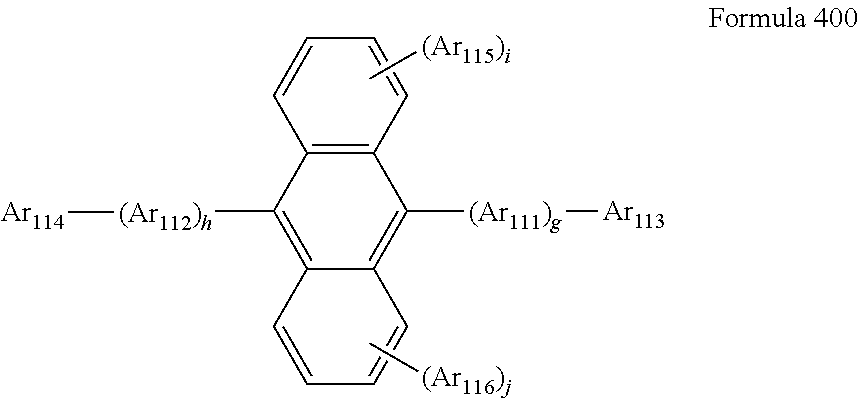

without being limited thereto.


1) Synthesis of Intermediate I-1

1) Synthesis of Intermediate I-10


1) Synthesis of Intermediate I-12

1) Synthesis of Intermediate I-17

1) Synthesis of Intermediate I-20
| TABLE 1 | ||
| MS/FAB | ||
| Compound | 1H NMR (CDCl3, 400 MHz) □ | found | calc. |
| 1 | δ = 8.07 (d, 1H), 7.99 (d, 1H), 7.95 (d, 1H), 7.84-7.79 | 594.20 | 594.21 |
| (m, 5H), 7.72-7.69 (m, 2H), 7.56-7.49 (m, 5H), | |||
| 7.46-7.43 (m, 2H), 7.40-7.35 (m, 3H), 7.34 (s, 2H), | |||
| 7.31-7.29 (m, 3H), 7.16-7.12 (m, 1H) | |||
| 5 | δ = 8.63 (dd, 1H), 8.50 (dd, 1H), 8.22 (d, 1H), 8.00 (d, | 595.21 | 595.20 |
| 1H), 7.98 (d, 1H), 7.85-7.79 (m, 6H), 7.72-.7.68 (m, | |||
| 2H), 7.62 (d, 1H), 7.54-7.45 (m, 3H), 7.41-7.38 (m, | |||
| 1H), 7.35-7.29 (m, 6H), 7.18-7.14 (m, 1H) | |||
| 15 | δ = 8.78-8.75 (m, 4H), 8.53 (d, 1H), 8.39 (d, 1H), 8.09 | 749.27 | 749.26 |
| (dd, 2H), 7.87-7.80 (m, 6H), 7.73-7.64 (m, 6H), | |||
| 7.54-7.51 (m, 2H), 7.45-7.38 (m, 3H), 7.35-7.29 (m, 5H), | |||
| 7.15-7.12 (m, 1H) | |||
| 21 | δ = 9.25 (d, 1H), 8.23 (dd, 2H), 8.09 (t, 2H), 7.94-7.82 | 671.22 | 671.24 |
| (m, 7H), 7.72-7.69 (m, 2H), 7.55-7.50 (m, 6H), | |||
| 7.43-7.28 (m, 8H), 7.16-7.12 (m, 1H) | |||
| 26 | δ = 8.08 (d, 1H), 8.04-8.02 (m, 2H), 7.99 (d, 1H), 7.95 | 670.25 | 670.24 |
| (d, 1H), 7.92 (d, 1H), 7.84-7.79 (m, 5H), 7.71-7.67 (m, | |||
| 3H), 7.58-7.43 (m, 7H), 7.40-7.29 (m, 8H), 7.18-7.13 | |||
| (m, 1H) | |||
| 28 | δ = 8.11 (d, 1H), 8.06 (d, 1H), 8.04-7.99 (m, 3H), 7.93 | 720.27 | 720.26 |
| (d, 1H), 7.91 (d, 1H), 7.86-7.77 (m, 5H), 7.73 (d, 1H), | |||
| 7.71-7.65 (m, 5H), 7.59-7.53 (m, 2H), 7.50-7.44 (m, | |||
| 3H), 7.41-7.31 (m, 7H), 7.12-7.08 (m, 2H) | |||
| 31 | δ = 8.60 (dd, 1H), 8.06 (d, 1H), 8.04-8.02 (m, 2H), 7.98 | 721.23 | 721.25 |
| (d, 1H), 7.96-7.85 (m, 4H), 7.83-7.77 (m, 5H), | |||
| 7.72-7.68 (m, 3H), 7.54 (d, 1H), 7.49-7.45 (m, 4H), | |||
| 7.41-7.29 (m, 7H), 7.16-7.12 (m, 2H) | |||
| 36 | δ = 8.96 (d, 1H), 8.60 (dd, 2H), 8.07 (d, 1H), 8.00 (d, | 671.25 | 671.24 |
| 1H), 7.95 (d, 1H), 7.84-7.70 (m, 7H), 7.55-7.48 (m, | |||
| 5H), 7.43-7.27 (m, 9H), 7.20-7.17 (m, 1H), 7.13-7.10 | |||
| (m, 1H) | |||
| 43 | δ = 8.93 (dd, 1H), 8.83-8.81 (m, 4H), 8.57 (d, 1H), 8.07 | 825.30 | 825.29 |
| (d, 1H), 8.00-7.94 (m, 3H), 7.83-7.76 (m, 4H), | |||
| 7.70-7.67 (m, 1H), 7.63-7.48 (m, 10H), 7.45-7.31 (m, 9H), | |||
| 7.19-7.16 (m, 1H) | |||
| 45 | δ = 8.07 (dd, 1H), 8.01-7.98 (m, 2H), 7.93 (d, 1H), | 644.25 | 644.23 |
| 7.86-7.80 (m, 7H), 7.74-7.65 (m, 4H), 7.60-7.45 (m, 6H), | |||
| 7.37-7.30 (m, 6H), 7.15-7.10 (m, 1H) | |||
| 55 | δ = 8.62 (dd, 1H), 8.49 (dd, 1H), 8.29 (dd, 1H), 8.22 (d, | 595.21 | 595.20 |
| 1H), 8.00-7.97 (m, 3H), 7.87 (dd, 1H), 7.83-7.78 (m, | |||
| 4H), 7.72-7.69 (m, 2H), 7.58-7.28 (m, 10H), 7.16-7.12 | |||
| (m, 1H) | |||
| 62 | δ = 8.07 (d, 1H), 8.03-8.01 (m, 2H), 7.97 (d, 1H), 7.93 | 670.25 | 670.24 |
| (d, 1H), 7.91 (d, 1H), 7.83-7.77 (m, 5H), 7.70-7.65 (m, | |||
| 3H), 7.58-7.44 (m, 7H), 7.39-7.31 (m, 8H), 7.17-7.13 | |||
| (m, 1H) | |||
| 65 | δ = 8.07 (d, 2H), 8.00-7.91 (m, 6H), 7.84-7.79 (m, 4H), | 884.30 | 884.29 |
| 7.70-7.66 (m, 2H), 7.56-7.48 (m, 10H), 7.43-7.31 (m, | |||
| 10H), 7.15-7.12 (m, 1H), 7.09-7.06 (m, 1H) | |||
| 75 | δ = 8.66-8.63 (m, 1H), 8.27-8.25 (m, 1H), 8.18-8.14 (m, | 644.25 | 644.23 |
| 2H), 8.03 (d, 1H), 7.98 (d, 1H), 7.82-7.76 (m, 2H), | |||
| 7.70-7.53 (m, 11H), 7.50-7.43 (m, 3H), 7.36 (d, 1H), | |||
| 7.29-7.20 (m, 2H), 7.15-7.10 (m, 3H) | |||
| 85 | δ = 8.08-8.06 (m, 1H), 8.01 (dd, 1H), 7.98 (d, 1H), 7.95 | 594.20 | 594.21 |
| (d, 1H), 7.85-7.76 (m, 3H), 7.73-7.40 (m, 14H), | |||
| 7.29-7.20 (m, 2H), 7.17-7.13 (m, 3H) | |||
| 91 | δ = 8.73 (d, 1H), 8.49 (dd, 1H), 8.30-8.25 (m, 1H), 8.17 | 545.20 | 545.19 |
| (d, 1H), 8.08 (d, 1H), 8.01 (d, 1H), 7.98-7.94 (m, 2H), | |||
| 7.81 (d, 1H), 7.76 (d, 1H), 7.63-7.58 (m, 4H), 7.53-7.50 | |||
| (m, 1H), 7.45-7.40 (m, 4H), 7.29-7.25 (m, 1H), | |||
| 7.12-7.05 (m, 3H) | |||


| TABLE 2 | ||||||||
| Half- | ||||||||
| Electron | Driving | Current | lifespan (hr | |||||
| transporting | voltage | density | Brightness | Efficiency | @100 mA/ | |||
| material | (V) | (mA/cm2) | (Cd/A) | (Cd/A) | Color | cm2) | ||
| Example 1 | Compound 1 | 4.60 | 50 | 3,980 | 8.12 | blue | 670 hr |
| Example 2 | Compound 5 | 4.82 | 50 | 3,650 | 7.85 | blue | 603 hr |
| Example 3 | Compound 15 | 5.15 | 50 | 3,275 | 6.68 | blue | 537 hr |
| Example 4 | Compound 21 | 4.67 | 50 | 3,520 | 7.36 | blue | 602 hr |
| Example 5 | Compound 26 | 4.93 | 50 | 3,865 | 7.97 | blue | 639 hr |
| Example 6 | Compound 43 | 4.85 | 50 | 3,705 | 7.41 | blue | 694 hr |
| Example 7 | Compound 45 | 5.06 | 50 | 3,810 | 8.05 | blue | 582 hr |
| Example 8 | Compound 55 | 5.25 | 50 | 3,600 | 7.17 | blue | 615 hr |
| Example 9 | Compound 62 | 5.18 | 50 | 3,385 | 7.53 | blue | 627 hr |
| Example 10 | Compound 65 | 5.39 | 50 | 3,210 | 7.02 | blue | 592 hr |
| Example 11 | Compound 75 | 5.50 | 50 | 3,080 | 6.53 | blue | 576 hr |
| Example 12 | Compound 91 | 5.06 | 50 | 3,380 | 7.34 | blue | 615 hr |
| Comparative | Compound 200 | 5.25 | 50 | 2,865 | 5.13 | blue | 337 hr |
| Example 1 | |||||||
| Comparative | Compound 201 | 4.73 | 50 | 3,325 | 6.25 | blue | 482 hr |
| Example 2 | |||||||
| Comparative | Compound 202 | 5.58 | 50 | 3,180 | 6.72 | blue | 318 hr |
| Example 3 | |||||||
Claims (20)


Applications Claiming Priority (2)
| Application Number | Priority Date | Filing Date | Title |
|---|---|---|---|
| KR10-2013-0118122 | 2013-10-02 | ||
| KR1020130118122A KR102191994B1 (en) | 2013-10-02 | 2013-10-02 | Compound and organic light emitting device comprising same |
Publications (2)
| Publication Number | Publication Date |
|---|---|
| US20150090965A1 US20150090965A1 (en) | 2015-04-02 |
| US9564596B2 true US9564596B2 (en) | 2017-02-07 |
Family
ID=52739187
Family Applications (1)
| Application Number | Title | Priority Date | Filing Date |
|---|---|---|---|
| US14/243,800 Active 2035-03-19 US9564596B2 (en) | 2013-10-02 | 2014-04-02 | Heterocyclic compound and organic light-emitting device comprising same |
Country Status (2)
| Country | Link |
|---|---|
| US (1) | US9564596B2 (en) |
| KR (1) | KR102191994B1 (en) |
Families Citing this family (14)
| Publication number | Priority date | Publication date | Assignee | Title |
|---|---|---|---|---|
| KR102050484B1 (en) | 2013-03-04 | 2019-12-02 | 삼성디스플레이 주식회사 | Anthracene derivatives and organic light emitting diodes comprising the derivatives |
| KR102107106B1 (en) | 2013-05-09 | 2020-05-07 | 삼성디스플레이 주식회사 | Styryl-based compound and organic light emitting diode comprising the same |
| KR102269131B1 (en) | 2013-07-01 | 2021-06-25 | 삼성디스플레이 주식회사 | Compound and organic light emitting device comprising same |
| US10062850B2 (en) | 2013-12-12 | 2018-08-28 | Samsung Display Co., Ltd. | Amine-based compounds and organic light-emitting devices comprising the same |
| US9638421B2 (en) * | 2014-02-14 | 2017-05-02 | Andritz Inc. | Startup burner assembly for recovery boiler and method |
| KR20150132795A (en) | 2014-05-16 | 2015-11-26 | 삼성디스플레이 주식회사 | Organic light emitting device |
| KR102327086B1 (en) * | 2014-06-11 | 2021-11-17 | 삼성디스플레이 주식회사 | Organic light-emitting devices |
| KR102343145B1 (en) | 2015-01-12 | 2021-12-27 | 삼성디스플레이 주식회사 | Condensed compound and organic light-emitting device comprising the same |
| KR102064993B1 (en) | 2017-05-31 | 2020-01-10 | 주식회사 엘지화학 | Novel hetero-cyclic compound and organic light emitting device comprising the same |
| WO2018221985A1 (en) * | 2017-05-31 | 2018-12-06 | 주식회사 엘지화학 | Novel heterocyclic compound and organic light emitting element using same |
| CN110294663B (en) * | 2018-03-23 | 2023-02-07 | 江苏三月科技股份有限公司 | Compound with anthracene as core and application thereof in organic electroluminescent device |
| US12453247B2 (en) * | 2019-03-27 | 2025-10-21 | Sharp Kabushiki Kaisha | Display device |
| US12096687B2 (en) * | 2020-07-22 | 2024-09-17 | Rohm And Haas Electronic Materials Korea Ltd. | Plurality of light-emitting materials, organic electroluminescent compound, and organic electroluminescent device comprising the same |
| CN113831292A (en) * | 2021-10-13 | 2021-12-24 | 上海传勤新材料有限公司 | Organic electron transport material containing benzimidazole and anthracene and application thereof |
Citations (14)
| Publication number | Priority date | Publication date | Assignee | Title |
|---|---|---|---|---|
| US5645948A (en) | 1996-08-20 | 1997-07-08 | Eastman Kodak Company | Blue organic electroluminescent devices |
| JPH1017860A (en) | 1996-06-28 | 1998-01-20 | Chisso Corp | Electroluminescent element characterized in using cyclopentadiene derivative |
| JPH1187067A (en) | 1997-09-05 | 1999-03-30 | Chisso Corp | Hole transport material having silacyclopentadiene ring |
| JP2004071500A (en) | 2002-08-09 | 2004-03-04 | Konica Minolta Holdings Inc | Organic electroluminescence element and display device |
| US20040053069A1 (en) | 2002-08-28 | 2004-03-18 | Fujitsu Limited | 1,3,6,8-Tetrasubstituted pyrene compound, organic EL element using the same, and organic EL display using the same |
| US20040137270A1 (en) | 2002-12-24 | 2004-07-15 | Lg Electronics Inc. | Organic electroluminescent device |
| US20050002857A1 (en) | 2003-05-06 | 2005-01-06 | Pez Guido Peter | Hydrogen storage by reversible hydrogenation of pi-conjugated substrates |
| KR100525408B1 (en) | 2002-12-24 | 2005-11-02 | 엘지전자 주식회사 | organic electroluminescence device |
| US20090019768A1 (en) | 2005-01-04 | 2009-01-22 | Air Products And Chemicals, Inc. | Dehydrogenation of Liquid Fuel in Microchannel Catalytic Reactor |
| JP2009029726A (en) | 2007-07-25 | 2009-02-12 | Toyo Ink Mfg Co Ltd | Compound having carbazolyl group and use thereof |
| JP2009123976A (en) | 2007-11-16 | 2009-06-04 | Toyo Ink Mfg Co Ltd | Organic electroluminescent element material and organic electroluminescent element. |
| KR20100094261A (en) | 2009-02-18 | 2010-08-26 | 덕산하이메탈(주) | Anthracene chemiclal and organic electroric element using the same, terminal thererof |
| US20150041773A1 (en) | 2013-08-09 | 2015-02-12 | Samsung Display Co., Ltd. | Anthracene-based compounds and organic light-emitting device including the same |
| US20150060787A1 (en) | 2013-08-28 | 2015-03-05 | Samsung Display Co., Ltd. | Compound and organic light-emitting device including the same |
Family Cites Families (4)
| Publication number | Priority date | Publication date | Assignee | Title |
|---|---|---|---|---|
| KR101894024B1 (en) * | 2011-04-22 | 2018-09-03 | 삼성디스플레이 주식회사 | Heterocyclic compound and Organic light emitting device comprising the same |
| KR20120125942A (en) * | 2011-05-09 | 2012-11-19 | 삼성디스플레이 주식회사 | Novel compound and organic light emitting device containing same |
| KR101873447B1 (en) * | 2011-06-22 | 2018-07-03 | 삼성디스플레이 주식회사 | Novel compound and organic light emitting device containing same |
| KR101891773B1 (en) * | 2011-10-18 | 2018-08-27 | 삼성디스플레이 주식회사 | Novel heterocyclic compound and organic light emitting device containing same |
-
2013
- 2013-10-02 KR KR1020130118122A patent/KR102191994B1/en active Active
-
2014
- 2014-04-02 US US14/243,800 patent/US9564596B2/en active Active
Patent Citations (17)
| Publication number | Priority date | Publication date | Assignee | Title |
|---|---|---|---|---|
| JPH1017860A (en) | 1996-06-28 | 1998-01-20 | Chisso Corp | Electroluminescent element characterized in using cyclopentadiene derivative |
| US5645948A (en) | 1996-08-20 | 1997-07-08 | Eastman Kodak Company | Blue organic electroluminescent devices |
| JPH1187067A (en) | 1997-09-05 | 1999-03-30 | Chisso Corp | Hole transport material having silacyclopentadiene ring |
| JP2004071500A (en) | 2002-08-09 | 2004-03-04 | Konica Minolta Holdings Inc | Organic electroluminescence element and display device |
| JP4060669B2 (en) | 2002-08-28 | 2008-03-12 | 富士フイルム株式会社 | 1,3,6,8-tetrasubstituted pyrene compound, organic EL device and organic EL display |
| US20040053069A1 (en) | 2002-08-28 | 2004-03-18 | Fujitsu Limited | 1,3,6,8-Tetrasubstituted pyrene compound, organic EL element using the same, and organic EL display using the same |
| US20040137270A1 (en) | 2002-12-24 | 2004-07-15 | Lg Electronics Inc. | Organic electroluminescent device |
| KR100525408B1 (en) | 2002-12-24 | 2005-11-02 | 엘지전자 주식회사 | organic electroluminescence device |
| US20050002857A1 (en) | 2003-05-06 | 2005-01-06 | Pez Guido Peter | Hydrogen storage by reversible hydrogenation of pi-conjugated substrates |
| US20090019768A1 (en) | 2005-01-04 | 2009-01-22 | Air Products And Chemicals, Inc. | Dehydrogenation of Liquid Fuel in Microchannel Catalytic Reactor |
| JP2009029726A (en) | 2007-07-25 | 2009-02-12 | Toyo Ink Mfg Co Ltd | Compound having carbazolyl group and use thereof |
| JP2009123976A (en) | 2007-11-16 | 2009-06-04 | Toyo Ink Mfg Co Ltd | Organic electroluminescent element material and organic electroluminescent element. |
| KR20100094261A (en) | 2009-02-18 | 2010-08-26 | 덕산하이메탈(주) | Anthracene chemiclal and organic electroric element using the same, terminal thererof |
| US20150041773A1 (en) | 2013-08-09 | 2015-02-12 | Samsung Display Co., Ltd. | Anthracene-based compounds and organic light-emitting device including the same |
| KR20150018229A (en) | 2013-08-09 | 2015-02-23 | 삼성디스플레이 주식회사 | Anthracene-based compounds and Organic light emitting device comprising the same |
| US20150060787A1 (en) | 2013-08-28 | 2015-03-05 | Samsung Display Co., Ltd. | Compound and organic light-emitting device including the same |
| KR20150025259A (en) | 2013-08-28 | 2015-03-10 | 삼성디스플레이 주식회사 | Compound and organic light emitting device comprising the same |
Non-Patent Citations (7)
| Title |
|---|
| 2009 Fall Assembly and Symposium. vol. 34, No. 2, Oct. 8, 2009, one page. |
| Adachi, C. et al., Confinement of charge carriers and molecular excitons within 5nm thick emitter layer in organic electroluminescent devices with a double heterostructure, Applied Physics Letters, vol. 57, (6), Aug. 6, 1990, 4 pgs. |
| Johansson, N. et al., Solid-State Amplified Spontaneous Emission in Some Spiro-Type Molecules: A New Concept for the Design of Solid-State Lasing Molecules, Advanced Materials, 1998, vol. 10, No. 14, pp. 1136-1141. |
| Sakamoto, Y. et al., Synthesis, Characterization, and Electron-Transport Property of Perfluorinated Phenylene Dendrimers, Journal American Chemical Society, vol. 122, No. 8, 2000, 2 pgs. |
| Tang, C. W. et al., Organic electroluminescent diodes, Applied Physics Letters, vol. 51, No. 12, Sep. 21, 1987, 4 pgs. |
| Tao, Y.T. et al., Sharp green electroluminescence from 1H-pyrazolo[3,4-b]quinoline-based light-emitting diodes, Applied Physics Letters, vol. 77, No. 11, Sep. 11, 2000, 4 pgs. |
| Yamaguchi, S. et al., Diphenylamino-Substituted 2,5-Diarylsiloles for Single-Layer Organic Electroluminescent Devices, Chemistry Letters 2001, 2 pgs. |
Also Published As
| Publication number | Publication date |
|---|---|
| KR102191994B1 (en) | 2020-12-17 |
| US20150090965A1 (en) | 2015-04-02 |
| KR20150039486A (en) | 2015-04-10 |
Similar Documents
| Publication | Publication Date | Title |
|---|---|---|
| US9564596B2 (en) | Heterocyclic compound and organic light-emitting device comprising same | |
| US9825234B2 (en) | Organic light-emitting diode | |
| US9705093B2 (en) | Heterocyclic compound and organic light-emitting device including the same | |
| US10256416B2 (en) | Compound and organic light-emitting device including the same | |
| US9368730B2 (en) | Heterocyclic compound and organic light-emitting device comprising the same | |
| US9559310B2 (en) | Compound with electron injection and/or electron transport capabilities and organic light-emitting device including the same | |
| US9419228B2 (en) | Heterocyclic compound and organic light-emitting diode comprising the same | |
| US9425407B2 (en) | Heterocyclic compound and organic light-emitting device including the same | |
| US9716234B2 (en) | Compound and organic light-emitting device including the same | |
| US20150243895A1 (en) | Compound and organic light-emitting device including the same | |
| US9252370B2 (en) | Heterocyclic compounds and organic light emitting devices including the same | |
| US9246109B2 (en) | Compound and organic light emitting device including the same | |
| US9455407B2 (en) | Compound and organic light-emitting device including the same | |
| US9276218B2 (en) | Arylamine compound and organic light-emitting device comprising same | |
| US9178162B2 (en) | Compound for organic light-emitting device and organic light-emitting device including the same | |
| US9806267B2 (en) | Compound and organic light-emitting device comprising the compound | |
| US9608211B2 (en) | Heterocyclic compound and organic light-emitting diode including the same | |
| US9437826B2 (en) | Heterocyclic compound and organic light-emitting device including the same | |
| US9196838B2 (en) | Organic compound and organic light-emitting device comprising the same | |
| US8546793B2 (en) | Organic light-emitting device | |
| US9553271B2 (en) | Compound and organic light-emitting device including the same | |
| US9437827B2 (en) | Heterocyclic compound and organic light-emitting device including the same | |
| US9406890B2 (en) | Compound and organic light-emitting diode including the same | |
| US9640768B2 (en) | Heterocyclic compound and orgainic light-emitting device including the same | |
| US9444056B2 (en) | Heterocyclic compound and organic light-emitting device including the same |
Legal Events
| Date | Code | Title | Description |
|---|---|---|---|
| AS | Assignment |
Owner name: SAMSUNG DISPLAY CO., LTD., KOREA, REPUBLIC OF Free format text: ASSIGNMENT OF ASSIGNORS INTEREST;ASSIGNORS:PARK, JUN-HA;JUN, MI-EUN;JEONG, EUN-JAE;REEL/FRAME:032610/0278 Effective date: 20140326 |
|
| FEPP | Fee payment procedure |
Free format text: PAYOR NUMBER ASSIGNED (ORIGINAL EVENT CODE: ASPN); ENTITY STATUS OF PATENT OWNER: LARGE ENTITY |
|
| STCF | Information on status: patent grant |
Free format text: PATENTED CASE |
|
| MAFP | Maintenance fee payment |
Free format text: PAYMENT OF MAINTENANCE FEE, 4TH YEAR, LARGE ENTITY (ORIGINAL EVENT CODE: M1551); ENTITY STATUS OF PATENT OWNER: LARGE ENTITY Year of fee payment: 4 |
|
| MAFP | Maintenance fee payment |
Free format text: PAYMENT OF MAINTENANCE FEE, 8TH YEAR, LARGE ENTITY (ORIGINAL EVENT CODE: M1552); ENTITY STATUS OF PATENT OWNER: LARGE ENTITY Year of fee payment: 8 |