US9564353B2 - FinFETs with reduced parasitic capacitance and methods of forming the same - Google Patents
FinFETs with reduced parasitic capacitance and methods of forming the same Download PDFInfo
- Publication number
- US9564353B2 US9564353B2 US13/763,242 US201313763242A US9564353B2 US 9564353 B2 US9564353 B2 US 9564353B2 US 201313763242 A US201313763242 A US 201313763242A US 9564353 B2 US9564353 B2 US 9564353B2
- Authority
- US
- United States
- Prior art keywords
- dielectric layer
- dielectric
- integrated circuit
- sidewall
- circuit structure
- Prior art date
- Legal status (The legal status is an assumption and is not a legal conclusion. Google has not performed a legal analysis and makes no representation as to the accuracy of the status listed.)
- Active
Links
- 238000000034 method Methods 0.000 title description 29
- 230000003071 parasitic effect Effects 0.000 title description 14
- 239000004065 semiconductor Substances 0.000 claims abstract description 81
- 239000000758 substrate Substances 0.000 claims abstract description 31
- 238000005530 etching Methods 0.000 claims abstract description 28
- 238000002955 isolation Methods 0.000 claims abstract description 7
- 239000003989 dielectric material Substances 0.000 claims description 11
- 230000015572 biosynthetic process Effects 0.000 description 11
- 239000000243 solution Substances 0.000 description 8
- 239000003990 capacitor Substances 0.000 description 7
- VYPSYNLAJGMNEJ-UHFFFAOYSA-N Silicium dioxide Chemical compound O=[Si]=O VYPSYNLAJGMNEJ-UHFFFAOYSA-N 0.000 description 5
- 238000013459 approach Methods 0.000 description 5
- 239000007789 gas Substances 0.000 description 5
- 239000000126 substance Substances 0.000 description 5
- QVGXLLKOCUKJST-UHFFFAOYSA-N atomic oxygen Chemical compound [O] QVGXLLKOCUKJST-UHFFFAOYSA-N 0.000 description 4
- 238000004140 cleaning Methods 0.000 description 4
- 238000004519 manufacturing process Methods 0.000 description 4
- 230000003647 oxidation Effects 0.000 description 4
- 238000007254 oxidation reaction Methods 0.000 description 4
- 239000001301 oxygen Substances 0.000 description 4
- 229910052760 oxygen Inorganic materials 0.000 description 4
- XUIMIQQOPSSXEZ-UHFFFAOYSA-N Silicon Chemical compound [Si] XUIMIQQOPSSXEZ-UHFFFAOYSA-N 0.000 description 3
- 238000005229 chemical vapour deposition Methods 0.000 description 3
- 238000000151 deposition Methods 0.000 description 3
- 230000005669 field effect Effects 0.000 description 3
- 239000000203 mixture Substances 0.000 description 3
- 229920002120 photoresistant polymer Polymers 0.000 description 3
- 229910052710 silicon Inorganic materials 0.000 description 3
- 239000010703 silicon Substances 0.000 description 3
- 229910052814 silicon oxide Inorganic materials 0.000 description 3
- IJGRMHOSHXDMSA-UHFFFAOYSA-N Atomic nitrogen Chemical compound N#N IJGRMHOSHXDMSA-UHFFFAOYSA-N 0.000 description 2
- 229910052581 Si3N4 Inorganic materials 0.000 description 2
- BOTDANWDWHJENH-UHFFFAOYSA-N Tetraethyl orthosilicate Chemical compound CCO[Si](OCC)(OCC)OCC BOTDANWDWHJENH-UHFFFAOYSA-N 0.000 description 2
- 238000000231 atomic layer deposition Methods 0.000 description 2
- 230000008021 deposition Effects 0.000 description 2
- 239000001257 hydrogen Substances 0.000 description 2
- 229910052739 hydrogen Inorganic materials 0.000 description 2
- 125000004435 hydrogen atom Chemical class [H]* 0.000 description 2
- 239000012212 insulator Substances 0.000 description 2
- 238000004518 low pressure chemical vapour deposition Methods 0.000 description 2
- 239000000463 material Substances 0.000 description 2
- 238000000623 plasma-assisted chemical vapour deposition Methods 0.000 description 2
- HQVNEWCFYHHQES-UHFFFAOYSA-N silicon nitride Chemical compound N12[Si]34N5[Si]62N3[Si]51N64 HQVNEWCFYHHQES-UHFFFAOYSA-N 0.000 description 2
- ZOXJGFHDIHLPTG-UHFFFAOYSA-N Boron Chemical compound [B] ZOXJGFHDIHLPTG-UHFFFAOYSA-N 0.000 description 1
- OKTJSMMVPCPJKN-UHFFFAOYSA-N Carbon Chemical compound [C] OKTJSMMVPCPJKN-UHFFFAOYSA-N 0.000 description 1
- GYHNNYVSQQEPJS-UHFFFAOYSA-N Gallium Chemical compound [Ga] GYHNNYVSQQEPJS-UHFFFAOYSA-N 0.000 description 1
- CBENFWSGALASAD-UHFFFAOYSA-N Ozone Chemical compound [O-][O+]=O CBENFWSGALASAD-UHFFFAOYSA-N 0.000 description 1
- NBIIXXVUZAFLBC-UHFFFAOYSA-N Phosphoric acid Chemical compound OP(O)(O)=O NBIIXXVUZAFLBC-UHFFFAOYSA-N 0.000 description 1
- OAICVXFJPJFONN-UHFFFAOYSA-N Phosphorus Chemical compound [P] OAICVXFJPJFONN-UHFFFAOYSA-N 0.000 description 1
- BLRPTPMANUNPDV-UHFFFAOYSA-N Silane Chemical compound [SiH4] BLRPTPMANUNPDV-UHFFFAOYSA-N 0.000 description 1
- 239000002253 acid Substances 0.000 description 1
- 230000002411 adverse Effects 0.000 description 1
- 230000004075 alteration Effects 0.000 description 1
- 229910052785 arsenic Inorganic materials 0.000 description 1
- RQNWIZPPADIBDY-UHFFFAOYSA-N arsenic atom Chemical compound [As] RQNWIZPPADIBDY-UHFFFAOYSA-N 0.000 description 1
- 229910052796 boron Inorganic materials 0.000 description 1
- 229910052799 carbon Inorganic materials 0.000 description 1
- 229910021419 crystalline silicon Inorganic materials 0.000 description 1
- 238000010790 dilution Methods 0.000 description 1
- 239000012895 dilution Substances 0.000 description 1
- 230000005684 electric field Effects 0.000 description 1
- 230000009969 flowable effect Effects 0.000 description 1
- 229910052733 gallium Inorganic materials 0.000 description 1
- 229910052732 germanium Inorganic materials 0.000 description 1
- GNPVGFCGXDBREM-UHFFFAOYSA-N germanium atom Chemical compound [Ge] GNPVGFCGXDBREM-UHFFFAOYSA-N 0.000 description 1
- 238000002513 implantation Methods 0.000 description 1
- 238000011065 in-situ storage Methods 0.000 description 1
- 229910052738 indium Inorganic materials 0.000 description 1
- APFVFJFRJDLVQX-UHFFFAOYSA-N indium atom Chemical compound [In] APFVFJFRJDLVQX-UHFFFAOYSA-N 0.000 description 1
- 229910052757 nitrogen Inorganic materials 0.000 description 1
- 230000001590 oxidative effect Effects 0.000 description 1
- 229910052698 phosphorus Inorganic materials 0.000 description 1
- 239000011574 phosphorus Substances 0.000 description 1
- 238000000206 photolithography Methods 0.000 description 1
- 238000005268 plasma chemical vapour deposition Methods 0.000 description 1
- 229910021332 silicide Inorganic materials 0.000 description 1
- 235000012239 silicon dioxide Nutrition 0.000 description 1
- 239000000377 silicon dioxide Substances 0.000 description 1
- 238000004088 simulation Methods 0.000 description 1
- 238000006467 substitution reaction Methods 0.000 description 1
- 239000004094 surface-active agent Substances 0.000 description 1
- 239000010409 thin film Substances 0.000 description 1
- 238000007740 vapor deposition Methods 0.000 description 1
Images


Classifications
-
- H—ELECTRICITY
- H01—ELECTRIC ELEMENTS
- H01L—SEMICONDUCTOR DEVICES NOT COVERED BY CLASS H10
- H01L21/00—Processes or apparatus adapted for the manufacture or treatment of semiconductor or solid state devices or of parts thereof
- H01L21/70—Manufacture or treatment of devices consisting of a plurality of solid state components formed in or on a common substrate or of parts thereof; Manufacture of integrated circuit devices or of parts thereof
- H01L21/71—Manufacture of specific parts of devices defined in group H01L21/70
- H01L21/76—Making of isolation regions between components
- H01L21/762—Dielectric regions, e.g. EPIC dielectric isolation, LOCOS; Trench refilling techniques, SOI technology, use of channel stoppers
- H01L21/76224—Dielectric regions, e.g. EPIC dielectric isolation, LOCOS; Trench refilling techniques, SOI technology, use of channel stoppers using trench refilling with dielectric materials
- H01L21/76232—Dielectric regions, e.g. EPIC dielectric isolation, LOCOS; Trench refilling techniques, SOI technology, use of channel stoppers using trench refilling with dielectric materials of trenches having a shape other than rectangular or V-shape, e.g. rounded corners, oblique or rounded trench walls
-
- H—ELECTRICITY
- H01—ELECTRIC ELEMENTS
- H01L—SEMICONDUCTOR DEVICES NOT COVERED BY CLASS H10
- H01L21/00—Processes or apparatus adapted for the manufacture or treatment of semiconductor or solid state devices or of parts thereof
- H01L21/70—Manufacture or treatment of devices consisting of a plurality of solid state components formed in or on a common substrate or of parts thereof; Manufacture of integrated circuit devices or of parts thereof
- H01L21/71—Manufacture of specific parts of devices defined in group H01L21/70
- H01L21/76—Making of isolation regions between components
- H01L21/762—Dielectric regions, e.g. EPIC dielectric isolation, LOCOS; Trench refilling techniques, SOI technology, use of channel stoppers
- H01L21/76224—Dielectric regions, e.g. EPIC dielectric isolation, LOCOS; Trench refilling techniques, SOI technology, use of channel stoppers using trench refilling with dielectric materials
-
- H—ELECTRICITY
- H01—ELECTRIC ELEMENTS
- H01L—SEMICONDUCTOR DEVICES NOT COVERED BY CLASS H10
- H01L29/00—Semiconductor devices specially adapted for rectifying, amplifying, oscillating or switching and having potential barriers; Capacitors or resistors having potential barriers, e.g. a PN-junction depletion layer or carrier concentration layer; Details of semiconductor bodies or of electrodes thereof ; Multistep manufacturing processes therefor
- H01L29/02—Semiconductor bodies ; Multistep manufacturing processes therefor
- H01L29/06—Semiconductor bodies ; Multistep manufacturing processes therefor characterised by their shape; characterised by the shapes, relative sizes, or dispositions of the semiconductor regions ; characterised by the concentration or distribution of impurities within semiconductor regions
- H01L29/0603—Semiconductor bodies ; Multistep manufacturing processes therefor characterised by their shape; characterised by the shapes, relative sizes, or dispositions of the semiconductor regions ; characterised by the concentration or distribution of impurities within semiconductor regions characterised by particular constructional design considerations, e.g. for preventing surface leakage, for controlling electric field concentration or for internal isolations regions
- H01L29/0642—Isolation within the component, i.e. internal isolation
- H01L29/0649—Dielectric regions, e.g. SiO2 regions, air gaps
-
- H—ELECTRICITY
- H01—ELECTRIC ELEMENTS
- H01L—SEMICONDUCTOR DEVICES NOT COVERED BY CLASS H10
- H01L29/00—Semiconductor devices specially adapted for rectifying, amplifying, oscillating or switching and having potential barriers; Capacitors or resistors having potential barriers, e.g. a PN-junction depletion layer or carrier concentration layer; Details of semiconductor bodies or of electrodes thereof ; Multistep manufacturing processes therefor
- H01L29/66—Types of semiconductor device ; Multistep manufacturing processes therefor
- H01L29/66007—Multistep manufacturing processes
- H01L29/66075—Multistep manufacturing processes of devices having semiconductor bodies comprising group 14 or group 13/15 materials
- H01L29/66227—Multistep manufacturing processes of devices having semiconductor bodies comprising group 14 or group 13/15 materials the devices being controllable only by the electric current supplied or the electric potential applied, to an electrode which does not carry the current to be rectified, amplified or switched, e.g. three-terminal devices
- H01L29/66409—Unipolar field-effect transistors
- H01L29/66477—Unipolar field-effect transistors with an insulated gate, i.e. MISFET
- H01L29/66787—Unipolar field-effect transistors with an insulated gate, i.e. MISFET with a gate at the side of the channel
- H01L29/66795—Unipolar field-effect transistors with an insulated gate, i.e. MISFET with a gate at the side of the channel with a horizontal current flow in a vertical sidewall of a semiconductor body, e.g. FinFET, MuGFET
-
- H—ELECTRICITY
- H01—ELECTRIC ELEMENTS
- H01L—SEMICONDUCTOR DEVICES NOT COVERED BY CLASS H10
- H01L29/00—Semiconductor devices specially adapted for rectifying, amplifying, oscillating or switching and having potential barriers; Capacitors or resistors having potential barriers, e.g. a PN-junction depletion layer or carrier concentration layer; Details of semiconductor bodies or of electrodes thereof ; Multistep manufacturing processes therefor
- H01L29/66—Types of semiconductor device ; Multistep manufacturing processes therefor
- H01L29/68—Types of semiconductor device ; Multistep manufacturing processes therefor controllable by only the electric current supplied, or only the electric potential applied, to an electrode which does not carry the current to be rectified, amplified or switched
- H01L29/76—Unipolar devices, e.g. field effect transistors
- H01L29/772—Field effect transistors
- H01L29/78—Field effect transistors with field effect produced by an insulated gate
- H01L29/785—Field effect transistors with field effect produced by an insulated gate having a channel with a horizontal current flow in a vertical sidewall of a semiconductor body, e.g. FinFET, MuGFET
Definitions
- Fin Field-Effect Transistors were thus developed.
- the FinFETs include vertical semiconductor fins above a substrate.
- the semiconductor fins are used to form source and drain regions, and channel regions between the source and drain regions. Shallow Trench Isolation (STI) regions are formed to define the semiconductor fins.
- the FinFETs also include gate stacks, which are formed on the sidewalls and the top surfaces of the semiconductor fins.
- various wet etch steps and clean steps are performed. These steps cause the recess of the top surfaces of STI regions. As a result of the wet etch steps and clean steps, the center portions of the top surfaces of the STI regions are lower than edge portions of the top surfaces of the STI regions.
- the STI regions with such a surface profile are known as having a (concave shape) smiling profile.
- parasitic capacitors are formed between the gate electrodes of the FinFETs and the neighboring semiconductor strip, wherein the STI regions act as the insulators of the parasitic capacitors.
- the parasitic capacitance of the parasitic capacitors adversely affects the performance of the respective integrated circuit, and needs to be reduced.
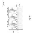
- FIGS. 1 through 10C are cross-sectional views of intermediate stages in the manufacturing of Shallow Trench Isolation (STI) regions and Fin Field-Effect Transistors (FinFETs) in accordance with some exemplary embodiments; and
- FIG. 11 illustrates parasitic capacitance ratios as a function of height differences of STI regions.
- Shallow Trench Isolation (STI) regions, Fin Field-Effect Transistors (FinFETs), and methods of forming the same are provided.
- the intermediate stages in the formation of the STI regions and the FinFETs are illustrated in accordance with exemplary embodiments. The variations of the embodiment are discussed.
- like reference numbers are used to designate like elements.
- semiconductor substrate 20 which is a part of semiconductor wafer 100 , is provided.
- semiconductor substrate 20 includes crystalline silicon.
- Other commonly used materials such as carbon, germanium, gallium, boron, arsenic, nitrogen, indium, and/or phosphorus, and the like, may also be included in semiconductor substrate 20 .
- Semiconductor substrate 20 may be a bulk substrate or a Semiconductor-On-Insulator (SOI) substrate.
- SOI Semiconductor-On-Insulator
- Pad layer 22 and mask layer 24 are formed on semiconductor substrate 20 .
- Pad layer 22 may be a thin film comprising silicon oxide formed, for example, using a thermal oxidation process.
- Pad layer 22 may act as an adhesion layer between semiconductor substrate 20 and mask layer 24 .
- Pad layer 22 may also act as an etch stop layer for etching mask layer 24 .
- mask layer 24 is formed of silicon nitride, for example, using Low-Pressure Chemical Vapor Deposition (LPCVD).
- LPCVD Low-Pressure Chemical Vapor Deposition
- mask layer 24 is formed by thermal nitridation of silicon, Plasma Enhanced Chemical Vapor Deposition (PECVD), or plasma anodic nitridation.
- PECVD Plasma Enhanced Chemical Vapor Deposition
- Mask layer 24 is used as a hard mask during subsequent photolithography processes.
- Photo resist 26 is formed on mask layer 24 and is then patterned, forming openings 28 in photo resist 26 .
- mask layer 24 and pad layer 22 are etched through openings 28 , exposing underlying semiconductor substrate 20 .
- the exposed semiconductor substrate 20 is then etched, forming trenches 32 .
- the portions of semiconductor substrate 20 between neighboring trenches 32 form semiconductor strips 30 .
- Trenches 32 may be strips (when viewed in the top view of wafer 100 ) that are parallel to each other, and closely located from each other.
- photo resist 26 FIG. 1
- a cleaning step may be performed to remove a native oxide of semiconductor substrate 20 .
- the cleaning may be performed using diluted hydrofluoric (HF) acid, for example.
- liner oxide 34 is formed in trenches 32 and on the sidewalls of semiconductor strips 30 , as is shown in FIG. 3 .
- Liner oxide 34 may be a conformal layer whose horizontal portions and vertical portions have thicknesses close to each other.
- Liner oxide 34 may be a thermal oxide having a thickness between about 10 ⁇ to about 100 ⁇ .
- liner oxide 34 is formed by oxidizing wafer 100 in an oxygen-containing environment, for example, through Local Oxidation of Silicon (LOCOS), wherein oxygen (O 2 ) may be included in the respective process gas.
- LOCOS Local Oxidation of Silicon
- liner oxide 34 is formed using In-Situ Steam Generation (ISSG), for example, with moisture or a combined gas of hydrogen (H 2 ) and oxygen (O 2 ) used to oxidize semiconductor strips 30 .
- the ISSG oxidation may be performed at an elevated temperature.
- liner oxide 34 may be formed using a deposition technique such as Sub Atmospheric Vapor Deposition (SACVD).
- SACVD Sub Atmospheric Vapor Deposition
- the formation of liner oxide 34 may result in the rounding of the corners of trenches 32 , which reduces the electrical fields of the resulting FinFET, and hence improves the performance of the resulting integrated circuit.
- Liner oxide 34 may comprise silicon dioxide or other dielectric materials.
- the density of liner oxide 34 may be between about 2.2 grams/cm 3 and about 2.3 grams/cm 3 in some embodiments. In alternative embodiments, the formation of liner oxide 34 is skipped.
- FIG. 4 illustrates the formation of dielectric layer 36 .
- Dielectric layer 36 partially fills trenches 32 , and some portions of trenches 32 remain unfilled.
- Dielectric layer 36 may be conformal or close to conformal, wherein thickness T1 of the vertical portions of dielectric layer 36 is close to thickness T2 of the horizontal portions of dielectric layer 36 .
- thickness T2 is greater than thickness T1.
- thickness T1 which may be measured at the level of the top surfaces of semiconductor strips 30 , may be greater than about 5 nm, so that in subsequent process steps, STI regions 40 ( FIGS. 10A, 10B, and 10C ) may have a desirable top surface profile.
- dielectric layer 36 may be selected from Chemical Vapor Deposition (CVD), Atomic Layer Deposition (ALD), Flowable Chemical Vapor Deposition (FCVD), and the like.
- CVD Chemical Vapor Deposition
- ALD Atomic Layer Deposition
- FCVD Flowable Chemical Vapor Deposition
- liner oxide 34 is in contact with semiconductor strip 30
- dielectric layer 36 is formed on, and contacting, liner oxide 34 .
- liner oxide 34 is not formed, and hence dielectric layer 36 is in contact with the sidewalls of semiconductor strips 30 .
- FIG. 6B illustrates a structure with dielectric layer 36 contacting semiconductor strips 30 .
- the material of dielectric layer 36 includes, and is not limited to, a low-k dielectric material having a k value lower than about 3.0, a porous dielectric material, and the like.
- dielectric layer 36 comprises silicon, oxygen, hydrogen, and combinations thereof.
- the density of dielectric layer 36 may be lower than about 2.0 grams/cm 3 , and may be lower than the density of liner oxide 34 , for example, with a density difference greater than about 0.2 grams/cm 3 .
- dielectric region 38 The top surface of dielectric region 38 is higher than the top surface of mask layer 24 .
- Dielectric region 38 may include silicon oxide, and hence is referred to as oxide 38 hereinafter, although other dielectric materials, such as SiN, SiC, or the like, may also be used.
- oxide 38 is formed using High Aspect-Ratio Process (HARP), High-Density Plasma CVD (HDPCVD), or the like.
- HTP High Aspect-Ratio Process
- HDPCVD High-Density Plasma CVD
- the respective process gases may include tetraethylorthosilicate (TEOS) and O 3 (ozone) (in the HARP process), or SiH 4 and O 2 (in the HDPCVD process).
- TEOS tetraethylorthosilicate
- O 3 ozone
- SiH 4 and O 2 in the HDPCVD process
- FIG. 6A A planarization such as Chemical Mechanical Polish (CMP) is then performed, as shown in FIG. 6A , and hence STI regions 40 are formed, which include the remaining portions of liner oxide 34 , dielectric layer 36 , and dielectric region 38 .
- dielectric layer 36 and dielectric region 38 may be separated into a plurality of discrete portions, which are referred to as dielectric layers 36 and dielectric regions 38 , respectively.
- Mask layer 24 is used as the CMP stop layer, and hence the top surface of mask layer 24 is substantially level with the top surface of dielectric regions 38 and the top surfaces of dielectric layers 36 .
- the discrete portions of liner oxide 34 are referred to as liner oxide layers 34 hereinafter.
- FIG. 6B illustrates wafer 100 in accordance with alternative embodiments, in which the formation of liner oxide 34 is skipped, and dielectric layers 36 are in contact with the sidewalls of semiconductor strips 30 .
- FIG. 7 illustrates the removal of mask layer 24 .
- Mask layer 24 if formed of silicon nitride, may be removed in a wet process using hot H 3 PO 4 .
- the structure shown in FIG. 7 is used to form semiconductor fins through the recessing of STI regions 40 , and pad layer 22 is also removed, wherein the resulting structure is shown in FIG. 8 .
- the portions of semiconductor strips 30 protruding over the top surfaces of the remaining STI regions 40 become semiconductor fins 42 .
- the recessing of STI regions 40 may be performed using a dry etch process or a wet etch process.
- the recessing of STI regions 40 is performed using a dry etch method, in which the process gases including NH 3 and HF are used. In alternative embodiments, the recessing of STI regions 40 is performed using a wet etch method, in which the etchant solution includes NF 3 and HF. In yet other embodiments, the recessing of STI regions 40 is performed using a dilution HF solution, which may have an HF concentration lower than about 1 percent.
- dielectric layers 36 have an etching rate E 2 higher than the etching rate E 1 of liner oxide layers 34 and the etching rate E 3 of dielectric regions 38 .
- etching rate ratio E 2 /E 3 may be greater than about 1.2.
- etching rate ratio E 2 /E 1 may also be greater than about 1.2 when etched by diluted HF.
- the etching rate ratios E 2 /E 1 and E 2 /E 3 may be different from the etching rate ratios obtained by using diluted HF solution as the reference etchant.
- etching rate ratios E 2 /E 1 and E 2 /E 3 may still be greater than 1.0.
- the top surfaces of dielectric layers 36 may be lower than the top surfaces of dielectric regions 38 .
- the respective top surfaces of dielectric layers 36 are schematically illustrated using dashed lines 44 .
- various approaches may be used to further recess the top surfaces of dielectric layer 36 more than the top surfaces of dielectric regions 38 and liner oxides 34 .
- fine tuning the pressure, the temperature, and/or the NH 3 /HF gas ratio may result in more dielectric layer 36 to be etched than dielectric regions 38 and liner oxides 34 , and hence result in a convex STI surface.
- STI regions 40 are recessed to form semiconductor fins 42 , a plurality of process steps are formed on semiconductor fins 42 , which process steps may include well implantations, dummy gate (not shown) formation and removal, a plurality of cleaning steps, and the like. Accordingly, the profile of the top surfaces of STI regions 40 is further shaped.
- chemicals are used. For example, in the cleaning steps, diluted HF or surfactant contented diluted HF may be used. These chemicals attack STI regions 40 .
- dielectric layers 36 when attacked by these chemicals, are etched faster than liner oxide layers 34 and/or dielectric regions 38 .
- the structures shown in FIGS. 9A, 9B, and 9C thus may be formed.
- FIG. 9A illustrates one of the likely top surface profiles of STI regions 40 . Since etching rate ratios E 2 /E 1 and E 2 /E 3 are greater than 1.0, and/or the density of dielectric layers 36 is lower than that of liner oxide layers 34 and/or dielectric regions 38 , dielectric layers 36 are recessed more than liner oxide layers 34 and/or dielectric regions 38 by the chemicals. The highest point of dielectric region 38 , which is between two neighboring semiconductor strips 30 , is higher than the lowest point of the respective dielectric layer 36 (in the same STI region 40 ) by height different ⁇ H1, which may be greater than about 2 nm. The resulting STI regions 40 are hence referred to as having convex-shape top surfaces.
- liner oxide layers 34 are much thinner than dielectric layers 36 , and hence liner oxide layers 34 are also recessed much more than dielectric regions 38 , partially due to the etching of liner oxide layers 34 from their side surfaces, which side surfaces are exposed when dielectric layers 36 are recessed.
- the resulting profile of the top surfaces of STI regions 40 is shown in FIG. 9A , in which the top surfaces of the sidewall portions of liner oxide layers 34 and dielectric layers 36 are substantially leveled with each other, and are lower than the top surface of the respective dielectric regions 38 .
- the top surfaces of liner oxides 34 and dielectric regions 38 are both higher than that of the respective dielectric layers 36 in the same STI region 40 .
- the top surfaces of a dielectric layer 36 may have a lowest point close to the middle point that has equal distances from the respective neighboring dielectric region 38 and liner oxide layer 34 .
- the top surface of dielectric layer 36 becomes increasingly higher in positions closer to the respective neighboring dielectric region 38 or liner oxide 34 .
- each of dielectric regions 38 is over a bottom portion of a respective dielectric layer 36 , and a sidewall of the dielectric region 38 is in contact with a sidewall portion of dielectric layer 36 .
- FIG. 9C illustrates wafer 100 in accordance with yet alternative embodiments, wherein no liner oxide is formed. Accordingly, the sidewall portions of dielectric layers 36 are in physical contact with the sidewalls of semiconductor strips 30 . Again, the top surfaces of dielectric layers 36 are higher than the top surfaces of dielectric regions 38 . In each of FIGS. 9A, 9B, and 9C , the middle portions of the top surface of dielectric regions 38 may be higher than the edge portions of the top surface of the respective dielectric regions 38 .
- FIGS. 10A, 10B, and 10C illustrate FinFETs 52 formed from the structures shown in FIGS. 9A, 9B, and 9C , respectively.
- gate dielectric 48 is formed to cover the top surfaces and sidewalls of fins 42 .
- Gate dielectric 48 may be formed through a thermal oxidation, and hence may include thermal silicon oxide.
- gate dielectric 48 may be formed through a deposition step, and may comprise high-k dielectric materials.
- Gate electrode 50 is then formed on gate dielectric 48 . In some embodiments, gate electrode 50 covers more than one fin 42 , so that the resulting FinFET 66 comprises more than one fin 42 .
- each of fins 42 may be used to form one FinFET.
- the remaining components of the FinFET 52 including source and drain regions and source and drain silicides (not shown), are then formed. The formation processes of these components are known in the art, and hence are not repeated herein.
- Gate dielectric 48 and gate electrode 50 may be formed using a gate-first approach or a gate last approach. The details of the gate-first approach or a gate last approach are not described herein.
- STI regions 40 have convex shapes, and hence the parasitic capacitance, which are shown as parasitic capacitors 54 in FIGS. 10A, 10B, and 10C , are reduced compared to that in FinFETs whose STI regions have concave (smiling) profiles.
- Parasitic capacitors 54 are formed between gate electrode 50 and the bottom portions of semiconductor strips 30 , which bottom portions are below semiconductor fins 42 .
- FIG. 11 illustrates simulation results, wherein parasitic capacitance ratios are illustrated as a function of height difference ⁇ H1 ( FIGS. 9A, 9B, and 9C ).
- the parasitic capacitance ratio is obtained by normalizing the capacitance of parasitic capacitors 54 ( FIGS. 10A, 10B, and 10C ) of a FinFET whose ⁇ H1 is greater than zero nm by the capacitance of parasitic capacitors 54 ( FIGS. 10A, 10B, and 10C ) of a FinFET whose ⁇ H1 is equal to zero nm.
- the results in FIG. 11 indicate that with the increase in height difference ⁇ H1, the parasitic capacitances are reduced.
- an integrated circuit structure includes a semiconductor substrate, a semiconductor strip over a portion of the semiconductor substrate, and an STI region on a side of the semiconductor strip.
- the STI region includes a dielectric layer, which includes a sidewall portion on a sidewall of the semiconductor strip and a bottom portion.
- the dielectric layer has a first etching rate when etched using a diluted HF solution.
- the STI region further includes a dielectric region over the bottom portion of the dielectric layer.
- the dielectric region has an edge contacting an edge of the sidewall portion of the dielectric layer.
- the dielectric region has a second etching rate when etched using the diluted HF solution, wherein the second etching rate is smaller than the first etching rate.
- an integrated circuit structure includes a semiconductor substrate, an opening extending into the semiconductor substrate, and a semiconductor strip on a side of the opening.
- the semiconductor strip is a portion of the semiconductor substrate.
- a liner oxide is on a bottom and sidewalls of the opening.
- the liner oxide includes a first sidewall portion contacting a sidewall of the semiconductor strip, and a first bottom portion.
- a dielectric layer is over the liner oxide and includes a second sidewall portion, and a second bottom portion overlapping the first bottom portion.
- a dielectric region is over the second bottom portion, with the second sidewall portion between the first sidewall portion and the dielectric region.
- a top surface of the second sidewall portion is lower than a top surface of the dielectric region.
- a method includes forming an opening extending from a top surface of a semiconductor substrate into the semiconductor substrate, wherein a portion of the semiconductor substrate forms a semiconductor strip exposing to the opening.
- a dielectric layer is formed in the opening, wherein the dielectric layer has a first etching rate when etched using a diluted HF solution.
- a dielectric region is formed over the dielectric layer and filling the remaining portion of the opening.
- the dielectric region has a second etching rate when etched using the diluted HF solution wherein the first etching rate is greater than the second etching rate.
- the method further includes performing a planarization to remove excess portions of the dielectric layer and the dielectric region, wherein the excess portions are over the top surface of a semiconductor substrate. The remaining portions of the dielectric layer and the dielectric region form an STI region.
Landscapes
- Engineering & Computer Science (AREA)
- Microelectronics & Electronic Packaging (AREA)
- Power Engineering (AREA)
- Physics & Mathematics (AREA)
- Condensed Matter Physics & Semiconductors (AREA)
- General Physics & Mathematics (AREA)
- Computer Hardware Design (AREA)
- Manufacturing & Machinery (AREA)
- Ceramic Engineering (AREA)
- Element Separation (AREA)
- Insulated Gate Type Field-Effect Transistor (AREA)
- Thin Film Transistor (AREA)
Abstract
An integrated circuit structure includes a semiconductor substrate, a semiconductor strip over a portion of the semiconductor substrate, and a Shallow Trench Isolation (STI) region on a side of the semiconductor strip. The STI region includes a dielectric layer, which includes a sidewall portion on a sidewall of the semiconductor strip and a bottom portion. The dielectric layer has a first etching rate when etched using a diluted HF solution. The STI region further includes a dielectric region over the bottom portion of the dielectric layer. The dielectric region has an edge contacting an edge of the sidewall portion of the dielectric layer. The dielectric region has a second etching rate when etched using the diluted HF solution, wherein the second etching rate is smaller than the first etching rate.
Description
With the increasing down-scaling of integrated circuits and the increasingly demanding requirements to the speed of integrated circuits, transistors need to have higher drive currents with increasingly smaller dimensions. Fin Field-Effect Transistors (FinFET) were thus developed. The FinFETs include vertical semiconductor fins above a substrate. The semiconductor fins are used to form source and drain regions, and channel regions between the source and drain regions. Shallow Trench Isolation (STI) regions are formed to define the semiconductor fins. The FinFETs also include gate stacks, which are formed on the sidewalls and the top surfaces of the semiconductor fins.
In the formation of the STI regions and the formation of the FinFETs, various wet etch steps and clean steps are performed. These steps cause the recess of the top surfaces of STI regions. As a result of the wet etch steps and clean steps, the center portions of the top surfaces of the STI regions are lower than edge portions of the top surfaces of the STI regions. The STI regions with such a surface profile are known as having a (concave shape) smiling profile.
In some FinFET, there are semiconductor strips underlying the semiconductor fins. In the respective FinFETs, parasitic capacitors are formed between the gate electrodes of the FinFETs and the neighboring semiconductor strip, wherein the STI regions act as the insulators of the parasitic capacitors. The parasitic capacitance of the parasitic capacitors adversely affects the performance of the respective integrated circuit, and needs to be reduced.
For a more complete understanding of the embodiments, and the advantages thereof, reference is now made to the following descriptions taken in conjunction with the accompanying drawings, in which:
The making and using of the embodiments of the disclosure are discussed in detail below. It should be appreciated, however, that the embodiments provide many applicable concepts that can be embodied in a wide variety of specific contexts. The specific embodiments discussed are illustrative, and do not limit the scope of the disclosure.
Shallow Trench Isolation (STI) regions, Fin Field-Effect Transistors (FinFETs), and methods of forming the same are provided. The intermediate stages in the formation of the STI regions and the FinFETs are illustrated in accordance with exemplary embodiments. The variations of the embodiment are discussed. Throughout the various views and illustrative embodiments, like reference numbers are used to designate like elements.
Referring to FIG. 1 , semiconductor substrate 20, which is a part of semiconductor wafer 100, is provided. In some embodiments, semiconductor substrate 20 includes crystalline silicon. Other commonly used materials, such as carbon, germanium, gallium, boron, arsenic, nitrogen, indium, and/or phosphorus, and the like, may also be included in semiconductor substrate 20. Semiconductor substrate 20 may be a bulk substrate or a Semiconductor-On-Insulator (SOI) substrate.
Referring to FIG. 2 , mask layer 24 and pad layer 22 are etched through openings 28, exposing underlying semiconductor substrate 20. The exposed semiconductor substrate 20 is then etched, forming trenches 32. The portions of semiconductor substrate 20 between neighboring trenches 32 form semiconductor strips 30. Trenches 32 may be strips (when viewed in the top view of wafer 100) that are parallel to each other, and closely located from each other. After the etching of semiconductor substrate 20, photo resist 26 (FIG. 1 ) is removed. Next, a cleaning step may be performed to remove a native oxide of semiconductor substrate 20. The cleaning may be performed using diluted hydrofluoric (HF) acid, for example.
In accordance with some embodiments, liner oxide 34 is formed in trenches 32 and on the sidewalls of semiconductor strips 30, as is shown in FIG. 3 . Liner oxide 34 may be a conformal layer whose horizontal portions and vertical portions have thicknesses close to each other. Liner oxide 34 may be a thermal oxide having a thickness between about 10 Å to about 100 Å. In some embodiments, liner oxide 34 is formed by oxidizing wafer 100 in an oxygen-containing environment, for example, through Local Oxidation of Silicon (LOCOS), wherein oxygen (O2) may be included in the respective process gas. In other embodiments, liner oxide 34 is formed using In-Situ Steam Generation (ISSG), for example, with moisture or a combined gas of hydrogen (H2) and oxygen (O2) used to oxidize semiconductor strips 30. The ISSG oxidation may be performed at an elevated temperature. In yet other embodiments, liner oxide 34 may be formed using a deposition technique such as Sub Atmospheric Vapor Deposition (SACVD). The formation of liner oxide 34 may result in the rounding of the corners of trenches 32, which reduces the electrical fields of the resulting FinFET, and hence improves the performance of the resulting integrated circuit. Liner oxide 34 may comprise silicon dioxide or other dielectric materials. The density of liner oxide 34 may be between about 2.2 grams/cm3 and about 2.3 grams/cm3 in some embodiments. In alternative embodiments, the formation of liner oxide 34 is skipped.
The material of dielectric layer 36 includes, and is not limited to, a low-k dielectric material having a k value lower than about 3.0, a porous dielectric material, and the like. In some embodiments, dielectric layer 36 comprises silicon, oxygen, hydrogen, and combinations thereof. The density of dielectric layer 36 may be lower than about 2.0 grams/cm3, and may be lower than the density of liner oxide 34, for example, with a density difference greater than about 0.2 grams/cm3.
Next, referring to FIG. 5 , the remaining portions of trenches 32 are filled with a dielectric material to form dielectric region 38. The top surface of dielectric region 38 is higher than the top surface of mask layer 24. Dielectric region 38 may include silicon oxide, and hence is referred to as oxide 38 hereinafter, although other dielectric materials, such as SiN, SiC, or the like, may also be used. In some embodiments, oxide 38 is formed using High Aspect-Ratio Process (HARP), High-Density Plasma CVD (HDPCVD), or the like. In the deposition of dielectric region 38, the respective process gases may include tetraethylorthosilicate (TEOS) and O3 (ozone) (in the HARP process), or SiH4 and O2 (in the HDPCVD process).
A planarization such as Chemical Mechanical Polish (CMP) is then performed, as shown in FIG. 6A , and hence STI regions 40 are formed, which include the remaining portions of liner oxide 34, dielectric layer 36, and dielectric region 38. After the CMP, dielectric layer 36 and dielectric region 38 may be separated into a plurality of discrete portions, which are referred to as dielectric layers 36 and dielectric regions 38, respectively. Mask layer 24 is used as the CMP stop layer, and hence the top surface of mask layer 24 is substantially level with the top surface of dielectric regions 38 and the top surfaces of dielectric layers 36. Furthermore, the discrete portions of liner oxide 34 are referred to as liner oxide layers 34 hereinafter. FIG. 6B illustrates wafer 100 in accordance with alternative embodiments, in which the formation of liner oxide 34 is skipped, and dielectric layers 36 are in contact with the sidewalls of semiconductor strips 30.
In the recessing of STI regions 40, liner oxide layers 34, dielectric layers 36, and dielectric regions 38 are all etched. In some embodiments, dielectric layers 36 have an etching rate E2 higher than the etching rate E1 of liner oxide layers 34 and the etching rate E3 of dielectric regions 38. When using the diluted HF solution as a reference etchant, etching rate ratio E2/E3 may be greater than about 1.2. Furthermore, etching rate ratio E2/E1 may also be greater than about 1.2 when etched by diluted HF. When other etchants are used to recess STI regions 40, the etching rate ratios E2/E1 and E2/E3 may be different from the etching rate ratios obtained by using diluted HF solution as the reference etchant. When other etchants are used to recess STI regions 40, however, etching rate ratios E2/E1 and E2/E3 may still be greater than 1.0.
As a result of the higher etching rate, the top surfaces of dielectric layers 36 may be lower than the top surfaces of dielectric regions 38. The respective top surfaces of dielectric layers 36 are schematically illustrated using dashed lines 44. In some embodiments, various approaches may be used to further recess the top surfaces of dielectric layer 36 more than the top surfaces of dielectric regions 38 and liner oxides 34. For example, fine tuning the pressure, the temperature, and/or the NH3/HF gas ratio may result in more dielectric layer 36 to be etched than dielectric regions 38 and liner oxides 34, and hence result in a convex STI surface.
After STI regions 40 are recessed to form semiconductor fins 42, a plurality of process steps are formed on semiconductor fins 42, which process steps may include well implantations, dummy gate (not shown) formation and removal, a plurality of cleaning steps, and the like. Accordingly, the profile of the top surfaces of STI regions 40 is further shaped. In these process steps, chemicals are used. For example, in the cleaning steps, diluted HF or surfactant contented diluted HF may be used. These chemicals attack STI regions 40. Furthermore, dielectric layers 36, when attacked by these chemicals, are etched faster than liner oxide layers 34 and/or dielectric regions 38. The structures shown in FIGS. 9A, 9B, and 9C thus may be formed.
In alternative embodiments, as shown in FIG. 9B , the top surfaces of liner oxides 34 and dielectric regions 38 are both higher than that of the respective dielectric layers 36 in the same STI region 40. In some exemplary embodiments, the top surfaces of a dielectric layer 36 may have a lowest point close to the middle point that has equal distances from the respective neighboring dielectric region 38 and liner oxide layer 34. The top surface of dielectric layer 36 becomes increasingly higher in positions closer to the respective neighboring dielectric region 38 or liner oxide 34. In FIGS. 9A and 9B , each of dielectric regions 38 is over a bottom portion of a respective dielectric layer 36, and a sidewall of the dielectric region 38 is in contact with a sidewall portion of dielectric layer 36.
In accordance with the embodiments of the present disclosure, by forming higher etching rate dielectric layers 36 (FIGS. 3 through 6B ) before the formation of dielectric regions 38, STI regions 40 have convex shapes, and hence the parasitic capacitance, which are shown as parasitic capacitors 54 in FIGS. 10A, 10B, and 10C , are reduced compared to that in FinFETs whose STI regions have concave (smiling) profiles. Parasitic capacitors 54 are formed between gate electrode 50 and the bottom portions of semiconductor strips 30, which bottom portions are below semiconductor fins 42.
In accordance with some embodiments, an integrated circuit structure includes a semiconductor substrate, a semiconductor strip over a portion of the semiconductor substrate, and an STI region on a side of the semiconductor strip. The STI region includes a dielectric layer, which includes a sidewall portion on a sidewall of the semiconductor strip and a bottom portion. The dielectric layer has a first etching rate when etched using a diluted HF solution. The STI region further includes a dielectric region over the bottom portion of the dielectric layer. The dielectric region has an edge contacting an edge of the sidewall portion of the dielectric layer. The dielectric region has a second etching rate when etched using the diluted HF solution, wherein the second etching rate is smaller than the first etching rate.
In accordance with other embodiments, an integrated circuit structure includes a semiconductor substrate, an opening extending into the semiconductor substrate, and a semiconductor strip on a side of the opening. The semiconductor strip is a portion of the semiconductor substrate. A liner oxide is on a bottom and sidewalls of the opening. The liner oxide includes a first sidewall portion contacting a sidewall of the semiconductor strip, and a first bottom portion. A dielectric layer is over the liner oxide and includes a second sidewall portion, and a second bottom portion overlapping the first bottom portion. A dielectric region is over the second bottom portion, with the second sidewall portion between the first sidewall portion and the dielectric region. A top surface of the second sidewall portion is lower than a top surface of the dielectric region.
In accordance with yet other embodiments, a method includes forming an opening extending from a top surface of a semiconductor substrate into the semiconductor substrate, wherein a portion of the semiconductor substrate forms a semiconductor strip exposing to the opening. A dielectric layer is formed in the opening, wherein the dielectric layer has a first etching rate when etched using a diluted HF solution. A dielectric region is formed over the dielectric layer and filling the remaining portion of the opening. The dielectric region has a second etching rate when etched using the diluted HF solution wherein the first etching rate is greater than the second etching rate. The method further includes performing a planarization to remove excess portions of the dielectric layer and the dielectric region, wherein the excess portions are over the top surface of a semiconductor substrate. The remaining portions of the dielectric layer and the dielectric region form an STI region.
Although the embodiments and their advantages have been described in detail, it should be understood that various changes, substitutions and alterations can be made herein without departing from the spirit and scope of the embodiments as defined by the appended claims. Moreover, the scope of the present application is not intended to be limited to the particular embodiments of the process, machine, manufacture, and composition of matter, means, methods and steps described in the specification. As one of ordinary skill in the art will readily appreciate from the disclosure, processes, machines, manufacture, compositions of matter, means, methods, or steps, presently existing or later to be developed, that perform substantially the same function or achieve substantially the same result as the corresponding embodiments described herein may be utilized according to the disclosure. Accordingly, the appended claims are intended to include within their scope such processes, machines, manufacture, compositions of matter, means, methods, or steps. In addition, each claim constitutes a separate embodiment, and the combination of various claims and embodiments are within the scope of the disclosure.
Claims (20)
1. An integrated circuit structure comprising:
a semiconductor substrate;
a semiconductor strip over a portion of the semiconductor substrate;
a Shallow Trench Isolation (STI) region on a side of the semiconductor strip, wherein the STI region comprises:
a dielectric layer comprising:
a sidewall portion on a sidewall of the semiconductor strip; and
a bottom portion;
a dielectric region over the bottom portion of the dielectric layer, wherein the dielectric region comprises an edge contacting an edge of the sidewall portion of the dielectric layer, wherein a top surface of the sidewall portion of the dielectric layer comprises a middle portion, and a first portion and a second portion on opposite sides of, and joined to, the middle portion, with the middle portion being lower than the first portion and the second portion;
a liner oxide comprising a sidewall portion between, and in contact with, a sidewall of the semiconductor strip and a sidewall of the sidewall portion of the dielectric layer; and
a gate dielectric layer contacting a sidewall of the semiconductor strip.
2. The integrated circuit structure of claim 1 , wherein the dielectric layer has a first density, and the dielectric region has a second density greater than the first density.
3. The integrated circuit structure of claim 1 , wherein a thickness of the sidewall portion of the dielectric layer is greater than about 5 nm.
4. The integrated circuit structure of claim 1 , wherein the dielectric layer comprises a low-k dielectric material having a k value lower than about 3.0.
5. The integrated circuit structure of claim 1 , wherein a top portion of the semiconductor strip protrudes over a top surface of the STI region to form a semiconductor fin, and the integrated circuit structure further comprises:
a portion of the gate dielectric layer acting as a gate dielectric in contact with a sidewall of the semiconductor fin; and
a gate electrode over the gate dielectric, wherein the gate dielectric separates the semiconductor fin from the gate electrode.
6. The integrated circuit structure of claim 1 , wherein the gate dielectric layer is further in contact with a top surface of the sidewall portion of the dielectric layer.
7. The integrated circuit structure of claim 1 , wherein the gate dielectric layer extends from a top surface of the semiconductor strip into a divot formed of a sloped top surface of the dielectric region and a sloped top surface of the dielectric layer.
8. The integrated circuit structure of claim 1 , wherein the middle portion is the lowest among the top surface of the sidewall portion of the dielectric layer.
9. An integrated circuit structure comprising:
a semiconductor substrate;
a semiconductor strip over a portion of the semiconductor substrate;
a Shallow Trench Isolation (STI) region on a side of the semiconductor strip, wherein the STI region comprises:
a dielectric layer formed of a low-k dielectric material, wherein the dielectric layer comprises:
a sidewall portion on a sidewall of the semiconductor strip, wherein the sidewall portion of the dielectric layer has a top surface having a middle portion, and two edge portions on opposite sides of, and joined to, the middle portion, and wherein the middle portion is lower than the two edge portions; and
a bottom portion;
a dielectric region over the bottom portion of the dielectric layer, wherein the dielectric region comprises an edge contacting an edge of the sidewall portion of the dielectric layer; and
a liner oxide comprising:
a sidewall portion between the semiconductor strip and the sidewall portion of the dielectric layer.
10. The integrated circuit structure of claim 9 , wherein the dielectric region has an etching rate smaller than etching rates of the dielectric layer and the liner oxide when etched using a same etchant.
11. The integrated circuit structure of claim 9 , wherein top surfaces of the oxide liner and the dielectric region are higher than a top surface of dielectric layer.
12. The integrated circuit structure of claim 9 further comprising a gate dielectric extending into a divot formed due to the sidewall portion of the dielectric layer recessed lower than top surfaces of the dielectric region and the sidewall portion of the liner oxide.
13. The integrated circuit structure of claim 9 , wherein the dielectric layer has a first density, and the dielectric region has a second density greater than the first density.
14. The integrated circuit structure of claim 11 , wherein a lowest point of a combination of the top surface of the dielectric layer, the top surface of the oxide liner, and the top surface of the dielectric region is in a middle portion of the top surface of the dielectric layer.
15. The integrated circuit structure of claim 9 , wherein the low-k dielectric material has a k value lower than about 3.0.
16. The integrated circuit structure of claim 12 , wherein the gate dielectric is in contact with the liner oxide, the sidewall portion of the dielectric layer, and the dielectric region.
17. An integrated circuit structure comprising:
a semiconductor substrate;
a semiconductor strip over a portion of the semiconductor substrate;
a Shallow Trench Isolation (STI) region on a side of the semiconductor strip, wherein the STI region comprises:
a dielectric layer comprising:
a sidewall portion on a sidewall of the semiconductor strip, wherein the sidewall portion of the dielectric layer has a top surface having a middle portion, and two edge portions on opposite sides of, and joined to, the middle portion, and wherein the middle portion is lower than the two edge portions; and
a bottom portion;
a dielectric region over the bottom portion of the dielectric layer, wherein the dielectric region comprises an edge contacting an edge of the sidewall portion of the dielectric layer; and
a liner oxide comprising:
a sidewall portion between the semiconductor strip and the sidewall portion of the dielectric layer; and
a bottom portion underlying the bottom portion of the dielectric layer.
18. The integrated circuit structure of claim 17 , wherein the dielectric layer is formed of a low-k dielectric material, and the liner oxide and the dielectric region are formed of non-low-k dielectric materials.
19. The integrated circuit structure of claim 17 , wherein all top surfaces of the sidewall portion of the dielectric layer are recessed from all top surfaces of the sidewall portion of the liner oxide and the dielectric region.
20. The integrated circuit structure of claim 17 , wherein a lowest point of the top surface of the sidewall portion of the dielectric layer is close to a middle of the sidewall portion of the dielectric layer, with the middle being between opposite sidewalls of the sidewall portion of the dielectric layer.
Priority Applications (3)
| Application Number | Priority Date | Filing Date | Title |
|---|---|---|---|
| US13/763,242 US9564353B2 (en) | 2013-02-08 | 2013-02-08 | FinFETs with reduced parasitic capacitance and methods of forming the same |
| KR20130051679A KR20140101259A (en) | 2013-02-08 | 2013-05-08 | Finfets with reduced parasitic capacitance and methods of forming the same |
| CN201310178005.9A CN103985711B (en) | 2013-02-08 | 2013-05-14 | FinFETs with reduced parasitic capacitance and methods of forming the same |
Applications Claiming Priority (1)
| Application Number | Priority Date | Filing Date | Title |
|---|---|---|---|
| US13/763,242 US9564353B2 (en) | 2013-02-08 | 2013-02-08 | FinFETs with reduced parasitic capacitance and methods of forming the same |
Publications (2)
| Publication Number | Publication Date |
|---|---|
| US20140225219A1 US20140225219A1 (en) | 2014-08-14 |
| US9564353B2 true US9564353B2 (en) | 2017-02-07 |
Family
ID=51277618
Family Applications (1)
| Application Number | Title | Priority Date | Filing Date |
|---|---|---|---|
| US13/763,242 Active US9564353B2 (en) | 2013-02-08 | 2013-02-08 | FinFETs with reduced parasitic capacitance and methods of forming the same |
Country Status (3)
| Country | Link |
|---|---|
| US (1) | US9564353B2 (en) |
| KR (1) | KR20140101259A (en) |
| CN (1) | CN103985711B (en) |
Cited By (7)
| Publication number | Priority date | Publication date | Assignee | Title |
|---|---|---|---|---|
| US20170033179A1 (en) * | 2015-07-29 | 2017-02-02 | Taiwan Semiconductor Manufacturing Co., Ltd. | Trench structure of semiconductor device and manufacturing method thereof |
| US10396205B2 (en) | 2017-09-28 | 2019-08-27 | Samsung Electronics Co., Ltd. | Integrated circuit device |
| US11101347B2 (en) | 2018-11-29 | 2021-08-24 | Taiwan Semiconductor Manufacturing Company, Ltd. | Confined source/drain epitaxy regions and method forming same |
| US20220165868A1 (en) * | 2020-01-30 | 2022-05-26 | Taiwan Semiconductor Manufacturing Co., Ltd. | Isolation Structures of Semiconductor Devices |
| US20220208965A1 (en) * | 2020-12-24 | 2022-06-30 | Samsung Electronics Co., Ltd. | Integrated circuit devices |
| US11664268B2 (en) | 2017-09-29 | 2023-05-30 | Taiwan Semiconductor Manufacturing Company, Ltd. | Dummy fin structures and methods of forming same |
| TWI804087B (en) * | 2021-05-05 | 2023-06-01 | 台灣積體電路製造股份有限公司 | Transistor device and methods of forming the same |
Families Citing this family (36)
| Publication number | Priority date | Publication date | Assignee | Title |
|---|---|---|---|---|
| US20150064929A1 (en) * | 2013-09-05 | 2015-03-05 | United Microelectronics Corp. | Method of gap filling |
| KR102014437B1 (en) * | 2013-10-17 | 2019-10-21 | 에스케이하이닉스 주식회사 | Semiconductor appratus having multi-type wall oxides and manufacturing method of the same |
| US10468528B2 (en) | 2014-04-16 | 2019-11-05 | Taiwan Semiconductor Manufacturing Company, Ltd. | FinFET device with high-k metal gate stack |
| US9721955B2 (en) | 2014-04-25 | 2017-08-01 | Taiwan Semiconductor Manufacturing Company, Ltd. | Structure and method for SRAM FinFET device having an oxide feature |
| US9178067B1 (en) * | 2014-04-25 | 2015-11-03 | Taiwan Semiconductor Manufacturing Company, Ltd. | Structure and method for FinFET device |
| US9224736B1 (en) | 2014-06-27 | 2015-12-29 | Taiwan Semicondcutor Manufacturing Company, Ltd. | Structure and method for SRAM FinFET device |
| CN105575811B (en) * | 2014-10-14 | 2019-01-29 | 中芯国际集成电路制造(上海)有限公司 | The production method of FinFET fin piece |
| KR102262827B1 (en) * | 2014-12-30 | 2021-06-08 | 삼성전자주식회사 | Semiconductor device and the fabricating method thereof |
| TWI682466B (en) * | 2015-01-28 | 2020-01-11 | 聯華電子股份有限公司 | Manufacturing method of an oxide layer, manufacturing method of a semiconductor structure using the same and semiconductor structure manufactured thereby |
| KR102365305B1 (en) | 2015-03-27 | 2022-02-22 | 삼성전자주식회사 | Semiconductor device |
| KR102393321B1 (en) * | 2015-06-25 | 2022-04-29 | 삼성전자주식회사 | Semiconductor device and method for fabricating the same |
| CN106711213B (en) | 2015-07-20 | 2021-02-26 | 联华电子股份有限公司 | Semiconductor element and manufacturing method thereof |
| US9754993B2 (en) * | 2015-08-31 | 2017-09-05 | Taiwan Semiconductor Manufacturing Company, Ltd. | Deep trench isolations and methods of forming the same |
| CN106486377B (en) * | 2015-09-01 | 2019-11-29 | 中芯国际集成电路制造(上海)有限公司 | Fin type semiconductor devices and its manufacturing method |
| KR102352157B1 (en) * | 2015-09-01 | 2022-01-17 | 삼성전자주식회사 | Integrated circuit device |
| US9530890B1 (en) | 2015-11-02 | 2016-12-27 | International Business Machines Corporation | Parasitic capacitance reduction |
| US9831119B2 (en) * | 2015-12-28 | 2017-11-28 | Samsung Electronics Co., Ltd. | Semiconductor device and method of fabricating the same |
| KR102399353B1 (en) | 2016-01-05 | 2022-05-19 | 삼성전자주식회사 | Etching method and method for manufacturing semiconductor device using the same |
| US10205024B2 (en) * | 2016-02-05 | 2019-02-12 | Taiwan Semiconductor Manufacturing Company Ltd. | Semiconductor structure having field plate and associated fabricating method |
| CN107346740B (en) * | 2016-05-05 | 2020-06-09 | 中芯国际集成电路制造(上海)有限公司 | Fin type field effect transistor and forming method thereof |
| US9768062B1 (en) * | 2016-06-16 | 2017-09-19 | Samsung Electronics Co., Ltd. | Method for forming low parasitic capacitance source and drain contacts |
| JP6688698B2 (en) * | 2016-07-08 | 2020-04-28 | ルネサスエレクトロニクス株式会社 | Semiconductor device and manufacturing method thereof |
| US10164111B2 (en) * | 2016-08-03 | 2018-12-25 | Taiwan Semiconductor Manufacturing Company, Ltd. | Semiconductor device and methods of manufacture |
| CN108206215B (en) * | 2016-12-19 | 2021-02-02 | 中芯国际集成电路制造(上海)有限公司 | Semiconductor structure and forming method thereof |
| US20190027556A1 (en) * | 2017-07-21 | 2019-01-24 | Globalfoundries Inc. | Shallow trench isolation (sti) gap fill |
| DE102018121263A1 (en) * | 2017-09-29 | 2019-04-04 | Taiwan Semiconductor Manufacturing Company, Ltd. | DUMMY-FINNENSTRUKTUREN AND METHOD FOR THE PRODUCTION THEREOF |
| US10734379B2 (en) | 2017-11-30 | 2020-08-04 | Intel Corporation | Fin end plug structures for advanced integrated circuit structure fabrication |
| WO2019108237A1 (en) | 2017-11-30 | 2019-06-06 | Intel Corporation | Fin patterning for advanced integrated circuit structure fabrication |
| TW202333375A (en) | 2017-11-30 | 2023-08-16 | 美商英特爾股份有限公司 | Fin cut and fin trim isolation for advanced integrated circuit structure fabrication |
| US10832965B2 (en) * | 2018-01-11 | 2020-11-10 | Globalfoundries Inc. | Fin reveal forming STI regions having convex shape between fins |
| US11088022B2 (en) | 2018-09-27 | 2021-08-10 | Taiwan Semiconductor Manufacturing Co., Ltd. | Different isolation liners for different type FinFETs and associated isolation feature fabrication |
| US11037792B2 (en) | 2018-10-25 | 2021-06-15 | Taiwan Semiconductor Manufacturing Company Ltd. | Semiconductor structure etching solution and method for fabricating a semiconductor structure using the same etching solution |
| TWI837126B (en) * | 2019-05-03 | 2024-04-01 | 聯華電子股份有限公司 | Method for fabricating semiconductor device |
| US11279614B2 (en) * | 2019-06-28 | 2022-03-22 | Analog Devices, Inc. | Low-parasitic capacitance MEMS inertial sensors and related methods |
| US11688630B2 (en) * | 2021-03-15 | 2023-06-27 | Micron Technology, Inc. | Shallow trench isolation filling structure in semiconductor device |
| CN113889527A (en) * | 2021-09-06 | 2022-01-04 | 上海集成电路装备材料产业创新中心有限公司 | Fin transistor with optimized fin appearance and manufacturing method |
Citations (8)
| Publication number | Priority date | Publication date | Assignee | Title |
|---|---|---|---|---|
| US6452246B1 (en) * | 1999-07-16 | 2002-09-17 | Mitsubishi Denki Kabushiki Kaisha | Semiconductor device having an improved isolation structure, and method of manufacturing the semiconductor device |
| US20040099906A1 (en) | 2002-11-26 | 2004-05-27 | Mosel Vitelic Corporation | Trench isolation without grooving |
| US6784077B1 (en) * | 2002-10-15 | 2004-08-31 | Taiwan Semiconductor Manufacturing Co. Ltd. | Shallow trench isolation process |
| KR20050087473A (en) | 2004-02-27 | 2005-08-31 | 매그나칩 반도체 유한회사 | Method for manufacturing semiconductor device |
| US7037803B2 (en) * | 2002-11-29 | 2006-05-02 | Fujitsu Limited | Manufacture of semiconductor device having STI and semiconductor device manufactured |
| US20100090290A1 (en) * | 2006-09-29 | 2010-04-15 | Hynix Semiconductor Inc. | Semiconductor device having reduced standby leakage current and increased driving current and method for manufacturing the same |
| US20110097889A1 (en) * | 2009-10-27 | 2011-04-28 | Taiwan Semiconductor Manufacturing Company, Ltd. | STI Shape Near Fin Bottom of Si Fin in Bulk FinFET |
| US7973344B2 (en) * | 2007-05-01 | 2011-07-05 | Suvolta, Inc. | Double gate JFET with reduced area consumption and fabrication method therefor |
-
2013
- 2013-02-08 US US13/763,242 patent/US9564353B2/en active Active
- 2013-05-08 KR KR20130051679A patent/KR20140101259A/en not_active Application Discontinuation
- 2013-05-14 CN CN201310178005.9A patent/CN103985711B/en active Active
Patent Citations (11)
| Publication number | Priority date | Publication date | Assignee | Title |
|---|---|---|---|---|
| US6452246B1 (en) * | 1999-07-16 | 2002-09-17 | Mitsubishi Denki Kabushiki Kaisha | Semiconductor device having an improved isolation structure, and method of manufacturing the semiconductor device |
| US6784077B1 (en) * | 2002-10-15 | 2004-08-31 | Taiwan Semiconductor Manufacturing Co. Ltd. | Shallow trench isolation process |
| US20040099906A1 (en) | 2002-11-26 | 2004-05-27 | Mosel Vitelic Corporation | Trench isolation without grooving |
| US7037803B2 (en) * | 2002-11-29 | 2006-05-02 | Fujitsu Limited | Manufacture of semiconductor device having STI and semiconductor device manufactured |
| KR20050087473A (en) | 2004-02-27 | 2005-08-31 | 매그나칩 반도체 유한회사 | Method for manufacturing semiconductor device |
| KR100548521B1 (en) | 2004-02-27 | 2006-02-02 | 매그나칩 반도체 유한회사 | Method for manufacturing semiconductor device |
| US20100090290A1 (en) * | 2006-09-29 | 2010-04-15 | Hynix Semiconductor Inc. | Semiconductor device having reduced standby leakage current and increased driving current and method for manufacturing the same |
| US7973344B2 (en) * | 2007-05-01 | 2011-07-05 | Suvolta, Inc. | Double gate JFET with reduced area consumption and fabrication method therefor |
| US20110097889A1 (en) * | 2009-10-27 | 2011-04-28 | Taiwan Semiconductor Manufacturing Company, Ltd. | STI Shape Near Fin Bottom of Si Fin in Bulk FinFET |
| CN102054741A (en) | 2009-10-27 | 2011-05-11 | 台湾积体电路制造股份有限公司 | Method of forming integrated circuit structure |
| JP2011097057A (en) | 2009-10-27 | 2011-05-12 | Taiwan Semiconductor Manufacturing Co Ltd | STI SHAPE NEAR FIN BOTTOM OF Si FIN IN BULK FinFET |
Cited By (13)
| Publication number | Priority date | Publication date | Assignee | Title |
|---|---|---|---|---|
| US9871100B2 (en) * | 2015-07-29 | 2018-01-16 | Taiwan Semiconductor Manufacturing Co., Ltd. | Trench structure of semiconductor device having uneven nitrogen distribution liner |
| US10854713B2 (en) | 2015-07-29 | 2020-12-01 | Taiwan Semiconductor Manufacturing Co., Ltd. | Method for forming trench structure of semiconductor device |
| US20170033179A1 (en) * | 2015-07-29 | 2017-02-02 | Taiwan Semiconductor Manufacturing Co., Ltd. | Trench structure of semiconductor device and manufacturing method thereof |
| US10396205B2 (en) | 2017-09-28 | 2019-08-27 | Samsung Electronics Co., Ltd. | Integrated circuit device |
| US11664268B2 (en) | 2017-09-29 | 2023-05-30 | Taiwan Semiconductor Manufacturing Company, Ltd. | Dummy fin structures and methods of forming same |
| US11948971B2 (en) | 2018-11-29 | 2024-04-02 | Taiwan Semiconductor Manufacturing Company, Ltd. | Confined source/drain epitaxy regions and method forming same |
| US11101347B2 (en) | 2018-11-29 | 2021-08-24 | Taiwan Semiconductor Manufacturing Company, Ltd. | Confined source/drain epitaxy regions and method forming same |
| US20220165868A1 (en) * | 2020-01-30 | 2022-05-26 | Taiwan Semiconductor Manufacturing Co., Ltd. | Isolation Structures of Semiconductor Devices |
| US12051738B2 (en) * | 2020-01-30 | 2024-07-30 | Taiwan Semiconductor Manufacturing Co., Ltd. | Isolation structures of semiconductor devices |
| US20220208965A1 (en) * | 2020-12-24 | 2022-06-30 | Samsung Electronics Co., Ltd. | Integrated circuit devices |
| US11670676B2 (en) * | 2020-12-24 | 2023-06-06 | Samsung Electronics Co., Ltd. | Integrated circuit devices |
| US11908751B2 (en) | 2021-05-05 | 2024-02-20 | Taiwan Semiconductor Manufacturing Co., Ltd. | Transistor isolation regions and methods of forming the same |
| TWI804087B (en) * | 2021-05-05 | 2023-06-01 | 台灣積體電路製造股份有限公司 | Transistor device and methods of forming the same |
Also Published As
| Publication number | Publication date |
|---|---|
| CN103985711B (en) | 2017-04-12 |
| KR20140101259A (en) | 2014-08-19 |
| US20140225219A1 (en) | 2014-08-14 |
| CN103985711A (en) | 2014-08-13 |
Similar Documents
| Publication | Publication Date | Title |
|---|---|---|
| US9564353B2 (en) | FinFETs with reduced parasitic capacitance and methods of forming the same | |
| US10103141B2 (en) | Fin deformation modulation | |
| US9953885B2 (en) | STI shape near fin bottom of Si fin in bulk FinFET | |
| US9870956B2 (en) | FinFETs with nitride liners and methods of forming the same | |
| US9640441B2 (en) | Voids in STI regions for forming bulk FinFETs | |
| US8470714B1 (en) | Method of forming fin structures in integrated circuits | |
| US8519481B2 (en) | Voids in STI regions for forming bulk FinFETs | |
| US8846466B2 (en) | Forming inter-device STI regions and intra-device STI regions using different dielectric materials | |
| US12051614B2 (en) | Isolation regions including two layers and method forming same | |
| US8319311B2 (en) | Hybrid STI gap-filling approach | |
| US9006079B2 (en) | Methods for forming semiconductor fins with reduced widths | |
| KR101163909B1 (en) | Sti shape near fin bottom of si fin in bulk finfet |
Legal Events
| Date | Code | Title | Description |
|---|---|---|---|
| AS | Assignment |
Owner name: TAIWAN SEMICONDUCTOR MANUFACTURING COMPANY, LTD., Free format text: ASSIGNMENT OF ASSIGNORS INTEREST;ASSIGNORS:HUANG, YU-LIEN;LU, KUN-YEN;REEL/FRAME:029783/0972 Effective date: 20130204 |
|
| STCF | Information on status: patent grant |
Free format text: PATENTED CASE |
|
| MAFP | Maintenance fee payment |
Free format text: PAYMENT OF MAINTENANCE FEE, 4TH YEAR, LARGE ENTITY (ORIGINAL EVENT CODE: M1551); ENTITY STATUS OF PATENT OWNER: LARGE ENTITY Year of fee payment: 4 |