US9564329B2 - Method and apparatus for fabricating dielectric structures - Google Patents
Method and apparatus for fabricating dielectric structures Download PDFInfo
- Publication number
- US9564329B2 US9564329B2 US14/553,436 US201414553436A US9564329B2 US 9564329 B2 US9564329 B2 US 9564329B2 US 201414553436 A US201414553436 A US 201414553436A US 9564329 B2 US9564329 B2 US 9564329B2
- Authority
- US
- United States
- Prior art keywords
- chamber
- oxidant
- precursor
- adl
- ldl
- Prior art date
- Legal status (The legal status is an assumption and is not a legal conclusion. Google has not performed a legal analysis and makes no representation as to the accuracy of the status listed.)
- Active
Links
- 238000000034 method Methods 0.000 title claims abstract description 125
- 239000002019 doping agent Substances 0.000 claims abstract description 68
- 239000002131 composite material Substances 0.000 claims abstract description 64
- 230000000903 blocking effect Effects 0.000 claims abstract description 36
- 239000000463 material Substances 0.000 claims abstract description 28
- 238000005275 alloying Methods 0.000 claims abstract description 10
- 239000000956 alloy Substances 0.000 claims abstract description 6
- 229910045601 alloy Inorganic materials 0.000 claims abstract description 6
- 102000007330 LDL Lipoproteins Human genes 0.000 claims abstract description 3
- 108010007622 LDL Lipoproteins Proteins 0.000 claims abstract description 3
- 239000002243 precursor Substances 0.000 claims description 109
- 230000008569 process Effects 0.000 claims description 79
- 239000007800 oxidant agent Substances 0.000 claims description 66
- 238000000231 atomic layer deposition Methods 0.000 claims description 63
- 230000001590 oxidative effect Effects 0.000 claims description 61
- 239000010953 base metal Substances 0.000 claims description 46
- XKRFYHLGVUSROY-UHFFFAOYSA-N Argon Chemical compound [Ar] XKRFYHLGVUSROY-UHFFFAOYSA-N 0.000 claims description 42
- 239000000758 substrate Substances 0.000 claims description 35
- 238000010926 purge Methods 0.000 claims description 25
- 238000000151 deposition Methods 0.000 claims description 23
- 239000012159 carrier gas Substances 0.000 claims description 22
- 229910052786 argon Inorganic materials 0.000 claims description 21
- 230000008021 deposition Effects 0.000 claims description 18
- 239000002184 metal Substances 0.000 claims description 16
- 229910052751 metal Inorganic materials 0.000 claims description 16
- 239000004065 semiconductor Substances 0.000 claims description 14
- 239000003989 dielectric material Substances 0.000 claims description 11
- 239000011261 inert gas Substances 0.000 claims description 11
- CBENFWSGALASAD-UHFFFAOYSA-N Ozone Chemical compound [O-][O+]=O CBENFWSGALASAD-UHFFFAOYSA-N 0.000 claims description 8
- VYPSYNLAJGMNEJ-UHFFFAOYSA-N Silicium dioxide Chemical compound O=[Si]=O VYPSYNLAJGMNEJ-UHFFFAOYSA-N 0.000 claims description 8
- 150000002739 metals Chemical class 0.000 claims description 6
- PNEYBMLMFCGWSK-UHFFFAOYSA-N aluminium oxide Inorganic materials [O-2].[O-2].[O-2].[Al+3].[Al+3] PNEYBMLMFCGWSK-UHFFFAOYSA-N 0.000 claims description 4
- 229910052681 coesite Inorganic materials 0.000 claims description 4
- 229910052593 corundum Inorganic materials 0.000 claims description 4
- 229910052906 cristobalite Inorganic materials 0.000 claims description 4
- 239000000377 silicon dioxide Substances 0.000 claims description 4
- 229910052682 stishovite Inorganic materials 0.000 claims description 4
- 229910052905 tridymite Inorganic materials 0.000 claims description 4
- 229910001845 yogo sapphire Inorganic materials 0.000 claims description 4
- CJNBYAVZURUTKZ-UHFFFAOYSA-N hafnium(IV) oxide Inorganic materials O=[Hf]=O CJNBYAVZURUTKZ-UHFFFAOYSA-N 0.000 claims description 3
- 150000002500 ions Chemical class 0.000 claims description 3
- -1 lanthanide metals Chemical class 0.000 claims description 3
- 229910052747 lanthanoid Inorganic materials 0.000 claims description 3
- 239000000203 mixture Substances 0.000 claims description 3
- MCMNRKCIXSYSNV-UHFFFAOYSA-N Zirconium dioxide Chemical compound O=[Zr]=O MCMNRKCIXSYSNV-UHFFFAOYSA-N 0.000 claims 4
- 230000000087 stabilizing effect Effects 0.000 claims 3
- RVTZCBVAJQQJTK-UHFFFAOYSA-N oxygen(2-);zirconium(4+) Chemical compound [O-2].[O-2].[Zr+4] RVTZCBVAJQQJTK-UHFFFAOYSA-N 0.000 description 17
- 229910001928 zirconium oxide Inorganic materials 0.000 description 17
- 230000015572 biosynthetic process Effects 0.000 description 14
- 229910000449 hafnium oxide Inorganic materials 0.000 description 14
- 238000005137 deposition process Methods 0.000 description 13
- 230000015654 memory Effects 0.000 description 13
- 230000007935 neutral effect Effects 0.000 description 12
- 239000007789 gas Substances 0.000 description 9
- 238000003860 storage Methods 0.000 description 9
- 230000015556 catabolic process Effects 0.000 description 6
- 238000013461 design Methods 0.000 description 5
- 238000012545 processing Methods 0.000 description 5
- 238000004891 communication Methods 0.000 description 4
- 238000002347 injection Methods 0.000 description 4
- 239000007924 injection Substances 0.000 description 4
- 238000010030 laminating Methods 0.000 description 4
- 238000000137 annealing Methods 0.000 description 3
- RKTYLMNFRDHKIL-UHFFFAOYSA-N copper;5,10,15,20-tetraphenylporphyrin-22,24-diide Chemical compound [Cu+2].C1=CC(C(=C2C=CC([N-]2)=C(C=2C=CC=CC=2)C=2C=CC(N=2)=C(C=2C=CC=CC=2)C2=CC=C3[N-]2)C=2C=CC=CC=2)=NC1=C3C1=CC=CC=C1 RKTYLMNFRDHKIL-UHFFFAOYSA-N 0.000 description 3
- 238000004519 manufacturing process Methods 0.000 description 3
- 239000007787 solid Substances 0.000 description 3
- 239000006200 vaporizer Substances 0.000 description 3
- QVGXLLKOCUKJST-UHFFFAOYSA-N atomic oxygen Chemical compound [O] QVGXLLKOCUKJST-UHFFFAOYSA-N 0.000 description 2
- 239000003990 capacitor Substances 0.000 description 2
- 230000001419 dependent effect Effects 0.000 description 2
- 230000001965 increasing effect Effects 0.000 description 2
- 230000027097 intermediate-density lipoprotein particle remodeling Effects 0.000 description 2
- 229910044991 metal oxide Inorganic materials 0.000 description 2
- 150000004706 metal oxides Chemical class 0.000 description 2
- 238000011022 operating instruction Methods 0.000 description 2
- 239000001301 oxygen Substances 0.000 description 2
- 229910052760 oxygen Inorganic materials 0.000 description 2
- 239000002904 solvent Substances 0.000 description 2
- 230000003068 static effect Effects 0.000 description 2
- 238000004364 calculation method Methods 0.000 description 1
- 239000000969 carrier Substances 0.000 description 1
- 229910000420 cerium oxide Inorganic materials 0.000 description 1
- 230000000295 complement effect Effects 0.000 description 1
- 238000004590 computer program Methods 0.000 description 1
- 230000007547 defect Effects 0.000 description 1
- 239000006185 dispersion Substances 0.000 description 1
- 238000009826 distribution Methods 0.000 description 1
- 230000000694 effects Effects 0.000 description 1
- 230000002708 enhancing effect Effects 0.000 description 1
- 230000005669 field effect Effects 0.000 description 1
- 230000006870 function Effects 0.000 description 1
- 230000007274 generation of a signal involved in cell-cell signaling Effects 0.000 description 1
- INIGCWGJTZDVRY-UHFFFAOYSA-N hafnium zirconium Chemical compound [Zr].[Hf] INIGCWGJTZDVRY-UHFFFAOYSA-N 0.000 description 1
- 238000010438 heat treatment Methods 0.000 description 1
- 238000002513 implantation Methods 0.000 description 1
- 239000012212 insulator Substances 0.000 description 1
- 238000002955 isolation Methods 0.000 description 1
- 239000007788 liquid Substances 0.000 description 1
- 239000012705 liquid precursor Substances 0.000 description 1
- 230000007774 longterm Effects 0.000 description 1
- 230000007246 mechanism Effects 0.000 description 1
- 230000003287 optical effect Effects 0.000 description 1
- 238000005457 optimization Methods 0.000 description 1
- TWNQGVIAIRXVLR-UHFFFAOYSA-N oxo(oxoalumanyloxy)alumane Chemical compound O=[Al]O[Al]=O TWNQGVIAIRXVLR-UHFFFAOYSA-N 0.000 description 1
- BMMGVYCKOGBVEV-UHFFFAOYSA-N oxo(oxoceriooxy)cerium Chemical compound [Ce]=O.O=[Ce]=O BMMGVYCKOGBVEV-UHFFFAOYSA-N 0.000 description 1
- 230000002093 peripheral effect Effects 0.000 description 1
- 230000009467 reduction Effects 0.000 description 1
- 230000006403 short-term memory Effects 0.000 description 1
- 238000012546 transfer Methods 0.000 description 1
Images


Classifications
-
- H—ELECTRICITY
- H01—ELECTRIC ELEMENTS
- H01L—SEMICONDUCTOR DEVICES NOT COVERED BY CLASS H10
- H01L21/00—Processes or apparatus adapted for the manufacture or treatment of semiconductor or solid state devices or of parts thereof
- H01L21/02—Manufacture or treatment of semiconductor devices or of parts thereof
- H01L21/04—Manufacture or treatment of semiconductor devices or of parts thereof the devices having potential barriers, e.g. a PN junction, depletion layer or carrier concentration layer
- H01L21/18—Manufacture or treatment of semiconductor devices or of parts thereof the devices having potential barriers, e.g. a PN junction, depletion layer or carrier concentration layer the devices having semiconductor bodies comprising elements of Group IV of the Periodic Table or AIIIBV compounds with or without impurities, e.g. doping materials
- H01L21/28—Manufacture of electrodes on semiconductor bodies using processes or apparatus not provided for in groups H01L21/20 - H01L21/268
- H01L21/28008—Making conductor-insulator-semiconductor electrodes
- H01L21/28017—Making conductor-insulator-semiconductor electrodes the insulator being formed after the semiconductor body, the semiconductor being silicon
- H01L21/28158—Making the insulator
- H01L21/28167—Making the insulator on single crystalline silicon, e.g. using a liquid, i.e. chemical oxidation
- H01L21/28194—Making the insulator on single crystalline silicon, e.g. using a liquid, i.e. chemical oxidation by deposition, e.g. evaporation, ALD, CVD, sputtering, laser deposition
-
- H—ELECTRICITY
- H01—ELECTRIC ELEMENTS
- H01L—SEMICONDUCTOR DEVICES NOT COVERED BY CLASS H10
- H01L21/00—Processes or apparatus adapted for the manufacture or treatment of semiconductor or solid state devices or of parts thereof
- H01L21/02—Manufacture or treatment of semiconductor devices or of parts thereof
- H01L21/02104—Forming layers
- H01L21/02107—Forming insulating materials on a substrate
-
- C—CHEMISTRY; METALLURGY
- C23—COATING METALLIC MATERIAL; COATING MATERIAL WITH METALLIC MATERIAL; CHEMICAL SURFACE TREATMENT; DIFFUSION TREATMENT OF METALLIC MATERIAL; COATING BY VACUUM EVAPORATION, BY SPUTTERING, BY ION IMPLANTATION OR BY CHEMICAL VAPOUR DEPOSITION, IN GENERAL; INHIBITING CORROSION OF METALLIC MATERIAL OR INCRUSTATION IN GENERAL
- C23C—COATING METALLIC MATERIAL; COATING MATERIAL WITH METALLIC MATERIAL; SURFACE TREATMENT OF METALLIC MATERIAL BY DIFFUSION INTO THE SURFACE, BY CHEMICAL CONVERSION OR SUBSTITUTION; COATING BY VACUUM EVAPORATION, BY SPUTTERING, BY ION IMPLANTATION OR BY CHEMICAL VAPOUR DEPOSITION, IN GENERAL
- C23C16/00—Chemical coating by decomposition of gaseous compounds, without leaving reaction products of surface material in the coating, i.e. chemical vapour deposition [CVD] processes
- C23C16/22—Chemical coating by decomposition of gaseous compounds, without leaving reaction products of surface material in the coating, i.e. chemical vapour deposition [CVD] processes characterised by the deposition of inorganic material, other than metallic material
- C23C16/30—Deposition of compounds, mixtures or solid solutions, e.g. borides, carbides, nitrides
- C23C16/40—Oxides
- C23C16/401—Oxides containing silicon
- C23C16/402—Silicon dioxide
-
- C—CHEMISTRY; METALLURGY
- C23—COATING METALLIC MATERIAL; COATING MATERIAL WITH METALLIC MATERIAL; CHEMICAL SURFACE TREATMENT; DIFFUSION TREATMENT OF METALLIC MATERIAL; COATING BY VACUUM EVAPORATION, BY SPUTTERING, BY ION IMPLANTATION OR BY CHEMICAL VAPOUR DEPOSITION, IN GENERAL; INHIBITING CORROSION OF METALLIC MATERIAL OR INCRUSTATION IN GENERAL
- C23C—COATING METALLIC MATERIAL; COATING MATERIAL WITH METALLIC MATERIAL; SURFACE TREATMENT OF METALLIC MATERIAL BY DIFFUSION INTO THE SURFACE, BY CHEMICAL CONVERSION OR SUBSTITUTION; COATING BY VACUUM EVAPORATION, BY SPUTTERING, BY ION IMPLANTATION OR BY CHEMICAL VAPOUR DEPOSITION, IN GENERAL
- C23C16/00—Chemical coating by decomposition of gaseous compounds, without leaving reaction products of surface material in the coating, i.e. chemical vapour deposition [CVD] processes
- C23C16/22—Chemical coating by decomposition of gaseous compounds, without leaving reaction products of surface material in the coating, i.e. chemical vapour deposition [CVD] processes characterised by the deposition of inorganic material, other than metallic material
- C23C16/30—Deposition of compounds, mixtures or solid solutions, e.g. borides, carbides, nitrides
- C23C16/40—Oxides
- C23C16/405—Oxides of refractory metals or yttrium
-
- C—CHEMISTRY; METALLURGY
- C23—COATING METALLIC MATERIAL; COATING MATERIAL WITH METALLIC MATERIAL; CHEMICAL SURFACE TREATMENT; DIFFUSION TREATMENT OF METALLIC MATERIAL; COATING BY VACUUM EVAPORATION, BY SPUTTERING, BY ION IMPLANTATION OR BY CHEMICAL VAPOUR DEPOSITION, IN GENERAL; INHIBITING CORROSION OF METALLIC MATERIAL OR INCRUSTATION IN GENERAL
- C23C—COATING METALLIC MATERIAL; COATING MATERIAL WITH METALLIC MATERIAL; SURFACE TREATMENT OF METALLIC MATERIAL BY DIFFUSION INTO THE SURFACE, BY CHEMICAL CONVERSION OR SUBSTITUTION; COATING BY VACUUM EVAPORATION, BY SPUTTERING, BY ION IMPLANTATION OR BY CHEMICAL VAPOUR DEPOSITION, IN GENERAL
- C23C16/00—Chemical coating by decomposition of gaseous compounds, without leaving reaction products of surface material in the coating, i.e. chemical vapour deposition [CVD] processes
- C23C16/44—Chemical coating by decomposition of gaseous compounds, without leaving reaction products of surface material in the coating, i.e. chemical vapour deposition [CVD] processes characterised by the method of coating
- C23C16/455—Chemical coating by decomposition of gaseous compounds, without leaving reaction products of surface material in the coating, i.e. chemical vapour deposition [CVD] processes characterised by the method of coating characterised by the method used for introducing gases into reaction chamber or for modifying gas flows in reaction chamber
- C23C16/45523—Pulsed gas flow or change of composition over time
- C23C16/45525—Atomic layer deposition [ALD]
- C23C16/45527—Atomic layer deposition [ALD] characterized by the ALD cycle, e.g. different flows or temperatures during half-reactions, unusual pulsing sequence, use of precursor mixtures or auxiliary reactants or activations
- C23C16/45529—Atomic layer deposition [ALD] characterized by the ALD cycle, e.g. different flows or temperatures during half-reactions, unusual pulsing sequence, use of precursor mixtures or auxiliary reactants or activations specially adapted for making a layer stack of alternating different compositions or gradient compositions
-
- H—ELECTRICITY
- H01—ELECTRIC ELEMENTS
- H01L—SEMICONDUCTOR DEVICES NOT COVERED BY CLASS H10
- H01L21/00—Processes or apparatus adapted for the manufacture or treatment of semiconductor or solid state devices or of parts thereof
- H01L21/02—Manufacture or treatment of semiconductor devices or of parts thereof
- H01L21/02104—Forming layers
- H01L21/02107—Forming insulating materials on a substrate
- H01L21/02109—Forming insulating materials on a substrate characterised by the type of layer, e.g. type of material, porous/non-porous, pre-cursors, mixtures or laminates
- H01L21/02112—Forming insulating materials on a substrate characterised by the type of layer, e.g. type of material, porous/non-porous, pre-cursors, mixtures or laminates characterised by the material of the layer
- H01L21/02123—Forming insulating materials on a substrate characterised by the type of layer, e.g. type of material, porous/non-porous, pre-cursors, mixtures or laminates characterised by the material of the layer the material containing silicon
- H01L21/02164—Forming insulating materials on a substrate characterised by the type of layer, e.g. type of material, porous/non-porous, pre-cursors, mixtures or laminates characterised by the material of the layer the material containing silicon the material being a silicon oxide, e.g. SiO2
-
- H—ELECTRICITY
- H01—ELECTRIC ELEMENTS
- H01L—SEMICONDUCTOR DEVICES NOT COVERED BY CLASS H10
- H01L21/00—Processes or apparatus adapted for the manufacture or treatment of semiconductor or solid state devices or of parts thereof
- H01L21/02—Manufacture or treatment of semiconductor devices or of parts thereof
- H01L21/02104—Forming layers
- H01L21/02107—Forming insulating materials on a substrate
- H01L21/02109—Forming insulating materials on a substrate characterised by the type of layer, e.g. type of material, porous/non-porous, pre-cursors, mixtures or laminates
- H01L21/02112—Forming insulating materials on a substrate characterised by the type of layer, e.g. type of material, porous/non-porous, pre-cursors, mixtures or laminates characterised by the material of the layer
- H01L21/02172—Forming insulating materials on a substrate characterised by the type of layer, e.g. type of material, porous/non-porous, pre-cursors, mixtures or laminates characterised by the material of the layer the material containing at least one metal element, e.g. metal oxides, metal nitrides, metal oxynitrides or metal carbides
- H01L21/02175—Forming insulating materials on a substrate characterised by the type of layer, e.g. type of material, porous/non-porous, pre-cursors, mixtures or laminates characterised by the material of the layer the material containing at least one metal element, e.g. metal oxides, metal nitrides, metal oxynitrides or metal carbides characterised by the metal
- H01L21/02178—Forming insulating materials on a substrate characterised by the type of layer, e.g. type of material, porous/non-porous, pre-cursors, mixtures or laminates characterised by the material of the layer the material containing at least one metal element, e.g. metal oxides, metal nitrides, metal oxynitrides or metal carbides characterised by the metal the material containing aluminium, e.g. Al2O3
-
- H—ELECTRICITY
- H01—ELECTRIC ELEMENTS
- H01L—SEMICONDUCTOR DEVICES NOT COVERED BY CLASS H10
- H01L21/00—Processes or apparatus adapted for the manufacture or treatment of semiconductor or solid state devices or of parts thereof
- H01L21/02—Manufacture or treatment of semiconductor devices or of parts thereof
- H01L21/02104—Forming layers
- H01L21/02107—Forming insulating materials on a substrate
- H01L21/02109—Forming insulating materials on a substrate characterised by the type of layer, e.g. type of material, porous/non-porous, pre-cursors, mixtures or laminates
- H01L21/02112—Forming insulating materials on a substrate characterised by the type of layer, e.g. type of material, porous/non-porous, pre-cursors, mixtures or laminates characterised by the material of the layer
- H01L21/02172—Forming insulating materials on a substrate characterised by the type of layer, e.g. type of material, porous/non-porous, pre-cursors, mixtures or laminates characterised by the material of the layer the material containing at least one metal element, e.g. metal oxides, metal nitrides, metal oxynitrides or metal carbides
- H01L21/02175—Forming insulating materials on a substrate characterised by the type of layer, e.g. type of material, porous/non-porous, pre-cursors, mixtures or laminates characterised by the material of the layer the material containing at least one metal element, e.g. metal oxides, metal nitrides, metal oxynitrides or metal carbides characterised by the metal
- H01L21/02181—Forming insulating materials on a substrate characterised by the type of layer, e.g. type of material, porous/non-porous, pre-cursors, mixtures or laminates characterised by the material of the layer the material containing at least one metal element, e.g. metal oxides, metal nitrides, metal oxynitrides or metal carbides characterised by the metal the material containing hafnium, e.g. HfO2
-
- H—ELECTRICITY
- H01—ELECTRIC ELEMENTS
- H01L—SEMICONDUCTOR DEVICES NOT COVERED BY CLASS H10
- H01L21/00—Processes or apparatus adapted for the manufacture or treatment of semiconductor or solid state devices or of parts thereof
- H01L21/02—Manufacture or treatment of semiconductor devices or of parts thereof
- H01L21/02104—Forming layers
- H01L21/02107—Forming insulating materials on a substrate
- H01L21/02109—Forming insulating materials on a substrate characterised by the type of layer, e.g. type of material, porous/non-porous, pre-cursors, mixtures or laminates
- H01L21/02112—Forming insulating materials on a substrate characterised by the type of layer, e.g. type of material, porous/non-porous, pre-cursors, mixtures or laminates characterised by the material of the layer
- H01L21/02172—Forming insulating materials on a substrate characterised by the type of layer, e.g. type of material, porous/non-porous, pre-cursors, mixtures or laminates characterised by the material of the layer the material containing at least one metal element, e.g. metal oxides, metal nitrides, metal oxynitrides or metal carbides
- H01L21/02175—Forming insulating materials on a substrate characterised by the type of layer, e.g. type of material, porous/non-porous, pre-cursors, mixtures or laminates characterised by the material of the layer the material containing at least one metal element, e.g. metal oxides, metal nitrides, metal oxynitrides or metal carbides characterised by the metal
- H01L21/02189—Forming insulating materials on a substrate characterised by the type of layer, e.g. type of material, porous/non-porous, pre-cursors, mixtures or laminates characterised by the material of the layer the material containing at least one metal element, e.g. metal oxides, metal nitrides, metal oxynitrides or metal carbides characterised by the metal the material containing zirconium, e.g. ZrO2
-
- H—ELECTRICITY
- H01—ELECTRIC ELEMENTS
- H01L—SEMICONDUCTOR DEVICES NOT COVERED BY CLASS H10
- H01L21/00—Processes or apparatus adapted for the manufacture or treatment of semiconductor or solid state devices or of parts thereof
- H01L21/02—Manufacture or treatment of semiconductor devices or of parts thereof
- H01L21/02104—Forming layers
- H01L21/02107—Forming insulating materials on a substrate
- H01L21/02109—Forming insulating materials on a substrate characterised by the type of layer, e.g. type of material, porous/non-porous, pre-cursors, mixtures or laminates
- H01L21/02112—Forming insulating materials on a substrate characterised by the type of layer, e.g. type of material, porous/non-porous, pre-cursors, mixtures or laminates characterised by the material of the layer
- H01L21/02172—Forming insulating materials on a substrate characterised by the type of layer, e.g. type of material, porous/non-porous, pre-cursors, mixtures or laminates characterised by the material of the layer the material containing at least one metal element, e.g. metal oxides, metal nitrides, metal oxynitrides or metal carbides
- H01L21/02175—Forming insulating materials on a substrate characterised by the type of layer, e.g. type of material, porous/non-porous, pre-cursors, mixtures or laminates characterised by the material of the layer the material containing at least one metal element, e.g. metal oxides, metal nitrides, metal oxynitrides or metal carbides characterised by the metal
- H01L21/02194—Forming insulating materials on a substrate characterised by the type of layer, e.g. type of material, porous/non-porous, pre-cursors, mixtures or laminates characterised by the material of the layer the material containing at least one metal element, e.g. metal oxides, metal nitrides, metal oxynitrides or metal carbides characterised by the metal the material containing more than one metal element
-
- H—ELECTRICITY
- H01—ELECTRIC ELEMENTS
- H01L—SEMICONDUCTOR DEVICES NOT COVERED BY CLASS H10
- H01L21/00—Processes or apparatus adapted for the manufacture or treatment of semiconductor or solid state devices or of parts thereof
- H01L21/02—Manufacture or treatment of semiconductor devices or of parts thereof
- H01L21/02104—Forming layers
- H01L21/02107—Forming insulating materials on a substrate
- H01L21/02109—Forming insulating materials on a substrate characterised by the type of layer, e.g. type of material, porous/non-porous, pre-cursors, mixtures or laminates
- H01L21/022—Forming insulating materials on a substrate characterised by the type of layer, e.g. type of material, porous/non-porous, pre-cursors, mixtures or laminates the layer being a laminate, i.e. composed of sublayers, e.g. stacks of alternating high-k metal oxides
-
- H—ELECTRICITY
- H01—ELECTRIC ELEMENTS
- H01L—SEMICONDUCTOR DEVICES NOT COVERED BY CLASS H10
- H01L21/00—Processes or apparatus adapted for the manufacture or treatment of semiconductor or solid state devices or of parts thereof
- H01L21/02—Manufacture or treatment of semiconductor devices or of parts thereof
- H01L21/02104—Forming layers
- H01L21/02107—Forming insulating materials on a substrate
- H01L21/02225—Forming insulating materials on a substrate characterised by the process for the formation of the insulating layer
- H01L21/0226—Forming insulating materials on a substrate characterised by the process for the formation of the insulating layer formation by a deposition process
- H01L21/02263—Forming insulating materials on a substrate characterised by the process for the formation of the insulating layer formation by a deposition process deposition from the gas or vapour phase
- H01L21/02271—Forming insulating materials on a substrate characterised by the process for the formation of the insulating layer formation by a deposition process deposition from the gas or vapour phase deposition by decomposition or reaction of gaseous or vapour phase compounds, i.e. chemical vapour deposition
- H01L21/0228—Forming insulating materials on a substrate characterised by the process for the formation of the insulating layer formation by a deposition process deposition from the gas or vapour phase deposition by decomposition or reaction of gaseous or vapour phase compounds, i.e. chemical vapour deposition deposition by cyclic CVD, e.g. ALD, ALE, pulsed CVD
-
- H—ELECTRICITY
- H01—ELECTRIC ELEMENTS
- H01L—SEMICONDUCTOR DEVICES NOT COVERED BY CLASS H10
- H01L21/00—Processes or apparatus adapted for the manufacture or treatment of semiconductor or solid state devices or of parts thereof
- H01L21/02—Manufacture or treatment of semiconductor devices or of parts thereof
- H01L21/02104—Forming layers
- H01L21/02107—Forming insulating materials on a substrate
- H01L21/02296—Forming insulating materials on a substrate characterised by the treatment performed before or after the formation of the layer
- H01L21/02318—Forming insulating materials on a substrate characterised by the treatment performed before or after the formation of the layer post-treatment
- H01L21/02321—Forming insulating materials on a substrate characterised by the treatment performed before or after the formation of the layer post-treatment introduction of substances into an already existing insulating layer
-
- H—ELECTRICITY
- H01—ELECTRIC ELEMENTS
- H01L—SEMICONDUCTOR DEVICES NOT COVERED BY CLASS H10
- H01L29/00—Semiconductor devices specially adapted for rectifying, amplifying, oscillating or switching and having potential barriers; Capacitors or resistors having potential barriers, e.g. a PN-junction depletion layer or carrier concentration layer; Details of semiconductor bodies or of electrodes thereof ; Multistep manufacturing processes therefor
- H01L29/40—Electrodes ; Multistep manufacturing processes therefor
- H01L29/43—Electrodes ; Multistep manufacturing processes therefor characterised by the materials of which they are formed
- H01L29/49—Metal-insulator-semiconductor electrodes, e.g. gates of MOSFET
- H01L29/51—Insulating materials associated therewith
- H01L29/511—Insulating materials associated therewith with a compositional variation, e.g. multilayer structures
- H01L29/513—Insulating materials associated therewith with a compositional variation, e.g. multilayer structures the variation being perpendicular to the channel plane
-
- H—ELECTRICITY
- H01—ELECTRIC ELEMENTS
- H01L—SEMICONDUCTOR DEVICES NOT COVERED BY CLASS H10
- H01L29/00—Semiconductor devices specially adapted for rectifying, amplifying, oscillating or switching and having potential barriers; Capacitors or resistors having potential barriers, e.g. a PN-junction depletion layer or carrier concentration layer; Details of semiconductor bodies or of electrodes thereof ; Multistep manufacturing processes therefor
- H01L29/40—Electrodes ; Multistep manufacturing processes therefor
- H01L29/43—Electrodes ; Multistep manufacturing processes therefor characterised by the materials of which they are formed
- H01L29/49—Metal-insulator-semiconductor electrodes, e.g. gates of MOSFET
- H01L29/51—Insulating materials associated therewith
- H01L29/517—Insulating materials associated therewith the insulating material comprising a metallic compound, e.g. metal oxide, metal silicate
-
- H—ELECTRICITY
- H01—ELECTRIC ELEMENTS
- H01L—SEMICONDUCTOR DEVICES NOT COVERED BY CLASS H10
- H01L28/00—Passive two-terminal components without a potential-jump or surface barrier for integrated circuits; Details thereof; Multistep manufacturing processes therefor
- H01L28/40—Capacitors
-
- H—ELECTRICITY
- H01—ELECTRIC ELEMENTS
- H01L—SEMICONDUCTOR DEVICES NOT COVERED BY CLASS H10
- H01L28/00—Passive two-terminal components without a potential-jump or surface barrier for integrated circuits; Details thereof; Multistep manufacturing processes therefor
- H01L28/40—Capacitors
- H01L28/55—Capacitors with a dielectric comprising a perovskite structure material
- H01L28/56—Capacitors with a dielectric comprising a perovskite structure material the dielectric comprising two or more layers, e.g. comprising buffer layers, seed layers, gradient layers
-
- Y—GENERAL TAGGING OF NEW TECHNOLOGICAL DEVELOPMENTS; GENERAL TAGGING OF CROSS-SECTIONAL TECHNOLOGIES SPANNING OVER SEVERAL SECTIONS OF THE IPC; TECHNICAL SUBJECTS COVERED BY FORMER USPC CROSS-REFERENCE ART COLLECTIONS [XRACs] AND DIGESTS
- Y10—TECHNICAL SUBJECTS COVERED BY FORMER USPC
- Y10S—TECHNICAL SUBJECTS COVERED BY FORMER USPC CROSS-REFERENCE ART COLLECTIONS [XRACs] AND DIGESTS
- Y10S257/00—Active solid-state devices, e.g. transistors, solid-state diodes
- Y10S257/905—Plural dram cells share common contact or common trench
Definitions
- the present invention relates to methods and systems for fabricating a dielectric composite structure for semiconductor devices, which composite structure provides a high effective dielectric constant while preserving desired properties such as low leakage current, high breakdown voltage, and good step coverage.
- high dielectric constant (so-called “high-k”) materials are needed to meet performance requirements for high capacitance, low leakage, and low power consumption.
- High-k films are typically used to form capacitor dielectrics in Dynamic Random Access Memory (DRAM) devices, gate insulator layers in Metal Oxide Semiconductor Field Effect Transistors (MOSFETs) or tunnel gate dielectrics in flash memory circuits, among other applications.
- DRAM Dynamic Random Access Memory
- MOSFETs Metal Oxide Semiconductor Field Effect Transistors
- flash memory circuits among other applications.
- Hafnium oxide (HfO 2 ) and zirconium oxide (ZrO 2 ) are widely used high-k materials and offer higher dielectric constants than those of SiO 2 and Al 2 O 3 , wide band gaps, high refractive indices, and good thermal stability.
- the present invention provides a composite dielectric structure having one or more Leakage Blocking Layers (LBL) interleaved with one or more Laminate Dielectric Layers (LDL), Alloy Dielectric Layers (ADL), or Co-deposit Dielectric Layers (CDL).
- LBL Leakage Blocking Layers
- LDL Laminate Dielectric Layers
- ADL Alloy Dielectric Layers
- CDL Co-deposit Dielectric Layers
- Each LDL, ADL, and CDL includes dopants incorporated in a respective base dielectric layer (BDL); where LDLs are formed by incorporating doping layer into a BDL using a laminate method, ADLs are formed by incorporating a dopant into a BDL using an alloying method; and CDLs are formed by pulsing a BDL base material and a dopant together using a co-deposit method.
- the LDL/ADL/CDL layers can have similar or different thickness and doping concentrations.
- a dopant or doping layer can be incorporated into the BDL at any thickness from 0.5-200 nm and doping concentration ranges from 0.5-50% may be used.
- the number of LDL/ADL/CDL and LBL layers may be selected to modulate the leakage current while still maintaining the dielectric constant for the structure.
- the base dielectric materials may include ZrO 2 , HfO 2 , and any composite of ZrO 2 /HfO 2 mixtures.
- Dopants may include lanthanide metals; group III(B), IV(B) and V(B) metals; as well as oxides of such metals.
- Leakage blocking materials may include SiO 2 and Al 2 O 3 .
- Atomic layer deposition (ALD) processes for fabricating composite dielectric structures containing BDL, LDL, ADL, CDL and LBL materials in accordance with embodiments of the present invention may include the combination of doped dielectric depositions (including LDL, ADL or CDL process) and leakage blocking depositions.
- the combined processes may be designed to form films with desired doping concentrations, stack thicknesses, and electrical performances.
- BDL thickness may be controlled by the number of cycles of a base dielectric process.
- Doped layer (LDL, ADL, and CDL) thickness may be controlled by the number of cycles of doped dielectric layer processes.
- LBL thickness may be controlled by the number of cycles of a leakage blocking layer process.
- metal pulse time and flow (for base, doping and blocking precursors) are controllable.
- oxidant pulse time and flow are controllable.
- the deposition temperatures for forming these materials during ALD process may be between 100° C.-500° C., inclusive.
- a post-deposition processing step to anneal the structure for achieving targeted film properties may be used.
- a base metal precursor is pulsed into a chamber of an ALD apparatus with an Argon (or other neutral) carrier gas.
- Argon or other neutral carrier gas.
- excess base metal precursor is purged out and an oxidant (Ozone, O 2 , or H 2 O) is pulsed into the chamber.
- the oxidant is purged out.
- a doping layer is incorporated into a BDL using a laminating method.
- the thickness ratio of the doping layer and the BDL ranges from 0 to 50% to obtain the desired doping concentration.
- the laminating sequence of the doping layer into the BDL is selected to accomplish a desired doping layer with optimal electrical performance.
- the process sequence of the LDL formation includes pulsing a base metal precursor into a chamber of an ALD apparatus with an Argon (or other neutral) carrier gas. After a self-limiting deposition process of base metal precursor on the substrate surface is complete, excess base metal precursor is purged out and an oxidant (Ozone, O 2 or H 2 O) is pulsed into the chamber.
- an oxidant Ozone, O 2 or H 2 O
- the oxidant is purged out and a dopant precursor is pulsed into the chamber with an Argon (or other neutral) carrier gas.
- Argon or other neutral carrier gas.
- excess dopant precursor is purged out, an oxidant (Ozone, O 2 or H 2 O) is pulsed into the chamber, and then the oxidant is purged out of the chamber.
- an ADL is formed by pulsing (once or multiple times) of a base metal followed by a dopant before the injection of oxidant into the chamber.
- the thickness ratio of the doped layer and the BDL ranges from 0 to 50% to obtain the desired doping concentration. Doping concentration can also be controlled by the amount of dopant injected during each ALD cycle.
- the alloying sequence of the dopant into the BDL is selected to accomplish a desired doping layer with optimal electrical performance.
- One such example of a process for ADL layer formation includes pulsing the base metal precursor into the chamber with Argon (or other neutral) carrier gas.
- a CDL is formed by injecting base metal and dopant simultaneously before the injection of oxidant into the chamber.
- Doping concentration may be controlled by varying the ratio of metal and dopant precursors used in the pulses.
- Doping concentration may also controlled by the thickness ratio of the co-deposited layer and the BDL, ranging from 0-50%.
- the co-depositing sequence of the metal/dopant into the BDL is selected to accomplish a desired doping layer with optimal electrical performance.
- An example of a process sequence for CDL formation involves pulsing base metal and dopant precursors into a chamber together with Argon (or other neutral) carrier gas.
- a leakage block precursor is pulsed into the chamber with Argon (or other) carrier gas.
- Argon or other carrier gas.
- excess leakage blocking precursor is purged out and an oxidant (Ozone, O 2 or H 2 O) is pulsed into the chamber.
- the oxidant is purged out of the chamber.
- the composite dielectric structure of the present invention can be crystallographically stabilized in the tetragonal or/and cubic phases, which have higher dielectric constants upon post-process annealing.
- the structure can be annealed under inert gases, such as Argon, N 2 or forming gas N 2 /H 2 , or other environments.
- the structure can be annealed at temperatures between 300-900° C., inclusive.
- the structural can also be photo irradiated by infrared, visible, or ultraviolet light, and/or can be treated by electron and ion irradiation.
- FIG. 1 illustrates one example of a composite dielectric structure configured in accordance with one embodiment of the present invention.
- the charts shown in FIG. 2 provide examples of improved electrical performance with some designs of composite dielectric structures produced in accordance with the present invention annealed at temperatures between 300 and 900° C.
- FIG. 3 illustrates an example of a process 20 for fabricating a composite dielectric structure in accordance with an embodiment of the present invention.
- FIG. 4 illustrates one example of an atomic layer deposition (ALD) apparatus for fabricating a composite dielectric structure in accordance with embodiments of the invention.
- ALD atomic layer deposition
- FIG. 5 illustrates an alternative ALD system to that shown in FIG. 4 .
- FIG. 6 illustrates one example of a processor-based controller suitable for use with an ALD apparatus configured in accordance with the present invention.
- Described herein are methods and systems for fabricating a dielectric composite structure for semiconductor devices, which composite structure provides a high effective dielectric constant while preserving desired properties such as low leakage current, high breakdown voltage, and good step coverage.
- the present invention concerns the architecture of a dielectric composite structure, and the process flow and the equipment design for fabricating such a dielectric structure, having a higher effective dielectric constant than conventional HfO 2 and ZrO 2 films, and which exhibits other desired properties such as low leakage current, high breakdown voltage, and good step coverage.
- the present composite structure includes alternating or repeating stacks of one thin layer of material for enhancing capacitance and another thin layer of material for suppressing leakage current.
- An atomic layer deposition (ALD) method and apparatus for forming the composite structure on a substrate is illustrated, with selected doping layers and leakage blocking layers using various laminate, alloying, and co-deposit strategies.
- This invention may find application in a number of areas, for example the manufacture of complementary metal oxide semiconductor (CMOS) gate stacks in DRAMs and flash memories, and in other commercial semiconductor devices.
- CMOS complementary metal oxide semiconductor
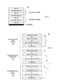
- FIG. 1 illustrates one example of a composite dielectric structure 10 configured in accordance with one embodiment of the present invention.
- composite dielectric structures formed on a substrate and in accordance with the present invention include alternating or repeating stacks of a doped dielectric layer for increasing capacitance (indicated as an LDL, ADL or CDL layer) and another layer for suppressing/blocking leakage current (indicated as an LBL layer).
- This composite dielectric structure 10 offers a high dielectric constant (k greater than that of HfO 2 and ZrO 2 ) while still maintaining low electrical leakage.
- the composite dielectric structure 10 is formed by building optimal LDL/ADL/CDL and LBL combination stacks using laminate, alloying or co-deposit strategies.
- a dopant or doping layer can be incorporated into a base dielectric layer (BDL) during any ALD process cycle and at any thickness from 0.5 nm to 200 nm.
- layer thickness may range from 0.1 nm to 100 nm.
- a composite dielectric structure 10 in accordance with the present invention may be symmetric or asymmetric in reference to the layer LDL/ADL/CDL (2) shown in FIG. 1 .
- a base dielectric layer may be formed by an ALD process with precisely controlled layer thickness.
- An ALD process incorporating selected dopants with desired electrical performance and precisely controlled doping concentrations into the BDL material may then form a doped dielectric layer.
- a doped dielectric layer with BDL and doping layer formed using successively applied films is referred to herein as a Laminate Dielectric Layer (LDL).
- a doped dielectric layer with BDL and dopant formed using an alternating base/dopant pulsing technique is referred to herein as an Alloy Dielectric Layer (ADL).
- a doped dielectric layer with BDL and dopant formed using a co-deposition process is referred to herein as a Co-deposit Dielectric Layer (CDL).
- a leakage blocking layer (LBL) may likewise be formed by an ALD process with precisely controlled layer thickness.
- a composite dielectric structure produced in accordance with the present invention provides a high-k doped dielectric material with desired electrical properties, including but not limited to:
- a composite dielectric structure made with an optimal design of LDL/ADL/CDL and LBL stacks promotes formation of tetragonal and cubic polymorphs that have higher dielectric constants at typical semiconductor processing temperatures.
- Post process annealing from 300° C. to 900° C. can further increase the dielectric constant.
- the charts shown in FIG. 2 provide examples of improved electrical performance with some designs of composite dielectric structures produced in accordance with the present invention annealed at temperatures between 300° C. and 900° C.
- dielectric constant increases of 10-100% can be achieved with the present composite dielectric structures, in contrast with base dielectric materials, such as ZrO 2 and HfO 2 .
- leakage current density reduction of as much as 50% can be accomplished with composite dielectric structures configured in accordance with the present invention, in comparison to base dielectric materials, such as ZrO 2 and HfO 2 .
- breakdown voltage (V bd ) enhancement of as much as 70% can be obtained with composite dielectric structures configured in accordance with the present invention, in comparison to base dielectric materials, such as ZrO 2 and HfO 2 .
- step coverage of more than 80% remains possible with a composite dielectric structure configured in accordance with the present invention.
- FIG. 3 illustrates an example of a process 20 for fabricating a composite dielectric structure in accordance with an embodiment of the present invention; in particular an ALD process for forming a base dielectric layer (BDL), a doped dielectric layer (LDL/ADL/CDL) using laminate, alloying and co-deposit schemes, and a leakage blocking layer (LBL).
- ALD ALD
- fabricating a composite dielectric structure is accomplished by formation of the desired stacks using various laminate, alloying or co-deposit strategies.
- the optimal design of LDL/ADL/CDL and LBL stacks produces the desired electrical performance.
- Process 20 thus includes sequential sub-processes for formation of a base dielectric layer (BDL) using BDL formation process 22 , a doped dielectric layer (LDL, ADL, CDL) using a doped dielectric layer formation process 24 , and a leakage blocking layer (LBL) using a leakage blocking layer formation process 26 .
- BDL base dielectric layer
- LDL doped dielectric layer
- LBL leakage blocking layer
- BDL formation process 22 includes repetition of a base precursor pulse, followed by a base precursor purge, and an oxidant (e.g., Ozone, O 2 , H 2 O) pulse, followed by a purge of the oxidant.
- Doped dielectric formation process 24 includes a dopant precursor pulse, followed by a dopant precursor purge, and an oxidant (e.g., Ozone, O 2 , H 2 O) pulse, followed by a purge of the oxidant.
- LBL formation process 26 includes a blocking precursor pulse, followed by a blocking precursor purge, and an oxidant (e.g., Ozone, O 2 , H 2 O) pulse, followed by a purge of the oxidant. As illustrated in FIG.
- the formation of composite dielectric stacks is achieved by successively depositing (e.g., as represented by loop D) doped dielectric layers (e.g., as represented by loop B) and leakage blocking layers (e.g., as represented by loop C).
- the numbers of ALD process cycles for base dielectric layer (A), doped dielectric layer (B), and leakage blocking layer (C) are dependent on the desired doping concentration, stack thickness, and electrical performance requirements for a composite dielectric structure.
- Optimal process repeatability can be achieved by accurate base dielectric thickness control, accurate dopant concentration and thickness control, and accurate blocking oxide thickness control.
- Process performance can be optimized through the use of desired process deposition rates, required process thickness uniformity within substrates, required process defect limitations, and preferred high process throughput.
- the present invention further concerns an atomic layer deposition (ALD) apparatus for fabricating a composite dielectric structure.
- FIG. 4 illustrates one example of such an ALD system 100 for fabricating BDL, LDL, ADL, CDL, and LBL materials.
- This configuration includes multiple precursor delivery lines, multiple oxidant delivery lines, multiple inert gas purging lines, a gas dispersion showerhead, and a heated susceptor for a substrate.
- the delivery of base precursors, dopant precursors, blocking precursors, oxidants and purge gasses is controlled by a controller 200 through the operation of valves (V) or other flow control devices within the delivery lines.
- V valves
- controller 200 may be a processor-based controller storing processor-executable instructions for performing the ALD processes discussed above with respect to FIG. 3 .
- An alternative ALD system 150 as in FIG. 5 , has one precursor vapour delivery system connected to multiple showerheads with corresponding susceptors.
- some embodiments of the ALD apparatus provide for delivery of up to five different precursors for fabricating a large combination of doped materials. Up to three different dopants can be incorporated into the BDL during the fabrication of desired composite dielectric structures, and precursors can be either liquids or solids dissolved in proper solvents.
- the ALD apparatus may also provide for delivery of up to three different oxidants for a variety of materials process and property optimization.
- the process chamber volume is adjustable, allowing for higher partial pressure and higher precursor dose concentration control during ALD process than would be the case if the volume were fixed.
- showerheads having a nozzle pattern that provides even distribution of precursor, oxidant and purge gas flows are used.
- a heated susceptor for heating a substrate provides stable control at typical semiconductor processing temperatures.
- one or more of the methods or processes described herein may be executable using various computer-based devices (e.g., controller 200 ).
- Such devices may include any electronic device capable of performing the actions described above (using suitable programming) and, where applicable, processing the information for display so as to properly convey the information.
- a processor may control the overall functions of the electronic device such as running applications and controlling peripherals (such as valves, mass flow controllers, and similar devices).
- the processor may use short-term memory to store operating instructions and to help in the execution of the operating instructions (e.g., such as the temporary storage of calculations and the like).
- the processor may also use non-transitory storage to store and read instructions, files, and other data that requires long term, non-volatile storage.
- FIG. 6 illustrates one example of a processor-based controller 200 suitable for use with an ALD apparatus configured in accordance with the present invention.
- Controller 200 includes main memory 201 and processor 202 communicatively coupled to one another over a bus 208 or other communication mechanism for communicating information.
- Main memory 201 may be any form of memory, such as a random access memory (RAM) or other dynamic storage device, for storing information and instructions 224 to be executed by processor 202 .
- Main memory 201 also may be used for storing temporary variables or other intermediate information during execution of instructions to be executed by processor 202 .
- Controller 200 further includes a read only memory (ROM) or other static storage device 206 coupled to the bus 208 for storing static information and instructions for the processor 202 .
- a storage device 216 having a machine readable storage medium (such as a hard disk) 222 , is provided and coupled to the bus 208 for storing information and instructions 224 .
- Controller 200 may also include a display 210 , for displaying information to a user.
- An input device 212 is coupled to the bus 208 for communicating information and command selections to the processor 202 .
- cursor controller 214 is Another type of user input device, such as a mouse, a trackball, etc., for use in communicating information and command selections to processor 202 and for controlling cursor movement on the display 210 , especially where a graphical user interface is used.
- processor 202 executes sequences of instructions contained in main memory 201 . Such instructions may be read into main memory 201 from another computer-readable medium, such as storage device 216 . Execution of the sequences of instructions contained in the main memory 201 causes the processor 202 to perform the process steps described above to effect the various ALD deposition sequences.
- main memory 201 may be read into main memory 201 from another computer-readable medium, such as storage device 216 . Execution of the sequences of instructions contained in the main memory 201 causes the processor 202 to perform the process steps described above to effect the various ALD deposition sequences.
- hard-wired circuitry may be used in place of or in combination with computer software instructions to implement the invention. Thus, embodiments of the invention are not limited to any specific combination of hardware circuitry and software.
- Controller 200 may also include a communication interface 220 coupled to the bus 208 .
- Communication interface 220 provides a two-way data communication channel for controller 200 via a network 226 .
- a signal generation device such as an alarm or buzzer may be included to signal alert or other conditions.
- the present invention provides a composite dielectric structure containing LDL, ADL, and/or CDL, as well as LBL layers, in which the LDL/ADL/CDL layers can have similar or different thickness, in which the thickness ranges from 0.1 nm-100 nm, and doping concentrations in each process loop (X or Y in FIG. 1 ).
- a dopant or doping layer can be incorporated into the BDL at any thickness from 0.5-200 nm and doping concentration ranges from 0.5-50% may be used.
- the doped layers can be formed by any one or more of LDL/ADL/CDL techniques in each process loop.
- LDL/ADL/CDL layer (2) is a central dielectric layer, having the most significant impact on the dielectric constant value of the composite dielectric structure.
- the number of LDL/ADL/CDL layer (1) and LBL (b) loops are selected to modulate the leakage current while still maintaining the dielectric constant for the structure.
- the number of LDL/ADL/CDL layer (3) and LBL (c) loops are selected to modulate the leakage current while still maintaining the dielectric constant for the structure.
- LBL (a), (b), (c) and (d) can have the same or different thicknesses, in which the thickness ranges from 0.1-100 nm.
- LBL (b) and (c) can have the same or different thicknesses in each X or Y loop, and LBL (a) and (d) can have the same or different thicknesses.
- the present composite dielectric structure may include base dielectric materials, dopants and leakage blocking materials, in which the base dielectric materials include ZrO 2 , HfO 2 , and any composite of ZrO 2 /HfO 2 mixtures.
- Dopants may include lanthanide metals; group III(B), IV(B) and V(B) metals; as well as oxides of such metals.
- Leakage blocking materials may include SiO 2 and Al 2 O 3 .
- the present composite dielectric structure may include doped dielectric layers (LDL, ADL and CDL), in which an LDL is formed by incorporating a doping layer into a base dielectric layer (BDL) using a laminate method, an ADL is formed by incorporating a dopant into a BDL using an alloying method, and a CDL is formed by pulsing a base material and a dopant together using a co-deposit method.
- LDL doped dielectric layers
- ADL is formed by incorporating a doping layer into a base dielectric layer (BDL) using a laminate method
- an ADL is formed by incorporating a dopant into a BDL using an alloying method
- a CDL is formed by pulsing a base material and a dopant together using a co-deposit method.
- a composite dielectric structure may include doped dielectric layers (e.g., LDL/ADL/CDL (1), (2) and (3) in FIG. 1 ), in which a single doping method (such as LDL, ADL or CDL) can be used throughout the entire structure; any combination of two or three doping methods (such as LDL+ADL, or LDL+CDL, or LDL+ADL+CDL) can be applied in each of the X and/or Y loops; and/or combined doping methods may be the same or different in each X and/or Y loop.
- doped dielectric layers e.g., LDL/ADL/CDL (1), (2) and (3) in FIG. 1
- a single doping method such as LDL, ADL or CDL
- any combination of two or three doping methods such as LDL+ADL, or LDL+CDL, or LDL+ADL+CDL
- doping methods may be the same or different in each X and/or Y loop.
- a composite dielectric structure can be symmetric or asymmetric with respect to a central layer thereof, such as LDL/ADL/CDL layer (2) in FIG. 1 , in which: the number of X loops of LDL/ADL/CDL (1) and LBL (b) layers can be from 0 to 500; the number of Y loops of LDL/ADL/CDL (3) and LBL (c) layers can be from 0 to 500; the number of X and Y loops can be the same or different; and/or the number of LBL (a) and (d) layers can be the same or different.
- ALD processes for fabricating composite dielectric structures containing BDL, LDL, ADL, CDL and LBL materials in accordance with embodiments of the present invention may include the combination (see loop D of FIG. 3 ) of doped dielectric depositions (B) (including LDL, ADL or CDL process) and leakage blocking depositions (C).
- the combined processes (D) may be designed to form films with desired doping concentrations, stack thicknesses, and electrical performances.
- BDL thickness may be controlled by the number of cycles of base dielectric process (A).
- Doped layer (LDL, ADL, and CDL) thickness may be controlled by the number of cycles of doped dielectric process (B).
- LBL thickness may be controlled by the number of cycles of leakage blocking process (C).
- metal pulse time and flow for base, doping and blocking precursors
- oxidant pulse time and flow for Ozone, O 2 , and H 2 O
- the deposition temperatures for forming these materials during ALD process may be between 100° C.-500° C., inclusive.
- a post-deposition processing step to “anneal” the stack for achieving targeted film properties may be used.
- a base metal precursor is pulsed into a chamber of an ALD apparatus with an Argon (or other neutral) carrier gas.
- Argon or other neutral carrier gas.
- excess base metal precursor is purged out and an oxidant (Ozone, O 2 or H 2 O) is pulsed into the chamber.
- the oxidant is purged out.
- a doping layer is incorporated into a base dielectric layer (BDL) using a laminating method.
- the thickness ratio of the doping layer and the BDL ranges from 0 to 50% to obtain the desired doping concentration.
- the laminating sequence of the doping layer into the BDL is selected to accomplish a desired doping layer with optimal electrical performance.
- the process sequence of the LDL formation includes pulsing a base metal precursor into a chamber of an ALD apparatus with an Argon (or other neutral) carrier gas.
- an ADL is formed by pulsing (once or multiple times) of a base metal followed by a dopant before the injection of oxidant into the chamber.
- the thickness ratio of the doped layer and the BDL ranges from 0 to 50% to obtain the desired doping concentration. Doping concentration can also be controlled by the amount of dopant injected during each ALD cycle.
- the alloying sequence of the dopant into the BDL is selected to accomplish a desired doping layer with optimal electrical performance.
- One such example of a process for ADL layer formation includes pulsing the base metal precursor into the chamber with Argon (or other neutral) carrier gas.
- a CDL is formed by injecting base metal and dopant simultaneously before the injection of oxidant into the chamber.
- Doping concentration may be controlled by varying the ratio of metal and dopant precursors used in the pulses.
- Doping concentration may also be controlled by the thickness ratio of the co-deposited layer and the BDL, ranging from 0-50%.
- the co-depositing sequence of the metal/dopant into the BDL is selected to accomplish a desired doping layer with optimal electrical performance.
- An example of a process sequence for CDL formation involves pulsing base metal and dopant precursors into a chamber together with Argon (or other neutral) carrier gas.
- a leakage block precursor is pulsed into the chamber with Argon (or other) carrier gas.
- Argon or other carrier gas.
- excess leakage blocking precursor is purged out and an oxidant (Ozone, O 2 or H 2 O) is pulsed into the chamber.
- the oxidant is purged out of the chamber.
- the composite dielectric structure of the present invention can be crystallographically stabilized in the tetragonal or/and cubic phases, which have higher dielectric constants upon post-process annealing.
- the structure can be annealed under inert gases, such as Argon, N 2 or forming gas N 2 /H 2 , or other environments.
- the structure can be annealed at temperatures between 300-900° C., inclusive.
- the structure can also be photo irradiated by infrared, visible, or ultraviolet light, and/or can be treated by electron and ion irradiation.
- An apparatus suitable for fabricating a composite dielectric structure containing BDL, LDL, ADL, CDL and LBL materials using ALD techniques may include a precursor vapour delivery system (e.g., under the control of a suitably programmed processor-based controller) and a process chamber.
- the process chamber may include one or more identical reactor chambers, each reactor chamber having a showerhead and a susceptor (preferably heated) for supporting a substrate.
- a multi-reactor chamber may have multiple identical showerheads, susceptors, and process volumes.
- Each reactor may be isolated from the others by dynamic laminar inert gas flows to facilitate fast purging and short ALD cycle times.
- the laminar inert gas flows may be between 0.1 L to 10 L.
- the precursor vapour delivery system is connected to the showerhead(s) as is an oxidant delivery system, but the gas delivery lines of the oxidant delivery system are separated from the precursor delivery lines.
- Various inert gas lines facilitate inert gas delivery for process gas purging, precursor vapour carriers, and reactor isolating gas flows.
- a showerhead may have two separate gas flow paths, one for precursors and another for oxidants.
- the showerhead is preferably designed to provide evenly distributed precursors, oxidants, and inert gases.
- precursor vapour flow is adjustable to obtain the optimal deposition uniformity; for example, adjustable between approximately 0.1 to 10 L.
- Oxidant flow may also be adjustable between approximately 0.1 to 10 L to provide the optimal film quality.
- showerhead temperatures are preferably controlled to be between 100-300° C., inclusive.
- the susceptor is used to control the substrate process temperature needed for typical semiconductor devices between 100 and 600° C.
- a substrate is placed on the susceptor and the susceptor is moved vertically up and down to adjust the distance between the substrate and the showerhead.
- the precursor vapour delivery system can supply up to five different precursor sources, including base metals, dopants and leakage blocking precursors.
- Each precursor source can be operated independently of the others and each precursor source can be operated in synchronization with one or more other precursor sources (e.g., through programmatic control of controller 200 ).
- the abundant variety of precursor sources allow to pulse as many as three doping materials into the chamber at the same time for creating the LDL, ADL, and CDL materials and the combined stacks with desired electrical performance.
- the ALD system may also include a precursor vaporizer for vapour delivery into the chamber.
- the vaporizer can effectively transform the liquid precursors or solid precursors dissolved in proper solvents to high concentration precursor vapours.
- the vaporizer is heated and the temperature can be adjusted (based on precursor's vapour pressure) between 100 to 300° C., inclusive.
- Vaporized precursor vapour is carried into the reactor via inert carrier gas, which flow is approximately between 0.1 L to 10 L, inclusive.
- the vapour delivery line for transferring the precursor vapour to the chamber is also heated to be between 100 to 300° C., inclusive.
- the oxidant delivery system is configured to permit oxidants, e.g., ozone in desired concentration or oxygen, to be delivered into the reactor through the showerhead.
- Ozone concentrations may be selected dependent on the requirements for the film properties and substrate tolerance, for example between 10 to 500 g/m 3 .
- Ozone and oxygen flows may range from 0.1 to 50 L, inclusive.
- Oxidant, H 2 O vapour at controlled temperature can also be delivered into the reactor through the showerhead.
- H 2 O vapour temperature is preferably controlled to be between room temperature and 100° C., inclusive.
- the ALD system also includes multiple inert gas lines. Inert gas is used for metal and oxidant purging during ALD process, to carry precursor vapours into the reactors, and for creating gas flow curtains around the reactors of a multi-reactor chamber for mutual isolation.
- Method examples described herein can be machine or computer-implemented at least in part. Some examples can include a computer-readable medium or machine-readable medium encoded with instructions operable to configure an electronic device to perform methods as described in the above examples.
- An implementation of such methods can include code, such as microcode, assembly language code, a higher-level language code, or the like. Such code can include computer readable instructions for performing various methods.
- the code may form portions of computer program products.
- the code can be stored on one or more non-transitory, or non-volatile tangible computer-readable media, and may be loaded into volatile media during execution or at other times (e.g., during a transfer between storage devices, etc.).
- tangible computer-readable media can include, but are not limited to, hard disks, removable magnetic disks, removable optical disks (e.g., compact disks and digital video disks), magnetic cassettes, memory cards or sticks, read only memories (ROMs), flash memories or other solid state devices (SSDs) and the like.
- hard disks removable magnetic disks, removable optical disks (e.g., compact disks and digital video disks), magnetic cassettes, memory cards or sticks, read only memories (ROMs), flash memories or other solid state devices (SSDs) and the like.
Landscapes
- Engineering & Computer Science (AREA)
- Chemical & Material Sciences (AREA)
- Microelectronics & Electronic Packaging (AREA)
- Power Engineering (AREA)
- Condensed Matter Physics & Semiconductors (AREA)
- General Physics & Mathematics (AREA)
- Computer Hardware Design (AREA)
- Physics & Mathematics (AREA)
- Manufacturing & Machinery (AREA)
- Chemical Kinetics & Catalysis (AREA)
- General Chemical & Material Sciences (AREA)
- Organic Chemistry (AREA)
- Materials Engineering (AREA)
- Mechanical Engineering (AREA)
- Metallurgy (AREA)
- Ceramic Engineering (AREA)
- Inorganic Chemistry (AREA)
- Crystallography & Structural Chemistry (AREA)
- Chemical Vapour Deposition (AREA)
- Formation Of Insulating Films (AREA)
- Semiconductor Memories (AREA)
- Insulated Gate Type Field-Effect Transistor (AREA)
Abstract
Description
-
- A higher dielectric constant value than that of HfO2 or ZrO2 alone;
- An equivalent or lower leakage current than that of HfO2 or ZrO2 alone;
- An equivalent or increased breakdown voltage than that of HfO2 or ZrO2 alone; and
- An equivalent or improved step coverage than that of HfO2 or ZrO2 alone.
Claims (18)
Priority Applications (1)
| Application Number | Priority Date | Filing Date | Title |
|---|---|---|---|
| US14/553,436 US9564329B2 (en) | 2013-12-01 | 2014-11-25 | Method and apparatus for fabricating dielectric structures |
Applications Claiming Priority (2)
| Application Number | Priority Date | Filing Date | Title |
|---|---|---|---|
| US201361910383P | 2013-12-01 | 2013-12-01 | |
| US14/553,436 US9564329B2 (en) | 2013-12-01 | 2014-11-25 | Method and apparatus for fabricating dielectric structures |
Publications (2)
| Publication Number | Publication Date |
|---|---|
| US20150155157A1 US20150155157A1 (en) | 2015-06-04 |
| US9564329B2 true US9564329B2 (en) | 2017-02-07 |
Family
ID=53265915
Family Applications (1)
| Application Number | Title | Priority Date | Filing Date |
|---|---|---|---|
| US14/553,436 Active US9564329B2 (en) | 2013-12-01 | 2014-11-25 | Method and apparatus for fabricating dielectric structures |
Country Status (4)
| Country | Link |
|---|---|
| US (1) | US9564329B2 (en) |
| JP (2) | JP6616070B2 (en) |
| KR (2) | KR102181679B1 (en) |
| TW (1) | TWI651755B (en) |
Families Citing this family (10)
| Publication number | Priority date | Publication date | Assignee | Title |
|---|---|---|---|---|
| US9388494B2 (en) | 2012-06-25 | 2016-07-12 | Novellus Systems, Inc. | Suppression of parasitic deposition in a substrate processing system by suppressing precursor flow and plasma outside of substrate region |
| US9617638B2 (en) | 2014-07-30 | 2017-04-11 | Lam Research Corporation | Methods and apparatuses for showerhead backside parasitic plasma suppression in a secondary purge enabled ALD system |
| US9508547B1 (en) * | 2015-08-17 | 2016-11-29 | Lam Research Corporation | Composition-matched curtain gas mixtures for edge uniformity modulation in large-volume ALD reactors |
| US9738977B1 (en) | 2016-06-17 | 2017-08-22 | Lam Research Corporation | Showerhead curtain gas method and system for film profile modulation |
| KR102369676B1 (en) | 2017-04-10 | 2022-03-04 | 삼성디스플레이 주식회사 | Apparatus and method for manufacturing a display apparatus |
| TWI838267B (en) * | 2018-06-21 | 2024-04-01 | 美商應用材料股份有限公司 | Thin films and methods of depositing thin films |
| CN114402416A (en) | 2019-07-17 | 2022-04-26 | 朗姆研究公司 | Oxidation profile tuning for substrate processing |
| US20230420491A1 (en) * | 2022-06-28 | 2023-12-28 | International Business Machines Corporation | Ferroelectric Film with Buffer Layers for Improved Reliability of Metal-Insulator-Metal Capacitor |
| KR102637458B1 (en) | 2023-04-11 | 2024-02-16 | 현진인터내셔널 주식회사 | Eco-friendly heat insulation deck with improved durability and antifouling performance and its manufacturing method |
| CN116875961A (en) * | 2023-09-01 | 2023-10-13 | 上海陛通半导体能源科技股份有限公司 | Atomic layer deposition apparatus |
Citations (18)
| Publication number | Priority date | Publication date | Assignee | Title |
|---|---|---|---|---|
| US20020042165A1 (en) * | 2000-04-14 | 2002-04-11 | Matti Putkonen | Process for producing oxide thin films |
| US20040043557A1 (en) * | 2000-10-10 | 2004-03-04 | Haukka Suvi P. | Methods for making a dielectric stack in an integrated circuit |
| US20040245602A1 (en) * | 2003-05-21 | 2004-12-09 | Kim Sun Jung | Method of fabricating metal-insulator-metal capacitor (MIM) using lanthanide-doped HfO2 |
| US20050239298A1 (en) * | 2004-04-27 | 2005-10-27 | Commissariat A L'energie Atomique | Process for deposition of a thin layer on an oxidized layer of a substrate |
| US20080122044A1 (en) * | 2006-11-24 | 2008-05-29 | Samsung Electronics Co., Ltd. | Method manufacturing capacitor dielectric |
| US20080233288A1 (en) * | 2007-03-20 | 2008-09-25 | Tokyo Electron Limited | Method of forming crystallographically stabilized doped hafnium zirconium based films |
| US20090189235A1 (en) * | 2007-05-07 | 2009-07-30 | Sony Corporation | Solid-state imaging device, manufacturing method for the same, and imaging apparatus |
| US20100091428A1 (en) * | 2008-10-13 | 2010-04-15 | Kwan-Soo Kim | Insulator, capacitor with the same and fabrication method thereof, and method for fabricating semionductor device |
| US20100164064A1 (en) * | 2008-12-31 | 2010-07-01 | Hyun Dong Kim | Capacitor and Method for Manufacturing the Same |
| US7754618B2 (en) | 2005-02-10 | 2010-07-13 | Micron Technology, Inc. | Method of forming an apparatus having a dielectric containing cerium oxide and aluminum oxide |
| US7833914B2 (en) | 2007-04-27 | 2010-11-16 | Micron Technology, Inc. | Capacitors and methods with praseodymium oxide insulators |
| US20110014770A1 (en) * | 2009-07-14 | 2011-01-20 | Samsung Electronics Co., Ltd. | Methods of forming a dielectric thin film of a semiconductor device and methods of manufacturing a capacitor having the same |
| US20120082283A1 (en) * | 2010-09-30 | 2012-04-05 | Liviu Popa-Simil | Method of using micro-nano-hetro structures to make radiation detection systems and devices with applications |
| US20120127629A1 (en) | 2009-04-16 | 2012-05-24 | Advanced Technology Materials, Inc. | DOPED ZrO2 CAPACITOR MATERIALS AND STRUCTURES |
| US20120181660A1 (en) * | 2011-01-14 | 2012-07-19 | Elpida Memory, Inc. | Semiconductor device |
| US20130143379A1 (en) * | 2011-12-05 | 2013-06-06 | Elpida Memory, Inc. | Leakage reduction in dram mim capacitors |
| US20130200491A1 (en) * | 2012-02-06 | 2013-08-08 | Tokyo Electron Limited | Method of manufacturing capacitor, capacitor and method of forming dielectric film for use in capacitor |
| US20150035085A1 (en) * | 2013-08-02 | 2015-02-05 | Intermolecular Inc. | Doped High-k Dielectrics and Methods for Forming the Same |
Family Cites Families (10)
| Publication number | Priority date | Publication date | Assignee | Title |
|---|---|---|---|---|
| JPH11214127A (en) * | 1998-01-21 | 1999-08-06 | Riken Corp | Heater device and manufacture of the same |
| JP2007266438A (en) * | 2006-03-29 | 2007-10-11 | Hitachi Ltd | Semiconductor memory device |
| JP2008112956A (en) * | 2006-08-03 | 2008-05-15 | Sony Corp | Capacitor, method of producing same, semiconductor device, and liquid crystal display device |
| US7723771B2 (en) * | 2007-03-30 | 2010-05-25 | Qimonda Ag | Zirconium oxide based capacitor and process to manufacture the same |
| KR101541544B1 (en) * | 2007-12-26 | 2015-08-03 | 소니 주식회사 | Solid-state imaging device, manufacturing method for the same, and imaging apparatus |
| TWI467045B (en) * | 2008-05-23 | 2015-01-01 | Sigma Aldrich Co | High-k dielectric films and methods of producing high-k dielectric films using cerium-based precursors |
| JP2011204751A (en) * | 2010-03-24 | 2011-10-13 | Elpida Memory Inc | Method of manufacturing semiconductor device |
| JP5587716B2 (en) * | 2010-09-27 | 2014-09-10 | マイクロンメモリジャパン株式会社 | Semiconductor device, manufacturing method thereof, and adsorption site blocking atomic layer deposition method |
| JP2013058559A (en) * | 2011-09-07 | 2013-03-28 | Tokyo Electron Ltd | Manufacturing method of semiconductor device and substrate processing system |
| KR101475996B1 (en) * | 2012-02-29 | 2014-12-24 | 매그나칩 반도체 유한회사 | Insulator, capacitor with the same and fabricating method thereof, and method for fabricating semiconductor device |
-
2014
- 2014-11-21 JP JP2014236852A patent/JP6616070B2/en active Active
- 2014-11-25 US US14/553,436 patent/US9564329B2/en active Active
- 2014-12-01 TW TW103141656A patent/TWI651755B/en active
- 2014-12-01 KR KR1020140169718A patent/KR102181679B1/en active IP Right Grant
-
2019
- 2019-08-14 JP JP2019148890A patent/JP6906572B2/en active Active
-
2020
- 2020-11-16 KR KR1020200153129A patent/KR102393908B1/en active IP Right Grant
Patent Citations (20)
| Publication number | Priority date | Publication date | Assignee | Title |
|---|---|---|---|---|
| US6548424B2 (en) * | 2000-04-14 | 2003-04-15 | Asm Microchemistry Oy | Process for producing oxide thin films |
| US20020042165A1 (en) * | 2000-04-14 | 2002-04-11 | Matti Putkonen | Process for producing oxide thin films |
| US20040043557A1 (en) * | 2000-10-10 | 2004-03-04 | Haukka Suvi P. | Methods for making a dielectric stack in an integrated circuit |
| US20040245602A1 (en) * | 2003-05-21 | 2004-12-09 | Kim Sun Jung | Method of fabricating metal-insulator-metal capacitor (MIM) using lanthanide-doped HfO2 |
| US20050239298A1 (en) * | 2004-04-27 | 2005-10-27 | Commissariat A L'energie Atomique | Process for deposition of a thin layer on an oxidized layer of a substrate |
| US7754618B2 (en) | 2005-02-10 | 2010-07-13 | Micron Technology, Inc. | Method of forming an apparatus having a dielectric containing cerium oxide and aluminum oxide |
| US20080122044A1 (en) * | 2006-11-24 | 2008-05-29 | Samsung Electronics Co., Ltd. | Method manufacturing capacitor dielectric |
| US20080233288A1 (en) * | 2007-03-20 | 2008-09-25 | Tokyo Electron Limited | Method of forming crystallographically stabilized doped hafnium zirconium based films |
| US7833913B2 (en) | 2007-03-20 | 2010-11-16 | Tokyo Electron Limited | Method of forming crystallographically stabilized doped hafnium zirconium based films |
| US7833914B2 (en) | 2007-04-27 | 2010-11-16 | Micron Technology, Inc. | Capacitors and methods with praseodymium oxide insulators |
| US20090189235A1 (en) * | 2007-05-07 | 2009-07-30 | Sony Corporation | Solid-state imaging device, manufacturing method for the same, and imaging apparatus |
| US20100091428A1 (en) * | 2008-10-13 | 2010-04-15 | Kwan-Soo Kim | Insulator, capacitor with the same and fabrication method thereof, and method for fabricating semionductor device |
| US20100164064A1 (en) * | 2008-12-31 | 2010-07-01 | Hyun Dong Kim | Capacitor and Method for Manufacturing the Same |
| US20120127629A1 (en) | 2009-04-16 | 2012-05-24 | Advanced Technology Materials, Inc. | DOPED ZrO2 CAPACITOR MATERIALS AND STRUCTURES |
| US20110014770A1 (en) * | 2009-07-14 | 2011-01-20 | Samsung Electronics Co., Ltd. | Methods of forming a dielectric thin film of a semiconductor device and methods of manufacturing a capacitor having the same |
| US20120082283A1 (en) * | 2010-09-30 | 2012-04-05 | Liviu Popa-Simil | Method of using micro-nano-hetro structures to make radiation detection systems and devices with applications |
| US20120181660A1 (en) * | 2011-01-14 | 2012-07-19 | Elpida Memory, Inc. | Semiconductor device |
| US20130143379A1 (en) * | 2011-12-05 | 2013-06-06 | Elpida Memory, Inc. | Leakage reduction in dram mim capacitors |
| US20130200491A1 (en) * | 2012-02-06 | 2013-08-08 | Tokyo Electron Limited | Method of manufacturing capacitor, capacitor and method of forming dielectric film for use in capacitor |
| US20150035085A1 (en) * | 2013-08-02 | 2015-02-05 | Intermolecular Inc. | Doped High-k Dielectrics and Methods for Forming the Same |
Also Published As
| Publication number | Publication date |
|---|---|
| TW201539525A (en) | 2015-10-16 |
| TWI651755B (en) | 2019-02-21 |
| JP6616070B2 (en) | 2019-12-04 |
| KR20150063939A (en) | 2015-06-10 |
| JP6906572B2 (en) | 2021-07-21 |
| US20150155157A1 (en) | 2015-06-04 |
| JP2015106713A (en) | 2015-06-08 |
| JP2020004985A (en) | 2020-01-09 |
| KR102393908B1 (en) | 2022-05-02 |
| KR102181679B1 (en) | 2020-11-24 |
| KR20200133195A (en) | 2020-11-26 |
Similar Documents
| Publication | Publication Date | Title |
|---|---|---|
| KR102393908B1 (en) | Method and apparatus for fabricating dielectric structures | |
| KR100716654B1 (en) | Method for manufacturing tetragonal zirconium oxide and method for manufacturing capacitor with the same | |
| KR102693828B1 (en) | Method for forming silicon oxide cap layer for solid state diffusion process | |
| JP5013662B2 (en) | Capacitor and manufacturing method thereof | |
| US20090011145A1 (en) | Method of Manufacturing Vanadium Oxide Thin Film | |
| US7888726B2 (en) | Capacitor for semiconductor device | |
| KR20070050163A (en) | Capacitor and method of manufacturing the same | |
| DE112010001364T5 (en) | A method of forming a high k gate stack with reduced effective oxide thickness | |
| KR20140040641A (en) | Method of manufacturing semiconductor device, substrate processing method and apparatus, non-transitory computer readable recording medium, and semiconductor device | |
| JPH06275548A (en) | Formation of cvd thin film | |
| Cho et al. | Atomic layer deposition of TiO 2 using titanium isopropoxide and H 2 O: operational principle of equipment and parameter setting | |
| KR100663352B1 (en) | Method of manufacturing silicon doped metal oxide layer using atomic layer deposition technique | |
| KR100780650B1 (en) | Capacitor in semiconductor device and method for using the same | |
| JP5385723B2 (en) | Semiconductor device manufacturing method and semiconductor device | |
| KR100744026B1 (en) | Method for manufacturing flash memory device | |
| KR100770276B1 (en) | Method of forming mim capacitor in semiconductor device | |
| KR100971413B1 (en) | Capacitor in semiconductor device and method for manufacturing the same | |
| KR101752060B1 (en) | Electric Device for MIM Capacitor having Enhanced electrical characteristics and Manufacturing Method thereof | |
| KR101152390B1 (en) | Dielectric layer in capacitor and fabricating using the same and capacitor in semiconductor device and fabricating using the same | |
| US6989338B2 (en) | Method for forming a multi-layered structure of a semiconductor device and methods for forming a capacitor and a gate insulation layer using the multi-layered structure | |
| KR20160112348A (en) | Metal oxide thin film having massive crystaline particles and manufacturing method thereof | |
| WO2006026018A2 (en) | Atomic layer deposition of high quality high-k transition metal and rare earth oxides | |
| KR20160042404A (en) | Multi and asymmetric complex thin film using atomic layer deposition and method for manufacturing thereof | |
| TW202349463A (en) | Bilayer stack for a ferroelectric tunnel junction and method of forming | |
| KR20070049927A (en) | Titanium-aluminum dielectric film and preparing method of the same |
Legal Events
| Date | Code | Title | Description |
|---|---|---|---|
| AS | Assignment |
Owner name: AIXTRON, SE, GERMANY Free format text: ASSIGNMENT OF ASSIGNORS INTEREST;ASSIGNORS:SONG, KAY;LU, BRIAN;LI, MINGHANG;SIGNING DATES FROM 20141202 TO 20150113;REEL/FRAME:035581/0058 |
|
| STCF | Information on status: patent grant |
Free format text: PATENTED CASE |
|
| AS | Assignment |
Owner name: EUGENE TECHNOLOGY, INC., CALIFORNIA Free format text: ASSIGNMENT OF ASSIGNORS INTEREST;ASSIGNOR:AIXTRON, INC.;REEL/FRAME:044767/0357 Effective date: 20171115 Owner name: EUGENUS, INC., CALIFORNIA Free format text: CHANGE OF NAME;ASSIGNOR:EUGENE TECHNOLOGY, INC.;REEL/FRAME:045444/0996 Effective date: 20171116 |
|
| AS | Assignment |
Owner name: EUGENUS, INC., CALIFORNIA Free format text: ASSIGNMENT OF ASSIGNORS INTEREST;ASSIGNOR:AIXTRON SE;REEL/FRAME:045538/0863 Effective date: 20180320 |
|
| MAFP | Maintenance fee payment |
Free format text: PAYMENT OF MAINTENANCE FEE, 4TH YEAR, LARGE ENTITY (ORIGINAL EVENT CODE: M1551); ENTITY STATUS OF PATENT OWNER: LARGE ENTITY Year of fee payment: 4 |
|
| FEPP | Fee payment procedure |
Free format text: ENTITY STATUS SET TO SMALL (ORIGINAL EVENT CODE: SMAL); ENTITY STATUS OF PATENT OWNER: SMALL ENTITY |