US9559280B2 - Thermoelectric conversion device - Google Patents

Thermoelectric conversion device Download PDF

Info

Publication number
US9559280B2
US9559280B2 US14/635,764 US201514635764A US9559280B2 US 9559280 B2 US9559280 B2 US 9559280B2 US 201514635764 A US201514635764 A US 201514635764A US 9559280 B2 US9559280 B2 US 9559280B2
Authority
US
United States
Prior art keywords
thermoelectric conversion
heusler alloy
alloy film
conversion device
voltage
Prior art date
Legal status (The legal status is an assumption and is not a legal conclusion. Google has not performed a legal analysis and makes no representation as to the accuracy of the status listed.)
Expired - Fee Related, expires
Application number
US14/635,764
Other versions
US20150280095A1 (en
Inventor
Jun Hayakawa
Shin Yabuuchi
Masakuni Okamoto
Yosuke Kurosaki
Akinori Nishide
Current Assignee (The listed assignees may be inaccurate. Google has not performed a legal analysis and makes no representation or warranty as to the accuracy of the list.)
Hitachi Ltd
Original Assignee
Hitachi Ltd
Priority date (The priority date is an assumption and is not a legal conclusion. Google has not performed a legal analysis and makes no representation as to the accuracy of the date listed.)
Filing date
Publication date
Application filed by Hitachi Ltd filed Critical Hitachi Ltd
Priority to US14/635,764 priority Critical patent/US9559280B2/en
Publication of US20150280095A1 publication Critical patent/US20150280095A1/en
Application granted granted Critical
Publication of US9559280B2 publication Critical patent/US9559280B2/en
Expired - Fee Related legal-status Critical Current
Adjusted expiration legal-status Critical

Links

Images

Classifications

    • H01L35/20
    • H01L35/12
    • H01L35/32
    • H01L37/00
    • HELECTRICITY
    • H10SEMICONDUCTOR DEVICES; ELECTRIC SOLID-STATE DEVICES NOT OTHERWISE PROVIDED FOR
    • H10NELECTRIC SOLID-STATE DEVICES NOT OTHERWISE PROVIDED FOR
    • H10N10/00Thermoelectric devices comprising a junction of dissimilar materials, i.e. devices exhibiting Seebeck or Peltier effects
    • H10N10/10Thermoelectric devices comprising a junction of dissimilar materials, i.e. devices exhibiting Seebeck or Peltier effects operating with only the Peltier or Seebeck effects
    • H10N10/17Thermoelectric devices comprising a junction of dissimilar materials, i.e. devices exhibiting Seebeck or Peltier effects operating with only the Peltier or Seebeck effects characterised by the structure or configuration of the cell or thermocouple forming the device
    • HELECTRICITY
    • H10SEMICONDUCTOR DEVICES; ELECTRIC SOLID-STATE DEVICES NOT OTHERWISE PROVIDED FOR
    • H10NELECTRIC SOLID-STATE DEVICES NOT OTHERWISE PROVIDED FOR
    • H10N10/00Thermoelectric devices comprising a junction of dissimilar materials, i.e. devices exhibiting Seebeck or Peltier effects
    • H10N10/80Constructional details
    • H10N10/85Thermoelectric active materials
    • H10N10/851Thermoelectric active materials comprising inorganic compositions
    • H10N10/854Thermoelectric active materials comprising inorganic compositions comprising only metals
    • HELECTRICITY
    • H10SEMICONDUCTOR DEVICES; ELECTRIC SOLID-STATE DEVICES NOT OTHERWISE PROVIDED FOR
    • H10NELECTRIC SOLID-STATE DEVICES NOT OTHERWISE PROVIDED FOR
    • H10N15/00Thermoelectric devices without a junction of dissimilar materials; Thermomagnetic devices, e.g. using the Nernst-Ettingshausen effect

Definitions

  • the present invention relates to a thermoelectric conversion device and particularly to a thermoelectric conversion device including an electrode for electric field to thermoelectric conversion material.
  • thermal conversion Conversion of thermal energy into electric energy using Seebeck effect on a substance is called thermal conversion, and a device capable of the thermal conversion is a thermal conversion device.
  • a material used in the thermal conversion device is called a thermal conversion material.
  • thermoelectric conversion device The performance index necessary for realizing the thermoelectric conversion device is defined by ZT (T is a temperature). Generally a ZT equal to or more than one is required, and a ZT equal to or more than two is required partially.
  • JP 2009-117430 A discloses a thermoelectric device including a pair of a source electrode S and a drain electrode D for taking out an electromotive force according to a thermal gradient generated in a semiconductor A having a carrier density equal to or smaller than 10 22 /cm 3 and for generating the thermal gradient in the semiconductor A by conducting a current, and a gate electrode G for applying an electric field in the vertical direction to a conduction direction of the current between the source electrode S and the drain electrode D.
  • a voltage is applied to the gate electrode G, a carrier density on a surface of the semiconductor A just under the gate electrode G varies.
  • thermoelectric conversion device having an electric conductivity and a Seebeck coefficient S greater than conventional thermoelectric conversion devices.
  • A a single or a plurality of elements belonging to any of seventh to tenth groups of fourth to sixth periods in the periodic table of element.
  • B a single or a plurality of elements belonging to any of fourth to sixth groups of fourth to sixth periods in the periodic table of element.
  • FIG. 1 is a cross section view of an example of a thermoelectric conversion device according to a first embodiment of the present invention
  • FIG. 2 is a cross section view of a configuration example of a thermoelectric conversion device according to a second embodiment of the present invention
  • FIG. 3 is a cross section view of a configuration example of a thermoelectric conversion device according to a third embodiment of the present invention.
  • FIG. 4 is a cross section view of a configuration example of a thermoelectric conversion device according to a fourth embodiment of the present invention.
  • FIG. 5 is a table of elements to illustrate elements forming thermoelectric conversion material according to the present invention.
  • FIG. 6A to 6D are charts of performance indexes Z illustrating increase quantities with respect to applied voltages to the thermoelectric conversion devices according to the present invention
  • FIG. 7 is a table of optimum applied voltage values of the thermoelectric conversion devices regarding a typical Heusler alloy film material
  • FIGS. 8A to 8C are charts illustrating a principle of increase in the performance index Z of the thermoelectric devices according to the present invention.
  • FIG. 9 shows an example of an array of the thermoelectric conversion device according to the present invention.
  • FIG. 10 shows an example of an array of the thermoelectric conversion device according to the present invention.
  • FIG. 11 is a circuit diagram of an example of an arrangement of the thermoelectric conversion devices according to the present invention.
  • FIG. 1 is a cross section view of an example of a thermoelectric conversion device (part) according to the present invention.
  • the thermoelectric conversion device includes a Heusler alloy film 100 laminated on a substrate 200 having a small thermal conductivity through a buffer layer 201 and a seed layer 202 , and a pair of electrodes 501 and 502 .
  • An electromotive force (thermal electromotive force) generated by a thermal gradient in the Heusler alloy film 100 is taken out (is outputted as a voltage V) by a pair of the electrodes 501 and 502 disposed at a predetermined distance D therebetween as shown in FIG. 1 .
  • the Heusler alloy film 100 has a crystal structure of B 2 or L 21 indicated in an A 2 BC notation. Elements used in A, B, and C in the A 2 BC notation are as follows:
  • A a single element or a plurality of elements belonging to any of seventh to tenth groups of fourth to sixth periods in the periodic table.
  • C a single element or a plurality of elements belonging to any of thirteenth to fourteenth groups of third to sixth periods of the periodic table.
  • Ta, Ru, Ti, or Zr, etc. is used for the buffer layer 201 .
  • a material having a body-centered cubic (bcc) structure such as V, Cr, and W or MgO, MgZnO, etc. is preferably used.
  • Adopting such materials for the seed layer 202 enables formation of the Heusler alloy film having the B 2 or L 2 1 structure.
  • the Heusler alloy film having the B 2 or L 21 structure can be formed stably by heating the substrate at a temperature equal to or higher than 300° C. or a thermal process at a temperature equal to or higher than 300° C. while the Heusler alloy film is formed.
  • Fe 2 TiSn having the L 21 structure provides an extremely great performance index Z.
  • FIG. 2 shows a configuration in which a protection film 203 is laminated on the Heusler alloy film 100 of the thermoelectric conversion device shown in FIG. 1 .
  • Use of the protection film can prevent the Heusler alloy film 100 from deterioration.
  • a material having a high melting point and a low thermal conductivity such as Ta or V are usable.
  • A a single element or a plurality of elements in the seventh to tenth groups of the fourth to sixth periods in the periodic table, and the crystal structure is formed with the single element or these more than one elements.
  • C a single element or a plurality of elements in the thirteenth to fourteenth groups of the third to sixth periods in the periodic table, and the crystal structure is formed with the single element or this more than one element.
  • FIGS. 6A to 6D show increase quantities of the performance index Z of these Heusler alloy materials with respect to the voltage Vg applied to the electrodes 503 . In each of the charts in FIGS. 6A to 6D , the performance index Z rapidly increases from voltages indicated by arrows.
  • FIG. 7 shows a table to show optimum application voltages of the four kinds of materials described above. From this table, it is found that in Fe 2 TiSn, the increase in the performance index Z is possible at a low voltage of ⁇ 0.1V.
  • FIG. 8A shows a typical density of state of the Heusler metal film. The density of state indicates the number of electrons for each energy state.
  • a vertical axis in FIG. 8A represents energy, and the horizontal axis represents the density of states of electrons (DOS).
  • Fermi energy (E F ) indicated in FIG. 8A represents an energy of electrons are caused to be finally occupied in a band while electrons are caused to be occupied in bands from a lower energy band.
  • an energy EF indicated with a solid line shifts to an energy EF indicated by broken lines from the state in which the voltage Vg is not applied to the state in which the voltage Vg is applied.
  • the Seebeck index S defining the performance index Z is proportional to an inclination of the energy of the density of state DOS
  • the electric conductivity ⁇ is proportional to the density of state DOS
  • an appropriate variation of the voltage Vg provides a state in which increase in both of the Seebeck index S and the electric conductivity ⁇ are allowed.
  • FIGS. 8A and 8C show Vg dependencies of the electric conductivity ⁇ and the Seebeck coefficient Vg of the Heusler structure having the density of state shown in FIG. 8A .
  • FIGS. 8B and 8C it becomes possible that the electric conductivity ⁇ increases with respect to the voltage Vg and the Seebeck coefficient S has a local maximum at a certain Vg value.
  • FIG. 4 shows an example of the thermoelectric conversion device allowing the electromotive force generated by the Heusler alloy film 100 itself to be applied to the electrode 503 through a line 506 in addition to the configuration shown in FIG. 3 .
  • This configuration provides a thermoelectric conversion device which does not require external power to be consumed because an external power supply is not used. Because the electromotive force generated by the thermoelectric conversion device itself has a level necessary for the application voltage shown in FIG. 7 , it is possible that the performance index Z can be increased by the electromotive force generated by the thermoelectric conversion device itself.
  • FIG. 9 shows a configuration of a thermoelectric conversion device in which a plurality of single thermoelectric conversion devices shown in FIG. 3 are disposed in an array, and the electrodes 501 and 502 have a shared connection among a plurality of the thermoelectric conversion devices.
  • This configuration can increase the electromotive force which is taken out from a plurality of the thermoelectric conversion devices.
  • the electrode 503 and the electrode 504 are disposed so as to cross each other above the other part of the thermoelectric conversion device, and voltages applied to the electrodes 503 and the electrode 504 are controlled to select one or more thermoelectric conversion device to which the voltage Vg is applied.
  • FIG. 10 shows a configuration of a thermoelectric conversion device in which a plurality of single thermoelectric conversion devices shown in FIG. 4 are disposed in an array, and the electrodes 501 and 502 have a shared connection among a plurality of the thermoelectric conversion devices.
  • the shared connection is a parallel connection of the thermoelectric conversion devices arranged in a line. This configuration can increase the electromotive force which is taken out from a plurality of the thermoelectric conversion devices by the parallel connection similar to the configuration shown in FIG. 9 .
  • FIG. 11 shows a configuration of a thermoelectric conversion device in which a plurality of single thermoelectric conversion devices shown in FIG. 4 are connected in series and may be disposed in an array, and the electrodes 501 and 502 have a shared connection among a plurality of the thermoelectric conversion devices.
  • the shared connection is a series connection of the thermoelectric conversion devices. Accordingly, the electromotive force (voltage) can be increased, because the electromotive force is taken out from a plurality of the thermoelectric conversion devices.
  • the performance index Z can be increased as much as thirty-times or more the conventional performance indexes.

Landscapes

  • Chemical & Material Sciences (AREA)
  • Inorganic Chemistry (AREA)
  • Hall/Mr Elements (AREA)

Abstract

A thermoelectric conversion device includes a Heusler alloy film having a structure of B2 or L21 in notation of A2BC and a pair of electrodes on the Heusler alloy film to output an electromotive force generated by a thermal gradient in the Heusler alloy film. The thermoelectric conversion device further includes an electrode for applying an electric field or a voltage to the Heusler alloy film to increase and control an electric conductivity and a Seebeck coefficient S of the Heusler metal film. The device can control to increase an electric conductivity and Seebeck coefficient S by applying an electric field or a voltage through an insulation film to the Heusler alloy film. The device may have a shared connection to select one of outputs of a plurality of thermoelectric conversion devices arranged in a matrix or increase an electromotive force as an output.

Description

CROSS REFERENCE TO RELATED APPLICATION
This application is a divisional of U.S. patent application Ser. No. 13/338,740, filed on Dec. 28, 2011, now abandoned which is incorporated by reference in its entirety. The present application claims priority from Japanese Patent Application JP 2010-291527, filed on Dec. 28, 2010, the content of which is herein incorporated by reference into this application.
BACKGROUND OF THE INVENTION
1. Field of the Invention
The present invention relates to a thermoelectric conversion device and particularly to a thermoelectric conversion device including an electrode for electric field to thermoelectric conversion material.
2. Description of the Related Art
Conversion of thermal energy into electric energy using Seebeck effect on a substance is called thermal conversion, and a device capable of the thermal conversion is a thermal conversion device. A material used in the thermal conversion device is called a thermal conversion material. As an index for estimating a thermal conversion effect, a performance index of Z=S2σ/κ is used where S is a Seebeck coefficient, σ is an electric conductivity, and κ is a thermal conductivity.
There are known thermoelectric conversion materials such as (1) a material made of a compound of a semiconductor such as Bi—Te, Si—Ge, and Zn—Sb or a compound having a Skutterudite structure, (2) a material made of NaCoO2 representative of oxide, and (3) compounds having a half Heusler structure such as ZrNiSn.
However, the conventional materials listed above have limitations in the electric conductivity and the Seebeck coefficient. The performance index necessary for realizing the thermoelectric conversion device is defined by ZT (T is a temperature). Generally a ZT equal to or more than one is required, and a ZT equal to or more than two is required partially.
To solve this problem, JP 2009-117430 A discloses a thermoelectric device including a pair of a source electrode S and a drain electrode D for taking out an electromotive force according to a thermal gradient generated in a semiconductor A having a carrier density equal to or smaller than 1022/cm3 and for generating the thermal gradient in the semiconductor A by conducting a current, and a gate electrode G for applying an electric field in the vertical direction to a conduction direction of the current between the source electrode S and the drain electrode D. In such a configuration, when a voltage is applied to the gate electrode G, a carrier density on a surface of the semiconductor A just under the gate electrode G varies. When the gate voltage becomes equal to or greater than a predetermined value, carriers are two-dimensionally confined on the surface of the semiconductor A just under the gate electrode G, a quantum effect of which generates a huge thermal electric power. Accordingly, a power factor can be maximized because both the electric conductivity σ and an absolute value |S| of the Seebeck coefficient can be increased. However, in JP 2009-117430 A there is also limitation in increase in the electric conductivity because the semiconductor is used.
SUMMARY OF THE INVENTION
An aspect of the present invention provides a thermoelectric conversion device having an electric conductivity and a Seebeck coefficient S greater than conventional thermoelectric conversion devices.
An aspect of the present invention provides a thermoelectric conversion device including a Heusler alloy film having a B2 structure or an L21 structure which can be indicated in A2BC notation, and a pair of electrodes for taking out an electromotive force according to a temperature gradient generated in the Heusler alloy. In addition the thermoelectric conversion device may have a configuration capable of increasing the electric conductivity and the Seebeck coefficient S by applying an electric field or a voltage through an insulation film to the Heusler alloy film. In this configuration, elements used in A, B, C in the A2BC notation are as follows:
A: a single or a plurality of elements belonging to any of seventh to tenth groups of fourth to sixth periods in the periodic table of element.
B: a single or a plurality of elements belonging to any of fourth to sixth groups of fourth to sixth periods in the periodic table of element.
C: a single element or a plurality of elements belonging to any of thirteenth to fourteenth groups of third to sixth periods in the periodic table of element.
BRIEF DESCRIPTION OF THE DRAWINGS
The object and features of the present invention will become more readily apparent from the following detailed description taken in conjunction with the accompanying drawings in which:
FIG. 1 is a cross section view of an example of a thermoelectric conversion device according to a first embodiment of the present invention;
FIG. 2 is a cross section view of a configuration example of a thermoelectric conversion device according to a second embodiment of the present invention;
FIG. 3 is a cross section view of a configuration example of a thermoelectric conversion device according to a third embodiment of the present invention;
FIG. 4 is a cross section view of a configuration example of a thermoelectric conversion device according to a fourth embodiment of the present invention;
FIG. 5 is a table of elements to illustrate elements forming thermoelectric conversion material according to the present invention;
FIG. 6A to 6D are charts of performance indexes Z illustrating increase quantities with respect to applied voltages to the thermoelectric conversion devices according to the present invention;
FIG. 7 is a table of optimum applied voltage values of the thermoelectric conversion devices regarding a typical Heusler alloy film material;
FIGS. 8A to 8C are charts illustrating a principle of increase in the performance index Z of the thermoelectric devices according to the present invention;
FIG. 9 shows an example of an array of the thermoelectric conversion device according to the present invention;
FIG. 10 shows an example of an array of the thermoelectric conversion device according to the present invention; and
FIG. 11 is a circuit diagram of an example of an arrangement of the thermoelectric conversion devices according to the present invention.
The same or corresponding elements or parts are designated with like references throughout the drawings.
DETAILED DESCRIPTION OF THE INVENTION
With reference to drawings will be described embodiments of the present invention.
FIG. 1 is a cross section view of an example of a thermoelectric conversion device (part) according to the present invention. The thermoelectric conversion device includes a Heusler alloy film 100 laminated on a substrate 200 having a small thermal conductivity through a buffer layer 201 and a seed layer 202, and a pair of electrodes 501 and 502. An electromotive force (thermal electromotive force) generated by a thermal gradient in the Heusler alloy film 100 is taken out (is outputted as a voltage V) by a pair of the electrodes 501 and 502 disposed at a predetermined distance D therebetween as shown in FIG. 1. The Heusler alloy film 100 has a crystal structure of B2 or L21 indicated in an A2BC notation. Elements used in A, B, and C in the A2BC notation are as follows:
A: a single element or a plurality of elements belonging to any of seventh to tenth groups of fourth to sixth periods in the periodic table.
B: a single element or a plurality of elements belonging to any of seventh to tenth groups of fourth to sixth periods in the periodic table.
C: a single element or a plurality of elements belonging to any of thirteenth to fourteenth groups of third to sixth periods of the periodic table. Ta, Ru, Ti, or Zr, etc. is used for the buffer layer 201. For the seed layer 202, a material having a body-centered cubic (bcc) structure such as V, Cr, and W or MgO, MgZnO, etc. is preferably used.
Adopting such materials for the seed layer 202 enables formation of the Heusler alloy film having the B2 or L 21 structure. In addition, the Heusler alloy film having the B2 or L21 structure can be formed stably by heating the substrate at a temperature equal to or higher than 300° C. or a thermal process at a temperature equal to or higher than 300° C. while the Heusler alloy film is formed. Particularly, Fe2TiSn having the L21 structure provides an extremely great performance index Z.
FIG. 2 shows a configuration in which a protection film 203 is laminated on the Heusler alloy film 100 of the thermoelectric conversion device shown in FIG. 1. Use of the protection film can prevent the Heusler alloy film 100 from deterioration. For the protection film 203, a material having a high melting point and a low thermal conductivity such as Ta or V are usable.
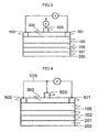
FIG. 3 shows another thermoelectric conversion device including the Heusler alloy film 100 laminated on the substrate having a small thermal conductivity, through the buffer layer 201 and the seed layer 202, a pair of the electrode 501 and the electrode 502, and an electrode 503 on the Heusler alloy film 100 through an insulation film 300. An electromotive force (thermal electromotive force) generated by thermal gradient in the Heusler alloy film 100 is taken out between a pair of the electrodes 501 and 502. The Heusler alloy film 100 has a crystal structure of B2 or L21 in notation of A2BC. In the A2BC notation, elements used as A,B, and C are as follows:
A: a single element or a plurality of elements in the seventh to tenth groups of the fourth to sixth periods in the periodic table, and the crystal structure is formed with the single element or these more than one elements.
B: a single element or a plurality of elements in the fourth to sixth groups of the fourth to sixth periods in the periodic table, and the crystal structure is formed with the single element or these more than one of the elements.
C: a single element or a plurality of elements in the thirteenth to fourteenth groups of the third to sixth periods in the periodic table, and the crystal structure is formed with the single element or this more than one element.
For the buffer layer 201, Ta, Ru, Ti, and Zr are used. For the seed layer 202, a material having a body-centered cubic (bcc) structure such as V, Cr, and W or MgO, MgZnO, etc. is preferably used. Use of such materials for the seed layer 202 enables formation of the Heusler alloy film stably having B2 or L21 structure. In addition, formation of the Heusler alloy film stably having B2 or L21 structure can be provided by heating the substrate at a temperature equal to or higher than 300° C. in producing the Heusler alloy film or by a heat treatment at a temperature equal to or higher than 300° C. after production of the Heusler alloy film. The thermoelectric conversion device shown in FIG. 3 can apply an electric field to the Heusler alloy film 100 through the insulation film 300 by applying a voltage to the insulation film 300 from a power supply E externally installed. This can increase an electric conductivity σ and the Seebeck coefficient S of the Heusler alloy film 100. Hereinafter will be described a principle and operation in a case where Fe2VAl, Fe2NbAl, Fe2TiSi, and Fe2TiSn are adopted for the Heusler alloy film 100. FIGS. 6A to 6D show increase quantities of the performance index Z of these Heusler alloy materials with respect to the voltage Vg applied to the electrodes 503. In each of the charts in FIGS. 6A to 6D, the performance index Z rapidly increases from voltages indicated by arrows. For example, in the case of Fe2VAl, increase in the performance index Z is possible by applying a positive voltage, i.e., 0.5 V or a negative voltage, i.e., −0.3 V, so that increase is expected to be thirty-times increase to the maximum. FIG. 7 shows a table to show optimum application voltages of the four kinds of materials described above. From this table, it is found that in Fe2TiSn, the increase in the performance index Z is possible at a low voltage of −0.1V. Next, with reference to FIG. 8, will be described a principle of increase in the performance index Z by the applied voltage. FIG. 8A shows a typical density of state of the Heusler metal film. The density of state indicates the number of electrons for each energy state. A vertical axis in FIG. 8A represents energy, and the horizontal axis represents the density of states of electrons (DOS). Fermi energy (EF) indicated in FIG. 8A represents an energy of electrons are caused to be finally occupied in a band while electrons are caused to be occupied in bands from a lower energy band. When the voltage Vg is applied to the electrodes 503 to apply an electric field to the Heusler alloy film, the Fermi energy of the Heusler alloy increases by the applied voltage Vg (eV), and the density of state changes to a density of state DOS (Vg). In the example in FIG. 8A, an energy EF indicated with a solid line shifts to an energy EF indicated by broken lines from the state in which the voltage Vg is not applied to the state in which the voltage Vg is applied. The density of state DOS when the voltage Vg is applied increases and an inclination to energy is steep in comparison of the density of state DOS when Vg=0. Here, because the Seebeck index S defining the performance index Z is proportional to an inclination of the energy of the density of state DOS, the electric conductivity σ is proportional to the density of state DOS, an appropriate variation of the voltage Vg provides a state in which increase in both of the Seebeck index S and the electric conductivity σ are allowed. FIGS. 8A and 8C show Vg dependencies of the electric conductivity σ and the Seebeck coefficient Vg of the Heusler structure having the density of state shown in FIG. 8A. As shown in FIGS. 8B and 8C, it becomes possible that the electric conductivity σ increases with respect to the voltage Vg and the Seebeck coefficient S has a local maximum at a certain Vg value.
FIG. 4 shows an example of the thermoelectric conversion device allowing the electromotive force generated by the Heusler alloy film 100 itself to be applied to the electrode 503 through a line 506 in addition to the configuration shown in FIG. 3. This configuration provides a thermoelectric conversion device which does not require external power to be consumed because an external power supply is not used. Because the electromotive force generated by the thermoelectric conversion device itself has a level necessary for the application voltage shown in FIG. 7, it is possible that the performance index Z can be increased by the electromotive force generated by the thermoelectric conversion device itself.
FIG. 9 shows a configuration of a thermoelectric conversion device in which a plurality of single thermoelectric conversion devices shown in FIG. 3 are disposed in an array, and the electrodes 501 and 502 have a shared connection among a plurality of the thermoelectric conversion devices. This configuration can increase the electromotive force which is taken out from a plurality of the thermoelectric conversion devices. In addition, the electrode 503 and the electrode 504 are disposed so as to cross each other above the other part of the thermoelectric conversion device, and voltages applied to the electrodes 503 and the electrode 504 are controlled to select one or more thermoelectric conversion device to which the voltage Vg is applied. For example, the thermoelectric device at a cross point between the electrode 503 supplied with Vg/2 and the electrode 504 supplied with −Vg/2 is not supplied with any voltage, because a total voltage is zero (Vg=0). On the other hand, the thermoelectric device at a cross point between the electrode 503 supplied with Vg/2 and the electrode 504 supplied with Vg/2 is supplied with a total of voltage of Vg (Vg=Vg).
FIG. 10 shows a configuration of a thermoelectric conversion device in which a plurality of single thermoelectric conversion devices shown in FIG. 4 are disposed in an array, and the electrodes 501 and 502 have a shared connection among a plurality of the thermoelectric conversion devices. In this embodiment, the shared connection is a parallel connection of the thermoelectric conversion devices arranged in a line. This configuration can increase the electromotive force which is taken out from a plurality of the thermoelectric conversion devices by the parallel connection similar to the configuration shown in FIG. 9.
FIG. 11 shows a configuration of a thermoelectric conversion device in which a plurality of single thermoelectric conversion devices shown in FIG. 4 are connected in series and may be disposed in an array, and the electrodes 501 and 502 have a shared connection among a plurality of the thermoelectric conversion devices. In this embodiment, the shared connection is a series connection of the thermoelectric conversion devices. Accordingly, the electromotive force (voltage) can be increased, because the electromotive force is taken out from a plurality of the thermoelectric conversion devices.
According to the present invention, the performance index Z can be increased as much as thirty-times or more the conventional performance indexes.

Claims (4)

The invention claimed is:
1. A thermoelectric conversion device comprising:
at least one single thermoelectric conversion device, each at least one single thermoelectric conversion device including:
a Heusler alloy film;
a pair of electrodes on the Heusler alloy film at a predetermined distance therebetween to output an electromotive force generated by a thermal gradient in the Heusler alloy film;
an insulation film on the Heusler alloy film;
a gate electrode on the Heusler alloy film configured to apply an electric field or a voltage to the Heusler alloy film through the insulation film;
a buffer layer, wherein the buffer layer comprises Ta, Ru, Ti or Zr;
a seed layer on the buffer layer, wherein the seed layer comprises V, Cr, W, MgO or MgZnO; and
wherein the Heusler alloy film has a crystal structure of L21 and is disposed on the buffer layer.
2. The thermoelectric conversion device as claimed in claim 1, wherein each Heusler alloy film comprises Fe2TiSn.
3. The thermoelectric conversion device as claimed in claim 1, wherein the at least one single thermoelectric conversion device comprises a plurality of single thermoelectric conversion devices.
4. The thermoelectric conversion device as claimed in claim 3, wherein each of the Heusler alloy films comprise Fe2TiSn.
US14/635,764 2010-12-28 2015-03-02 Thermoelectric conversion device Expired - Fee Related US9559280B2 (en)

Priority Applications (1)

Application Number Priority Date Filing Date Title
US14/635,764 US9559280B2 (en) 2010-12-28 2015-03-02 Thermoelectric conversion device

Applications Claiming Priority (4)

Application Number Priority Date Filing Date Title
JP2010291527A JP5723591B2 (en) 2010-12-28 2010-12-28 Thermoelectric conversion materials and electric field applied thermoelectric conversion elements
JP2010-291527 2010-12-28
US13/338,740 US20120160288A1 (en) 2010-12-28 2011-12-28 Thermoelectric conversion device
US14/635,764 US9559280B2 (en) 2010-12-28 2015-03-02 Thermoelectric conversion device

Related Parent Applications (1)

Application Number Title Priority Date Filing Date
US13/338,740 Division US20120160288A1 (en) 2010-12-28 2011-12-28 Thermoelectric conversion device

Publications (2)

Publication Number Publication Date
US20150280095A1 US20150280095A1 (en) 2015-10-01
US9559280B2 true US9559280B2 (en) 2017-01-31

Family

ID=46315220

Family Applications (2)

Application Number Title Priority Date Filing Date
US13/338,740 Abandoned US20120160288A1 (en) 2010-12-28 2011-12-28 Thermoelectric conversion device
US14/635,764 Expired - Fee Related US9559280B2 (en) 2010-12-28 2015-03-02 Thermoelectric conversion device

Family Applications Before (1)

Application Number Title Priority Date Filing Date
US13/338,740 Abandoned US20120160288A1 (en) 2010-12-28 2011-12-28 Thermoelectric conversion device

Country Status (2)

Country Link
US (2) US20120160288A1 (en)
JP (1) JP5723591B2 (en)

Families Citing this family (4)

* Cited by examiner, † Cited by third party
Publication number Priority date Publication date Assignee Title
JP5775163B2 (en) * 2011-09-05 2015-09-09 株式会社日立製作所 Thermoelectric conversion element and thermoelectric conversion module using the same
DE102013004173B3 (en) * 2013-03-11 2014-03-06 Fraunhofer-Gesellschaft zur Förderung der angewandten Forschung e.V. Thermogenerator for generating electrical energy from thermal energy and method for its production
JP6617840B2 (en) * 2017-01-20 2019-12-11 日立金属株式会社 P-type thermoelectric conversion material, thermoelectric conversion module, and method for producing p-type thermoelectric conversion material
JP6859805B2 (en) * 2017-03-30 2021-04-14 Tdk株式会社 Laminated body, thermoelectric conversion element

Citations (12)

* Cited by examiner, † Cited by third party
Publication number Priority date Publication date Assignee Title
JPH0669549A (en) 1992-08-14 1994-03-11 Matsushita Electric Ind Co Ltd Thermoelectric device
JP2000058931A (en) 1998-08-14 2000-02-25 Honda Motor Co Ltd Thermoelectric conversion element and thermoelectric conversion module
WO2003019681A1 (en) 2001-08-23 2003-03-06 Nagoya Industrial Science Research Institute Thermoelectric transducing material, method for preparation thereof and thermoelectric transducer
JP2003197985A (en) 2001-12-28 2003-07-11 Toshiba Corp Thermoelectric conversion material and thermoelectric conversion element using the same
JP2004119648A (en) 2002-09-26 2004-04-15 Toshiba Corp P-type thermoelectric conversion material and thermoelectric conversion element using the same
JP2005116680A (en) 2003-10-06 2005-04-28 Toshiba Corp Thermoelectric conversion material and thermoelectric conversion element using the same
US20070034245A1 (en) 2004-04-21 2007-02-15 Showa Denko K.K. Process for producing thermoelectric semiconductor alloy, thermoelectric conversion module, thermoelectric power generating device, rare earth alloy, producing process thereof, thermoelectric conversion material, and thermoelectric conversion system using filled skutterudite based alloy
US20070125414A1 (en) 2005-12-01 2007-06-07 Raytheon Company Thermoelectric bias voltage generator
JP2008192652A (en) 2007-01-31 2008-08-21 National Institute Of Advanced Industrial & Technology Composite thermoelectric conversion material
JP2008218640A (en) 2007-03-02 2008-09-18 Tohoku Univ Tunnel magnetoresistive element
JP2009117430A (en) 2007-11-02 2009-05-28 Toyota Central R&D Labs Inc Thermoelectric element
JP2010229477A (en) 2009-03-26 2010-10-14 Tohoku Univ Heusler alloy material, magnetoresistive element and magnetic device

Patent Citations (12)

* Cited by examiner, † Cited by third party
Publication number Priority date Publication date Assignee Title
JPH0669549A (en) 1992-08-14 1994-03-11 Matsushita Electric Ind Co Ltd Thermoelectric device
JP2000058931A (en) 1998-08-14 2000-02-25 Honda Motor Co Ltd Thermoelectric conversion element and thermoelectric conversion module
WO2003019681A1 (en) 2001-08-23 2003-03-06 Nagoya Industrial Science Research Institute Thermoelectric transducing material, method for preparation thereof and thermoelectric transducer
JP2003197985A (en) 2001-12-28 2003-07-11 Toshiba Corp Thermoelectric conversion material and thermoelectric conversion element using the same
JP2004119648A (en) 2002-09-26 2004-04-15 Toshiba Corp P-type thermoelectric conversion material and thermoelectric conversion element using the same
JP2005116680A (en) 2003-10-06 2005-04-28 Toshiba Corp Thermoelectric conversion material and thermoelectric conversion element using the same
US20070034245A1 (en) 2004-04-21 2007-02-15 Showa Denko K.K. Process for producing thermoelectric semiconductor alloy, thermoelectric conversion module, thermoelectric power generating device, rare earth alloy, producing process thereof, thermoelectric conversion material, and thermoelectric conversion system using filled skutterudite based alloy
US20070125414A1 (en) 2005-12-01 2007-06-07 Raytheon Company Thermoelectric bias voltage generator
JP2008192652A (en) 2007-01-31 2008-08-21 National Institute Of Advanced Industrial & Technology Composite thermoelectric conversion material
JP2008218640A (en) 2007-03-02 2008-09-18 Tohoku Univ Tunnel magnetoresistive element
JP2009117430A (en) 2007-11-02 2009-05-28 Toyota Central R&D Labs Inc Thermoelectric element
JP2010229477A (en) 2009-03-26 2010-10-14 Tohoku Univ Heusler alloy material, magnetoresistive element and magnetic device

Non-Patent Citations (6)

* Cited by examiner, † Cited by third party
Title
English machine translation of JP 2009-117430A.
Geiersbach et al., "Structural, magnetic and magnetotransport properties of thin films of the Heusler alloys Cu2MnAl, Co2MnSi, Co2MnGe and Co2MnSn." Journal of Magnetism and Magnetic materials 240 (2002) 546-549.
Lue et al., "Thermal and transport properties of the Heusler-type compounds Fe2-xTil+xSn." Journal of Applied Physics 96, 2681 (2004).
Nakabayashi, M. et al., "Semiconductor Behavior of Fe2TiSn Heusler Alloy," Summary of Lecture by Japan Institute of Metals, Japan 2002, 130th.
Office Action in Japanese Patent Appln. 2010-291527, dispatched Aug. 26, 2014 (2 pgs., in Japanese); [2 pgs., English language translation].
Office Action in Japanese Patent Appln. 2010-291527, dispatched Feb. 4, 2014 (5 pgs., in Japanese); [3 pgs., English language translation].

Also Published As

Publication number Publication date
US20150280095A1 (en) 2015-10-01
JP2012138539A (en) 2012-07-19
JP5723591B2 (en) 2015-05-27
US20120160288A1 (en) 2012-06-28

Similar Documents

Publication Publication Date Title
He et al. Advances in thermoelectric materials research: Looking back and moving forward
US8455751B2 (en) Thermoelectric devices and applications for the same
US6828579B2 (en) Thermoelectric device with Si/SiC superlattice N-legs
Zhang et al. Mechanical properties and thermal stability of the high-thermoelectric-performance Cu2Se compound
US9559280B2 (en) Thermoelectric conversion device
CN1836340A (en) Low power thermoelectric generator
US20150155464A1 (en) Thermoelectric Structures and Devices Based on Topological Insulators
US20140345663A1 (en) Thermoelectric device and thermoelectric module using the same
KR101779497B1 (en) Thermoelectric module comprising thermoelectric element doped with nanoparticles and manufacturing method of the same
JP5775163B2 (en) Thermoelectric conversion element and thermoelectric conversion module using the same
Mandrus et al. Unusual transport and large diamagnetism in the intermetallic semiconductor RuAl 2
Zou et al. Band engineering via biaxial strain for enhanced thermoelectric performance in stannite-type Cu 2 ZnSnSe 4
KR20170010647A (en) Thermo electric element and cooling apparatus comprising the same
Kim et al. Realization of high‐performance screen‐printed flexible thermoelectric generator by improving contact characteristics
Botana et al. All-3 d electron-hole bilayers in CrN/MgO (111) multilayers for thermoelectric applications
US20140373891A1 (en) Thermoelectric structure, and thermoelectric device and thermoelectric apparatus including the same
Budak et al. Superlattice multinanolayered thin films of SiO2/SiO2+ Ge for thermoelectric device applications
Goldsmid Bismuth--The Thermoelectric Material of the Future?
US10580957B2 (en) Thermoelectric material structure
Budak et al. MeV Si ions bombardments effects on thermoelectric properties of SiO2/SiO2+ Ge nanolayers
Li et al. Grain boundaries softening thermoelectric oxide BiCuSeO
US20130180560A1 (en) Nanoscale, ultra-thin films for excellent thermoelectric figure of merit
US20130160808A1 (en) Thermoelectric generating apparatus and module
FU et al. Effect of Microstructure in Understanding the Electronic Properties of Complex Materials
JP6439509B2 (en) Thermoelectric conversion element, thermoelectric conversion module, and method of manufacturing thermoelectric conversion element

Legal Events

Date Code Title Description
STCF Information on status: patent grant

Free format text: PATENTED CASE

MAFP Maintenance fee payment

Free format text: PAYMENT OF MAINTENANCE FEE, 4TH YEAR, LARGE ENTITY (ORIGINAL EVENT CODE: M1551); ENTITY STATUS OF PATENT OWNER: LARGE ENTITY

Year of fee payment: 4

FEPP Fee payment procedure

Free format text: MAINTENANCE FEE REMINDER MAILED (ORIGINAL EVENT CODE: REM.); ENTITY STATUS OF PATENT OWNER: LARGE ENTITY

LAPS Lapse for failure to pay maintenance fees

Free format text: PATENT EXPIRED FOR FAILURE TO PAY MAINTENANCE FEES (ORIGINAL EVENT CODE: EXP.); ENTITY STATUS OF PATENT OWNER: LARGE ENTITY

STCH Information on status: patent discontinuation

Free format text: PATENT EXPIRED DUE TO NONPAYMENT OF MAINTENANCE FEES UNDER 37 CFR 1.362

FP Lapsed due to failure to pay maintenance fee

Effective date: 20250131