US9553104B2 - Semiconductor device and method of fabricating the same - Google Patents
Semiconductor device and method of fabricating the same Download PDFInfo
- Publication number
- US9553104B2 US9553104B2 US14/733,508 US201514733508A US9553104B2 US 9553104 B2 US9553104 B2 US 9553104B2 US 201514733508 A US201514733508 A US 201514733508A US 9553104 B2 US9553104 B2 US 9553104B2
- Authority
- US
- United States
- Prior art keywords
- layer
- height
- fin structures
- dielectric
- comb
- Prior art date
- Legal status (The legal status is an assumption and is not a legal conclusion. Google has not performed a legal analysis and makes no representation as to the accuracy of the status listed.)
- Active
Links
- 239000004065 semiconductor Substances 0.000 title claims abstract description 43
- 238000004519 manufacturing process Methods 0.000 title description 3
- 239000004020 conductor Substances 0.000 claims abstract description 40
- 239000000758 substrate Substances 0.000 claims abstract description 38
- 238000003860 storage Methods 0.000 claims description 26
- 238000000034 method Methods 0.000 abstract description 51
- 239000010410 layer Substances 0.000 description 157
- 239000000463 material Substances 0.000 description 32
- 238000005530 etching Methods 0.000 description 23
- 238000000059 patterning Methods 0.000 description 21
- 239000003989 dielectric material Substances 0.000 description 8
- 229910052710 silicon Inorganic materials 0.000 description 8
- XUIMIQQOPSSXEZ-UHFFFAOYSA-N Silicon Chemical compound [Si] XUIMIQQOPSSXEZ-UHFFFAOYSA-N 0.000 description 7
- 238000005229 chemical vapour deposition Methods 0.000 description 7
- 239000010703 silicon Substances 0.000 description 7
- 229920002120 photoresistant polymer Polymers 0.000 description 6
- 150000004767 nitrides Chemical class 0.000 description 5
- 239000006117 anti-reflective coating Substances 0.000 description 4
- 239000011248 coating agent Substances 0.000 description 4
- 238000000576 coating method Methods 0.000 description 4
- 238000001312 dry etching Methods 0.000 description 4
- 229910021420 polycrystalline silicon Inorganic materials 0.000 description 4
- 229920005591 polysilicon Polymers 0.000 description 4
- 239000002356 single layer Substances 0.000 description 4
- 229910052581 Si3N4 Inorganic materials 0.000 description 3
- 230000003647 oxidation Effects 0.000 description 3
- 238000007254 oxidation reaction Methods 0.000 description 3
- HQVNEWCFYHHQES-UHFFFAOYSA-N silicon nitride Chemical compound N12[Si]34N5[Si]62N3[Si]51N64 HQVNEWCFYHHQES-UHFFFAOYSA-N 0.000 description 3
- QNRATNLHPGXHMA-XZHTYLCXSA-N (r)-(6-ethoxyquinolin-4-yl)-[(2s,4s,5r)-5-ethyl-1-azabicyclo[2.2.2]octan-2-yl]methanol;hydrochloride Chemical compound Cl.C([C@H]([C@H](C1)CC)C2)CN1[C@@H]2[C@H](O)C1=CC=NC2=CC=C(OCC)C=C21 QNRATNLHPGXHMA-XZHTYLCXSA-N 0.000 description 2
- VYPSYNLAJGMNEJ-UHFFFAOYSA-N Silicium dioxide Chemical compound O=[Si]=O VYPSYNLAJGMNEJ-UHFFFAOYSA-N 0.000 description 2
- 229910000577 Silicon-germanium Inorganic materials 0.000 description 2
- 229910003481 amorphous carbon Inorganic materials 0.000 description 2
- 230000000694 effects Effects 0.000 description 2
- 239000012212 insulator Substances 0.000 description 2
- 238000001459 lithography Methods 0.000 description 2
- 238000012986 modification Methods 0.000 description 2
- 230000004048 modification Effects 0.000 description 2
- 238000001020 plasma etching Methods 0.000 description 2
- 229910052814 silicon oxide Inorganic materials 0.000 description 2
- 238000000992 sputter etching Methods 0.000 description 2
- 229910005540 GaP Inorganic materials 0.000 description 1
- 229910001218 Gallium arsenide Inorganic materials 0.000 description 1
- 229910000673 Indium arsenide Inorganic materials 0.000 description 1
- 229910003811 SiGeC Inorganic materials 0.000 description 1
- LEVVHYCKPQWKOP-UHFFFAOYSA-N [Si].[Ge] Chemical compound [Si].[Ge] LEVVHYCKPQWKOP-UHFFFAOYSA-N 0.000 description 1
- 230000015572 biosynthetic process Effects 0.000 description 1
- 239000002131 composite material Substances 0.000 description 1
- 230000003247 decreasing effect Effects 0.000 description 1
- RWRIWBAIICGTTQ-UHFFFAOYSA-N difluoromethane Chemical compound FCF RWRIWBAIICGTTQ-UHFFFAOYSA-N 0.000 description 1
- NBVXSUQYWXRMNV-UHFFFAOYSA-N fluoromethane Chemical compound FC NBVXSUQYWXRMNV-UHFFFAOYSA-N 0.000 description 1
- 229910052732 germanium Inorganic materials 0.000 description 1
- RPQDHPTXJYYUPQ-UHFFFAOYSA-N indium arsenide Chemical compound [In]#[As] RPQDHPTXJYYUPQ-UHFFFAOYSA-N 0.000 description 1
- 230000010354 integration Effects 0.000 description 1
- 229910003465 moissanite Inorganic materials 0.000 description 1
- 229920001558 organosilicon polymer Polymers 0.000 description 1
- 229920000548 poly(silane) polymer Polymers 0.000 description 1
- 230000000717 retained effect Effects 0.000 description 1
- 229910010271 silicon carbide Inorganic materials 0.000 description 1
- 238000004528 spin coating Methods 0.000 description 1
- SFZCNBIFKDRMGX-UHFFFAOYSA-N sulfur hexafluoride Chemical compound FS(F)(F)(F)(F)F SFZCNBIFKDRMGX-UHFFFAOYSA-N 0.000 description 1
Images


Classifications
-
- H01L27/11582—
-
- H—ELECTRICITY
- H01—ELECTRIC ELEMENTS
- H01L—SEMICONDUCTOR DEVICES NOT COVERED BY CLASS H10
- H01L21/00—Processes or apparatus adapted for the manufacture or treatment of semiconductor or solid state devices or of parts thereof
- H01L21/02—Manufacture or treatment of semiconductor devices or of parts thereof
- H01L21/027—Making masks on semiconductor bodies for further photolithographic processing not provided for in group H01L21/18 or H01L21/34
- H01L21/033—Making masks on semiconductor bodies for further photolithographic processing not provided for in group H01L21/18 or H01L21/34 comprising inorganic layers
- H01L21/0332—Making masks on semiconductor bodies for further photolithographic processing not provided for in group H01L21/18 or H01L21/34 comprising inorganic layers characterised by their composition, e.g. multilayer masks, materials
-
- H01L21/28282—
-
- H—ELECTRICITY
- H01—ELECTRIC ELEMENTS
- H01L—SEMICONDUCTOR DEVICES NOT COVERED BY CLASS H10
- H01L21/00—Processes or apparatus adapted for the manufacture or treatment of semiconductor or solid state devices or of parts thereof
- H01L21/02—Manufacture or treatment of semiconductor devices or of parts thereof
- H01L21/04—Manufacture or treatment of semiconductor devices or of parts thereof the devices having at least one potential-jump barrier or surface barrier, e.g. PN junction, depletion layer or carrier concentration layer
- H01L21/18—Manufacture or treatment of semiconductor devices or of parts thereof the devices having at least one potential-jump barrier or surface barrier, e.g. PN junction, depletion layer or carrier concentration layer the devices having semiconductor bodies comprising elements of Group IV of the Periodic System or AIIIBV compounds with or without impurities, e.g. doping materials
- H01L21/30—Treatment of semiconductor bodies using processes or apparatus not provided for in groups H01L21/20 - H01L21/26
- H01L21/31—Treatment of semiconductor bodies using processes or apparatus not provided for in groups H01L21/20 - H01L21/26 to form insulating layers thereon, e.g. for masking or by using photolithographic techniques; After treatment of these layers; Selection of materials for these layers
- H01L21/3205—Deposition of non-insulating-, e.g. conductive- or resistive-, layers on insulating layers; After-treatment of these layers
- H01L21/321—After treatment
- H01L21/32115—Planarisation
-
- H—ELECTRICITY
- H01—ELECTRIC ELEMENTS
- H01L—SEMICONDUCTOR DEVICES NOT COVERED BY CLASS H10
- H01L21/00—Processes or apparatus adapted for the manufacture or treatment of semiconductor or solid state devices or of parts thereof
- H01L21/02—Manufacture or treatment of semiconductor devices or of parts thereof
- H01L21/04—Manufacture or treatment of semiconductor devices or of parts thereof the devices having at least one potential-jump barrier or surface barrier, e.g. PN junction, depletion layer or carrier concentration layer
- H01L21/18—Manufacture or treatment of semiconductor devices or of parts thereof the devices having at least one potential-jump barrier or surface barrier, e.g. PN junction, depletion layer or carrier concentration layer the devices having semiconductor bodies comprising elements of Group IV of the Periodic System or AIIIBV compounds with or without impurities, e.g. doping materials
- H01L21/30—Treatment of semiconductor bodies using processes or apparatus not provided for in groups H01L21/20 - H01L21/26
- H01L21/31—Treatment of semiconductor bodies using processes or apparatus not provided for in groups H01L21/20 - H01L21/26 to form insulating layers thereon, e.g. for masking or by using photolithographic techniques; After treatment of these layers; Selection of materials for these layers
- H01L21/3205—Deposition of non-insulating-, e.g. conductive- or resistive-, layers on insulating layers; After-treatment of these layers
- H01L21/321—After treatment
- H01L21/3213—Physical or chemical etching of the layers, e.g. to produce a patterned layer from a pre-deposited extensive layer
- H01L21/32133—Physical or chemical etching of the layers, e.g. to produce a patterned layer from a pre-deposited extensive layer by chemical means only
-
- H—ELECTRICITY
- H01—ELECTRIC ELEMENTS
- H01L—SEMICONDUCTOR DEVICES NOT COVERED BY CLASS H10
- H01L21/00—Processes or apparatus adapted for the manufacture or treatment of semiconductor or solid state devices or of parts thereof
- H01L21/02—Manufacture or treatment of semiconductor devices or of parts thereof
- H01L21/04—Manufacture or treatment of semiconductor devices or of parts thereof the devices having at least one potential-jump barrier or surface barrier, e.g. PN junction, depletion layer or carrier concentration layer
- H01L21/18—Manufacture or treatment of semiconductor devices or of parts thereof the devices having at least one potential-jump barrier or surface barrier, e.g. PN junction, depletion layer or carrier concentration layer the devices having semiconductor bodies comprising elements of Group IV of the Periodic System or AIIIBV compounds with or without impurities, e.g. doping materials
- H01L21/30—Treatment of semiconductor bodies using processes or apparatus not provided for in groups H01L21/20 - H01L21/26
- H01L21/31—Treatment of semiconductor bodies using processes or apparatus not provided for in groups H01L21/20 - H01L21/26 to form insulating layers thereon, e.g. for masking or by using photolithographic techniques; After treatment of these layers; Selection of materials for these layers
- H01L21/3205—Deposition of non-insulating-, e.g. conductive- or resistive-, layers on insulating layers; After-treatment of these layers
- H01L21/321—After treatment
- H01L21/3213—Physical or chemical etching of the layers, e.g. to produce a patterned layer from a pre-deposited extensive layer
- H01L21/32139—Physical or chemical etching of the layers, e.g. to produce a patterned layer from a pre-deposited extensive layer using masks
-
- H—ELECTRICITY
- H01—ELECTRIC ELEMENTS
- H01L—SEMICONDUCTOR DEVICES NOT COVERED BY CLASS H10
- H01L29/00—Semiconductor devices adapted for rectifying, amplifying, oscillating or switching, or capacitors or resistors with at least one potential-jump barrier or surface barrier, e.g. PN junction depletion layer or carrier concentration layer; Details of semiconductor bodies or of electrodes thereof ; Multistep manufacturing processes therefor
- H01L29/40—Electrodes ; Multistep manufacturing processes therefor
- H01L29/401—Multistep manufacturing processes
- H01L29/4011—Multistep manufacturing processes for data storage electrodes
- H01L29/40117—Multistep manufacturing processes for data storage electrodes the electrodes comprising a charge-trapping insulator
-
- H—ELECTRICITY
- H10—SEMICONDUCTOR DEVICES; ELECTRIC SOLID-STATE DEVICES NOT OTHERWISE PROVIDED FOR
- H10B—ELECTRONIC MEMORY DEVICES
- H10B43/00—EEPROM devices comprising charge-trapping gate insulators
- H10B43/20—EEPROM devices comprising charge-trapping gate insulators characterised by three-dimensional arrangements, e.g. with cells on different height levels
- H10B43/23—EEPROM devices comprising charge-trapping gate insulators characterised by three-dimensional arrangements, e.g. with cells on different height levels with source and drain on different levels, e.g. with sloping channels
- H10B43/27—EEPROM devices comprising charge-trapping gate insulators characterised by three-dimensional arrangements, e.g. with cells on different height levels with source and drain on different levels, e.g. with sloping channels the channels comprising vertical portions, e.g. U-shaped channels
Definitions
- the invention relates to a semiconductor device and a method of fabricating the same.
- semiconductor devices With the integration of semiconductor devices, in order to achieve high density and high performance, fabrication of semiconductor devices has evolved into stacking upward in the vertical direction, such that the wafer area can be used more efficiently. Therefore, semiconductor structures or openings having a high aspect ratio are common in small-sized devices.
- the patterning process is usually carried out with very high etching selectivity in order to form trenches having a high aspect ratio.
- very high etching selectivity the problem of residual material layer on the sidewall of the trench may occur. If there is residual material layer on the sidewall of the trench and the residual material layer is conductive, improper conduction may occur between the semiconductor devices and impair the electrical performance of the devices.
- how to pattern the material layer (conductive layer) in the semiconductor structure with the trench having a high aspect ratio without leaving residual material layer on the sidewall of the trench is an issue that needs to be addressed.
- the invention provides a fabricating method of a semiconductor device for patterning a material layer (conductive layer) in a semiconductor structure with a trench having a high aspect ratio decreasing or without leaving a residue of the material layer on sidewalls of the trench.
- the invention provides a fabricating method of a semiconductor device.
- the fabricating method of the semiconductor device includes the following.
- a plurality of fin structures are formed on a substrate, and the adjacent fin structures have an opening therebetween.
- a conductive material layer is formed to cover the fin structures and fill the opening.
- the conductive material layer and the fin structures are patterned to form a mesh structure.
- the mesh structure includes a plurality of first strips extending in a first direction and a plurality of second strips extending in a second direction. The first strips and the second strips intersect one another, and the mesh structure has a plurality of holes.
- the first strips are located on the substrate at positions corresponding to the fin structures.
- the second strips are located on the substrate, and the conductive material layer in the second strips spans the fin structures.
- the hole is respectively located in the opening and surrounded by the first strips and the second strips, and the holes extend to positions closer to the substrate than bottoms of the fin structures.
- the step of patterning the conductive material layer and the fin structures includes performing a non-selective etching process.
- an etching selectivity of the conductive material layer and the fin structures is controlled to be 0.7 to 1.3 for performing the non-selective etching process.
- the fabricating method further includes performing a planarization process on the conductive material layer before patterning the conductive material layer and the fin structures.
- the fin structures and the conductive material layer are patterned such that a height of a sidewall of each hole in the mesh structure is greater than a height of the first strip.
- the height of the sidewall of each hole in the mesh structure exceeds the height of the first strip by 30% or more of the height of the first strip.
- the step of forming the fin structures includes the following.
- a stack layer is formed on the substrate.
- the stack layer includes at least one conductive layer and at least one dielectric layer that are stacked alternately.
- a charge storage layer is formed to cover the substrate at a bottom of the opening and a surface of the stack layer.
- the fabricating method further includes the following.
- a plurality of dielectric pillars are formed to at least fill the holes.
- the conductive material layer in the first strips and the dielectric pillars are patterned such that the patterned conductive material layer forms a plurality of comb structures.
- Each comb structure includes a plurality of comb portions and a connection portion. The comb portions are respectively inserted into the opening between the adjacent fin structures and are in contact with sidewalls of the adjacent fin structures.
- the connection portion extends in the second direction and is located on the fin structures to connect the comb portions.
- the conductive material layer in the first strips and the dielectric pillars are patterned such that a length of the connection portion in the first direction is smaller than a length of each dielectric pillar in the first direction.
- a portion of the fin structures and the dielectric pillars between the connection portion in the adjacent comb structures is removed by performing an over etching process.
- the step of forming the dielectric pillars and patterning the conductive material layer in the first strips and the dielectric pillars includes the following.
- a dielectric material layer is formed to cover the mesh structure and fill the holes.
- the dielectric material layer and the conductive material layer in the first strips are patterned to form the comb structures, a plurality of cap layers, and the dielectric pillars.
- Each comb structure includes the comb portions and the connection portion.
- Each cap layer is located on the connection portion and extends in the second direction.
- the invention further provides a semiconductor device.
- the semiconductor device includes a substrate, a plurality of fin structures, a plurality of comb structures, and a plurality of dielectric pillars.
- the fin structures are located on the substrate and extend in a first direction.
- the adjacent fin structures have an opening therebetween.
- the comb structures include a conductive material, and each of the comb structures includes a plurality of comb portions and a connection portion.
- the comb portions are respectively inserted into the opening between the adjacent fin structures and are in contact with sidewalls of the adjacent fin structures.
- the connection portion extends in the second direction and is located on the fin structures to connect the comb portions.
- the dielectric pillars are respectively inserted into the opening between the adjacent fin structures and are in contact with the sidewalls of the adjacent fin structures and the comb portions.
- the dielectric pillars extend to positions closer to the substrate than bottoms of the fin structures.
- the fin structures respectively include a stack layer and a charge storage layer.
- the stack layer includes at least one conductive layer and at least one dielectric layer stacked alternately.
- the charge storage layer covers the substrate at a bottom of the opening and a surface of the stack layer.
- a first angle of the fin structures is smaller than a second angle of the comb portions.
- the first angle is an angle between the sidewall of the fin structure and the surface of the substrate.
- the second angle is an angle between a sidewall of the comb portion and the surface of the substrate.
- the dielectric pillars have different heights.
- each dielectric pillar is greater than a height of each fin structure.
- the height of each dielectric pillar exceeds the height of each fin structure by 30% or more of the height of the fin structure.
- a length of the connection portion in the first direction is smaller than a length of each dielectric pillar in the first direction.
- a first height of a portion of each fin structure is smaller than a second height of another portion of the fin structure.
- the first height is a height of each fin structure between the adjacent comb structures.
- the second height is a height of each fin structure under the comb structure.
- the semiconductor device further includes a plurality of cap layers.
- the cap layers are located on the connection portion and extend in the second direction.
- the fin structures and the material layer (conductive layer) are patterned simultaneously to form the mesh structure.
- the material layer (conductive layer) in the semiconductor structure with the trench having a high aspect ratio is patterned without leaving a residue of the material layer on the sidewall of the trench. This method effectively prevents improper conduction between the semiconductor devices and thus improves the electrical performance of the devices.
- FIG. 1A to FIG. 1F are schematic perspective views showing a fabricating method of a semiconductor device according to an embodiment of the invention.
- FIG. 2A to FIG. 2F are schematic cross-sectional views, taken along the line A-A′ of FIG. 1A to FIG. 1F , showing the fabricating method of the semiconductor device.
- FIG. 3A to FIG. 3F are schematic cross-sectional views, taken along the line B-B′ of FIG. 1A to FIG. 1F , showing the fabricating method of the semiconductor device.
- FIG. 4A to FIG. 4F are schematic cross-sectional views, taken along the line C-C′ of FIG. 1A to FIG. 1F , showing the fabricating method of the semiconductor device.
- the substrate 10 may include a semiconductor material, an insulator material, a conductive material, or any combination of the foregoing materials.
- the material of the substrate 10 is a material composed of at least one selected from a group consisting of Si, Ge, SiGe, GaP, GaAs, SiC, SiGeC, InAs, and InP, or any physical structure suitable for a fabricating process of the invention, for example.
- the substrate 10 includes a single-layer structure or a multi-layer structure.
- a silicon on insulator (SOI) substrate may be used as the substrate 10 .
- the substrate 10 is silicon or silicon germanium, for example.
- a dielectric layer 12 is then formed on the substrate 10 .
- the dielectric layer 12 includes an oxide, a nitride, an oxy-nitride, or a low dielectric constant material having a dielectric constant smaller than 4.
- the dielectric layer 12 is a bottom oxide layer (BOX), for example.
- a thickness of the dielectric layer 12 is in a range of 1000 ⁇ to 5000 ⁇ , for example.
- a method of forming the dielectric layer 12 includes performing thermal oxidation or chemical vapor deposition, for example.
- a stack layer 16 is formed on the dielectric layer 12 .
- the stack layer 16 includes a plurality of conductive layers 16 a and a plurality of dielectric layers 16 b that are stacked alternately.
- a material of the conductive layer 16 a includes an undoped semiconductor or a doped semiconductor, such as polysilicon or doped polysilicon.
- a thickness of each conductive layer 16 a is in a range of 1001 to 500 ⁇ , for example.
- a thickness of each dielectric layer 16 b is in a range of 200 ⁇ to 600 ⁇ , for example.
- the dielectric layer 16 b and the dielectric layer 12 may be formed of the same or different materials.
- the material of the dielectric layer 16 b may include an oxide, a nitride, an oxynitride, or a low dielectric constant material having a dielectric constant smaller than 4.
- a method of forming the conductive layer 16 a and the dielectric layer 16 b includes performing thermal oxidation or chemical vapor deposition, for example.
- a charge storage layer 18 is forming to cover a surface of the stack layer 16 and a surface of the dielectric layer 12 , so as to form a plurality of fin structures 14 .
- a material of the charge storage layer 18 includes an oxide, a nitride, or a combination of the foregoing.
- the material of the charge storage layer 18 includes a silicon nitride, a silicon oxide, or a combination of the foregoing.
- the charge storage layer 18 may be a single layer or include multiple layers. In an embodiment, the charge storage layer 18 is a single-layer silicon nitride layer, for example.
- the charge storage layer 18 is a composite layer of oxide/nitride/oxide (ONO), for example.
- a thickness of the charge storage layer 18 is in a range of 100 ⁇ to 300 ⁇ , for example.
- a method of forming the charge storage layer 18 includes performing chemical vapor deposition or thermal oxidation, for example.
- the adjacent fin structures 14 have an opening T therebetween.
- the opening T may be fainted with any length, width, or shape.
- a cross section of the opening T may be in any shape, such as a V shape, a U shape, a rhombic shape, or a combination of the foregoing, for example.
- the invention is not limited thereto.
- each fin structure 14 may selectively include a first hard mask layer 20 .
- the first hard mask layer 20 is disposed between the stack layer 16 and the charge storage layer 18 , for example. Nevertheless, the invention is not limited thereto.
- the first hard mask layer 20 may be a single layer or include multiple layers.
- a material of the first hard mask layer 20 includes a silicon oxide, a silicon nitride, or other materials having a high Young's modulus, for example.
- a thickness of the first hard mask layer 20 is in a range of 100 ⁇ to 1000 ⁇ , for example.
- a method of forming the first hard mask layer 20 includes performing chemical vapor deposition, for example.
- a conductive material layer 22 is disposed to cover the surface of the charge storage layer 18 of the fin structure 14 and the surface of the dielectric layer 12 and fill the opening T.
- the conductive material layer 22 includes an undoped semiconductor or a doped semiconductor, such as polysilicon or doped polysilicon.
- a thickness of the conductive material layer 22 on a top of the fin structure 14 is in a range of 500 ⁇ to 1500 ⁇ , for example.
- a method of forming the conductive material layer 22 includes performing chemical vapor deposition, for example.
- a mask structure 24 is formed on the conductive material layer 22 .
- the mask structure 24 includes a first advanced patterning film (APF) 24 a , a dielectric anti-reflective coating film (DARC) 24 b , a second advanced patterning film 24 c , a silicon-containing hard-mask bottom anti-reflection coating (SHB) 24 d , and a patterned photoresist layer 24 e in sequence.
- a material of the first advanced patterning film 24 a is amorphous carbon, for example.
- a material of the dielectric anti-reflective coating film 24 b is silicon oxynitride, for example.
- a material of the second advanced patterning film 24 c is amorphous carbon, for example.
- a material of the silicon-containing hard-mask bottom anti-reflection coating 24 d is an organosilicon polymer, polysilane, or a combination of the foregoing, for example.
- a material of the patterned photoresist layer 24 e is a positive photoresist, a negative photoresist, or a combination of the foregoing, for example.
- a thickness of the first advanced patterning film 24 a is in a range of 4000 ⁇ to 15000 ⁇ , for example.
- a thickness of the dielectric anti-reflective coating film 24 b is in a range of 300 ⁇ to 2000 ⁇ , for example.
- a thickness of the second advanced patterning film 24 c is in a range of 500 ⁇ to 4000 ⁇ , for example.
- a thickness of the silicon-containing hard-mask bottom anti-reflection coating 24 d is in a range of 200 ⁇ to 1000 ⁇ , for example.
- a thickness of the patterned photoresist layer 24 e is in a range of 200 ⁇ to 3000 ⁇ , for example.
- a method of forming the first advanced patterning film 24 a , the dielectric anti-reflective coating film 24 b , the second advanced patterning film 24 c , and the silicon-containing hard-mask bottom anti-reflection coating 24 d includes performing chemical vapor deposition, for example.
- a method of forming the patterned photoresist layer 24 e includes performing spin coating in combination with a lithography process, for example.
- a planarization process may be performed on the conductive material layer 22 to facilitate the subsequent patterning process.
- the conductive material layer 22 is patterned and a portion of the charge storage layer 18 and a portion of the dielectric layer 12 are removed by performing a non-selective etching process with the mask structure 24 as a mask, so as to form a mesh structure 26 .
- the non-selective etching process means etching the conductive material layer 22 , the charge storage layer 18 , and the dielectric layer 12 at substantially the same etching rate.
- an etching selectivity of the conductive material layer 22 to the charge storage layer 18 and an etching selectivity of the conductive material layer 22 to the dielectric layer 12 are respectively in a range of 0.7 to 1.3, for example. It should be noted that the aforementioned range of the etching selectivity is given as an example, and the invention is not limited thereto. The etching selectivity may be adjusted as required as long as the conductive material layer 22 on the sidewall of the opening for forming an isolating structure can be completely removed.
- the non-selective etching process is a dry etching process, for example.
- the dry etching process may be sputter etching, reactive ion etching, etc.
- a gas used in the non-selective etching process is NF 3 , HBr, CH 4 , N 2 , He, Ar, SF 6 , CH 2 F 2 , and CH 3 F, for example.
- the mesh structure 26 includes a plurality of first strips 26 a and a plurality of second strips 26 b that intersect each other.
- the first strips 26 a extend in a first direction D 1 and are located at positions corresponding to the fin structures 14 . That is, each first strip 26 a includes the fin structure 14 and a first strip conductive layer 25 a on the fin structure 14 .
- the second strips 26 b extend in a second direction D 2 and are located on the substrate 10 .
- a second strip conductive layer 25 b of the second strip 26 b spans the fin structures 14 .
- each second strip 26 b includes a portion of the fin structure 14 and the second strip conductive layer 25 b spanning the fin structures 14 .
- the first strip conductive layer 25 a and the second strip conductive layer 25 b are formed by patterning the conductive material layer 22 in FIG. 1C , FIG. 2C , FIG. 3C , and FIG. 4C .
- the first strip conductive layer 25 a and the second strip conductive layer 25 b intersect each other to form a mesh layer 25 .
- the mesh structure 26 has a plurality of holes P.
- the holes P are surrounded by the first strips 26 a and the second strips 26 b .
- the hole P is respectively located in the opening T between the adjacent two fin structures 14 (with reference to FIG. 1A and FIG. 1D ).
- the hole P extends into the dielectric layer 12 under the charge storage layer 18 . That is to say, a bottom of the hole P is closer to the substrate 10 than a bottom of the fin structure 14 .
- a method of removing the mask structure 24 includes performing dry etching, for example.
- the dry etching may be sputter etching, reactive ion etching, etc.
- the mesh structure 26 is formed by the non-selective etching process, a residue of the conductive material layer 22 on the sidewall of the opening for forming the isolating structure is prevented or reduced effectively to avoid improper conduction between the semiconductor devices. Moreover, since the conductive material layer 22 is patterned to form the mesh layer 25 , the structure has sufficient support in two directions, and thus collapse of the pattern is prevented.
- a distance between adjacent two holes P in the first direction D 1 is in a range of 200 ⁇ to 400 ⁇ , for example.
- a distance between adjacent two holes P in the second direction D 2 is in a range of 200 ⁇ to 400 ⁇ , for example.
- An area of the hole P is in a range of 5000 nm 2 to 10000 nm 2 , for example.
- the hole P has a circular shape, a rectangular shape, a rhombic shape, or a combination of the foregoing, for example. It should be noted that the shape, area, and spacing of the holes P are given as examples, and the invention is not limited thereto.
- the holes P may have any shape, area, or distance therebetween as long as the conductive material layer 22 on the sidewall of the opening (i.e., the hole P) for forming the isolating structure can be completely removed.
- a sidewall of each first strip 26 a is more oblique than a sidewall of each second strip 26 b .
- a first angle A 1 of each first strip 26 a may be smaller than a second angle A 2 of each second strip 26 b .
- the first angle A 1 is an angle between the sidewall of the first strip 26 a at the bottom of the hole P and the surface of the substrate 10 .
- the second angle A 2 is an angle between the sidewall of the second strip 26 b at the bottom of the hole P and the surface of the substrate 10 .
- the etching is non-uniform due to a loading effect.
- the heights H 3 of the sidewalls of the holes P formed in the mesh structure 26 may not be completely the same.
- the different heights H 3 of the holes P would not affect the overall electrical performance of the device.
- the heights H 3 of the sidewalls of the holes P in the mesh structure 26 differ from one another.
- the height H 3 of the sidewall of each hole P in the mesh structure 26 is greater than a height H of the first strip 26 a .
- the height H 3 of the sidewall of each hole P in the mesh structure 26 exceeds the height H of the first strip 26 a by 30% or more, or by 40% or more of the height H.
- the height H 3 of the sidewall of the hole P is in a range of 7000 ⁇ to 12000 ⁇ .
- the height H 3 of the sidewall of each hole P in the mesh structure 26 exceeds the height H of the first strip 26 a by 1000 ⁇ to 5000 ⁇ , for example.
- a dielectric material layer 28 a is disposed to cover the mesh structure 26 and fill the holes P.
- a material of the dielectric material layer 28 a includes an oxide, a nitride, an oxy-nitride, or a low dielectric constant material having a dielectric constant smaller than 4.
- a thickness of the dielectric material layer 28 a on the mesh structure 26 is in a range of 200 ⁇ to 1000 ⁇ , for example.
- a method of forming the dielectric material layer 28 a includes performing chemical vapor deposition, for example.
- the dielectric material layer 28 a and the mesh structure 26 are patterned by performing a patterning process, such as lithography and etching processes, so as to form a plurality of comb structures 30 and dielectric pillars 28 .
- a patterning process such as lithography and etching processes
- cap layers 28 b on the surfaces of the second strips 26 b and the dielectric pillars 28 in the holes P are retained.
- the cap layers 28 b are located on a connection portion 30 b and extend in the second direction D 2 .
- Each comb structure 30 includes a plurality of comb portions 30 a and the connection portion 30 b .
- Each comb portion 30 a is inserted into the opening T between the adjacent two fin structures 14 and is in contact with the sidewall of the charge storage layer 18 in the adjacent fin structures 14 (with reference to FIG. 1A and FIG. 1F ).
- the connection portion 30 b connects the comb portions 30 a and extends in the second direction D 2 .
- a length of the connection portion 30 b in the first direction D 1 in a range of 400 ⁇ to 600 ⁇ , for example.
- a spacing between the connection portions 30 b is in a range of 200 ⁇ to 400 ⁇ , for example.
- a length W 1 of the connection portion 30 b in the first direction D 1 is smaller than a length W 2 of each dielectric rod 28 in the first direction D 1 .
- a portion of the fin structures 14 between the cap layers 28 b may be removed by performing an over etching process.
- the height (a first height H 1 ) of each fin structure 14 between adjacent two comb structures 30 is smaller than the height (a second height H 2 ) of each fin structure 14 under the comb structure 30 .
- the first height H 1 is smaller than the second height H 2 by 500 ⁇ to 1000 ⁇ .
- the conductive material between adjacent two comb structures 30 may not be removed completely. The steps of performing the over etching process and removing a portion of the fin structures 14 between the cap layers 28 b can prevent conduction between the adjacent two comb structures 30 , caused by residual conductive material, after the patterning process.
- the semiconductor device of the invention includes the substrate 10 , the dielectric layer 12 , a plurality of fin structures 14 , a plurality of comb structures 30 , and a plurality of dielectric pillars 28 .
- the dielectric layer 12 is located on the substrate 10 .
- the fin structures 14 are located on the dielectric layer 12 and extend in the first direction D 1 .
- the fin structures 14 include the stack layer 16 and the charge storage layer 18 .
- the stack layer 16 includes a plurality of conductive layers 16 a and a plurality of dielectric layers 16 b that are stacked alternately.
- the adjacent fin structures 14 have the opening T therebetween.
- the charge storage layer 18 covers the surfaces of the stack layer 16 and the dielectric layer 12 .
- the comb structure 30 may be a conductive material.
- Each comb structure 30 includes a plurality of comb portions 30 a and the connection portion 30 b .
- the comb portion 30 a is inserted into the opening T between the adjacent two fin structures 14 and is in contact with the sidewall of the charge storage layer 18 in the adjacent fin structures 14 .
- the connection portion 30 b extends in the second direction D 2 , and is located on the charge storage layer 18 and connects the comb portions 30 a.
- the dielectric pillar 28 is inserted into the opening T between the adjacent two fin structures 14 and is in contact with the sidewalls of the adjacent fin structures 14 and the comb portion 30 a of the comb structure 30 .
- the dielectric pillar 28 extends to a position closer to the substrate 10 than the fin structure 14 (that is, the dielectric pillar 28 extends into the dielectric layer 12 under the charge storage layer 18 ).
- the heights H 3 of the dielectric pillars 28 may not be completely the same. In an embodiment, the heights H 3 of the dielectric pillars 28 differ from one another. In another embodiment, the height H 3 of each dielectric pillar 28 is greater than the height H 1 of the fin structure 14 . For example, the height H 3 of each dielectric pillar 28 exceeds the height H 1 of the fin structure 14 by 30% or more, or by 40% or more of the height H 1 .
- the sidewall of each fin structure 14 is more oblique than the sidewall of each comb portion 30 a .
- the first angle A 1 of each fin structure 14 i.e., the charge storage layer 18
- the first angle A 1 is an angle between the sidewall of each fin structure 14 and the surface of the substrate 10
- the second angle A 2 is an angle between the sidewall of each comb portion 30 a and the surface of the substrate 10 .
- the length W 1 of each connection portion 30 b in the first direction D 1 may be different from the length W 2 of each dielectric pillar 28 in the first direction D 1 .
- the length W 1 of each connection portion 30 b in the first direction D 1 is smaller than the length W 2 of each dielectric pillar 28 in the first direction D 1 .
- the fin structures 14 may have different heights in the first direction D 1 .
- the first height H 1 of a portion of each fin structure 14 is smaller than the second height H 2 of another portion of the fin structure 14 .
- the first height H 1 refers to a height of each fin structure 14 between the adjacent two comb structures 30 .
- the second height H 2 refers to a height of each fin structure 14 under the comb structure 30 .
- the semiconductor device of the invention further includes a plurality of cap layers 28 b .
- the cap layer 28 b is located on the connection portion 30 b of the comb structure 30 and extends in the second direction D 2 .
- a residue of the material layer that remains on the sidewall of the trench is removed effectively by performing the non-selective etching process and forming the mesh structure, thereby preventing improper conduction between the semiconductor devices.
- the conductive material layer is patterned into a mesh shape, the structure has sufficient support in two directions, and thus collapse of the pattern is prevented.
Abstract
Provided is a fabricating method of a semiconductor device, including the following. Fin structures are formed on a substrate, and the adjacent fin structures have an opening therebetween. A conductive material layer is formed to cover the fin structures and fill the opening. The conductive material layer and the fin structures are patterned to form a mesh structure. The mesh structure includes first strips extending in a first direction and second strips extending in a second direction. The first strips and the second strips intersect each other, and the mesh structure has holes. The first strips are located on the substrate at positions corresponding to the fin structures. The second strips are located on the substrate, and the conductive material layer in the second strips spans the fin structures. The hole is formed in the opening and surrounded by the first strips and the second strips.
Description
Field of the Invention
The invention relates to a semiconductor device and a method of fabricating the same.
Description of Related Art
With the integration of semiconductor devices, in order to achieve high density and high performance, fabrication of semiconductor devices has evolved into stacking upward in the vertical direction, such that the wafer area can be used more efficiently. Therefore, semiconductor structures or openings having a high aspect ratio are common in small-sized devices.
When fabricating the aforementioned devices, the patterning process is usually carried out with very high etching selectivity in order to form trenches having a high aspect ratio. However, in the case of using very high etching selectivity, the problem of residual material layer on the sidewall of the trench may occur. If there is residual material layer on the sidewall of the trench and the residual material layer is conductive, improper conduction may occur between the semiconductor devices and impair the electrical performance of the devices. In view of the above, how to pattern the material layer (conductive layer) in the semiconductor structure with the trench having a high aspect ratio without leaving residual material layer on the sidewall of the trench is an issue that needs to be addressed.
The invention provides a fabricating method of a semiconductor device for patterning a material layer (conductive layer) in a semiconductor structure with a trench having a high aspect ratio decreasing or without leaving a residue of the material layer on sidewalls of the trench.
The invention provides a fabricating method of a semiconductor device. The fabricating method of the semiconductor device includes the following. A plurality of fin structures are formed on a substrate, and the adjacent fin structures have an opening therebetween. A conductive material layer is formed to cover the fin structures and fill the opening. The conductive material layer and the fin structures are patterned to form a mesh structure. The mesh structure includes a plurality of first strips extending in a first direction and a plurality of second strips extending in a second direction. The first strips and the second strips intersect one another, and the mesh structure has a plurality of holes. The first strips are located on the substrate at positions corresponding to the fin structures. The second strips are located on the substrate, and the conductive material layer in the second strips spans the fin structures. The hole is respectively located in the opening and surrounded by the first strips and the second strips, and the holes extend to positions closer to the substrate than bottoms of the fin structures.
In an embodiment of the invention, the step of patterning the conductive material layer and the fin structures includes performing a non-selective etching process.
In an embodiment of the invention, an etching selectivity of the conductive material layer and the fin structures is controlled to be 0.7 to 1.3 for performing the non-selective etching process.
In an embodiment of the invention, the fabricating method further includes performing a planarization process on the conductive material layer before patterning the conductive material layer and the fin structures.
In an embodiment of the invention, the fin structures and the conductive material layer are patterned such that a height of a sidewall of each hole in the mesh structure is greater than a height of the first strip.
In an embodiment of the invention, the height of the sidewall of each hole in the mesh structure exceeds the height of the first strip by 30% or more of the height of the first strip.
In an embodiment of the invention, the step of forming the fin structures includes the following. A stack layer is formed on the substrate. The stack layer includes at least one conductive layer and at least one dielectric layer that are stacked alternately. A charge storage layer is formed to cover the substrate at a bottom of the opening and a surface of the stack layer.
In an embodiment of the invention, the fabricating method further includes the following. A plurality of dielectric pillars are formed to at least fill the holes. The conductive material layer in the first strips and the dielectric pillars are patterned such that the patterned conductive material layer forms a plurality of comb structures. Each comb structure includes a plurality of comb portions and a connection portion. The comb portions are respectively inserted into the opening between the adjacent fin structures and are in contact with sidewalls of the adjacent fin structures. The connection portion extends in the second direction and is located on the fin structures to connect the comb portions.
In an embodiment of the invention, the conductive material layer in the first strips and the dielectric pillars are patterned such that a length of the connection portion in the first direction is smaller than a length of each dielectric pillar in the first direction.
In an embodiment of the invention, after patterning the conductive material layer in the first strips and the dielectric pillars, a portion of the fin structures and the dielectric pillars between the connection portion in the adjacent comb structures is removed by performing an over etching process.
In an embodiment of the invention, the step of forming the dielectric pillars and patterning the conductive material layer in the first strips and the dielectric pillars includes the following. A dielectric material layer is formed to cover the mesh structure and fill the holes. The dielectric material layer and the conductive material layer in the first strips are patterned to form the comb structures, a plurality of cap layers, and the dielectric pillars. Each comb structure includes the comb portions and the connection portion. Each cap layer is located on the connection portion and extends in the second direction.
The invention further provides a semiconductor device. The semiconductor device includes a substrate, a plurality of fin structures, a plurality of comb structures, and a plurality of dielectric pillars. The fin structures are located on the substrate and extend in a first direction. The adjacent fin structures have an opening therebetween. The comb structures include a conductive material, and each of the comb structures includes a plurality of comb portions and a connection portion. The comb portions are respectively inserted into the opening between the adjacent fin structures and are in contact with sidewalls of the adjacent fin structures. The connection portion extends in the second direction and is located on the fin structures to connect the comb portions. The dielectric pillars are respectively inserted into the opening between the adjacent fin structures and are in contact with the sidewalls of the adjacent fin structures and the comb portions. The dielectric pillars extend to positions closer to the substrate than bottoms of the fin structures.
In an embodiment of the invention, the fin structures respectively include a stack layer and a charge storage layer. The stack layer includes at least one conductive layer and at least one dielectric layer stacked alternately. The charge storage layer covers the substrate at a bottom of the opening and a surface of the stack layer.
In an embodiment of the invention, a first angle of the fin structures is smaller than a second angle of the comb portions. The first angle is an angle between the sidewall of the fin structure and the surface of the substrate. The second angle is an angle between a sidewall of the comb portion and the surface of the substrate.
In an embodiment of the invention, the dielectric pillars have different heights.
In an embodiment of the invention, the height of each dielectric pillar is greater than a height of each fin structure.
In an embodiment of the invention, the height of each dielectric pillar exceeds the height of each fin structure by 30% or more of the height of the fin structure.
In an embodiment of the invention, a length of the connection portion in the first direction is smaller than a length of each dielectric pillar in the first direction.
In an embodiment of the invention, a first height of a portion of each fin structure is smaller than a second height of another portion of the fin structure. The first height is a height of each fin structure between the adjacent comb structures. The second height is a height of each fin structure under the comb structure.
In an embodiment of the invention, the semiconductor device further includes a plurality of cap layers. The cap layers are located on the connection portion and extend in the second direction.
Based on the above, according to the invention, the fin structures and the material layer (conductive layer) are patterned simultaneously to form the mesh structure. Thereby, the material layer (conductive layer) in the semiconductor structure with the trench having a high aspect ratio is patterned without leaving a residue of the material layer on the sidewall of the trench. This method effectively prevents improper conduction between the semiconductor devices and thus improves the electrical performance of the devices.
To make the aforementioned and other features and advantages of the invention more comprehensible, several embodiments accompanied with drawings are described in detail as follows.
The accompanying drawings are included to provide a further understanding of the invention, and are incorporated in and constitute a part of this specification. The drawings illustrate exemplary embodiments of the invention and, together with the description, serve to explain the principles of the invention.
With reference to FIG. 1A , FIG. 2A , FIG. 3A , and FIG. 4A , first, a substrate 10 is provided. The substrate 10 may include a semiconductor material, an insulator material, a conductive material, or any combination of the foregoing materials. The material of the substrate 10 is a material composed of at least one selected from a group consisting of Si, Ge, SiGe, GaP, GaAs, SiC, SiGeC, InAs, and InP, or any physical structure suitable for a fabricating process of the invention, for example. The substrate 10 includes a single-layer structure or a multi-layer structure. In addition, a silicon on insulator (SOI) substrate may be used as the substrate 10. The substrate 10 is silicon or silicon germanium, for example.
With reference to FIG. 1A , FIG. 2A , FIG. 3A , and FIG. 4A , a dielectric layer 12 is then formed on the substrate 10. The dielectric layer 12 includes an oxide, a nitride, an oxy-nitride, or a low dielectric constant material having a dielectric constant smaller than 4. In an embodiment, the dielectric layer 12 is a bottom oxide layer (BOX), for example. A thickness of the dielectric layer 12 is in a range of 1000 Å to 5000 Å, for example. A method of forming the dielectric layer 12 includes performing thermal oxidation or chemical vapor deposition, for example.
With reference to FIG. 1A , FIG. 2A , FIG. 3A , and FIG. 4A , next, a stack layer 16 is formed on the dielectric layer 12. The stack layer 16 includes a plurality of conductive layers 16 a and a plurality of dielectric layers 16 b that are stacked alternately. A material of the conductive layer 16 a includes an undoped semiconductor or a doped semiconductor, such as polysilicon or doped polysilicon. A thickness of each conductive layer 16 a is in a range of 1001 to 500 Å, for example. A thickness of each dielectric layer 16 b is in a range of 200 Å to 600 Å, for example. The dielectric layer 16 b and the dielectric layer 12 may be formed of the same or different materials. The material of the dielectric layer 16 b may include an oxide, a nitride, an oxynitride, or a low dielectric constant material having a dielectric constant smaller than 4. A method of forming the conductive layer 16 a and the dielectric layer 16 b includes performing thermal oxidation or chemical vapor deposition, for example.
With reference to FIG. 1A , FIG. 2A , FIG. 3A , and FIG. 4A , thereafter, a charge storage layer 18 is forming to cover a surface of the stack layer 16 and a surface of the dielectric layer 12, so as to form a plurality of fin structures 14. A material of the charge storage layer 18 includes an oxide, a nitride, or a combination of the foregoing. Specifically, the material of the charge storage layer 18 includes a silicon nitride, a silicon oxide, or a combination of the foregoing. The charge storage layer 18 may be a single layer or include multiple layers. In an embodiment, the charge storage layer 18 is a single-layer silicon nitride layer, for example. In another embodiment, the charge storage layer 18 is a composite layer of oxide/nitride/oxide (ONO), for example. A thickness of the charge storage layer 18 is in a range of 100 Å to 300 Å, for example. A method of forming the charge storage layer 18 includes performing chemical vapor deposition or thermal oxidation, for example.
With reference to FIG. 1A , FIG. 2A , FIG. 3A , and FIG. 4A , the adjacent fin structures 14 have an opening T therebetween. The opening T may be fainted with any length, width, or shape. A cross section of the opening T may be in any shape, such as a V shape, a U shape, a rhombic shape, or a combination of the foregoing, for example. However, it should be noted that the invention is not limited thereto.
With reference to FIG. 1A , FIG. 2A , FIG. 3A , and FIG. 4A , in an embodiment, each fin structure 14 may selectively include a first hard mask layer 20. The first hard mask layer 20 is disposed between the stack layer 16 and the charge storage layer 18, for example. Nevertheless, the invention is not limited thereto. The first hard mask layer 20 may be a single layer or include multiple layers. A material of the first hard mask layer 20 includes a silicon oxide, a silicon nitride, or other materials having a high Young's modulus, for example. A thickness of the first hard mask layer 20 is in a range of 100 Å to 1000 Å, for example. A method of forming the first hard mask layer 20 includes performing chemical vapor deposition, for example.
With reference to FIG. 1A , FIG. 1B , FIG. 2B , FIG. 3B , and FIG. 4B , a conductive material layer 22 is disposed to cover the surface of the charge storage layer 18 of the fin structure 14 and the surface of the dielectric layer 12 and fill the opening T. The conductive material layer 22 includes an undoped semiconductor or a doped semiconductor, such as polysilicon or doped polysilicon. A thickness of the conductive material layer 22 on a top of the fin structure 14 is in a range of 500 Å to 1500 Å, for example. A method of forming the conductive material layer 22 includes performing chemical vapor deposition, for example.
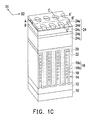
With reference to FIG. 1C , FIG. 2C , FIG. 3C , and FIG. 4C , a mask structure 24 is formed on the conductive material layer 22. The mask structure 24 includes a first advanced patterning film (APF) 24 a, a dielectric anti-reflective coating film (DARC) 24 b, a second advanced patterning film 24 c, a silicon-containing hard-mask bottom anti-reflection coating (SHB) 24 d, and a patterned photoresist layer 24 e in sequence. A material of the first advanced patterning film 24 a is amorphous carbon, for example. A material of the dielectric anti-reflective coating film 24 b is silicon oxynitride, for example. A material of the second advanced patterning film 24 c is amorphous carbon, for example. A material of the silicon-containing hard-mask bottom anti-reflection coating 24 d is an organosilicon polymer, polysilane, or a combination of the foregoing, for example. A material of the patterned photoresist layer 24 e is a positive photoresist, a negative photoresist, or a combination of the foregoing, for example. A thickness of the first advanced patterning film 24 a is in a range of 4000 Å to 15000 Å, for example. A thickness of the dielectric anti-reflective coating film 24 b is in a range of 300 Å to 2000 Å, for example. A thickness of the second advanced patterning film 24 c is in a range of 500 Å to 4000 Å, for example. A thickness of the silicon-containing hard-mask bottom anti-reflection coating 24 d is in a range of 200 Å to 1000 Å, for example. A thickness of the patterned photoresist layer 24 e is in a range of 200 Å to 3000 Å, for example. A method of forming the first advanced patterning film 24 a, the dielectric anti-reflective coating film 24 b, the second advanced patterning film 24 c, and the silicon-containing hard-mask bottom anti-reflection coating 24 d includes performing chemical vapor deposition, for example. A method of forming the patterned photoresist layer 24 e includes performing spin coating in combination with a lithography process, for example. In an embodiment, before forming the mask structure 24, a planarization process may be performed on the conductive material layer 22 to facilitate the subsequent patterning process.
With reference to FIG. 1C , FIG. 1D , FIG. 2D , FIG. 3D , and FIG. 4D , the conductive material layer 22 is patterned and a portion of the charge storage layer 18 and a portion of the dielectric layer 12 are removed by performing a non-selective etching process with the mask structure 24 as a mask, so as to form a mesh structure 26. The non-selective etching process means etching the conductive material layer 22, the charge storage layer 18, and the dielectric layer 12 at substantially the same etching rate. In an embodiment, an etching selectivity of the conductive material layer 22 to the charge storage layer 18 and an etching selectivity of the conductive material layer 22 to the dielectric layer 12 are respectively in a range of 0.7 to 1.3, for example. It should be noted that the aforementioned range of the etching selectivity is given as an example, and the invention is not limited thereto. The etching selectivity may be adjusted as required as long as the conductive material layer 22 on the sidewall of the opening for forming an isolating structure can be completely removed. The non-selective etching process is a dry etching process, for example. The dry etching process may be sputter etching, reactive ion etching, etc. In an embodiment, a gas used in the non-selective etching process is NF3, HBr, CH4, N2, He, Ar, SF6, CH2F2, and CH3F, for example.
With reference to FIG. 1D , FIG. 2D , FIG. 3D , and FIG. 4D , thereafter, the mask structure 24 is removed to expose the mesh structure 26. The mesh structure 26 includes a plurality of first strips 26 a and a plurality of second strips 26 b that intersect each other. Specifically, the first strips 26 a extend in a first direction D1 and are located at positions corresponding to the fin structures 14. That is, each first strip 26 a includes the fin structure 14 and a first strip conductive layer 25 a on the fin structure 14. The second strips 26 b extend in a second direction D2 and are located on the substrate 10. A second strip conductive layer 25 b of the second strip 26 b spans the fin structures 14. That is, each second strip 26 b includes a portion of the fin structure 14 and the second strip conductive layer 25 b spanning the fin structures 14. The first strip conductive layer 25 a and the second strip conductive layer 25 b are formed by patterning the conductive material layer 22 in FIG. 1C , FIG. 2C , FIG. 3C , and FIG. 4C . The first strip conductive layer 25 a and the second strip conductive layer 25 b intersect each other to form a mesh layer 25.
In other words, the mesh structure 26 has a plurality of holes P. The holes P are surrounded by the first strips 26 a and the second strips 26 b. The hole P is respectively located in the opening T between the adjacent two fin structures 14 (with reference to FIG. 1A and FIG. 1D ). The hole P extends into the dielectric layer 12 under the charge storage layer 18. That is to say, a bottom of the hole P is closer to the substrate 10 than a bottom of the fin structure 14. A method of removing the mask structure 24 includes performing dry etching, for example. The dry etching may be sputter etching, reactive ion etching, etc.
Since the mesh structure 26 is formed by the non-selective etching process, a residue of the conductive material layer 22 on the sidewall of the opening for forming the isolating structure is prevented or reduced effectively to avoid improper conduction between the semiconductor devices. Moreover, since the conductive material layer 22 is patterned to form the mesh layer 25, the structure has sufficient support in two directions, and thus collapse of the pattern is prevented.
With reference to FIG. 1C , FIG. 1D , FIG. 2D , FIG. 3D , and FIG. 4D , a distance between adjacent two holes P in the first direction D1 is in a range of 200 Å to 400 Å, for example. A distance between adjacent two holes P in the second direction D2 is in a range of 200 Å to 400 Å, for example. An area of the hole P is in a range of 5000 nm2 to 10000 nm2, for example. The hole P has a circular shape, a rectangular shape, a rhombic shape, or a combination of the foregoing, for example. It should be noted that the shape, area, and spacing of the holes P are given as examples, and the invention is not limited thereto. The holes P may have any shape, area, or distance therebetween as long as the conductive material layer 22 on the sidewall of the opening (i.e., the hole P) for forming the isolating structure can be completely removed.
With reference to FIG. 1C , FIG. 1D , FIG. 2D , FIG. 3D , and FIG. 4D , in an embodiment, a sidewall of each first strip 26 a is more oblique than a sidewall of each second strip 26 b. Specifically, a first angle A1 of each first strip 26 a may be smaller than a second angle A2 of each second strip 26 b. The first angle A1 is an angle between the sidewall of the first strip 26 a at the bottom of the hole P and the surface of the substrate 10. The second angle A2 is an angle between the sidewall of the second strip 26 b at the bottom of the hole P and the surface of the substrate 10.
With reference to FIG. 1D , FIG. 2D , FIG. 3D , and FIG. 4D , in the etching process, the etching is non-uniform due to a loading effect. As a result, the heights H3 of the sidewalls of the holes P formed in the mesh structure 26 may not be completely the same. However, since the holes P are filled with a dielectric material in the subsequent process, the different heights H3 of the holes P would not affect the overall electrical performance of the device. In an embodiment, the heights H3 of the sidewalls of the holes P in the mesh structure 26 differ from one another. In another embodiment, the height H3 of the sidewall of each hole P in the mesh structure 26 is greater than a height H of the first strip 26 a. For example, the height H3 of the sidewall of each hole P in the mesh structure 26 exceeds the height H of the first strip 26 a by 30% or more, or by 40% or more of the height H. In an embodiment, the height H3 of the sidewall of the hole P is in a range of 7000 Å to 12000 Å. The height H3 of the sidewall of each hole P in the mesh structure 26 exceeds the height H of the first strip 26 a by 1000 Å to 5000 Å, for example. By setting the height H3 of the sidewall of each hole P in the mesh structure 26 to exceed the height H of the first strip 26 a by 30% or more of the height H, it is ensured that the conductive material layer 22 on the sidewall of the opening for forming the isolating structure can be completely removed.
With reference to FIG. 1E , FIG. 2E , FIG. 3E , and FIG. 4E , then, a dielectric material layer 28 a is disposed to cover the mesh structure 26 and fill the holes P. A material of the dielectric material layer 28 a includes an oxide, a nitride, an oxy-nitride, or a low dielectric constant material having a dielectric constant smaller than 4. A thickness of the dielectric material layer 28 a on the mesh structure 26 is in a range of 200 Å to 1000 Å, for example. A method of forming the dielectric material layer 28 a includes performing chemical vapor deposition, for example.
With reference to FIG. 1D , FIG. 1E , FIG. 1F , FIG. 2F , FIG. 3F , and FIG. 4F , the dielectric material layer 28 a and the mesh structure 26 are patterned by performing a patterning process, such as lithography and etching processes, so as to form a plurality of comb structures 30 and dielectric pillars 28. Specifically, by performing the patterning process, cap layers 28 b on the surfaces of the second strips 26 b and the dielectric pillars 28 in the holes P are retained. The cap layers 28 b are located on a connection portion 30 b and extend in the second direction D2. Furthermore, by performing the patterning process, the first strips 26 a of the mesh structure 26 are partially removed, which leaves the comb structures 30. Each comb structure 30 includes a plurality of comb portions 30 a and the connection portion 30 b. Each comb portion 30 a is inserted into the opening T between the adjacent two fin structures 14 and is in contact with the sidewall of the charge storage layer 18 in the adjacent fin structures 14 (with reference to FIG. 1A and FIG. 1F ). The connection portion 30 b connects the comb portions 30 a and extends in the second direction D2. In an embodiment, a length of the connection portion 30 b in the first direction D1 in a range of 400 Å to 600 Å, for example. In an embodiment, a spacing between the connection portions 30 b is in a range of 200 Å to 400 Å, for example. In an embodiment, a length W1 of the connection portion 30 b in the first direction D1 is smaller than a length W2 of each dielectric rod 28 in the first direction D1.
In addition, when performing the patterning process, after formation of the cap layers 28 b and the comb structures 30, a portion of the fin structures 14 between the cap layers 28 b may be removed by performing an over etching process. Thus, the height (a first height H1) of each fin structure 14 between adjacent two comb structures 30 is smaller than the height (a second height H2) of each fin structure 14 under the comb structure 30. In an embodiment, the first height H1 is smaller than the second height H2 by 500 Å to 1000 Å. Owing to the loading effect, the conductive material between adjacent two comb structures 30 may not be removed completely. The steps of performing the over etching process and removing a portion of the fin structures 14 between the cap layers 28 b can prevent conduction between the adjacent two comb structures 30, caused by residual conductive material, after the patterning process.
With reference to FIG. 1F , FIG. 2F , FIG. 3F , and FIG. 4F , the semiconductor device of the invention includes the substrate 10, the dielectric layer 12, a plurality of fin structures 14, a plurality of comb structures 30, and a plurality of dielectric pillars 28. The dielectric layer 12 is located on the substrate 10. The fin structures 14 are located on the dielectric layer 12 and extend in the first direction D1. The fin structures 14 include the stack layer 16 and the charge storage layer 18. The stack layer 16 includes a plurality of conductive layers 16 a and a plurality of dielectric layers 16 b that are stacked alternately. The adjacent fin structures 14 have the opening T therebetween. The charge storage layer 18 covers the surfaces of the stack layer 16 and the dielectric layer 12.
With reference to FIG. 1F , FIG. 2F , FIG. 3F , and FIG. 4F , the comb structure 30 may be a conductive material. Each comb structure 30 includes a plurality of comb portions 30 a and the connection portion 30 b. The comb portion 30 a is inserted into the opening T between the adjacent two fin structures 14 and is in contact with the sidewall of the charge storage layer 18 in the adjacent fin structures 14. The connection portion 30 b extends in the second direction D2, and is located on the charge storage layer 18 and connects the comb portions 30 a.
The dielectric pillar 28 is inserted into the opening T between the adjacent two fin structures 14 and is in contact with the sidewalls of the adjacent fin structures 14 and the comb portion 30 a of the comb structure 30. In addition, the dielectric pillar 28 extends to a position closer to the substrate 10 than the fin structure 14 (that is, the dielectric pillar 28 extends into the dielectric layer 12 under the charge storage layer 18). The heights H3 of the dielectric pillars 28 may not be completely the same. In an embodiment, the heights H3 of the dielectric pillars 28 differ from one another. In another embodiment, the height H3 of each dielectric pillar 28 is greater than the height H1 of the fin structure 14. For example, the height H3 of each dielectric pillar 28 exceeds the height H1 of the fin structure 14 by 30% or more, or by 40% or more of the height H1.
In an embodiment, the sidewall of each fin structure 14 is more oblique than the sidewall of each comb portion 30 a. Specifically, the first angle A1 of each fin structure 14 (i.e., the charge storage layer 18) is smaller than the second angle A2 of each comb portion 30 a. The first angle A1 is an angle between the sidewall of each fin structure 14 and the surface of the substrate 10, and the second angle A2 is an angle between the sidewall of each comb portion 30 a and the surface of the substrate 10. The length W1 of each connection portion 30 b in the first direction D1 may be different from the length W2 of each dielectric pillar 28 in the first direction D1. In an embodiment, the length W1 of each connection portion 30 b in the first direction D1 is smaller than the length W2 of each dielectric pillar 28 in the first direction D1.
With reference to FIG. 1F , FIG. 2F , FIG. 3F , and FIG. 4F , the fin structures 14 may have different heights in the first direction D1. In an embodiment, the first height H1 of a portion of each fin structure 14 is smaller than the second height H2 of another portion of the fin structure 14. The first height H1 refers to a height of each fin structure 14 between the adjacent two comb structures 30. The second height H2 refers to a height of each fin structure 14 under the comb structure 30.
With reference to FIG. 1F , FIG. 2F , FIG. 3F , and FIG. 4F , the semiconductor device of the invention further includes a plurality of cap layers 28 b. The cap layer 28 b is located on the connection portion 30 b of the comb structure 30 and extends in the second direction D2.
In conclusion, according to the embodiment of the invention, a residue of the material layer that remains on the sidewall of the trench is removed effectively by performing the non-selective etching process and forming the mesh structure, thereby preventing improper conduction between the semiconductor devices. Moreover, since the conductive material layer is patterned into a mesh shape, the structure has sufficient support in two directions, and thus collapse of the pattern is prevented.
It will be apparent to those skilled in the art that various modifications and variations can be made to the disclosed embodiments without departing from the scope or spirit of the invention. In view of the foregoing, it is intended that the invention covers modifications and variations provided that they fall within the scope of the following claims and their equivalents.
Claims (9)
1. A semiconductor device, comprising:
a substrate;
a plurality of fin structures located on the substrate and extending in a first direction, wherein the adjacent fin structures have an opening therebetween;
a plurality of comb structures comprising a conductive material, wherein each of the comb structures comprises:
a plurality of comb portions respectively inserted into the opening between the adjacent fin structures and in contact with sidewalls of the adjacent fin structures; and
a connection portion extending in a second direction and located on the fin structures to connect the comb portions; and
a plurality of dielectric pillars respectively inserted into the opening between the adjacent fin structures and in contact with the sidewalls of the adjacent fin structures and the comb portions, wherein the dielectric pillars extend to positions closer to the substrate than bottoms of the fin structures.
2. The semiconductor device according to claim 1 , wherein the fin structures respectively comprise a stack layer and a charge storage layer, wherein the stack layer comprises at least one conductive layer and at least one dielectric layer stacked alternately, and the charge storage layer covers the substrate at a bottom of the opening and a surface of the stack layer.
3. The semiconductor device according to claim 1 , wherein a first angle of the fin structures is smaller than a second angle of the comb portions, wherein the first angle is an angle between the sidewall of the fin structure and the surface of the substrate, and the second angle is an angle between a sidewall of the comb portion and the surface of the substrate.
4. The semiconductor device according to claim 1 , wherein the dielectric pillars have different heights.
5. The semiconductor device according to claim 1 , wherein the height of each dielectric pillar is greater than a height of each fin structure.
6. The semiconductor device according to claim 5 , wherein the height of each dielectric pillar exceeds the height of each fin structure by 30% or more of the height of the fin structure.
7. The semiconductor device according to claim 1 , wherein a length of the connection portion in the first direction is smaller than a length of each dielectric pillar in the first direction.
8. The semiconductor device according to claim 1 , wherein a first height of a portion of each fin structure is smaller than a second height of another portion of the fin structure, wherein the first height is a height of each fin structure between the adjacent comb structures, and the second height is a height of each fin structure under the comb structure.
9. The semiconductor device according to claim 2 , further comprising: a plurality of cap layers located on the connection portion and extending in the second direction, and wherein the stack layer is stacked in a third direction which is perpendicular to the first direction.
Priority Applications (1)
| Application Number | Priority Date | Filing Date | Title |
|---|---|---|---|
| US14/733,508 US9553104B2 (en) | 2015-06-08 | 2015-06-08 | Semiconductor device and method of fabricating the same |
Applications Claiming Priority (1)
| Application Number | Priority Date | Filing Date | Title |
|---|---|---|---|
| US14/733,508 US9553104B2 (en) | 2015-06-08 | 2015-06-08 | Semiconductor device and method of fabricating the same |
Publications (2)
| Publication Number | Publication Date |
|---|---|
| US20160358934A1 US20160358934A1 (en) | 2016-12-08 |
| US9553104B2 true US9553104B2 (en) | 2017-01-24 |
Family
ID=57452121
Family Applications (1)
| Application Number | Title | Priority Date | Filing Date |
|---|---|---|---|
| US14/733,508 Active US9553104B2 (en) | 2015-06-08 | 2015-06-08 | Semiconductor device and method of fabricating the same |
Country Status (1)
| Country | Link |
|---|---|
| US (1) | US9553104B2 (en) |
Families Citing this family (7)
| Publication number | Priority date | Publication date | Assignee | Title |
|---|---|---|---|---|
| US11120884B2 (en) | 2015-09-30 | 2021-09-14 | Sunrise Memory Corporation | Implementing logic function and generating analog signals using NOR memory strings |
| US9842651B2 (en) | 2015-11-25 | 2017-12-12 | Sunrise Memory Corporation | Three-dimensional vertical NOR flash thin film transistor strings |
| US10475812B2 (en) | 2018-02-02 | 2019-11-12 | Sunrise Memory Corporation | Three-dimensional vertical NOR flash thin-film transistor strings |
| US11282855B2 (en) * | 2018-12-07 | 2022-03-22 | Sunrise Memory Corporation | Methods for forming multi-layer vertical NOR-type memory string arrays |
| WO2021127218A1 (en) | 2019-12-19 | 2021-06-24 | Sunrise Memory Corporation | Process for preparing a channel region of a thin-film transistor |
| WO2022108848A1 (en) | 2020-11-17 | 2022-05-27 | Sunrise Memory Corporation | Methods for reducing disturb errors by refreshing data alongside programming or erase operations |
| TW202310429A (en) | 2021-07-16 | 2023-03-01 | 美商日升存儲公司 | 3-dimensional memory string array of thin-film ferroelectric transistors |
Citations (2)
| Publication number | Priority date | Publication date | Assignee | Title |
|---|---|---|---|---|
| US8664761B1 (en) * | 2012-12-21 | 2014-03-04 | Macronix International Co., Ltd. | Semiconductor structure and manufacturing method of the same |
| US20140273372A1 (en) * | 2013-03-15 | 2014-09-18 | Kabushiki Kaisha Toshiba | Method of manufacturing nonvolatile semiconductor memory device |
-
2015
- 2015-06-08 US US14/733,508 patent/US9553104B2/en active Active
Patent Citations (2)
| Publication number | Priority date | Publication date | Assignee | Title |
|---|---|---|---|---|
| US8664761B1 (en) * | 2012-12-21 | 2014-03-04 | Macronix International Co., Ltd. | Semiconductor structure and manufacturing method of the same |
| US20140273372A1 (en) * | 2013-03-15 | 2014-09-18 | Kabushiki Kaisha Toshiba | Method of manufacturing nonvolatile semiconductor memory device |
Also Published As
| Publication number | Publication date |
|---|---|
| US20160358934A1 (en) | 2016-12-08 |
Similar Documents
| Publication | Publication Date | Title |
|---|---|---|
| US9553104B2 (en) | Semiconductor device and method of fabricating the same | |
| US11758736B2 (en) | Ferroelectric random access memory devices and methods | |
| US8603919B2 (en) | Method for fabricating semiconductor device | |
| KR101671464B1 (en) | Method for manufacturing a semiconductor device | |
| CN110875285B (en) | Semiconductor structure and forming method thereof | |
| US20170170272A1 (en) | Cointegration of directed self assembly and sidewall image transfer patterning for sublithographic patterning with improved design flexibility | |
| US20150243503A1 (en) | Stacked sidewall patterning | |
| US9812575B1 (en) | Contact formation for stacked FinFETs | |
| KR20100059680A (en) | Method for manufacturing semiconductor device | |
| TW201913753A (en) | Fin field effect transistor (finfet) device structure and method for forming the same | |
| US20230326990A1 (en) | Multi-Channel Devices and Methods of Manufacture | |
| CN111199880B (en) | Manufacturing method of semiconductor device and semiconductor device | |
| US20160300849A1 (en) | Semiconductor device and method of fabricating the same | |
| US10600687B2 (en) | Process integration techniques using a carbon layer to form self-aligned structures | |
| CN101339902B (en) | high-voltage semiconductor device and method of fabricating semiconductor high-voltage device | |
| KR20210051275A (en) | Vertical memory devices | |
| US9324789B1 (en) | Memory device and method for fabricating the same | |
| TWI549227B (en) | Memory device and method for fabricating the same | |
| US11145760B2 (en) | Structure having improved fin critical dimension control | |
| US9337209B1 (en) | Semiconductor device and method of fabricating the same | |
| TWI547983B (en) | Semiconductor device and method of fabricating the same | |
| US20160086968A1 (en) | Semiconductor device | |
| US9343477B2 (en) | Semiconductor device and method for fabricating the same | |
| CN106298497B (en) | Semiconductor element and its manufacturing method | |
| TWI559446B (en) | Semiconductor device and method of fabricating the same |
Legal Events
| Date | Code | Title | Description |
|---|---|---|---|
| AS | Assignment |
Owner name: MACRONIX INTERNATIONAL CO., LTD., TAIWAN Free format text: ASSIGNMENT OF ASSIGNORS INTEREST;ASSIGNOR:LIN, LO-YUEH;REEL/FRAME:035804/0415 Effective date: 20150528 |
|
| STCF | Information on status: patent grant |
Free format text: PATENTED CASE |
|
| MAFP | Maintenance fee payment |
Free format text: PAYMENT OF MAINTENANCE FEE, 4TH YEAR, LARGE ENTITY (ORIGINAL EVENT CODE: M1551); ENTITY STATUS OF PATENT OWNER: LARGE ENTITY Year of fee payment: 4 |