US9552766B2 - Electroluminescence display device with light emission control and driving method thereof - Google Patents
Electroluminescence display device with light emission control and driving method thereof Download PDFInfo
- Publication number
- US9552766B2 US9552766B2 US14/468,514 US201414468514A US9552766B2 US 9552766 B2 US9552766 B2 US 9552766B2 US 201414468514 A US201414468514 A US 201414468514A US 9552766 B2 US9552766 B2 US 9552766B2
- Authority
- US
- United States
- Prior art keywords
- period
- gray scale
- duty
- light
- control
- Prior art date
- Legal status (The legal status is an assumption and is not a legal conclusion. Google has not performed a legal analysis and makes no representation as to the accuracy of the status listed.)
- Expired - Fee Related, expires
Links
- 238000005401 electroluminescence Methods 0.000 title claims abstract description 104
- 238000000034 method Methods 0.000 title claims description 25
- 239000011159 matrix material Substances 0.000 claims description 12
- 238000005070 sampling Methods 0.000 claims description 4
- 238000012937 correction Methods 0.000 description 21
- 230000007423 decrease Effects 0.000 description 11
- 230000006866 deterioration Effects 0.000 description 7
- 238000012545 processing Methods 0.000 description 7
- 238000013459 approach Methods 0.000 description 5
- 238000010586 diagram Methods 0.000 description 5
- 230000015556 catabolic process Effects 0.000 description 3
- 238000006731 degradation reaction Methods 0.000 description 3
- 239000000758 substrate Substances 0.000 description 2
- 241001270131 Agaricus moelleri Species 0.000 description 1
- 230000002411 adverse Effects 0.000 description 1
- 238000007599 discharging Methods 0.000 description 1
- 238000012552 review Methods 0.000 description 1
- 239000010409 thin film Substances 0.000 description 1
Images


Classifications
-
- G—PHYSICS
- G09—EDUCATION; CRYPTOGRAPHY; DISPLAY; ADVERTISING; SEALS
- G09G—ARRANGEMENTS OR CIRCUITS FOR CONTROL OF INDICATING DEVICES USING STATIC MEANS TO PRESENT VARIABLE INFORMATION
- G09G3/00—Control arrangements or circuits, of interest only in connection with visual indicators other than cathode-ray tubes
- G09G3/20—Control arrangements or circuits, of interest only in connection with visual indicators other than cathode-ray tubes for presentation of an assembly of a number of characters, e.g. a page, by composing the assembly by combination of individual elements arranged in a matrix no fixed position being assigned to or needed to be assigned to the individual characters or partial characters
- G09G3/22—Control arrangements or circuits, of interest only in connection with visual indicators other than cathode-ray tubes for presentation of an assembly of a number of characters, e.g. a page, by composing the assembly by combination of individual elements arranged in a matrix no fixed position being assigned to or needed to be assigned to the individual characters or partial characters using controlled light sources
- G09G3/30—Control arrangements or circuits, of interest only in connection with visual indicators other than cathode-ray tubes for presentation of an assembly of a number of characters, e.g. a page, by composing the assembly by combination of individual elements arranged in a matrix no fixed position being assigned to or needed to be assigned to the individual characters or partial characters using controlled light sources using electroluminescent panels
- G09G3/32—Control arrangements or circuits, of interest only in connection with visual indicators other than cathode-ray tubes for presentation of an assembly of a number of characters, e.g. a page, by composing the assembly by combination of individual elements arranged in a matrix no fixed position being assigned to or needed to be assigned to the individual characters or partial characters using controlled light sources using electroluminescent panels semiconductive, e.g. using light-emitting diodes [LED]
- G09G3/3208—Control arrangements or circuits, of interest only in connection with visual indicators other than cathode-ray tubes for presentation of an assembly of a number of characters, e.g. a page, by composing the assembly by combination of individual elements arranged in a matrix no fixed position being assigned to or needed to be assigned to the individual characters or partial characters using controlled light sources using electroluminescent panels semiconductive, e.g. using light-emitting diodes [LED] organic, e.g. using organic light-emitting diodes [OLED]
- G09G3/3225—Control arrangements or circuits, of interest only in connection with visual indicators other than cathode-ray tubes for presentation of an assembly of a number of characters, e.g. a page, by composing the assembly by combination of individual elements arranged in a matrix no fixed position being assigned to or needed to be assigned to the individual characters or partial characters using controlled light sources using electroluminescent panels semiconductive, e.g. using light-emitting diodes [LED] organic, e.g. using organic light-emitting diodes [OLED] using an active matrix
- G09G3/3233—Control arrangements or circuits, of interest only in connection with visual indicators other than cathode-ray tubes for presentation of an assembly of a number of characters, e.g. a page, by composing the assembly by combination of individual elements arranged in a matrix no fixed position being assigned to or needed to be assigned to the individual characters or partial characters using controlled light sources using electroluminescent panels semiconductive, e.g. using light-emitting diodes [LED] organic, e.g. using organic light-emitting diodes [OLED] using an active matrix with pixel circuitry controlling the current through the light-emitting element
-
- G—PHYSICS
- G09—EDUCATION; CRYPTOGRAPHY; DISPLAY; ADVERTISING; SEALS
- G09G—ARRANGEMENTS OR CIRCUITS FOR CONTROL OF INDICATING DEVICES USING STATIC MEANS TO PRESENT VARIABLE INFORMATION
- G09G2300/00—Aspects of the constitution of display devices
- G09G2300/08—Active matrix structure, i.e. with use of active elements, inclusive of non-linear two terminal elements, in the pixels together with light emitting or modulating elements
- G09G2300/0809—Several active elements per pixel in active matrix panels
- G09G2300/0842—Several active elements per pixel in active matrix panels forming a memory circuit, e.g. a dynamic memory with one capacitor
- G09G2300/0861—Several active elements per pixel in active matrix panels forming a memory circuit, e.g. a dynamic memory with one capacitor with additional control of the display period without amending the charge stored in a pixel memory, e.g. by means of additional select electrodes
Definitions
- One or more embodiments described herein relate to an electroluminescence display device and method of driving such a device.
- One type of display device uses electroluminescence (EL) light-emitting elements to generate images.
- EL electroluminescence
- Each EL element generates light based on a supplied current.
- the luminance of light tends to vary based on the transistor characteristics of each pixel. For example, variations in the threshold voltage of the driving transistor of each pixel may cause differences in luminance, which adversely affects display quality.
- an electroluminescence display device includes a plurality of pixel circuits, each of the pixel circuits including a light-emitting element to emit light based on a supplied current, a driving transistor to supply the current to the light-emitting element based on a potential of a gate terminal of the driving transistor, a sampling switch to sample a data voltage corresponding to image data at the gate terminal of the driving transistor, a switch transistor to place the driving transistor in a diode-connected state, and a capacitive element to store a potential of the gate terminal of the driving transistor.
- One vertical period in which each of the pixel circuits is driven includes a current gray scale control period and a duty gray scale control period, in the current gray scale control period the current to be supplied to the light-emitting element is controlled based on the data voltage, and in the duty gray scale control period a supplying period of the current provided to the light-emitting element is controlled based on a duty control voltage.
- the data voltage and the duty control voltage are supplied to a source terminal of the driving transistor in the driving transistor diode-connected state.
- the duty control voltage has two voltage values.
- the supplying period of the current provided to the light-emitting element when each of the pixel circuits is driven at a first gray scale value is longer than that when each pixel circuit is driven at a second gray scale, the first gray scale value being greater than the second gray scale value.
- the device may include a plurality of control lines arranged in a row direction, the control lines to supply control signals for controlling transistors in respective ones of the pixel circuits; and a plurality of signal lines arranged in a column direction, the signal lines to supply data voltages and duty control voltages to respective ones of the pixel circuits.
- the pixel circuits may be arranged in a matrix and are connected to corresponding control lines and corresponding signal lines. Operations which include initializing the gate terminal of the driving transistor and the potential of the capacitive element, correcting a threshold voltage of the driving transistor, programming data at the gate terminal of the driving transistor, and controlling a duty period of the driving transistor may be line-sequentially performed for each of the pixel circuits. A light-emitting timing and a non-light-emitting timing of the light-emitting element may be different for the pixel circuits.
- the device may include a plurality of control lines arranged in a row direction, the control lines to supply control signals for controlling transistors in respective ones of the pixel circuits; and a plurality of signal lines arranged in a column direction, the signal lines to supply data voltages and duty control voltages to respective ones of the pixel circuits.
- the pixel circuits may be arranged in a matrix form and are connected to corresponding control lines and corresponding signal lines. Operations which include initializing the gate terminal of the driving transistor and the potential of the capacitive element and correcting a threshold voltage of the driving transistor are simultaneously performed for each of the pixel circuits, and operations of programming data at the gate terminal of the driving transistor and controlling a duty period of the driving transistor may be line-sequentially performed for each of the pixel circuits. A light-emitting timing and a non-light-emitting timing of the light-emitting element may be different for the pixel circuits.
- the current gray scale control period may be substantially equal to the duty gray scale control period.
- the duty gray scale control period may include a plurality of sub-frames, and the supplying period of the current provided to the light-emitting element based on the duty control voltage may be controlled every sub-frame.
- the current gray scale control period may be substantially equal to a period of each sub-frame of the duty gray scale control period.
- a method for driving an electroluminescence display device includes controlling a current for a light-emitting element based on a data voltage and a supplying period of a current for the light-emitting element based on a duty control voltage, during one vertical period in which at least one pixel circuit is driven; and supplying the data voltage and the duty control voltage to a source terminal of a driving transistor of the at least one pixel circuit when the driving transistor is in a diode-connected state, wherein the duty control voltage has two voltage values, and wherein the supplying period of the current for the light-emitting element when the at least one pixel circuit is driven at a first gray scale value is longer than the supplying period when the at least one pixel circuit is driven at a second gray scale value less than the first gray scale value.
- One vertical period in which each of the pixel circuits is driven may include a current gray scale control period and a duty gray scale control period, in the current gray scale control period the current to be supplied to the light-emitting element may be controlled based on the data voltage, and in the duty gray scale control period a supplying period of the current provided to the light-emitting element may be controlled based on a duty control voltage.
- the method may include supplying control signals for controlling transistors of a plurality of pixel circuits; and supplying data voltages and duty control voltages to the pixel circuits, the pixel circuits arranged in a matrix and connected to corresponding control lines and corresponding signal lines.
- the method may further include line-sequentially performing operations which include initializing a gate terminal of the driving transistor and a potential of the capacitive element, correcting a threshold voltage of the driving transistor, programming data at the gate terminal of the driving transistor, and controlling a duty period of the driving transistor for each of the pixel circuits, wherein a light-emitting timing and a non-light-emitting timing of light-emitting elements of the pixel circuits are different.
- the method may include supplying control signals for controlling transistors in a plurality of pixel circuits; and supplying the data voltage and the duty control voltage to each of the pixel circuits, the pixel circuits arranged in a matrix and connected to corresponding control lines and corresponding signal lines.
- the method may further include simultaneously performing operations which include initializing the gate terminal of the driving transistor and the potential of the capacitive element and correcting a threshold voltage of the driving transistor for each of the pixel circuits, and line-sequentially performing operations which include programming data at the gate terminal of the driving transistor and controlling a duty period of the driving transistor for each of the pixel circuits, wherein a light-emitting timing and a non-light-emitting timing of the light-emitting element are different for the pixel circuits.
- the current gray scale control period may be substantially equal to the duty gray scale control period.
- the duty gray scale control period may includes a plurality of sub-frames, and the supplying period of the current provided to the light-emitting element based on the duty control voltage may be controlled every sub-frame.
- the current gray scale control period may be substantially equal to a period of each sub-frame of the duty gray scale control period.
- an apparatus in accordance with another embodiment, includes an interface and a controller coupled to the interface, the controller to control at least one pixel circuit during a first period and a second period, wherein the controller is to control current to a light-emitting element of the at least one pixel circuit based on a data voltage in the first period, wherein the controller is to control a supplying period of current to the light-emitting element based on a duty control voltage in the second period, and wherein the supplying period when the pixel circuit is driven at a first gray scale value is longer than that when the pixel circuit is driven at a second gray scale, the first gray scale value being greater than the second gray scale value.
- the data voltage and the duty control voltage may be supplied to a source terminal of a driving transistor of the pixel circuit when the driving transistor is in a diode-connected state.
- the first period may be substantially equal to the second period.
- the first period may be substantially equal to a period of a sub-frame in the second period.
- the controller may line-sequentially control operations which include initializing a gate terminal of a driving transistor and a potential of a capacitive element of the at least one pixel circuit, correcting a threshold voltage of the driving transistor, programming data at the gate terminal of the driving transistor, and controlling a duty period of the driving transistor.
- the at least one pixel circuit may include a plurality of pixel circuits, and a light-emitting timing and a non-light-emitting timing may be different for the pixel circuits.
- the controller may simultaneously control operations which include initializing a gate terminal of a driving transistor and a potential of a capacitive element, and correcting a threshold voltage of the driving transistor of each of a plurality of pixel circuits.
- the controller may line-sequentially control operations which include programming data at the gate terminal of the driving transistor and controlling a duty period of the driving transistor of each of the pixel circuits.
- the second period may include a plurality of sub-frames, and the supplying period of the current to the light-emitting element based on the duty control voltage may be controlled every sub-frame.
- FIG. 1 illustrates an embodiment of an EL display device
- FIG. 2 illustrates an embodiment of a pixel circuit
- FIG. 3 illustrates an example of how the EL display device operates
- FIG. 4 illustrates an example of control signals for the EL display device
- FIG. 5 illustrates an example of more control signals for the EL display device
- FIGS. 6A-6D illustrate different operating states of the pixel circuit
- FIG. 7 illustrates an example of a duty control program
- FIG. 8 illustrates an example of another duty control program
- FIG. 9 illustrates an example of EL current and luminance
- FIG. 10 illustrates an example of EL current and gray scale
- FIG. 11 illustrates another example of how an EL display device operates
- FIG. 12 illustrates an example of control signals for pixel circuits
- FIG. 13 illustrates another example of EL current and luminance
- FIG. 14 illustrates another example of EL current and gray scale
- FIG. 15 illustrates another embodiment of an EL display device
- FIG. 16 illustrates another example of how an EL display device operates
- FIG. 17 illustrates another example of control signals for a pixel circuit
- FIG. 18 illustrates another example of control signals for pixel circuits
- FIGS. 19A-19F illustrate different operating states of a pixel circuit.
- FIG. 1 illustrates an embodiment of an electroluminescence (EL) display device 500 which may be used as a display unit of an electronic device, such as but not limited to a television, a smart phone, a handheld telephone, and a personal computer.
- the EL display device 500 includes a plurality of pixel circuits 100 arranged in a matrix and a controller 505 which includes an initialization control driver 510 , a scan driver 530 , and an emission driver 550 .
- the controller 505 generates signals for controlling the pixel circuits 100 .
- the signals are sent through an interface, which, for example, may be one or more outputs of a chip including the controller or the signal lines to be discussed in greater detail below.
- the EL display device 500 displays images through light-emitting elements (EL element) in the pixel circuits 100 .
- each EL element may be an organic EL element such as an organic light-emitting diode (OLED).
- OLED organic light-emitting diode
- the EL element may be different from an OLED, e.g., one having a rectification characteristic.
- the pixel circuits 100 are connected to signal lines DT that provide image data.
- the pixel circuits 100 extend in a column direction and are also connected to power lines GL that provide a power supply voltage ELVDD to the pixel circuits 100 for light-emission.
- the power lines GL also extend in the column direction. Lower ends of the power lines GL are commonly connected to receive the power supply voltage ELVDD.
- the pixel circuits 100 are arranged in n rows and m columns (e.g., an n ⁇ m matrix). The pixel circuits 100 are connected to corresponding signal lines DT and corresponding power lines GL.
- Control lines SIL extend in a row direction and are connected to the initialization control driver 510 .
- Scan lines SCL extend in the row direction and are connected to the scan driver 530 .
- Light-emitting control lines EML extend in the row direction and are connected to the emission driver 550 .
- Initialization voltage lines VIL also extend in the row direction. First ends of the initialization voltage lines VIL are commonly connected.
- the pixel circuits 100 are connected to corresponding control lines SIL, scan lines SCL, light-emitting control lines EML, and initialization voltage lines VIL by on a row-by-row basis. Transistors in the pixel circuits 100 are controlled by control signals from the control lines SIL, scan lines SCL, and light-emitting control lines EML.
- the initialization control driver 510 outputs initialization control signals INIT through the control lines SIL.
- the scan driver 530 outputs scan signals SCAN through the scan lines SCL.
- the emission driver 550 outputs light-emitting control signals EM through the light-emitting control lines EML.
- the initialization voltage lines VIL receive an initialization voltage VINIT in common.
- the EL display device 500 may include a control unit and a power supply unit.
- the control unit may including a central processing unit (CPU) or other processing device, a memory, and so on, for controlling operations of the EL display device 500 .
- the control unit may control the initialization control driver 510 , the scan driver 530 , and the emission driver 550 .
- the control unit may also provide the pixel circuits 100 with data voltages and duty control voltages through the signal lines DT.
- the power supply unit supplies power to the EL display device 500 and, optionally, various components of an electronic device which includes the EL display device 500 .
- the power supply unit may supply the EL element of each pixel circuit 100 with an anode voltage ELVDD and a cathode voltage ELVSS.
- FIG. 2 illustrates an embodiment of a pixel circuit, which, for example, may correspond to the pixel circuits 100 in the EL display device of FIG. 1 .
- the pixel circuit 100 includes a driving transistor M 1 , a sampling switch M 2 , switch transistors M 3 , M 4 , M 5 , and M 6 , a capacitive element Cst, and an EL element.
- each transistor is a p-type thin film transistor.
- the driving transistor M 1 supplies current to the EL element according to the potential of a gate terminal of the driving transistor M 1 .
- the sampling transistor M 2 samples a data voltage corresponding to image data at the gate terminal of the driving transistor M 1 .
- the switch transistor M 5 is used to place the driving transistor M 1 in a diode-connected state.
- the capacitive element Cst holds the potential of the gate terminal of the driving transistor M 1 .
- the EL element emits light according to the supplied current.
- One terminal of the switch transistor M 6 is connected to an initialization voltage line VIL. Another terminal of the switch transistor M 6 is connected to the gate terminal of the driving transistor M 1 and the capacitive element Cst.
- the switch transistor M 6 is controlled by an initialization control signal INIT, which is provided to the gate terminal of the switch transistor M 6 .
- the switch transistor M 6 that is controlled by the initialization control signal INIT, initializes the gate terminal of the driving transistor M 1 and a potential of the capacitive element Cst with an initialization voltage VINIT.
- One terminal of the switch transistor M 2 is connected to a signal line DT supplied with a data voltage VDATA or a duty control voltage VDUTY, and the other terminal thereof is connected to a source terminal of the driving transistor M 1 .
- One terminal of the switch transistor M 3 is connected to the power line GL supplied with a power supply voltage ELVDD, and the other terminal thereof is connected to the source terminal of the driving transistor M 1 .
- a gate terminal of the switch transistor M 2 is connected to the scan line SCL.
- the switch transistor M 2 is controlled by a scan signal SCAN supplied to the gate terminal of the switch transistor M 2 via the scan line SCL.
- the gate terminal of the switch transistor M 3 is connected to the light-emitting control line EML.
- the switch transistor M 3 is controlled by the light-emitting control signal EM, which is provided to the gate terminal of the switch transistor M 3 via a light-emitting control line EML.
- the switch transistor M 2 provides the source terminal of the driving transistor M 1 with one of the data voltage VDATA or the duty control voltage VDUTY.
- the power supply voltage ELVDD is provided to the source terminal of the driving transistor M 1 via the switch transistor M 3 .
- the gate terminal of the switch transistor M 5 is connected to the scan line SCL.
- the switch transistor M 5 is controlled by a scan signal SCAN, which is provided to the gate terminal of the switch transistor M 5 via the scan line SCL.
- One terminal of the switch transistor M 4 is connected to the drain terminal of the driving transistor M 1 , and another terminal thereof is connected to the EL element.
- a gate terminal of the switch transistor M 4 is connected to the light-emitting control line EML.
- the switch transistor M 4 is controlled by the light-emitting control signal EM, which is provided to the gate terminal of the switch transistor M 4 via the light-emitting control line EML.
- FIG. 3 is an example of a timing diagram illustrating operation of the EL display device 500 .
- one vertical period includes a current gray scale control period and a duty gray scale control period.
- the current gray scale control period data voltages VDATA corresponding to image data are programmed at the pixel circuits 100 line-sequentially, to thereby control the current to be supplied to EL elements.
- the duty control voltage VDUTY is used to stop the pixel circuits 100 from emitting light or to continue to emit light, e.g., maintain a sampled data voltage according to a current gray scale control way.
- a period in which current is supplied to the EL element is adjusted.
- light-emission from the pixel circuits 100 is interrupted at one or more low gray scale values and is made at one or more high gray scales.
- the EL display device 500 uses current gray scale control and duty gray scale control to control gray scale values of the pixel circuits 100 .
- FIG. 4 is an example of another timing diagram for controlling operation of a unit pixel circuit.
- FIG. 5 is an example of another timing diagram for controlling operation of pixel circuits in rows.
- the pixel circuit(s) may be pixel circuits 100 .
- a method for driving the EL display device 500 is performed based on an initialization period (a), a threshold voltage (VTH) correction and data programming period (b), a duty control period (c), and a light-emitting period (d).
- the pixel circuits 100 may be line-sequentially controlled by control signals INIT, SCAN, and EM.
- Current gray scale control and duty gray scale control based on image data are performed with respect to each pixel circuit 100 , using a data voltage VDATA and a duty control voltage VDUTY that are provided to a source terminal of a driving transistor M 1 via a signal line DT.
- the gray scale value of light emitted from each pixel circuit 100 may depend on a sum of current provided to an EL element in the current gray scale control period and current provided to the EL element in the duty gray scale control period.
- the current gray scale control period and the duty gray scale control period may be set to the same time, to thereby simplifying gray scale control. In other embodiments, these periods may be set to different times. The above-described control periods will be more fully described with reference to FIGS. 6A-6D .
- FIGS. 6A to 6D illustrate different operating states of a pixel circuit, e.g., pixel circuit 100 .
- the switch transistor M 6 is turned on by the initialization control signal INIT.
- the initialization voltage VINIT is provided to the gate terminal of the driving transistor M 1 and the capacitive element Cst through the switch transistor M 6 .
- the gate terminal of the driving transistor M 1 and the potential of the capacitive element Cst are initialized based on the initialization voltage VINIT.
- the switch transistor M 6 is turned off and the switch transistors M 2 and M 5 are turned on by a scan signal SCAN.
- the data line DT receives the data voltage VDATA, and the driving transistor M 1 is diode-connected through the switch transistor M 5 .
- the data voltage VDATA corresponding to image data is provided to the source terminal of the driving transistor M 1 .
- the capacitive element Cst samples a voltage of (VDATA ⁇ VTH), where VTH is the threshold voltage of the driving transistor M 1 .
- the signal line DT receives the duty control voltage VDUTY.
- the duty control voltage VDUTY has two voltage values.
- the two voltage values of the duty control voltage VDUTY are provided to the source terminal of the driving transistor M 1 according to display gray scale, such that light-emitting halt (high level) and light-emitting continuance (low level) of the pixel circuit 100 are performed.
- the switch transistors M 2 and M 5 are turned off by the scan signal SCAN, and the switch transistors M 3 and M 4 are turned on by the light-emitting control signal EM.
- Current controlled by the driving transistor M 1 is provided to the EL element. That is, light-emitting of the pixel circuit 100 is controlled.
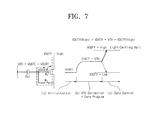
- FIG. 7 illustrates an example of a duty control program 1
- FIG. 8 illustrates an example of a duty control program 2 .
- the driving transistor M 1 may be programmed in one direction corresponding to a charging direction (or, a discharging direction) due to its diode characteristic. That is, when VTH correction on the diode-connected driving transistor M 1 is performed, the driving transistor M 1 is turned off but cannot be turned on when a voltage is supplied to a source terminal of the driving transistor M 1 .
- Two voltage values of a duty control voltage VDUTY may be set to be higher than the lowest gray scale voltage (e.g., dark) and to be lower than the highest gray scale voltage (e.g., bright).
- a light-emitting halt operation and a light-emitting continuance operation are performing using the two voltage values.
- the source terminal of a driving transistor M 1 where a voltage of (VDATA ⁇ VTH) is sampled after initialization, is supplied with a duty control voltage VDUTY (high level) greater than (VDATA ⁇ VTH).
- VDUTY high level
- VDATA ⁇ VTH the driving transistor M 1 is turned off because the gate voltage of the driving transistor M 1 is overwritten with the duty control voltage VDUTY at the high level.
- the supply of current to the EL element is stopped during the light-emitting period, and the EL element does not emit light even though the switch transistor M 4 is turned on.
- the source terminal of the driving transistor M 1 where a voltage of (VDATA ⁇ VTH) is sampled after initialization, is supplied with a duty control voltage VDUTY (low level) lower than (VDATA ⁇ VTH).
- VDATA ⁇ VTH a duty control voltage lower than (VDATA ⁇ VTH)
- the gate voltage of the driving transistor M 1 is (VDATA ⁇ VTH), because it is not overwritten with the duty control voltage VDUTY at the low level.
- FIG. 9 illustrates an example of a relationship between EL current and luminance
- FIG. 10 illustrates an example of a relationship between EL current and gray scale.
- the relationship between the EL current and the gray scale corresponds to a gamma curve.
- the light-emitting duty period (e.g., a period where current flows into the EL element) varies with gray scale value.
- the light-emitting duty period at a high gray scale value e.g., bright
- a low gray scale value e.g., dark
- the current flowing into the EL element decreases. This causes a deterioration in image quality due to variation in the threshold voltage VTH, thereby resulting in non-uniform luminance.
- the light-emitting duty period is controlled to decrease and current to be provided to the EL element is controlled to increase. Thus, it is possible to suppress deterioration of image quality due to threshold voltage VTH variation.
- the luminance of the EL element deteriorates when a maximum current is provided to the EL element increases.
- the light-emitting duty period is controlled to increase and the maximum current provided to the EL element is controlled to be suppressed, e.g., reduce.
- the useful life time of the EL element it is possible to make the useful life time of the EL element longer.
- the pixel circuit 100 when the pixel circuit 100 is driven at a high gray scale value, it is desirable to suppress (reduce) the maximum current to be supplied to the EL element. However, when the pixel circuit 100 is driven at a low gray scale value, it is desirable to increase the intensity of current in order to suppress variation in the threshold voltage VTH. This operation may be performed through duty control.
- FIG. 11 another example of how an EL display device operates
- FIG. 12 is another example of a timing diagram for controlling operation of pixel circuits, e.g., pixel circuits 100 .
- the duty gray scale control period includes a plurality of sub-frames. A period where current is provided to the EL element according to a duty control voltage VDUTY is controlled on a sub-frame basis. Also, the current gray scale control period and a period of each sub-frame of the duty gray scale control period are set to be equal to each other.
- one vertical period includes a current gray scale control period and a duty gray scale control period.
- the duty gray scale control period includes a plurality of sub-frames, and duty gray scale control is performed every sub-frame.
- data voltages VDATA corresponding to image data are line-sequentially programmed at the pixel circuits 100 , such that current to be provided to EL elements is controlled.
- the duty gray scale control period having a plurality of sub-frames a period where current is provided to the EL element is controlled by making the pixel circuits 100 stop emitting light or continue emitting light according to a duty control voltage VDUTY every sub-frame.
- he light-emitting duty period is controlled to decrease when the pixel circuit 100 is driven at a low gray scale value.
- the pixel circuit 100 may not emit light until data is programmed again.
- the pixel circuit 100 is controlled to stop emitting light, it is controlled to stop emitting light at the beginning of the duty gray scale control period.
- duty control is performed using four values: 25%, 50%, 75%, and 100%. That is, the duty control is performed under the condition that a duty period is set to various values based on gray scale value.
- a light-emitting duty period varies with gray scale value, e.g., the light-emitting duty period at low gray scale values is longer than that at high gray scale values.
- the light-emitting duty period is controlled to increase and maximum current to be provided to the EL element is controlled to be suppressed, e.g., reduced.
- the useful life time of the EL element it is possible to make the useful life time of the EL element longer.
- FIG. 15 illustrates another embodiment of an EL display device 600 .
- initialization and VTH correction may be performed at the same time with respect to all pixel circuits.
- Data programming and duty control may be line-sequentially performed with respect to pixel circuits, and light-emitting timing and non-light-emitting timing are different every pixel.
- the EL display device 600 includes a plurality of pixel circuits 100 arranged in a matrix, a scan driver 630 to drive the pixel circuits 100 , and an emission driver 650 .
- Control lines SIL are connected to the pixel circuits 100 . First ends of the control lines SIL are connected in common to receive an initialization control signal INIT.
- the EL display device 600 in FIG. 15 does not include an initialization control driver.
- the EL display device 600 includes switches configured to provide data lines DL with a reference voltage VRES, as well as a data voltage VDATA and a duty control voltage VDUTY.
- the reference voltage VRES is used to correct a threshold voltage VTH.
- FIG. 16 illustrates an example of how the EL display device 600 operates.
- initializing the gate terminal of a driving transistor M 1 and the potential of a capacitive element Cst, and correcting a threshold voltage of the driving transistor M 1 are simultaneously performed for all pixels.
- Programming data at the gate terminal of the driving transistor M 1 , controlling the duty period of the driving transistor M 1 , and stopping light emission of the EL element are line-sequentially performed for all pixel circuits.
- FIG. 17 illustrates another example of how a pixel circuit 100 operates.
- FIG. 18 is an example of a timing diagram illustrating operation of pixel circuits disposed in rows for this embodiment.
- one vertical period includes a current gray scale control period and a duty gray scale control period.
- the duty gray scale control period includes a plurality of sub-frames. A period where current is provided to an EL element is controlled by a duty control voltage VDUTY every sub-frame.
- initializing the pixel circuits 100 and correcting a threshold voltage are simultaneously performed with respect to all pixels circuits 100 .
- initialization and VTH correction are simultaneously performed for all pixel circuits 100 , and remaining operations are line-sequentially performed based on control signals SCAN and EM.
- control signals SCAN and EM Based on a data voltage VDATA and a duty control voltage VDUTY on a signal line DT provided to the source terminal of the driving transistor M 1 , current gray scale control and duty gray scale control corresponding to image data are perform for every pixel circuit 100 .
- FIGS. 19A-19F illustrate different operating states of a pixel circuit for this embodiment for the four periods (a), (b), (c), and (d).
- the switch transistors M 2 and M 5 are turned on by a scan signal SCAN.
- the signal line DT receives a reference voltage VRES, and the driving transistor M 1 is diode-connected through the switch transistor M 5 .
- the reference voltage VRES is provided to the source terminal of the driving transistor M 1 .
- the capacitive element Cst samples a voltage of (VRES-VTH), where VTH is the threshold voltage of the driving transistor M 1 .
- VTH correction is performed.
- the reference voltage VRES is lower than a data voltage VDATA.
- the data voltage VDATA corresponding to image data is provided to the source terminal of the driving transistor M 1 via the signal line DT.
- the capacitive element Cst samples a voltage (VDATA ⁇ VTH).
- the signal line DT receives a duty control voltage VDUTY.
- Two voltage values of the duty control voltage VDUTY are provided to the source terminal of the driving transistor M 1 according to display gray scale value, such that a light-emitting halt (high level) operation and a light-emitting continuance (low level) operation on the pixel circuit 100 are performed.
- the signal line DT receives a duty control voltage VDUTY of a high level. As a result, light-emitting of the EL element is stopped.
- the switch transistors M 3 and M 4 are turned on by a light-emitting control signal EM. Also, current that is controlled by the driving transistor M 1 is provided to the EL element. As a result, light-emitting of the pixel circuit 100 is controlled.
- light-emitting of the EL element is stopped, and initialization and VTH correction are simultaneously performed with respect to all the pixel circuits 100 .
- a light-emitting operation is line-sequentially performed from a row where a data voltage VDATA has been written.
- duty period control is line-sequentially performed, and light-emitting is line-sequentially stopped.
- VTH correction is simultaneously performed for all pixels, it is possible to perform VTH correction for a sufficiently long time.
- the VTH correction capacity of the pixel circuits 100 may be improved.
- the methods, processes, and/or operations described herein may be performed by code or instructions to be executed by a computer, processor, controller, or other signal processing device.
- the computer, processor, controller, or other signal processing device may be those described herein or one in addition to the elements described herein. Because the algorithms that form the basis of the methods (or operations of the computer, processor, controller, or other signal processing device) are described in detail, the code or instructions for implementing the operations of the method embodiments may transform the computer, processor, controller, or other signal processing device into a special-purpose processor for performing the methods described herein.
- another embodiment may include a computer-readable medium, e.g., a non-transitory computer-readable medium, for storing the code or instructions described above.
- the computer-readable medium may be a volatile or non-volatile memory or other storage device, which may be removably or fixedly coupled to the computer, processor, controller, or other signal processing device which is to execute the code or instructions for performing the method embodiments described herein.
Landscapes
- Engineering & Computer Science (AREA)
- Physics & Mathematics (AREA)
- Computer Hardware Design (AREA)
- General Physics & Mathematics (AREA)
- Theoretical Computer Science (AREA)
- Control Of Indicators Other Than Cathode Ray Tubes (AREA)
- Control Of El Displays (AREA)
- Electroluminescent Light Sources (AREA)
Abstract
Description
Claims (20)
Applications Claiming Priority (2)
| Application Number | Priority Date | Filing Date | Title |
|---|---|---|---|
| JP2013180122A JP2015049335A (en) | 2013-08-30 | 2013-08-30 | El display device and driving method of the same |
| JP2013-180122 | 2013-08-30 |
Publications (2)
| Publication Number | Publication Date |
|---|---|
| US20150062195A1 US20150062195A1 (en) | 2015-03-05 |
| US9552766B2 true US9552766B2 (en) | 2017-01-24 |
Family
ID=52582599
Family Applications (1)
| Application Number | Title | Priority Date | Filing Date |
|---|---|---|---|
| US14/468,514 Expired - Fee Related US9552766B2 (en) | 2013-08-30 | 2014-08-26 | Electroluminescence display device with light emission control and driving method thereof |
Country Status (3)
| Country | Link |
|---|---|
| US (1) | US9552766B2 (en) |
| JP (1) | JP2015049335A (en) |
| KR (1) | KR20150026811A (en) |
Families Citing this family (16)
| Publication number | Priority date | Publication date | Assignee | Title |
|---|---|---|---|---|
| KR20140123219A (en) * | 2013-04-12 | 2014-10-22 | 삼성디스플레이 주식회사 | Organic Light Emitting Display Device and Driving Method Thereof |
| US10115339B2 (en) * | 2015-03-27 | 2018-10-30 | Apple Inc. | Organic light-emitting diode display with gate pulse modulation |
| JP6721328B2 (en) | 2015-12-21 | 2020-07-15 | 株式会社ジャパンディスプレイ | Display device |
| JP2017116576A (en) | 2015-12-21 | 2017-06-29 | 株式会社ジャパンディスプレイ | Display device |
| KR102137113B1 (en) * | 2016-12-05 | 2020-07-23 | 에이조 가부시키가이샤 | Information processing devices and programs |
| WO2019053769A1 (en) * | 2017-09-12 | 2019-03-21 | シャープ株式会社 | Display device and driving method thereof |
| CN107731149B (en) * | 2017-11-01 | 2023-04-11 | 北京京东方显示技术有限公司 | Driving method and driving circuit of display panel, display panel and display device |
| JP2020183998A (en) * | 2019-05-07 | 2020-11-12 | ソニー株式会社 | Display device, driving method of display device, and electronic apparatus |
| CN110364117B (en) * | 2019-07-17 | 2021-10-01 | 京东方科技集团股份有限公司 | Pixel circuit and driving method thereof, display panel and display device |
| JP7291229B2 (en) | 2019-09-19 | 2023-06-14 | シャープ株式会社 | Display device |
| CN114424270B (en) | 2019-09-30 | 2023-07-11 | 夏普株式会社 | Display device |
| CN112837649B (en) * | 2019-11-01 | 2022-10-11 | 京东方科技集团股份有限公司 | Pixel driving circuit, driving method thereof, display panel and display device |
| CN112767873B (en) * | 2019-11-01 | 2022-03-22 | 京东方科技集团股份有限公司 | A pixel driving circuit and a driving method thereof, a display panel, and a display device |
| US12033577B2 (en) * | 2020-09-14 | 2024-07-09 | Sharp Kabushiki Kaisha | Display device and method for driving same |
| CN112233620A (en) * | 2020-10-21 | 2021-01-15 | 京东方科技集团股份有限公司 | A display substrate, a driving method thereof, and a display device |
| CN118840961A (en) * | 2024-05-27 | 2024-10-25 | 京东方科技集团股份有限公司 | Pixel circuit, pixel driving method and display device |
Citations (11)
| Publication number | Priority date | Publication date | Assignee | Title |
|---|---|---|---|---|
| JP2002358049A (en) | 2001-05-31 | 2002-12-13 | Canon Inc | Driving circuit for light emitting element and active matrix display panel |
| US20030178946A1 (en) | 2001-03-21 | 2003-09-25 | Canon Kabushiki Kaisha | Drive circuit for active matrix light emitting device |
| JP2004139042A (en) | 2002-09-24 | 2004-05-13 | Seiko Epson Corp | Electronic circuit, electro-optical device, method of driving electro-optical device, and electronic apparatus |
| JP2005031635A (en) | 2003-07-08 | 2005-02-03 | Samsung Sdi Co Ltd | Display panel, light-emitting display device using the same, and driving method thereof |
| US7079124B2 (en) | 1991-10-08 | 2006-07-18 | Semiconductor Energy Laboratory Co., Ltd. | Active matrix display device and driving method thereof |
| JP2009133914A (en) | 2007-11-28 | 2009-06-18 | Sony Corp | Display device |
| JP2009258227A (en) | 2008-04-14 | 2009-11-05 | Toshiba Mobile Display Co Ltd | El display device |
| US7982694B2 (en) | 2006-03-14 | 2011-07-19 | Casio Computer Co., Ltd. | Display apparatus and drive control method |
| JP2012098707A (en) | 2010-10-07 | 2012-05-24 | Canon Inc | Display device and driving method for the same |
| US20130314454A1 (en) * | 2012-05-27 | 2013-11-28 | Iwatt Inc. | Selective Dimming to Reduce Power of a Light Emitting Display Device |
| US20140340377A1 (en) * | 2011-11-02 | 2014-11-20 | Sharp Kabushiki Kaisha | Color display device |
-
2013
- 2013-08-30 JP JP2013180122A patent/JP2015049335A/en active Pending
-
2014
- 2014-08-04 KR KR20140099929A patent/KR20150026811A/en not_active Withdrawn
- 2014-08-26 US US14/468,514 patent/US9552766B2/en not_active Expired - Fee Related
Patent Citations (11)
| Publication number | Priority date | Publication date | Assignee | Title |
|---|---|---|---|---|
| US7079124B2 (en) | 1991-10-08 | 2006-07-18 | Semiconductor Energy Laboratory Co., Ltd. | Active matrix display device and driving method thereof |
| US20030178946A1 (en) | 2001-03-21 | 2003-09-25 | Canon Kabushiki Kaisha | Drive circuit for active matrix light emitting device |
| JP2002358049A (en) | 2001-05-31 | 2002-12-13 | Canon Inc | Driving circuit for light emitting element and active matrix display panel |
| JP2004139042A (en) | 2002-09-24 | 2004-05-13 | Seiko Epson Corp | Electronic circuit, electro-optical device, method of driving electro-optical device, and electronic apparatus |
| JP2005031635A (en) | 2003-07-08 | 2005-02-03 | Samsung Sdi Co Ltd | Display panel, light-emitting display device using the same, and driving method thereof |
| US7982694B2 (en) | 2006-03-14 | 2011-07-19 | Casio Computer Co., Ltd. | Display apparatus and drive control method |
| JP2009133914A (en) | 2007-11-28 | 2009-06-18 | Sony Corp | Display device |
| JP2009258227A (en) | 2008-04-14 | 2009-11-05 | Toshiba Mobile Display Co Ltd | El display device |
| JP2012098707A (en) | 2010-10-07 | 2012-05-24 | Canon Inc | Display device and driving method for the same |
| US20140340377A1 (en) * | 2011-11-02 | 2014-11-20 | Sharp Kabushiki Kaisha | Color display device |
| US20130314454A1 (en) * | 2012-05-27 | 2013-11-28 | Iwatt Inc. | Selective Dimming to Reduce Power of a Light Emitting Display Device |
Also Published As
| Publication number | Publication date |
|---|---|
| JP2015049335A (en) | 2015-03-16 |
| US20150062195A1 (en) | 2015-03-05 |
| KR20150026811A (en) | 2015-03-11 |
Similar Documents
| Publication | Publication Date | Title |
|---|---|---|
| US9552766B2 (en) | Electroluminescence display device with light emission control and driving method thereof | |
| KR102812917B1 (en) | Organic light emitting diode display | |
| US20240203355A1 (en) | Pixel, organic light emitting display device using the same, and method of driving the organic light emitting display device | |
| US10551903B2 (en) | Organic light emitting display apparatus | |
| JP6142178B2 (en) | Display device and driving method | |
| TWI409757B (en) | Self-luminous display device and driving method thereof | |
| US8823613B2 (en) | Pixel circuit including initialization circuit and organic electroluminescent display including the same | |
| US10223964B2 (en) | Organic light-emitting display apparatus and method of driving the same | |
| CN103946912B (en) | Display device and control method thereof | |
| JP6175718B2 (en) | Driving method and display device | |
| US8922541B2 (en) | Method of driving display device | |
| US10777131B2 (en) | Pixel and organic light emitting display device including the same | |
| US20100091001A1 (en) | Pixel and organic light emitting display device using the same | |
| US11164521B2 (en) | Pixel circuit and display device | |
| KR20140022345A (en) | Dsiplay device, electronic device, driving circuit, and driving method thereof | |
| JP2014215425A (en) | Display device and method for driving display device | |
| US9542886B2 (en) | Organic light emitting display device and method for driving the same | |
| KR20090122699A (en) | OLED display device | |
| JPWO2015118599A1 (en) | Display device and driving method of display device | |
| CN101714332B (en) | Display apparatus and display driving method | |
| US20120001948A1 (en) | Display device, pixel circuit and display drive method thereof | |
| JP2011191620A (en) | Display device and display driving method | |
| US20110169872A1 (en) | Display apparatus and display driving method | |
| US8654042B2 (en) | Display apparatus and display driving method | |
| JP2011145479A (en) | Display device, and display driving method |
Legal Events
| Date | Code | Title | Description |
|---|---|---|---|
| AS | Assignment |
Owner name: SAMSUNG DISPLAY CO., LTD., KOREA, REPUBLIC OF Free format text: ASSIGNMENT OF ASSIGNORS INTEREST;ASSIGNORS:KUMETA, MASAYUKI;OKUNO, TAKESHI;KANDA, EIJI;AND OTHERS;REEL/FRAME:033608/0879 Effective date: 20140813 |
|
| FEPP | Fee payment procedure |
Free format text: PAYOR NUMBER ASSIGNED (ORIGINAL EVENT CODE: ASPN); ENTITY STATUS OF PATENT OWNER: LARGE ENTITY |
|
| STCF | Information on status: patent grant |
Free format text: PATENTED CASE |
|
| MAFP | Maintenance fee payment |
Free format text: PAYMENT OF MAINTENANCE FEE, 4TH YEAR, LARGE ENTITY (ORIGINAL EVENT CODE: M1551); ENTITY STATUS OF PATENT OWNER: LARGE ENTITY Year of fee payment: 4 |
|
| FEPP | Fee payment procedure |
Free format text: MAINTENANCE FEE REMINDER MAILED (ORIGINAL EVENT CODE: REM.); ENTITY STATUS OF PATENT OWNER: LARGE ENTITY |
|
| LAPS | Lapse for failure to pay maintenance fees |
Free format text: PATENT EXPIRED FOR FAILURE TO PAY MAINTENANCE FEES (ORIGINAL EVENT CODE: EXP.); ENTITY STATUS OF PATENT OWNER: LARGE ENTITY |
|
| STCH | Information on status: patent discontinuation |
Free format text: PATENT EXPIRED DUE TO NONPAYMENT OF MAINTENANCE FEES UNDER 37 CFR 1.362 |
|
| FP | Lapsed due to failure to pay maintenance fee |
Effective date: 20250124 |