US9543284B2 - 3D packages and methods for forming the same - Google Patents
3D packages and methods for forming the same Download PDFInfo
- Publication number
- US9543284B2 US9543284B2 US14/970,250 US201514970250A US9543284B2 US 9543284 B2 US9543284 B2 US 9543284B2 US 201514970250 A US201514970250 A US 201514970250A US 9543284 B2 US9543284 B2 US 9543284B2
- Authority
- US
- United States
- Prior art keywords
- molding material
- region
- forming
- substrate
- openings
- Prior art date
- Legal status (The legal status is an assumption and is not a legal conclusion. Google has not performed a legal analysis and makes no representation as to the accuracy of the status listed.)
- Active
Links
Images


Classifications
-
- H01L25/50—
-
- H—ELECTRICITY
- H10—SEMICONDUCTOR DEVICES; ELECTRIC SOLID-STATE DEVICES NOT OTHERWISE PROVIDED FOR
- H10W—GENERIC PACKAGES, INTERCONNECTIONS, CONNECTORS OR OTHER CONSTRUCTIONAL DETAILS OF DEVICES COVERED BY CLASS H10
- H10W72/00—Interconnections or connectors in packages
-
- H01L21/486—
-
- H01L21/563—
-
- H01L21/565—
-
- H01L21/76802—
-
- H01L21/76877—
-
- H01L23/3121—
-
- H01L23/481—
-
- H01L23/49811—
-
- H01L23/49816—
-
- H01L23/49827—
-
- H01L23/49838—
-
- H01L23/562—
-
- H01L25/0657—
-
- H01L25/105—
-
- H—ELECTRICITY
- H10—SEMICONDUCTOR DEVICES; ELECTRIC SOLID-STATE DEVICES NOT OTHERWISE PROVIDED FOR
- H10W—GENERIC PACKAGES, INTERCONNECTIONS, CONNECTORS OR OTHER CONSTRUCTIONAL DETAILS OF DEVICES COVERED BY CLASS H10
- H10W20/00—Interconnections in chips, wafers or substrates
- H10W20/01—Manufacture or treatment
- H10W20/031—Manufacture or treatment of conductive parts of the interconnections
- H10W20/056—Manufacture or treatment of conductive parts of the interconnections by filling conductive material into holes, grooves or trenches
-
- H—ELECTRICITY
- H10—SEMICONDUCTOR DEVICES; ELECTRIC SOLID-STATE DEVICES NOT OTHERWISE PROVIDED FOR
- H10W—GENERIC PACKAGES, INTERCONNECTIONS, CONNECTORS OR OTHER CONSTRUCTIONAL DETAILS OF DEVICES COVERED BY CLASS H10
- H10W20/00—Interconnections in chips, wafers or substrates
- H10W20/01—Manufacture or treatment
- H10W20/071—Manufacture or treatment of dielectric parts thereof
- H10W20/081—Manufacture or treatment of dielectric parts thereof by forming openings in the dielectric parts
-
- H—ELECTRICITY
- H10—SEMICONDUCTOR DEVICES; ELECTRIC SOLID-STATE DEVICES NOT OTHERWISE PROVIDED FOR
- H10W—GENERIC PACKAGES, INTERCONNECTIONS, CONNECTORS OR OTHER CONSTRUCTIONAL DETAILS OF DEVICES COVERED BY CLASS H10
- H10W20/00—Interconnections in chips, wafers or substrates
- H10W20/20—Interconnections within wafers or substrates, e.g. through-silicon vias [TSV]
-
- H—ELECTRICITY
- H10—SEMICONDUCTOR DEVICES; ELECTRIC SOLID-STATE DEVICES NOT OTHERWISE PROVIDED FOR
- H10W—GENERIC PACKAGES, INTERCONNECTIONS, CONNECTORS OR OTHER CONSTRUCTIONAL DETAILS OF DEVICES COVERED BY CLASS H10
- H10W42/00—Arrangements for protection of devices
- H10W42/121—Arrangements for protection of devices protecting against mechanical damage
-
- H—ELECTRICITY
- H10—SEMICONDUCTOR DEVICES; ELECTRIC SOLID-STATE DEVICES NOT OTHERWISE PROVIDED FOR
- H10W—GENERIC PACKAGES, INTERCONNECTIONS, CONNECTORS OR OTHER CONSTRUCTIONAL DETAILS OF DEVICES COVERED BY CLASS H10
- H10W70/00—Package substrates; Interposers; Redistribution layers [RDL]
- H10W70/01—Manufacture or treatment
- H10W70/05—Manufacture or treatment of insulating or insulated package substrates, or of interposers, or of redistribution layers
- H10W70/095—Manufacture or treatment of insulating or insulated package substrates, or of interposers, or of redistribution layers of vias therein
-
- H—ELECTRICITY
- H10—SEMICONDUCTOR DEVICES; ELECTRIC SOLID-STATE DEVICES NOT OTHERWISE PROVIDED FOR
- H10W—GENERIC PACKAGES, INTERCONNECTIONS, CONNECTORS OR OTHER CONSTRUCTIONAL DETAILS OF DEVICES COVERED BY CLASS H10
- H10W70/00—Package substrates; Interposers; Redistribution layers [RDL]
- H10W70/60—Insulating or insulated package substrates; Interposers; Redistribution layers
- H10W70/62—Insulating or insulated package substrates; Interposers; Redistribution layers characterised by their interconnections
- H10W70/63—Vias, e.g. via plugs
- H10W70/635—Through-vias
-
- H—ELECTRICITY
- H10—SEMICONDUCTOR DEVICES; ELECTRIC SOLID-STATE DEVICES NOT OTHERWISE PROVIDED FOR
- H10W—GENERIC PACKAGES, INTERCONNECTIONS, CONNECTORS OR OTHER CONSTRUCTIONAL DETAILS OF DEVICES COVERED BY CLASS H10
- H10W70/00—Package substrates; Interposers; Redistribution layers [RDL]
- H10W70/60—Insulating or insulated package substrates; Interposers; Redistribution layers
- H10W70/62—Insulating or insulated package substrates; Interposers; Redistribution layers characterised by their interconnections
- H10W70/65—Shapes or dispositions of interconnections
-
- H—ELECTRICITY
- H10—SEMICONDUCTOR DEVICES; ELECTRIC SOLID-STATE DEVICES NOT OTHERWISE PROVIDED FOR
- H10W—GENERIC PACKAGES, INTERCONNECTIONS, CONNECTORS OR OTHER CONSTRUCTIONAL DETAILS OF DEVICES COVERED BY CLASS H10
- H10W74/00—Encapsulations, e.g. protective coatings
- H10W74/01—Manufacture or treatment
- H10W74/012—Manufacture or treatment of encapsulations on active surfaces of flip-chip devices, e.g. forming underfills
-
- H—ELECTRICITY
- H10—SEMICONDUCTOR DEVICES; ELECTRIC SOLID-STATE DEVICES NOT OTHERWISE PROVIDED FOR
- H10W—GENERIC PACKAGES, INTERCONNECTIONS, CONNECTORS OR OTHER CONSTRUCTIONAL DETAILS OF DEVICES COVERED BY CLASS H10
- H10W74/00—Encapsulations, e.g. protective coatings
- H10W74/01—Manufacture or treatment
- H10W74/016—Manufacture or treatment using moulds
-
- H—ELECTRICITY
- H10—SEMICONDUCTOR DEVICES; ELECTRIC SOLID-STATE DEVICES NOT OTHERWISE PROVIDED FOR
- H10W—GENERIC PACKAGES, INTERCONNECTIONS, CONNECTORS OR OTHER CONSTRUCTIONAL DETAILS OF DEVICES COVERED BY CLASS H10
- H10W74/00—Encapsulations, e.g. protective coatings
- H10W74/10—Encapsulations, e.g. protective coatings characterised by their shape or disposition
- H10W74/111—Encapsulations, e.g. protective coatings characterised by their shape or disposition the semiconductor body being completely enclosed
- H10W74/114—Encapsulations, e.g. protective coatings characterised by their shape or disposition the semiconductor body being completely enclosed by a substrate and the encapsulations
-
- H—ELECTRICITY
- H10—SEMICONDUCTOR DEVICES; ELECTRIC SOLID-STATE DEVICES NOT OTHERWISE PROVIDED FOR
- H10W—GENERIC PACKAGES, INTERCONNECTIONS, CONNECTORS OR OTHER CONSTRUCTIONAL DETAILS OF DEVICES COVERED BY CLASS H10
- H10W74/00—Encapsulations, e.g. protective coatings
- H10W74/10—Encapsulations, e.g. protective coatings characterised by their shape or disposition
- H10W74/15—Encapsulations, e.g. protective coatings characterised by their shape or disposition on active surfaces of flip-chip devices, e.g. underfills
-
- H—ELECTRICITY
- H10—SEMICONDUCTOR DEVICES; ELECTRIC SOLID-STATE DEVICES NOT OTHERWISE PROVIDED FOR
- H10W—GENERIC PACKAGES, INTERCONNECTIONS, CONNECTORS OR OTHER CONSTRUCTIONAL DETAILS OF DEVICES COVERED BY CLASS H10
- H10W90/00—Package configurations
-
- H—ELECTRICITY
- H10—SEMICONDUCTOR DEVICES; ELECTRIC SOLID-STATE DEVICES NOT OTHERWISE PROVIDED FOR
- H10W—GENERIC PACKAGES, INTERCONNECTIONS, CONNECTORS OR OTHER CONSTRUCTIONAL DETAILS OF DEVICES COVERED BY CLASS H10
- H10W90/00—Package configurations
- H10W90/701—Package configurations characterised by the relative positions of pads or connectors relative to package parts
-
- H01L2224/0401—
-
- H01L2224/04042—
-
- H01L2224/131—
-
- H01L2224/13111—
-
- H01L2224/13147—
-
- H01L2224/16225—
-
- H01L2224/32145—
-
- H01L2224/32225—
-
- H01L2224/48091—
-
- H01L2224/48227—
-
- H01L2224/73204—
-
- H01L2224/73265—
-
- H01L2224/81424—
-
- H01L2224/81439—
-
- H01L2224/81444—
-
- H01L2224/81447—
-
- H01L2224/81484—
-
- H01L2224/81815—
-
- H01L2224/81895—
-
- H01L2225/0651—
-
- H01L2225/06548—
-
- H01L2225/06568—
-
- H01L2225/1023—
-
- H01L2225/1058—
-
- H01L23/49822—
-
- H01L24/13—
-
- H01L24/16—
-
- H01L24/32—
-
- H01L24/48—
-
- H01L24/73—
-
- H01L24/81—
-
- H01L2924/00—
-
- H01L2924/00012—
-
- H01L2924/00014—
-
- H01L2924/014—
-
- H01L2924/12042—
-
- H01L2924/1431—
-
- H01L2924/1432—
-
- H01L2924/1434—
-
- H01L2924/15311—
-
- H01L2924/15331—
-
- H01L2924/157—
-
- H01L2924/181—
-
- H01L2924/1815—
-
- H01L2924/18161—
-
- H01L2924/3511—
-
- H01L2924/37001—
-
- H—ELECTRICITY
- H10—SEMICONDUCTOR DEVICES; ELECTRIC SOLID-STATE DEVICES NOT OTHERWISE PROVIDED FOR
- H10W—GENERIC PACKAGES, INTERCONNECTIONS, CONNECTORS OR OTHER CONSTRUCTIONAL DETAILS OF DEVICES COVERED BY CLASS H10
- H10W70/00—Package substrates; Interposers; Redistribution layers [RDL]
- H10W70/60—Insulating or insulated package substrates; Interposers; Redistribution layers
- H10W70/67—Insulating or insulated package substrates; Interposers; Redistribution layers characterised by their insulating layers or insulating parts
- H10W70/68—Shapes or dispositions thereof
- H10W70/685—Shapes or dispositions thereof comprising multiple insulating layers
-
- H—ELECTRICITY
- H10—SEMICONDUCTOR DEVICES; ELECTRIC SOLID-STATE DEVICES NOT OTHERWISE PROVIDED FOR
- H10W—GENERIC PACKAGES, INTERCONNECTIONS, CONNECTORS OR OTHER CONSTRUCTIONAL DETAILS OF DEVICES COVERED BY CLASS H10
- H10W72/00—Interconnections or connectors in packages
- H10W72/071—Connecting or disconnecting
- H10W72/072—Connecting or disconnecting of bump connectors
- H10W72/07231—Techniques
- H10W72/07236—Soldering or alloying
-
- H—ELECTRICITY
- H10—SEMICONDUCTOR DEVICES; ELECTRIC SOLID-STATE DEVICES NOT OTHERWISE PROVIDED FOR
- H10W—GENERIC PACKAGES, INTERCONNECTIONS, CONNECTORS OR OTHER CONSTRUCTIONAL DETAILS OF DEVICES COVERED BY CLASS H10
- H10W72/00—Interconnections or connectors in packages
- H10W72/20—Bump connectors, e.g. solder bumps or copper pillars; Dummy bumps; Thermal bumps
- H10W72/251—Materials
- H10W72/252—Materials comprising solid metals or solid metalloids, e.g. PbSn, Ag or Cu
-
- H—ELECTRICITY
- H10—SEMICONDUCTOR DEVICES; ELECTRIC SOLID-STATE DEVICES NOT OTHERWISE PROVIDED FOR
- H10W—GENERIC PACKAGES, INTERCONNECTIONS, CONNECTORS OR OTHER CONSTRUCTIONAL DETAILS OF DEVICES COVERED BY CLASS H10
- H10W72/00—Interconnections or connectors in packages
- H10W72/20—Bump connectors, e.g. solder bumps or copper pillars; Dummy bumps; Thermal bumps
- H10W72/29—Bond pads specially adapted therefor
-
- H—ELECTRICITY
- H10—SEMICONDUCTOR DEVICES; ELECTRIC SOLID-STATE DEVICES NOT OTHERWISE PROVIDED FOR
- H10W—GENERIC PACKAGES, INTERCONNECTIONS, CONNECTORS OR OTHER CONSTRUCTIONAL DETAILS OF DEVICES COVERED BY CLASS H10
- H10W72/00—Interconnections or connectors in packages
- H10W72/50—Bond wires
- H10W72/59—Bond pads specially adapted therefor
-
- H—ELECTRICITY
- H10—SEMICONDUCTOR DEVICES; ELECTRIC SOLID-STATE DEVICES NOT OTHERWISE PROVIDED FOR
- H10W—GENERIC PACKAGES, INTERCONNECTIONS, CONNECTORS OR OTHER CONSTRUCTIONAL DETAILS OF DEVICES COVERED BY CLASS H10
- H10W72/00—Interconnections or connectors in packages
- H10W72/823—Interconnections through encapsulations, e.g. pillars through molded resin on a lateral side a chip
-
- H—ELECTRICITY
- H10—SEMICONDUCTOR DEVICES; ELECTRIC SOLID-STATE DEVICES NOT OTHERWISE PROVIDED FOR
- H10W—GENERIC PACKAGES, INTERCONNECTIONS, CONNECTORS OR OTHER CONSTRUCTIONAL DETAILS OF DEVICES COVERED BY CLASS H10
- H10W72/00—Interconnections or connectors in packages
- H10W72/851—Dispositions of multiple connectors or interconnections
- H10W72/874—On different surfaces
- H10W72/884—Die-attach connectors and bond wires
-
- H—ELECTRICITY
- H10—SEMICONDUCTOR DEVICES; ELECTRIC SOLID-STATE DEVICES NOT OTHERWISE PROVIDED FOR
- H10W—GENERIC PACKAGES, INTERCONNECTIONS, CONNECTORS OR OTHER CONSTRUCTIONAL DETAILS OF DEVICES COVERED BY CLASS H10
- H10W74/00—Encapsulations, e.g. protective coatings
-
- H—ELECTRICITY
- H10—SEMICONDUCTOR DEVICES; ELECTRIC SOLID-STATE DEVICES NOT OTHERWISE PROVIDED FOR
- H10W—GENERIC PACKAGES, INTERCONNECTIONS, CONNECTORS OR OTHER CONSTRUCTIONAL DETAILS OF DEVICES COVERED BY CLASS H10
- H10W74/00—Encapsulations, e.g. protective coatings
- H10W74/10—Encapsulations, e.g. protective coatings characterised by their shape or disposition
- H10W74/131—Encapsulations, e.g. protective coatings characterised by their shape or disposition the semiconductor body being only partially enclosed
- H10W74/142—Encapsulations, e.g. protective coatings characterised by their shape or disposition the semiconductor body being only partially enclosed the encapsulations exposing the passive side of the semiconductor body
-
- H—ELECTRICITY
- H10—SEMICONDUCTOR DEVICES; ELECTRIC SOLID-STATE DEVICES NOT OTHERWISE PROVIDED FOR
- H10W—GENERIC PACKAGES, INTERCONNECTIONS, CONNECTORS OR OTHER CONSTRUCTIONAL DETAILS OF DEVICES COVERED BY CLASS H10
- H10W80/00—Direct bonding of chips, wafers or substrates
- H10W80/301—Bonding techniques, e.g. hybrid bonding
- H10W80/314—Bonding techniques, e.g. hybrid bonding characterized by direct bonding of pads or other interconnections
-
- H—ELECTRICITY
- H10—SEMICONDUCTOR DEVICES; ELECTRIC SOLID-STATE DEVICES NOT OTHERWISE PROVIDED FOR
- H10W—GENERIC PACKAGES, INTERCONNECTIONS, CONNECTORS OR OTHER CONSTRUCTIONAL DETAILS OF DEVICES COVERED BY CLASS H10
- H10W90/00—Package configurations
- H10W90/20—Configurations of stacked chips
- H10W90/28—Configurations of stacked chips the stacked chips having different sizes, e.g. chip stacks having a pyramidal shape
-
- H—ELECTRICITY
- H10—SEMICONDUCTOR DEVICES; ELECTRIC SOLID-STATE DEVICES NOT OTHERWISE PROVIDED FOR
- H10W—GENERIC PACKAGES, INTERCONNECTIONS, CONNECTORS OR OTHER CONSTRUCTIONAL DETAILS OF DEVICES COVERED BY CLASS H10
- H10W90/00—Package configurations
- H10W90/701—Package configurations characterised by the relative positions of pads or connectors relative to package parts
- H10W90/721—Package configurations characterised by the relative positions of pads or connectors relative to package parts of bump connectors
- H10W90/722—Package configurations characterised by the relative positions of pads or connectors relative to package parts of bump connectors between stacked chips
-
- H—ELECTRICITY
- H10—SEMICONDUCTOR DEVICES; ELECTRIC SOLID-STATE DEVICES NOT OTHERWISE PROVIDED FOR
- H10W—GENERIC PACKAGES, INTERCONNECTIONS, CONNECTORS OR OTHER CONSTRUCTIONAL DETAILS OF DEVICES COVERED BY CLASS H10
- H10W90/00—Package configurations
- H10W90/701—Package configurations characterised by the relative positions of pads or connectors relative to package parts
- H10W90/721—Package configurations characterised by the relative positions of pads or connectors relative to package parts of bump connectors
- H10W90/724—Package configurations characterised by the relative positions of pads or connectors relative to package parts of bump connectors between a chip and a stacked insulating package substrate, interposer or RDL
-
- H—ELECTRICITY
- H10—SEMICONDUCTOR DEVICES; ELECTRIC SOLID-STATE DEVICES NOT OTHERWISE PROVIDED FOR
- H10W—GENERIC PACKAGES, INTERCONNECTIONS, CONNECTORS OR OTHER CONSTRUCTIONAL DETAILS OF DEVICES COVERED BY CLASS H10
- H10W90/00—Package configurations
- H10W90/701—Package configurations characterised by the relative positions of pads or connectors relative to package parts
- H10W90/731—Package configurations characterised by the relative positions of pads or connectors relative to package parts of die-attach connectors
- H10W90/732—Package configurations characterised by the relative positions of pads or connectors relative to package parts of die-attach connectors between stacked chips
-
- H—ELECTRICITY
- H10—SEMICONDUCTOR DEVICES; ELECTRIC SOLID-STATE DEVICES NOT OTHERWISE PROVIDED FOR
- H10W—GENERIC PACKAGES, INTERCONNECTIONS, CONNECTORS OR OTHER CONSTRUCTIONAL DETAILS OF DEVICES COVERED BY CLASS H10
- H10W90/00—Package configurations
- H10W90/701—Package configurations characterised by the relative positions of pads or connectors relative to package parts
- H10W90/731—Package configurations characterised by the relative positions of pads or connectors relative to package parts of die-attach connectors
- H10W90/734—Package configurations characterised by the relative positions of pads or connectors relative to package parts of die-attach connectors between a chip and a stacked insulating package substrate, interposer or RDL
-
- H—ELECTRICITY
- H10—SEMICONDUCTOR DEVICES; ELECTRIC SOLID-STATE DEVICES NOT OTHERWISE PROVIDED FOR
- H10W—GENERIC PACKAGES, INTERCONNECTIONS, CONNECTORS OR OTHER CONSTRUCTIONAL DETAILS OF DEVICES COVERED BY CLASS H10
- H10W90/00—Package configurations
- H10W90/701—Package configurations characterised by the relative positions of pads or connectors relative to package parts
- H10W90/751—Package configurations characterised by the relative positions of pads or connectors relative to package parts of bond wires
- H10W90/754—Package configurations characterised by the relative positions of pads or connectors relative to package parts of bond wires between a chip and a stacked insulating package substrate, interposer or RDL
Definitions
- FIGS. 1 through 6 illustrate intermediate stages of forming a semiconductor device according to an embodiment
- FIGS. 7A and 7B illustrate cross-sectional and top views of a semiconductor device according to an embodiment
- FIGS. 7C and 7D illustrate cross-sectional and top views of a semiconductor device according to an embodiment
- FIGS. 8A and 8B illustrate cross-sectional and top views of a semiconductor device according to an embodiment
- FIGS. 9A and 9B illustrate cross-sectional views of a through molding via according to an embodiment
- FIGS. 10A and 10B illustrate cross-sectional views of a through molding via according to an embodiment
- FIGS. 11A and 11B illustrate cross-sectional and top views of a semiconductor device according to an embodiment
- FIGS. 12A and 12B illustrate cross-sectional and top views of a semiconductor device according to an embodiment
- FIGS. 12C and 12D illustrate cross-sectional and top views of a semiconductor device according to an embodiment
- FIGS. 13A and 13B illustrate cross-sectional and top views of a semiconductor device according to an embodiment
- FIG. 14 illustrates a process flow of the process illustrated in FIGS. 1 through 6 according to an embodiment.
- Embodiments will be described with respect to a specific context, namely a semiconductor device including more than one through molding via configuration. Other embodiments may also be applied, however, to other package structure configurations.
- FIGS. 1 through 6 are cross-sectional views of intermediate stages in the manufacturing of a semiconductor device according to an embodiment, and FIG. 14 is a process flow of the process shown in FIGS. 1 through 6 .
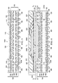
- FIG. 1 illustrates the formation of a workpiece 103 including a substrate 102 , metallization layers and vias 108 on two sides of the substrate 102 , passivation layers 104 and 106 , and redistribution lines (RDLs) 112 and 113 .
- the substrate 102 is made of a semiconductor material such as silicon, germanium, diamond, or the like.
- the substrate 102 is made of compound materials such as silicon germanium, silicon carbide, gallium arsenic, indium arsenide, indium phosphide, silicon germanium carbide, gallium arsenic phosphide, gallium indium phosphide, the like, or a combination thereof.
- the substrate 102 is a silicon-on-insulator (SOI) substrate.
- SOI substrate includes a layer of a semiconductor material such as epitaxial silicon, germanium, silicon germanium, SOI, silicon germanium on insulator (SGOI), or combinations thereof.
- the substrate 102 includes active and passive devices (not shown in FIG. 1 ).
- active and passive devices include active and passive devices (not shown in FIG. 1 ).
- devices such as transistors, capacitors, resistors, combinations of these, and the like may be used for the semiconductor device.
- the devices may be formed using any suitable methods.
- the metallization layers 108 are formed adjacent the active and passive devices and are designed to connect the various devices to form functional circuitry.
- the metallization layers 108 are formed of alternating layers of dielectric (e.g., low-k dielectric material) and conductive material (e.g., copper) with vias interconnecting the layers of conductive material and are formed through any suitable process (such as deposition, damascene, dual damascene, or the like).
- the frontside and backside passivation layers 104 and 106 are formed over and under the substrate 102 as it is oriented in FIG. 1 .
- the passivation layers 104 and 106 can be silicon nitride, silicon carbide, silicon oxide, low-k dielectrics such as carbon doped oxides, extremely low-k dielectrics such as porous carbon doped silicon dioxide, a polymer, such as an epoxy, polyimide, benzocyclobutene (BCB), polybenzoxazole (PBO), the like, or a combination thereof, although other relatively soft, often organic, dielectric materials can also be used.
- the passivation layers 104 and 106 are deposited by chemical vapor deposition (CVD), physical vapor deposition (PVD), atomic layer deposition (ALD), a spin-on-dielectric process, the like, or a combination thereof.
- CVD chemical vapor deposition
- PVD physical vapor deposition
- ALD atomic layer deposition
- spin-on-dielectric process the like, or a combination thereof.
- Redistribution lines (RDLs) 112 and 113 are formed in the passivation layers 104 and 106 , respectively, and are coupled to the metallization layers 108 .
- RDLs 112 and 113 are formed by depositing metal layers, patterning the metal layers, and forming the passivation layers 104 and 106 over the RDLs 112 and 113 , respectively.
- RDLs 112 and 113 are formed using damascene processes.
- the RDLs 112 and 113 are made of a metal or metal alloy including aluminum, copper, tungsten, the like, or a combination thereof.
- FIG. 2 illustrates the formation of connectors 116 on the workpiece 103 (step 502 in FIG. 14 ) and the bonding of a die 120 to the workpiece 103 .
- the connectors 116 are formed on the bond pads 114 and the die 120 is bonded to the workpiece 103 via connectors 118 and bond pads 117 .
- the bond pads 114 and 117 are formed in the passivation layer 104 or on the passivation layer 104 .
- the bond pads 114 and 117 are formed by forming recesses (not shown) into the passivation layer 104 .
- the recesses are formed to allow the bond pads 114 and 117 to be embedded into the passivation layer 104 .
- the recesses are omitted and the bond pads 114 and 117 are formed on the passivation layer 104 .
- the bond pads 114 electrically couple the subsequently bonded connectors 116 to the RDLs 112 and the bond pads 117 electrically couple the subsequently bonded die 120 to the RDLs 117 and/or the connectors 116 .
- the bond pads 114 and 117 include a thin seed layer (not shown) deposited over the workpiece 103 , such as by PVD, CVD, ALD, the like, or a combination thereof.
- the seed layer is made of copper, titanium, nickel, gold, the like, or a combination thereof.
- the conductive material of the bond pads 114 and 117 is deposited over the thin seed layer.
- the conductive material is formed by an electro-chemical plating process, CVD, ALD, PVD, the like, or a combination thereof.
- the conductive material of the bond pads 114 and 117 is copper, tungsten, aluminum, silver, gold, the like, or a combination thereof.
- the bond pads 114 and 117 are UBMs 114 and 117 and include three layers of conductive materials, such as a layer of titanium, a layer of copper, and a layer of nickel.
- conductive materials such as a layer of titanium, a layer of copper, and a layer of nickel.
- suitable arrangements of materials and layers for the formation of the UBMs 114 and 117 are within the contemplated scope of the present disclosure.
- such arrangements include an arrangement of chrome/chrome-copper alloy/copper/gold, an arrangement of titanium/titanium tungsten/copper, an arrangement of copper/nickel/gold, or the like that are suitable.
- any suitable materials or layers of material that may be used for the UBMs 114 and 117 are also within the contemplated scope of the current application.
- the connectors 116 are formed on the bond pads 114 .
- the connectors 116 are subsequently formed into the through-molding vias (TMVs) 130 in FIG. 6 to allow the bottom package 100 in FIG. 6 to be coupled to a top package 200 in FIG. 6 .
- the connectors 116 are illustrated as micro bumps in FIG. 2 .
- the connectors 116 are solder balls, metal pillars, controlled collapse chip connection (C4) bumps, electroless nickel-electroless palladium-immersion gold technique (ENEPIG) formed bumps, or the like.
- the connectors 116 include a conductive material such as solder, copper, aluminum, gold, nickel, silver, palladium, tin, the like, or a combination thereof.
- the connectors 116 are solder bumps
- the connectors 116 are formed by initially forming a layer of solder on the bond pads 114 through various methods such as evaporation, electroplating, printing, solder transfer, ball placement, or the like. In this embodiment, once a layer of solder has been formed on the bond pads 114 , a reflow is performed to shape the material into the desired bump shape.
- the connectors 116 are metal pillars (such as a copper pillars) formed by a sputtering, printing, electro plating, electroless plating, CVD, or the like.
- the metal pillars are solder free and have substantially vertical sidewalls.
- a metal cap layer (not shown) is formed on the top of the metal pillar connectors 116 .
- the metal cap layer includes nickel, tin, tin-lead, gold, silver, palladium, indium, nickel-palladium-gold, nickel-gold, the like, or a combination thereof and is formed by a plating process.
- the die 120 is a device die having integrated circuit devices, such as transistors, capacitors, inductors, resistors (not shown), and the like, therein.
- the die 120 is a logic die having core circuits, and may be, for example, a central processing unit (CPU) die.
- the die 120 includes multiple stacked dies like a memory stacking.
- the connectors 118 are bonded to contacts or bond pads 119 on the die 120 .
- the connectors 118 may be similar to the connectors 116 described above and the description is not repeated herein, although connectors 116 and 118 are not necessarily the same.
- the bonding between the die 120 and the workpiece 103 is a solder bonding or a direct metal-to-metal bonding, such as a copper-to-copper or tin-to-tin bonding.
- the die 120 is bonded to the workpiece 103 by a reflow process. During this reflow process, the connectors 118 are in contact with the bond pads 117 and the die 120 to physically and electrically couple the die 120 to the workpiece 103 .
- molding material 122 is molded on and around the connectors 116 and the die 120 (step 504 in FIG. 14 ).
- the molding material 122 fills the gaps between the connectors 116 and the die 120 , and may be in contact with passivation layer 104 .
- the molding material 122 is filled into the gaps between the die 120 and the passivation layer 104 .
- the molding material 122 is made of a molding compound, a molding underfill, an epoxy, a resin, the like, or a combination thereof.
- the top surface 122 A of the molding material 122 is higher than the top surface 120 A of the die 120 and the top surfaces of the connectors 116 .
- FIG. 4 illustrates the patterning of the molding material 122 to expose the connectors 116 in openings 124 (step 506 in FIG. 14 ).
- a thinning step which may be a grinding step, is performed to thin the molding material 122 , until the top surface 122 A of the molding material 122 is substantially coplanar with the top surface 120 A of the die 120 .
- the molding material 122 undergoes a pressure molding process by a pressure plate or mold (not shown) to shape the molding material 122 and push it into crevices surrounding the die 120 and connectors 116 .
- the molding material is then patterned to form openings 124 in the molding material 122 to expose the connectors 116 .
- the openings 124 are alternatively referred to as TMV openings 124 .
- the TMV openings 124 are formed by a laser ablation or drilling process, an etching process, the like, or a combination thereof.
- the TMV openings 124 have sidewalls 125 which are non-perpendicular and non-parallel to a top surface 103 A of the workpiece 103 with the sidewalls 125 diverging from each other when moving from the bottom surface of the molding material 122 to the top surface 122 A of the molding material 122 .
- a workpiece 103 has TMV openings 124 with a plurality of opening sizes such that the volume of the various TMV openings 124 is different (see FIGS. 9A, 9B, 10A, and 10B ).
- FIG. 5 illustrates the formation of bond pads 126 and connectors 128 on the bottom surface 103 B of the workpiece 103 to allow external devices to be electrically and physically coupled to the bottom package 100 .
- the bond pads 126 and the connectors 128 may be similar to the bond pads 117 and connectors 118 described above and the descriptions are not repeated herein, although the bond pads 117 and 126 or the connectors 118 and 128 are not necessarily the same.
- FIG. 6 illustrates the bonding of a top package 200 to the workpiece 103 (step 508 in FIG. 14 ) of the bottom package 100 to form TMVs 130 .
- the bottom package 100 and the top package 200 has a gap between the two packages.
- the gaps G 1 , G 2 , and G 3 between the packages are substantially equal from edge to edge.
- the gaps G 1 , G 2 , and G 3 vary from edge to edge caused by, for example, warpage of packages, such that a first edge region has a gap G 1 , a middle region has a gap G 2 , and a second edge region has a gap G 3 (see FIGS. 7A, 8A, 11A, 12A, and 13A ).
- the gaps G 1 and G 3 are between the top surface 122 A of the molding material 122 and the bottom surface of the substrate 202 .
- the gap G 2 is between the top surface 120 A of the die 120 and the bottom surface of the substrate 202 .
- the gap G 2 is between the top surface 122 A of the molding material 122 and the bottom surface of the substrate 202 .
- the gap G 1 is from about 0 ⁇ m to about 150 ⁇ m.
- the gap G 2 is from about 0 ⁇ m to about 180 ⁇ m.
- the gap G 3 is from about 0 ⁇ m to about 150 ⁇ m.
- the top package 200 includes a substrate 202 , metallization layers 204 , bond pads 205 and 207 , dies 206 A and 206 B, wire bonds 208 , and molding compound 210 .
- the substrate 202 is made of a semiconductor material such as silicon, germanium, diamond, or the like.
- the substrate 202 is made of compound materials such as silicon germanium, silicon carbide, gallium arsenic, indium arsenide, indium phosphide, silicon germanium carbide, gallium arsenic phosphide, gallium indium phosphide, the like, or a combination thereof.
- the substrate 102 is a silicon-on-insulator (SOI) substrate.
- an SOI substrate includes a layer of a semiconductor material such as epitaxial silicon, germanium, silicon germanium, SOI, silicon germanium on insulator (SGOI), or combinations thereof.
- the substrates 202 are based on an insulating core such as a fiberglass reinforced resin core.
- a fiberglass reinforced resin core such as FR4.
- Alternatives for the core material include bismaleimide-triazine (BT) resin, or alternatively, other PC board materials or films.
- build up films such as Ajinomoto build-up film (ABF) or other laminates are used for substrates 202 .
- the substrate 202 includes active and passive devices (not shown in FIG. 6 ).
- active and passive devices A wide variety of devices such as transistors, capacitors, resistors, combinations of these, and the like may be used for the package 200 .
- the devices may be formed using any suitable methods.
- the top package 200 also includes metallization layers 204 .
- the metallization layers 204 are formed adjacent the active and passive devices and are designed to connect the various devices to form functional circuitry.
- the metallization layers 204 are formed of alternating layers of dielectric (e.g., low-k dielectric material) and conductive material (e.g., copper) with vias interconnecting the layers of conductive material and are formed through any suitable process (such as deposition, damascene, dual damascene, or the like).
- the bond pads 207 electrically couple the dies 206 A and 206 B via the wire bonds 208 to the metallization layers 204 .
- the bond pads 205 electrically couple the TMVs 130 to the metallization layers 204 which allow the bottom package 100 to be electrically coupled to the top package 200 .
- the bond pads 205 and 207 include a thin seed layer (not shown) deposited over the substrate 202 , such as by PVD, CVD, ALD, the like, or a combination thereof.
- the seed layer is made of copper, titanium, nickel, gold, the like, or a combination thereof.
- the conductive material of the bond pads 205 and 207 is deposited over the thin seed layer.
- the conductive material is formed by an electro-chemical plating process, CVD, ALD, PVD, the like, or a combination thereof.
- the conductive material of the bond pads 205 and 207 is copper, tungsten, aluminum, silver, gold, the like, or a combination thereof.
- the bond pads 205 and 207 are UBMs 205 and 207 and include three layers of conductive materials, such as a layer of titanium, a layer of copper, and a layer of nickel.
- conductive materials such as a layer of titanium, a layer of copper, and a layer of nickel.
- chrome/chrome-copper alloy/copper/gold an arrangement of chrome/chrome-copper alloy/copper/gold, an arrangement of titanium/titanium tungsten/copper, or an arrangement of copper/nickel/gold
- Any suitable materials or layers of material that may be used for the UBMs 205 and 207 are within the contemplated scope of the current application.
- the dies 206 A and 206 B are attached to the substrate 202 and coupled to the bond pads 207 by way of wire bonds 208 .
- the dies 206 A and 206 B are device dies having integrated circuit devices, such as transistors, capacitors, inductors, resistors (not shown), and the like, therein.
- the dies 206 A and 206 B are logic dies having core circuits, and may be, for example, a CPU die.
- the dies 206 A and 206 B include multiple stacked dies such as a memory stacking.
- a molding compound 210 is formed over the dies 206 A and 206 B, and wire bonds 208 .
- the molding compound 210 protects the dies 206 A and 206 B and the wire bonds 208 .
- the molding compound 210 is made of a molding compound, a molding underfill, an epoxy, a resin, the like, or a combination thereof.
- the TMVs 130 are bonded to the bond pads 114 and 205 by a reflow process. During this reflow process, the TMVs 130 are in contact with the bond pads 114 and 205 to physically and electrically couple the top package 200 and the bottom package 100 .
- an underfill material (not shown) is injected or otherwise formed in the gap between the bottom package 100 and the top package 200 .
- the underfill material is a liquid epoxy, deformable gel, silicon rubber, or the like, that is dispensed between the bottom package 100 and the top package 200 , and then cured to harden. This underfill material is used, among other things, to reduce cracking in and to protect the TMVs 130 .
- FIG. 7A illustrates a cross-sectional view taken along line A-A of FIG. 7B of a semiconductor device including the bottom package 100 bonded to the top package 200 by a plurality of TMVs 130 .
- FIG. 7B illustrates a top view of FIG. 7A with the top package 200 removed so that the bottom package 100 may be viewed more clearly.
- the gap G 2 in the middle region is smaller than the gaps G 1 and G 3 at the edge regions of the packages 100 and 200 as illustrated in the cross-sectional view of FIG. 7A .
- FIG. 7B illustrates a top view of an embodiment with two sizes 124 A and 124 B of TMV openings 124 .
- FIG. 7B illustrates a semiconductor device with a plurality of regions 300 A having TMV openings 124 A and with a plurality of regions 300 B with TMV openings 124 B.
- the regions 300 A are at the corners of the bottom package 100 , with each of the regions 300 B being between a pair of the regions 300 A and adjacent the die 120 .
- FIG. 7C illustrates a cross-sectional view taken along line B-B of FIG. 7D of a semiconductor device including the bottom package 100 bonded to the top package 200 by a plurality of TMVs 130 .
- FIG. 7D illustrates a top view of FIG. 7C with the top package 200 removed so that the bottom package 100 may be viewed more clearly.
- the gap G 2 in the middle region is smaller than the gaps G 1 and G 3 at the edge regions of the packages 100 and 200 as illustrated in the cross-sectional view of FIG. 7C .
- FIG. 7D illustrates a top view of an embodiment with three sizes 124 A, 124 B, and 124 C of TMV openings 124 with TMV opening 124 C being larger than TMV opening 124 B and TMV opening 124 A being less than opening 124 B.
- This embodiment has a plurality of regions 300 A in the corners of the bottom package 100 , a plurality of regions 300 C having TMV openings 124 C in the centers of each edge of the bottom package 100 , and a plurality of regions 300 B between regions 300 A and 300 C.
- this embodiment is able to handle larger differences between the gap G 2 and gaps G 1 and G 3 .
- FIG. 8A illustrates a cross-sectional view taken along line C-C of FIG. 8B of a semiconductor device including the bottom package 100 bonded to the top package 200 by a plurality of TMVs 130 wherein the gap G 2 is larger than the gaps G 1 and G 3 .
- the bottom package 100 has a plurality of regions 300 A having TMV openings 124 A and a plurality of regions 300 B with TMV openings 124 B.
- the regions 300 B are at the corners of the bottom package 100 , with each of the regions 300 A between a pair of the regions 300 B and adjacent the die 120 .
- FIGS. 9A and 9B illustrate TMV openings 124 A 1 and 124 B 1 , respectively, of different sizes.
- the TMV openings 124 A 1 and 124 B 1 extend through the molding material 122 to the top surface 103 A of the workpiece 103 .
- the TMV opening 124 A 1 has a width W A1 at the top surface 122 A of the molding material 122 and a width W A2 at the bottom surface of the molding material 122 with W A2 being less than W A1 .
- the TMV opening 124 B 1 has a width W B1 at the top surface 122 A of the molding material 122 and a width W B2 at the bottom surface of the molding material 122 with W B2 being less than W B1 and greater than W A2 .
- the TMV opening 124 B 1 has a larger volume than the TMV opening 124 A 1 .
- the widths W A1 , W A2 , W B1 , and W B2 are from 30 ⁇ m to about 1000 ⁇ m.
- the various widths of the TMV openings 124 A 1 and 124 B 1 are controlled by, for example, the laser ablation process that patterns the molding material 122 .
- FIGS. 10A and 10B illustrate TMV openings 124 A 2 and 124 B 2 which are similar to TMV openings 124 A 1 and 124 B 1 , respectively, except that some molding material 122 is left on the top surface 103 A of the workpiece 103 in the TMV openings 124 A 2 and 124 B 2 .
- the TMV opening 124 A 2 has a depth D A1 which is less than the thickness of the molding material 122 ; hence the opening 124 A 2 does not extend all the way through the molding material 122 .
- the TMV opening 124 B 2 has a depth D B1 which is less than the thickness of the molding material 122 ; hence the opening 124 B 2 does not extend all the way through the molding material 122 .
- a single semiconductor device includes TMV openings 124 of more than one size such that a semiconductor device includes some TMV openings 124 A ( 124 A 1 and/or 124 A 2 ) and some TMV openings 124 B ( 124 B 1 and/or 124 B 2 ).
- the difference between the widths W B2 and W A2 is greater than 20 ⁇ m.
- FIG. 11A illustrates a cross-sectional view taken along line D-D of FIG. 11B of a semiconductor device including the bottom package 100 bonded to the top package 200 by a plurality of TMVs 130 wherein the gap G 2 is larger than the gaps G 1 and G 3 and also including a gap G 4 on either side of the gap G 2 with the gap G 4 being smaller than gaps G 1 and G 3 .
- the bottom package 100 has a plurality of regions 300 A having TMV openings 124 A and with a plurality of regions 300 B with TMV openings 124 B.
- a first set of the regions 300 A are at the corners of the bottom package 100
- a second set of the regions 300 A are in the centers of each edge of the bottom package 100
- each of the regions 300 B being between a pair of regions 300 A.
- FIG. 12A illustrates a cross-sectional view taken along line E-E of FIG. 12B of a semiconductor device including the bottom package 100 bonded to the top package 200 by a plurality of TMVs 130 wherein the gap G 3 is larger than the gap G 2 which is larger than the gap G 1 .
- the bottom package 100 has a region 300 A having TMV openings 124 A, a region 300 C with TMV openings 124 C, and a region 300 B with TMV openings 124 B, the region 300 B being between the regions 300 A and 300 C.
- the regions 300 A, 300 B, and 300 C are rectangular with region 300 C aligned along an edge of the bottom package 100 and region 300 A aligned along an opposite edge of the bottom package 100 with region 300 B between regions 300 C and 300 A.
- FIG. 12C illustrates a cross-sectional view taken along line F-F of FIG. 12D of a semiconductor device including the bottom package 100 bonded to the top package 200 by a plurality of TMVs 130 wherein the gap G 3 is larger than the gap G 2 which is larger than the gap G 1 .
- the bottom package 100 has a region 300 A having TMV openings 124 A, a region 300 C with TMV openings 124 C, and a region 300 B with TMV openings 124 B, the region 300 B being between the regions 300 A and 300 C.
- the regions 300 A and 300 C are triangular with a corner of the triangle being aligned with a corner of the bottom package 100
- region 300 B is between the regions 300 A and 300 C.
- FIG. 13A illustrates a cross-sectional view taken along line G-G of FIG. 13B of a semiconductor device including the bottom package 100 bonded to the top package 200 by a plurality of TMVs 130 wherein the gap G 2 is larger than the gap G 1 and the gap G 3 is larger than the gap G 2 with a gap G 5 laterally between gaps G 2 and G 3 and gap G 5 being smaller than gap G 1 .
- the bottom package 100 has at least one region 300 B having TMV openings 124 B and at least one region 300 A with TMV openings 124 A. Further, the at least one region 300 B is aligned with the gap G 5 and the at least one regions 300 A is covering the remaining area of the bottom package 100 .
- the warpage of the top and bottom packages 200 and 100 varies greatly between designs and thus affects the process yield.
- the warpage of the packages can be measured during prototyping such that the TMV opening sizes 124 A, 124 B, and 124 C in the various regions 300 A, 300 B, and 300 C are configured to improve the process yield.
- the process yield is increased because the possibility of a bridge between adjacent TMVs is reduced.
- TMV openings 124 A are smaller in the regions (e.g., regions 300 A) where the gaps are larger (see e.g., FIGS. 7A-7D and 8A-8B ).
- the process yield is increased because the possibility of a cold joint for a TMV 130 is reduced.
- An embodiment is a semiconductor device including a molding material over a first substrate with a first opening having a first width in the molding material.
- the semiconductor device further includes a second opening having a second width in the molding material with the second width being greater than the first width.
- a first connector is in the first opening and a second connector is in the second opening.
- Another embodiment is a package including a bottom package and a top package including at least one active device.
- the bottom package includes a first die over a first substrate and a molding material over the first substrate surrounding the first die.
- the bottom package further includes a plurality of openings in the molding material with at least one of the plurality of openings having a first width at a first surface of the at least one opening, and at least one other of the plurality of openings having a second width at a first surface of the at least one other opening, the second width being greater than the first width.
- the bottom package further includes a plurality of through-molding vias (TMVs) over the first substrate, each of the plurality of TMVs being in one of the plurality of openings.
- the top package being couple to the plurality of TMVs.
- a further embodiment is a method of forming a semiconductor device including forming a molding material over a first substrate and forming a first opening in the molding material with the first opening having a first width.
- the method further includes forming a second opening in the molding material with the second opening having a second width.
- the second width is larger than the first width.
- the method further includes forming a first through-molding via (TMV) in the first opening and a second TMV in the second opening.
- TMV through-molding via
Landscapes
- Internal Circuitry In Semiconductor Integrated Circuit Devices (AREA)
- Engineering & Computer Science (AREA)
- Physics & Mathematics (AREA)
- Geometry (AREA)
- Manufacturing & Machinery (AREA)
- Microelectronics & Electronic Packaging (AREA)
- Structures Or Materials For Encapsulating Or Coating Semiconductor Devices Or Solid State Devices (AREA)
Abstract
Embodiments of the present disclosure include a semiconductor device, a package and methods of forming a semiconductor device and a package. An embodiment is a semiconductor device including a molding material over a first substrate with a first opening having a first width in the molding material. The semiconductor device further includes a second opening having a second width in the molding material with the second width being greater than the first width. A first connector is in the first opening and a second connector is in the second opening.
Description
This application claims the benefit to and is a divisional of U.S. patent application Ser. No. 13/961,589, filed on Aug. 7, 2013, and entitled “3D Packages and Methods for Forming the Same” which application is incorporated herein by reference.
Since the invention of the integrated circuit (IC), the semiconductor industry has experienced rapid growth due to continuous improvements in the integration density of various electronic components (i.e., transistors, diodes, resistors, capacitors, etc.). For the most part, this improvement in integration density has come from repeated reductions in minimum feature size, which allows more components to be integrated into a given area.
These integration improvements are essentially two-dimensional (2D) in nature, in that the volume occupied by the integrated components is essentially on the surface of the semiconductor wafer. Although dramatic improvement in lithography has resulted in considerable improvement in 2D IC formation, there are physical limits to the density that can be achieved in two dimensions. One of these limits is the minimum size needed to make these components. In addition, when more devices are put into one chip or die, more complex designs are required.
For a more complete understanding of the present embodiments, and the advantages thereof, reference is now made to the following descriptions taken in conjunction with the accompanying drawings, in which:
Reference will now be made in detail to embodiments illustrated in the accompanying drawings. Wherever possible, the same reference numbers are used in the drawings and the description to refer to the same or like parts. In the drawings, the shape and thickness may be exaggerated for clarity and convenience. This description will be directed in particular to elements forming part of, or cooperating more directly with, methods and apparatus in accordance with the present disclosure. It is to be understood that elements not specifically shown or described may take various forms well known to those skilled in the art. Many alternatives and modifications will be apparent to those skilled in the art, once informed by the present disclosure.
Reference throughout this specification to “one embodiment” or “an embodiment” means that a particular feature, structure, or characteristic described in connection with the embodiment is included in at least one embodiment. Thus, the appearances of the phrases “in one embodiment” or “in an embodiment” in various places throughout this specification are not necessarily all referring to the same embodiment. Furthermore, the particular features, structures, or characteristics may be combined in any suitable manner in one or more embodiments. It should be appreciated that the following figures are not drawn to scale; rather, these figures are merely intended for illustration.
Embodiments will be described with respect to a specific context, namely a semiconductor device including more than one through molding via configuration. Other embodiments may also be applied, however, to other package structure configurations.
In some embodiments, the substrate 102 includes active and passive devices (not shown in FIG. 1 ). As one of ordinary skill in the art will recognize, a wide variety of devices such as transistors, capacitors, resistors, combinations of these, and the like may be used for the semiconductor device. The devices may be formed using any suitable methods.
There are metallization layers 108 on two sides the substrate 102. The metallization layers 108 are formed adjacent the active and passive devices and are designed to connect the various devices to form functional circuitry. The metallization layers 108 are formed of alternating layers of dielectric (e.g., low-k dielectric material) and conductive material (e.g., copper) with vias interconnecting the layers of conductive material and are formed through any suitable process (such as deposition, damascene, dual damascene, or the like).
The frontside and backside passivation layers 104 and 106, respectively, are formed over and under the substrate 102 as it is oriented in FIG. 1 . The passivation layers 104 and 106 can be silicon nitride, silicon carbide, silicon oxide, low-k dielectrics such as carbon doped oxides, extremely low-k dielectrics such as porous carbon doped silicon dioxide, a polymer, such as an epoxy, polyimide, benzocyclobutene (BCB), polybenzoxazole (PBO), the like, or a combination thereof, although other relatively soft, often organic, dielectric materials can also be used. In some embodiments, the passivation layers 104 and 106 are deposited by chemical vapor deposition (CVD), physical vapor deposition (PVD), atomic layer deposition (ALD), a spin-on-dielectric process, the like, or a combination thereof.
Redistribution lines (RDLs) 112 and 113 are formed in the passivation layers 104 and 106, respectively, and are coupled to the metallization layers 108. In some embodiments, RDLs 112 and 113 are formed by depositing metal layers, patterning the metal layers, and forming the passivation layers 104 and 106 over the RDLs 112 and 113, respectively. In alternative embodiments, RDLs 112 and 113 are formed using damascene processes. In some embodiments, the RDLs 112 and 113 are made of a metal or metal alloy including aluminum, copper, tungsten, the like, or a combination thereof.
In an embodiment, the bond pads 114 and 117 are UBMs 114 and 117 and include three layers of conductive materials, such as a layer of titanium, a layer of copper, and a layer of nickel. However, many suitable arrangements of materials and layers for the formation of the UBMs 114 and 117 are within the contemplated scope of the present disclosure. For example, such arrangements include an arrangement of chrome/chrome-copper alloy/copper/gold, an arrangement of titanium/titanium tungsten/copper, an arrangement of copper/nickel/gold, or the like that are suitable. Further, any suitable materials or layers of material that may be used for the UBMs 114 and 117 are also within the contemplated scope of the current application.
After the bond pads 114 are formed, the connectors 116 are formed on the bond pads 114. The connectors 116 are subsequently formed into the through-molding vias (TMVs) 130 in FIG. 6 to allow the bottom package 100 in FIG. 6 to be coupled to a top package 200 in FIG. 6 . The connectors 116 are illustrated as micro bumps in FIG. 2 . However, in other embodiments, the connectors 116 are solder balls, metal pillars, controlled collapse chip connection (C4) bumps, electroless nickel-electroless palladium-immersion gold technique (ENEPIG) formed bumps, or the like. The connectors 116 include a conductive material such as solder, copper, aluminum, gold, nickel, silver, palladium, tin, the like, or a combination thereof. In an embodiment in which the connectors 116 are solder bumps, the connectors 116 are formed by initially forming a layer of solder on the bond pads 114 through various methods such as evaporation, electroplating, printing, solder transfer, ball placement, or the like. In this embodiment, once a layer of solder has been formed on the bond pads 114, a reflow is performed to shape the material into the desired bump shape. In another embodiment, the connectors 116 are metal pillars (such as a copper pillars) formed by a sputtering, printing, electro plating, electroless plating, CVD, or the like. In an embodiment, the metal pillars are solder free and have substantially vertical sidewalls. In some embodiments, a metal cap layer (not shown) is formed on the top of the metal pillar connectors 116. In some embodiments, the metal cap layer includes nickel, tin, tin-lead, gold, silver, palladium, indium, nickel-palladium-gold, nickel-gold, the like, or a combination thereof and is formed by a plating process.
After the bond pads 117 are formed, an active surface of the dies 120 that has the connectors 118 is bonded to the top surface 103A of the workpiece 103 by way of the connectors 118 and the bond pads 117. In an embodiment, the die 120 is a device die having integrated circuit devices, such as transistors, capacitors, inductors, resistors (not shown), and the like, therein. In another embodiment, the die 120 is a logic die having core circuits, and may be, for example, a central processing unit (CPU) die. In some embodiments, the die 120 includes multiple stacked dies like a memory stacking. The connectors 118 are bonded to contacts or bond pads 119 on the die 120. The connectors 118 may be similar to the connectors 116 described above and the description is not repeated herein, although connectors 116 and 118 are not necessarily the same.
In some embodiments, the bonding between the die 120 and the workpiece 103 is a solder bonding or a direct metal-to-metal bonding, such as a copper-to-copper or tin-to-tin bonding. In an embodiment, the die 120 is bonded to the workpiece 103 by a reflow process. During this reflow process, the connectors 118 are in contact with the bond pads 117 and the die 120 to physically and electrically couple the die 120 to the workpiece 103.
After the connectors 116 are formed and the die 120 is placed, molding material 122 is molded on and around the connectors 116 and the die 120 (step 504 in FIG. 14 ). The molding material 122 fills the gaps between the connectors 116 and the die 120, and may be in contact with passivation layer 104. In an embodiment, the molding material 122 is filled into the gaps between the die 120 and the passivation layer 104. In some embodiments, the molding material 122 is made of a molding compound, a molding underfill, an epoxy, a resin, the like, or a combination thereof. In some embodiments, the top surface 122A of the molding material 122 is higher than the top surface 120A of the die 120 and the top surfaces of the connectors 116.
The top package 200 includes a substrate 202, metallization layers 204, bond pads 205 and 207, dies 206A and 206B, wire bonds 208, and molding compound 210. In some embodiments, the substrate 202 is made of a semiconductor material such as silicon, germanium, diamond, or the like. In other embodiments, the substrate 202 is made of compound materials such as silicon germanium, silicon carbide, gallium arsenic, indium arsenide, indium phosphide, silicon germanium carbide, gallium arsenic phosphide, gallium indium phosphide, the like, or a combination thereof. In an embodiment, the substrate 102 is a silicon-on-insulator (SOI) substrate. Generally, an SOI substrate includes a layer of a semiconductor material such as epitaxial silicon, germanium, silicon germanium, SOI, silicon germanium on insulator (SGOI), or combinations thereof. In some embodiments, the substrates 202 are based on an insulating core such as a fiberglass reinforced resin core. One example of the core material is fiberglass resin such as FR4. Alternatives for the core material include bismaleimide-triazine (BT) resin, or alternatively, other PC board materials or films. In some embodiments, build up films such as Ajinomoto build-up film (ABF) or other laminates are used for substrates 202.
In some embodiments, the substrate 202 includes active and passive devices (not shown in FIG. 6 ). A wide variety of devices such as transistors, capacitors, resistors, combinations of these, and the like may be used for the package 200. The devices may be formed using any suitable methods.
The top package 200 also includes metallization layers 204. The metallization layers 204 are formed adjacent the active and passive devices and are designed to connect the various devices to form functional circuitry. The metallization layers 204 are formed of alternating layers of dielectric (e.g., low-k dielectric material) and conductive material (e.g., copper) with vias interconnecting the layers of conductive material and are formed through any suitable process (such as deposition, damascene, dual damascene, or the like).
The bond pads 207 electrically couple the dies 206A and 206B via the wire bonds 208 to the metallization layers 204. The bond pads 205 electrically couple the TMVs 130 to the metallization layers 204 which allow the bottom package 100 to be electrically coupled to the top package 200. In some embodiments, the bond pads 205 and 207 include a thin seed layer (not shown) deposited over the substrate 202, such as by PVD, CVD, ALD, the like, or a combination thereof. The seed layer is made of copper, titanium, nickel, gold, the like, or a combination thereof. The conductive material of the bond pads 205 and 207 is deposited over the thin seed layer. In some embodiments, the conductive material is formed by an electro-chemical plating process, CVD, ALD, PVD, the like, or a combination thereof. In an embodiment, the conductive material of the bond pads 205 and 207 is copper, tungsten, aluminum, silver, gold, the like, or a combination thereof.
In an embodiment the bond pads 205 and 207 are UBMs 205 and 207 and include three layers of conductive materials, such as a layer of titanium, a layer of copper, and a layer of nickel. However, many suitable arrangements of materials and layers, such as an arrangement of chrome/chrome-copper alloy/copper/gold, an arrangement of titanium/titanium tungsten/copper, or an arrangement of copper/nickel/gold, are suitable for the formation of the UBMs 205 and 207. Any suitable materials or layers of material that may be used for the UBMs 205 and 207 are within the contemplated scope of the current application.
After the bond pads 207 are formed, the dies 206A and 206B are attached to the substrate 202 and coupled to the bond pads 207 by way of wire bonds 208. In some embodiments, the dies 206A and 206B are device dies having integrated circuit devices, such as transistors, capacitors, inductors, resistors (not shown), and the like, therein. In other embodiments, the dies 206A and 206B are logic dies having core circuits, and may be, for example, a CPU die. In some embodiments, the dies 206A and 206B include multiple stacked dies such as a memory stacking.
In an embodiment, a molding compound 210 is formed over the dies 206A and 206B, and wire bonds 208. The molding compound 210 protects the dies 206A and 206B and the wire bonds 208. In some embodiments, the molding compound 210 is made of a molding compound, a molding underfill, an epoxy, a resin, the like, or a combination thereof.
In some embodiments, the bonding between the top package 200 and the bottom package 100—by way of bond pads 205, TMVs 130, and bond pads 114—is a solder bonding or a direct metal-to-metal bonding, such as a copper-to-copper or tin-to-tin bonding. In an embodiment, the TMVs 130 are bonded to the bond pads 114 and 205 by a reflow process. During this reflow process, the TMVs 130 are in contact with the bond pads 114 and 205 to physically and electrically couple the top package 200 and the bottom package 100.
In an embodiment, an underfill material (not shown) is injected or otherwise formed in the gap between the bottom package 100 and the top package 200. In some embodiments, the underfill material is a liquid epoxy, deformable gel, silicon rubber, or the like, that is dispensed between the bottom package 100 and the top package 200, and then cured to harden. This underfill material is used, among other things, to reduce cracking in and to protect the TMVs 130.
In some embodiments, a single semiconductor device includes TMV openings 124 of more than one size such that a semiconductor device includes some TMV openings 124A (124A1 and/or 124A2) and some TMV openings 124B (124B1 and/or 124B2). In some embodiments, the difference between the widths WB2 and WA2 is greater than 20 μm.
The warpage of the top and bottom packages 200 and 100, respectively, varies greatly between designs and thus affects the process yield. The warpage of the packages can be measured during prototyping such that the TMV opening sizes 124A, 124B, and 124C in the various regions 300A, 300B, and 300C are configured to improve the process yield. By having the larger TMV openings 124 (e.g., TMV openings 124B and/or 124C) in the regions (e.g., 300B and 300C) where the gaps are smaller (see e.g., FIGS. 7A-7D and 8A-8B ), the process yield is increased because the possibility of a bridge between adjacent TMVs is reduced. Also, by having smaller TMV openings (e.g., TMV openings 124A) in the regions (e.g., regions 300A) where the gaps are larger (see e.g., FIGS. 7A-7D and 8A-8B ), the process yield is increased because the possibility of a cold joint for a TMV 130 is reduced.
An embodiment is a semiconductor device including a molding material over a first substrate with a first opening having a first width in the molding material. The semiconductor device further includes a second opening having a second width in the molding material with the second width being greater than the first width. A first connector is in the first opening and a second connector is in the second opening.
Another embodiment is a package including a bottom package and a top package including at least one active device. The bottom package includes a first die over a first substrate and a molding material over the first substrate surrounding the first die. The bottom package further includes a plurality of openings in the molding material with at least one of the plurality of openings having a first width at a first surface of the at least one opening, and at least one other of the plurality of openings having a second width at a first surface of the at least one other opening, the second width being greater than the first width. The bottom package further includes a plurality of through-molding vias (TMVs) over the first substrate, each of the plurality of TMVs being in one of the plurality of openings. The top package being couple to the plurality of TMVs.
A further embodiment is a method of forming a semiconductor device including forming a molding material over a first substrate and forming a first opening in the molding material with the first opening having a first width. The method further includes forming a second opening in the molding material with the second opening having a second width. The second width is larger than the first width. The method further includes forming a first through-molding via (TMV) in the first opening and a second TMV in the second opening.
Although the present embodiments and their advantages have been described in detail, it should be understood that various changes, substitutions, and alterations can be made herein without departing from the spirit and scope of the disclosure as defined by the appended claims. Moreover, the scope of the present application is not intended to be limited to the particular embodiments of the process, machine, manufacture, composition of matter, means, methods, and operations described in the specification. As one of ordinary skill in the art will readily appreciate from the disclosure, processes, machines, manufacture, compositions of matter, means, methods, or operations, presently existing or later to be developed, that perform substantially the same function or achieve substantially the same result as the corresponding embodiments described herein may be utilized according to the present disclosure. Accordingly, the appended claims are intended to include within their scope such processes, machines, manufacture, compositions of matter, means, methods, or operations.
Claims (20)
1. A method of forming a semiconductor device, the method comprising:
molding a molding material over a first substrate, the first substrate comprising a first edge region, a middle region next to the first edge region, and a second edge region next to the middle region and opposite the first edge region;
forming a first opening in the molding material in the first edge region, the first opening having a first width;
forming a first connector in the first opening;
forming a second opening in the molding material in the middle region, the second opening having a second width, the second width being greater than the first width;
forming a second connector in the second opening;
forming a third opening in the in the molding material in the second edge region, the third opening having a third width, the third width being greater than the second width;
forming a third connector in the third opening; and
bonding a second package to the first connector, the second connector, and the third connector, a first surface of the second package being physically separated from a first surface of the molding material by a first gap in the first edge region, a second gap in the middle region, and a third gap in the second edge region, the first gap being greater than the second gap, and the second gap being greater than the third gap.
2. The method of claim 1 , wherein the forming the first opening in the molding material comprises a laser ablation process.
3. The method of claim 1 , wherein at least one of the first and second connectors are through-molding vias (TMVs).
4. The method of claim 1 , wherein sidewalls of at least one of the first, second, and third openings are non-perpendicular and non-parallel to a first surface of the first substrate.
5. The method of claim 1 , further comprising forming a die over the first substrate, a first surface of the molding material being coplanar with a first surface of the die.
6. The method of claim 1 , wherein the first substrate comprises a first plurality of metallization layers and vias on a first side of the first substrate and a second plurality of metallization layers and vias on a second side of the first substrate, the first side being opposite the second side.
7. The method of claim 1 , wherein forming the first opening, forming the second opening, and forming the third opening comprises drilling the first opening, the second opening, and the third opening to a depth that is less than a thickness of the molding material.
8. The method of claim 1 , wherein in a top down view, the first edge region, the middle region, and the second edge region are rectangular, and wherein the second edge region is wider than the middle region, and the middle region is wider than the first edge region.
9. A method of forming a semiconductor device, the method comprising:
forming a first plurality of metallization layers and vias on a first side of a substrate;
forming a second plurality of metallization layers and vias on a second side of the substrate, the second side being opposite the first side;
bonding a die on the first side of the substrate;
forming a first plurality of connectors on the first side of the substrate;
molding a molding material on the first side of the substrate, a top surface of the molding material being coplanar with a top surface of the die, and the molding material having a first region, a second region, and a third region;
forming a plurality of first openings in the molding material in the first region and the third region, the plurality of first openings having a first width at the top surface of the molding material;
forming a plurality of second openings in the molding material in the second region, the plurality of second openings having a second width at the top surface of the molding material, the second width being greater than the first width; and
forming a plurality of through-molding vias (TMVs) over the substrate, each of the plurality of TMVs being in one of the first plurality of openings or the second plurality of openings.
10. The method of claim 9 , further comprising coupling a top package to the plurality of TMVs.
11. The method of claim 10 , wherein coupling the top package to the plurality of TMVs further comprises:
creating a first gap between the top surface of the molding material and a first surface of the top package in the first region; and
creating a second gap between the top surface of the molding material and the first surface of the top package in the second region, the first gap being larger than the second gap.
12. The method of claim 11 , wherein coupling the top package to the plurality of TMVs further comprises creating a third gap between the top surface of the molding material and the first surface of the top package in the third region, the third gap being larger than the second gap and smaller than the first gap.
13. The method of claim 9 , wherein the third region is in each corner of the substrate, the first region is in the center of each edge of the substrate, and the second region is laterally between each of the first and third regions along each edge of the substrate.
14. The method of claim 9 , wherein molding the molding material comprises:
pressure molding the molding material to shape the molding material and press it into crevices surrounding the die and the first plurality of connectors; and
thinning the molding material until the top surface of the molding material is coplanar with the top surface of the die.
15. The method of claim 9 , wherein bonding the die on the first side of the substrate further comprises bonding the die to a second plurality of connectors formed on the first side of the substrate.
16. The method of claim 9 , further comprising forming a second plurality of connectors on the second side of the substrate, the second plurality of connectors being configured to couple external devices to the substrate.
17. A method of forming a package, the method comprising:
forming a bottom package having a first region, a second region, and a third region, the first and third regions being triangular from a top down view, a corner of each triangle being aligned with a respective diagonally opposite corner of the bottom package, wherein forming the bottom package further comprises:
forming a molding material over a first substrate;
forming a first plurality of openings in the molding material in the first region, the first plurality of openings having a first width at a first surface of the molding material;
forming a second plurality of openings in the molding material in the second region, the second plurality of openings having a second width at the first surface of the molding material, the second width being greater than the first width;
forming a third plurality of openings in the molding material in the third region, the third plurality of openings having a third width at the first surface of the molding material, the third width being greater than the second width; and
forming a plurality of through-molding vias (TMVs) over the first substrate, each of the plurality of TMVs being in one of the first, second, and third plurality of openings; and
coupling a top package to the plurality of TMVs, the top package comprising at least one active device, the first region having a first gap between the first surface of the molding material and a first surface of the top package, the second region having a second gap between the first surface of the molding material and the first surface of the top package, the second gap being smaller than the first gap, and the third region having a third gap between the first surface of the molding material and the first surface of the top package, the third gap being smaller than the second gap.
18. The method of claim 17 , wherein sidewalls of the first and second plurality of openings are non-perpendicular and non-parallel to a major surface of the first substrate.
19. The method of claim 17 , further comprising placing a die over the first substrate in the bottom package, the first surface of the molding material being coplanar with a first surface of the die.
20. The method of claim 17 , wherein forming the first plurality of openings, forming the second plurality of openings, and forming the third plurality of openings comprises etching the first plurality of openings, the second plurality of openings, and the third plurality of openings to a depth less than a thickness of the molding material.
Priority Applications (1)
| Application Number | Priority Date | Filing Date | Title |
|---|---|---|---|
| US14/970,250 US9543284B2 (en) | 2013-08-07 | 2015-12-15 | 3D packages and methods for forming the same |
Applications Claiming Priority (2)
| Application Number | Priority Date | Filing Date | Title |
|---|---|---|---|
| US13/961,589 US9252076B2 (en) | 2013-08-07 | 2013-08-07 | 3D packages and methods for forming the same |
| US14/970,250 US9543284B2 (en) | 2013-08-07 | 2015-12-15 | 3D packages and methods for forming the same |
Related Parent Applications (1)
| Application Number | Title | Priority Date | Filing Date |
|---|---|---|---|
| US13/961,589 Division US9252076B2 (en) | 2013-08-07 | 2013-08-07 | 3D packages and methods for forming the same |
Publications (2)
| Publication Number | Publication Date |
|---|---|
| US20160111409A1 US20160111409A1 (en) | 2016-04-21 |
| US9543284B2 true US9543284B2 (en) | 2017-01-10 |
Family
ID=52447955
Family Applications (2)
| Application Number | Title | Priority Date | Filing Date |
|---|---|---|---|
| US13/961,589 Active 2033-10-13 US9252076B2 (en) | 2013-08-07 | 2013-08-07 | 3D packages and methods for forming the same |
| US14/970,250 Active US9543284B2 (en) | 2013-08-07 | 2015-12-15 | 3D packages and methods for forming the same |
Family Applications Before (1)
| Application Number | Title | Priority Date | Filing Date |
|---|---|---|---|
| US13/961,589 Active 2033-10-13 US9252076B2 (en) | 2013-08-07 | 2013-08-07 | 3D packages and methods for forming the same |
Country Status (2)
| Country | Link |
|---|---|
| US (2) | US9252076B2 (en) |
| KR (1) | KR101620702B1 (en) |
Cited By (2)
| Publication number | Priority date | Publication date | Assignee | Title |
|---|---|---|---|---|
| US20190229483A1 (en) * | 2018-01-25 | 2019-07-25 | Lotes Co., Ltd | Electrical connector retaining device |
| US12563672B2 (en) * | 2020-12-31 | 2026-02-24 | Huawei Technologies Co., Ltd. | Board-level structure and communication device |
Families Citing this family (26)
| Publication number | Priority date | Publication date | Assignee | Title |
|---|---|---|---|---|
| KR20150096949A (en) * | 2014-02-17 | 2015-08-26 | 삼성전자주식회사 | A semiconductor package and method of forming the same |
| US9064718B1 (en) * | 2014-05-07 | 2015-06-23 | Freescale Semiconductor, Inc. | Pre-formed via array for integrated circuit package |
| KR20150144416A (en) * | 2014-06-16 | 2015-12-28 | 한국전자통신연구원 | Stack module package and method for manufacturing of the same |
| US9666559B2 (en) | 2014-09-05 | 2017-05-30 | Invensas Corporation | Multichip modules and methods of fabrication |
| TWI560827B (en) * | 2014-09-15 | 2016-12-01 | Siliconware Precision Industries Co Ltd | Semiconductor package and its carrier structure and method of manufacture |
| US10325853B2 (en) * | 2014-12-03 | 2019-06-18 | Taiwan Semiconductor Manufacturing Company, Ltd. | Method of forming semiconductor packages having through package vias |
| US10032704B2 (en) | 2015-02-13 | 2018-07-24 | Taiwan Semiconductor Manufacturing Company, Ltd. | Reducing cracking by adjusting opening size in pop packages |
| TWI595810B (en) * | 2015-05-22 | 2017-08-11 | 欣興電子股份有限公司 | Package structure and manufacturing method thereof |
| CN106298707B (en) * | 2015-06-05 | 2019-05-21 | 欣兴电子股份有限公司 | Package structure and method of making the same |
| US10483211B2 (en) * | 2016-02-22 | 2019-11-19 | Mediatek Inc. | Fan-out package structure and method for forming the same |
| US9659911B1 (en) * | 2016-04-20 | 2017-05-23 | Powertech Technology Inc. | Package structure and manufacturing method thereof |
| US12550783B2 (en) | 2016-05-17 | 2026-02-10 | Taiwan Semiconductor Manufacturing Company, Ltd. | Device and method for UBM/RDL routing |
| CN107579061B (en) | 2016-07-04 | 2020-01-07 | 晟碟信息科技(上海)有限公司 | Semiconductor device including interconnected stacked package |
| US20180053753A1 (en) * | 2016-08-16 | 2018-02-22 | Freescale Semiconductor, Inc. | Stackable molded packages and methods of manufacture thereof |
| US9768133B1 (en) * | 2016-09-22 | 2017-09-19 | Taiwan Semiconductor Manufacturing Company, Ltd. | Semiconductor package and method of forming the same |
| US20180180808A1 (en) * | 2016-12-22 | 2018-06-28 | Oracle International Corporation | Wafer-level packaged optoelectronic module |
| US10319683B2 (en) | 2017-02-08 | 2019-06-11 | Taiwan Semiconductor Manufacturing Company, Ltd. | Multi-stacked package-on-package structures |
| CN108695284A (en) * | 2017-04-07 | 2018-10-23 | 晟碟信息科技(上海)有限公司 | Include the semiconductor equipment of Top-down design semiconductor package body group |
| CN110770031A (en) * | 2017-07-26 | 2020-02-07 | 惠普发展公司,有限责任合伙企业 | Die Contact Structure |
| US10867929B2 (en) | 2018-12-05 | 2020-12-15 | Taiwan Semiconductor Manufacturing Company, Ltd. | Semiconductor structures and methods of forming the same |
| US20200312733A1 (en) * | 2019-03-29 | 2020-10-01 | Advanced Semiconductor Engineering, Inc. | Semiconductor package structure and method for manufacturing the same |
| US11664300B2 (en) * | 2019-12-26 | 2023-05-30 | Taiwan Semiconductor Manufacturing Co., Ltd. | Fan-out packages and methods of forming the same |
| CN113990759B (en) * | 2020-12-21 | 2025-07-22 | 矽磐微电子(重庆)有限公司 | Semiconductor packaging method and semiconductor packaging structure |
| US11961808B2 (en) * | 2021-10-14 | 2024-04-16 | Advanced Semiconductor Engineering, Inc. | Electronic package structure with reinforcement element |
| US12183683B2 (en) * | 2021-10-14 | 2024-12-31 | Advanced Semiconductor Engineering, Inc. | Electronic package structure |
| US20230361014A1 (en) * | 2022-05-06 | 2023-11-09 | Advanced Semiconductor Engineering, Inc. | Electronic package |
Citations (35)
| Publication number | Priority date | Publication date | Assignee | Title |
|---|---|---|---|---|
| US6222272B1 (en) | 1996-08-06 | 2001-04-24 | Nitto Denko Corporation | Film carrier and semiconductor device using same |
| US6392143B1 (en) * | 1999-01-18 | 2002-05-21 | Kabushiki Kaisha Toshiba | Flexible package having very thin semiconductor chip, module and multi chip module (MCM) assembled by the package, and method for manufacturing the same |
| US20040207052A1 (en) | 2002-08-30 | 2004-10-21 | Rajeev Joshi | Substrate based unmolded package |
| US20070152350A1 (en) * | 2006-01-04 | 2007-07-05 | Samsung Electronics Co., Ltd. | Wiring substrate having variously sized ball pads, semiconductor package having the wiring substrate, and stack package using the semiconductor package |
| KR20080061969A (en) | 2006-12-28 | 2008-07-03 | 주식회사 하이닉스반도체 | Semiconductor package and manufacturing method thereof |
| US20080157353A1 (en) | 2006-12-29 | 2008-07-03 | Texas Instruments Incorporated | Control of Standoff Height Between Packages with a Solder-Embedded Tape |
| US20090039490A1 (en) * | 2007-08-08 | 2009-02-12 | Powertech Technology Inc. | Mounting assembly of semiconductor packages prevent soldering defects caused by substrate warpage |
| JP2009099669A (en) | 2007-10-15 | 2009-05-07 | Nec Corp | Electronic component mounting structure and mounting method |
| JP2009105441A (en) | 2009-02-04 | 2009-05-14 | Nec Infrontia Corp | Semiconductor device |
| US20100072600A1 (en) | 2008-09-22 | 2010-03-25 | Texas Instrument Incorporated | Fine-pitch oblong solder connections for stacking multi-chip packages |
| US20100283140A1 (en) | 2009-05-08 | 2010-11-11 | Samsung Electronics Co., Ltd. | Package on package to prevent circuit pattern lift defect and method of fabricating the same |
| US20110037156A1 (en) * | 2009-08-13 | 2011-02-17 | Qualcomm Incorporated | Variable Feature Interface That Induces A Balanced Stress To Prevent Thin Die Warpage |
| US20110068481A1 (en) | 2009-09-23 | 2011-03-24 | Sung-Kyu Park | Package-on-package type semiconductor package and method for fabricating the same |
| US20110193219A1 (en) | 2010-02-09 | 2011-08-11 | Taiwan Seimconductor Manufacturing Company, Ltd. | Semiconductor device and semiconductor assembly with lead-free solder |
| US20110233771A1 (en) * | 2010-03-26 | 2011-09-29 | Samsung Electronics Co., Ltd. | Semiconductor packages having warpage compensation |
| US20110254160A1 (en) | 2010-04-16 | 2011-10-20 | Taiwan Semiconductor Manufacturing Company, Ltd. | TSVs with Different Sizes in Interposers for Bonding Dies |
| US20110291275A1 (en) | 2002-10-25 | 2011-12-01 | Megica Corporation | Method of assembling chips |
| US20120021183A1 (en) | 2010-07-22 | 2012-01-26 | Taiwan Semiconductor Manufacturing Company, Ltd. | Forming Low Stress Joints Using Thermal Compress Bonding |
| US20120091597A1 (en) | 2010-10-14 | 2012-04-19 | Samsung Electronics Co., Ltd. | Stacked semiconductor package, semiconductor device including the stacked semiconductor package and method of manufacturing the stacked semiconductor package |
| US20120153499A1 (en) | 2010-12-21 | 2012-06-21 | Samsung Electronics Co., Ltd. | Semiconductor package and package on package having the same |
| US20120217628A1 (en) | 2011-02-24 | 2012-08-30 | Taiwan Semiconductor Manufacturing Company, Ltd. | Metal bumps for cooling device connection |
| US8288208B1 (en) * | 2011-07-27 | 2012-10-16 | Taiwan Semiconductor Manufacturing Company, Ltd. | Apparatus and methods for semiconductor packages with improved warpage |
| US20120319284A1 (en) * | 2011-06-16 | 2012-12-20 | Ko Chanhoon | Integrated circuit packaging system with package on package support and method of manufacture thereof |
| US20130093079A1 (en) | 2011-10-18 | 2013-04-18 | Taiwan Semiconductor Manufacturing Company, Ltd. | Connector Structures of Integrated Circuits |
| US20130099385A1 (en) * | 2011-10-24 | 2013-04-25 | Taiwan Semiconductor Manufacturing Company, Ltd. | Packages and Methods for Forming the Same |
| US20130119549A1 (en) | 2011-11-16 | 2013-05-16 | Taiwan Semiconductor Manufacturing Company, Ltd. | Mold Chase Design for Package-on-Package Applications |
| US20130168856A1 (en) * | 2011-12-28 | 2013-07-04 | Taiwan Semiconductor Manufacturing Company, Ltd. | Package on Package Devices and Methods of Packaging Semiconductor Dies |
| US20130234317A1 (en) | 2012-03-09 | 2013-09-12 | Taiwan Semiconductor Manufacturing Company, Ltd. | Packaging Methods and Packaged Semiconductor Devices |
| US20130307140A1 (en) | 2012-05-18 | 2013-11-21 | Taiwan Semiconductor Manufacturing Company, Ltd. | Packaging with interposer frame |
| US20130313726A1 (en) | 2012-05-22 | 2013-11-28 | Trent S. Uehling | Low-temperature flip chip die attach |
| US20140367867A1 (en) | 2012-03-09 | 2014-12-18 | Taiwan Semiconductor Manufacturing Company, Ltd. | Packaging Methods and Packaged Semiconductor Devices |
| US20140374902A1 (en) | 2013-06-19 | 2014-12-25 | Jang-Woo Lee | Stack type semiconductor package |
| US8920934B2 (en) * | 2013-03-29 | 2014-12-30 | Intel Corporation | Hybrid solder and filled paste in microelectronic packaging |
| US20150001708A1 (en) | 2013-06-28 | 2015-01-01 | Stats Chippac, Ltd. | Semiconductor Device and Method of Forming Low Profile 3D Fan-Out Package |
| US8928132B2 (en) * | 2011-02-17 | 2015-01-06 | Samsung Electronics Co., Ltd. | Semiconductor package having through silicon via (TSV) interposer and method of manufacturing the semiconductor package |
-
2013
- 2013-08-07 US US13/961,589 patent/US9252076B2/en active Active
-
2014
- 2014-08-07 KR KR1020140101481A patent/KR101620702B1/en active Active
-
2015
- 2015-12-15 US US14/970,250 patent/US9543284B2/en active Active
Patent Citations (39)
| Publication number | Priority date | Publication date | Assignee | Title |
|---|---|---|---|---|
| US6222272B1 (en) | 1996-08-06 | 2001-04-24 | Nitto Denko Corporation | Film carrier and semiconductor device using same |
| US6392143B1 (en) * | 1999-01-18 | 2002-05-21 | Kabushiki Kaisha Toshiba | Flexible package having very thin semiconductor chip, module and multi chip module (MCM) assembled by the package, and method for manufacturing the same |
| US20040207052A1 (en) | 2002-08-30 | 2004-10-21 | Rajeev Joshi | Substrate based unmolded package |
| US20110291275A1 (en) | 2002-10-25 | 2011-12-01 | Megica Corporation | Method of assembling chips |
| US20070152350A1 (en) * | 2006-01-04 | 2007-07-05 | Samsung Electronics Co., Ltd. | Wiring substrate having variously sized ball pads, semiconductor package having the wiring substrate, and stack package using the semiconductor package |
| KR20080061969A (en) | 2006-12-28 | 2008-07-03 | 주식회사 하이닉스반도체 | Semiconductor package and manufacturing method thereof |
| US20080157353A1 (en) | 2006-12-29 | 2008-07-03 | Texas Instruments Incorporated | Control of Standoff Height Between Packages with a Solder-Embedded Tape |
| US20090039490A1 (en) * | 2007-08-08 | 2009-02-12 | Powertech Technology Inc. | Mounting assembly of semiconductor packages prevent soldering defects caused by substrate warpage |
| JP2009099669A (en) | 2007-10-15 | 2009-05-07 | Nec Corp | Electronic component mounting structure and mounting method |
| US20100072600A1 (en) | 2008-09-22 | 2010-03-25 | Texas Instrument Incorporated | Fine-pitch oblong solder connections for stacking multi-chip packages |
| JP2009105441A (en) | 2009-02-04 | 2009-05-14 | Nec Infrontia Corp | Semiconductor device |
| US20100283140A1 (en) | 2009-05-08 | 2010-11-11 | Samsung Electronics Co., Ltd. | Package on package to prevent circuit pattern lift defect and method of fabricating the same |
| US20110037156A1 (en) * | 2009-08-13 | 2011-02-17 | Qualcomm Incorporated | Variable Feature Interface That Induces A Balanced Stress To Prevent Thin Die Warpage |
| US20110068481A1 (en) | 2009-09-23 | 2011-03-24 | Sung-Kyu Park | Package-on-package type semiconductor package and method for fabricating the same |
| US20110193219A1 (en) | 2010-02-09 | 2011-08-11 | Taiwan Seimconductor Manufacturing Company, Ltd. | Semiconductor device and semiconductor assembly with lead-free solder |
| US20110233771A1 (en) * | 2010-03-26 | 2011-09-29 | Samsung Electronics Co., Ltd. | Semiconductor packages having warpage compensation |
| US20110254160A1 (en) | 2010-04-16 | 2011-10-20 | Taiwan Semiconductor Manufacturing Company, Ltd. | TSVs with Different Sizes in Interposers for Bonding Dies |
| US20120021183A1 (en) | 2010-07-22 | 2012-01-26 | Taiwan Semiconductor Manufacturing Company, Ltd. | Forming Low Stress Joints Using Thermal Compress Bonding |
| US20120091597A1 (en) | 2010-10-14 | 2012-04-19 | Samsung Electronics Co., Ltd. | Stacked semiconductor package, semiconductor device including the stacked semiconductor package and method of manufacturing the stacked semiconductor package |
| US20140264940A1 (en) | 2010-12-21 | 2014-09-18 | Samsung Electronics Co., Ltd. | Semiconductor package and package on package having the same |
| KR20120070093A (en) | 2010-12-21 | 2012-06-29 | 삼성전자주식회사 | Semiconductor package and package on package comprising them |
| US20120153499A1 (en) | 2010-12-21 | 2012-06-21 | Samsung Electronics Co., Ltd. | Semiconductor package and package on package having the same |
| US8928132B2 (en) * | 2011-02-17 | 2015-01-06 | Samsung Electronics Co., Ltd. | Semiconductor package having through silicon via (TSV) interposer and method of manufacturing the semiconductor package |
| US20120217628A1 (en) | 2011-02-24 | 2012-08-30 | Taiwan Semiconductor Manufacturing Company, Ltd. | Metal bumps for cooling device connection |
| US20120319284A1 (en) * | 2011-06-16 | 2012-12-20 | Ko Chanhoon | Integrated circuit packaging system with package on package support and method of manufacture thereof |
| US8288208B1 (en) * | 2011-07-27 | 2012-10-16 | Taiwan Semiconductor Manufacturing Company, Ltd. | Apparatus and methods for semiconductor packages with improved warpage |
| US20130093079A1 (en) | 2011-10-18 | 2013-04-18 | Taiwan Semiconductor Manufacturing Company, Ltd. | Connector Structures of Integrated Circuits |
| KR20130042421A (en) | 2011-10-18 | 2013-04-26 | 타이완 세미콘덕터 매뉴팩쳐링 컴퍼니 리미티드 | Connector structures of integrated circuits |
| US20130099385A1 (en) * | 2011-10-24 | 2013-04-25 | Taiwan Semiconductor Manufacturing Company, Ltd. | Packages and Methods for Forming the Same |
| KR20130045138A (en) | 2011-10-24 | 2013-05-03 | 타이완 세미콘덕터 매뉴팩쳐링 컴퍼니 리미티드 | Packages and methods for forming the same |
| US20130119549A1 (en) | 2011-11-16 | 2013-05-16 | Taiwan Semiconductor Manufacturing Company, Ltd. | Mold Chase Design for Package-on-Package Applications |
| US20130168856A1 (en) * | 2011-12-28 | 2013-07-04 | Taiwan Semiconductor Manufacturing Company, Ltd. | Package on Package Devices and Methods of Packaging Semiconductor Dies |
| US20140367867A1 (en) | 2012-03-09 | 2014-12-18 | Taiwan Semiconductor Manufacturing Company, Ltd. | Packaging Methods and Packaged Semiconductor Devices |
| US20130234317A1 (en) | 2012-03-09 | 2013-09-12 | Taiwan Semiconductor Manufacturing Company, Ltd. | Packaging Methods and Packaged Semiconductor Devices |
| US20130307140A1 (en) | 2012-05-18 | 2013-11-21 | Taiwan Semiconductor Manufacturing Company, Ltd. | Packaging with interposer frame |
| US20130313726A1 (en) | 2012-05-22 | 2013-11-28 | Trent S. Uehling | Low-temperature flip chip die attach |
| US8920934B2 (en) * | 2013-03-29 | 2014-12-30 | Intel Corporation | Hybrid solder and filled paste in microelectronic packaging |
| US20140374902A1 (en) | 2013-06-19 | 2014-12-25 | Jang-Woo Lee | Stack type semiconductor package |
| US20150001708A1 (en) | 2013-06-28 | 2015-01-01 | Stats Chippac, Ltd. | Semiconductor Device and Method of Forming Low Profile 3D Fan-Out Package |
Cited By (2)
| Publication number | Priority date | Publication date | Assignee | Title |
|---|---|---|---|---|
| US20190229483A1 (en) * | 2018-01-25 | 2019-07-25 | Lotes Co., Ltd | Electrical connector retaining device |
| US12563672B2 (en) * | 2020-12-31 | 2026-02-24 | Huawei Technologies Co., Ltd. | Board-level structure and communication device |
Also Published As
| Publication number | Publication date |
|---|---|
| KR20150017681A (en) | 2015-02-17 |
| US9252076B2 (en) | 2016-02-02 |
| KR101620702B1 (en) | 2016-05-12 |
| US20160111409A1 (en) | 2016-04-21 |
| US20150041987A1 (en) | 2015-02-12 |
Similar Documents
| Publication | Publication Date | Title |
|---|---|---|
| US9543284B2 (en) | 3D packages and methods for forming the same | |
| US11996401B2 (en) | Packaged die and RDL with bonding structures therebetween | |
| US11830745B2 (en) | 3D packages and methods for forming the same | |
| US11107798B2 (en) | Semiconductor packages and methods of forming the same | |
| US9793187B2 (en) | 3D packages and methods for forming the same | |
| US9496249B2 (en) | 3DIC package and methods of forming the same | |
| US9461020B2 (en) | Semiconductor package including an embedded surface mount device and method of forming the same | |
| US9564420B2 (en) | Functional block stacked 3DIC and method of making same | |
| US10049928B2 (en) | Embedded 3D interposer structure | |
| US9553070B2 (en) | 3D packages and methods for forming the same |
Legal Events
| Date | Code | Title | Description |
|---|---|---|---|
| STCF | Information on status: patent grant |
Free format text: PATENTED CASE |
|
| MAFP | Maintenance fee payment |
Free format text: PAYMENT OF MAINTENANCE FEE, 4TH YEAR, LARGE ENTITY (ORIGINAL EVENT CODE: M1551); ENTITY STATUS OF PATENT OWNER: LARGE ENTITY Year of fee payment: 4 |