US9537147B2 - Anode structure having silicon elements - Google Patents
Anode structure having silicon elements Download PDFInfo
- Publication number
- US9537147B2 US9537147B2 US14/142,789 US201314142789A US9537147B2 US 9537147 B2 US9537147 B2 US 9537147B2 US 201314142789 A US201314142789 A US 201314142789A US 9537147 B2 US9537147 B2 US 9537147B2
- Authority
- US
- United States
- Prior art keywords
- silicon elements
- silicon
- bus bar
- elements
- void
- Prior art date
- Legal status (The legal status is an assumption and is not a legal conclusion. Google has not performed a legal analysis and makes no representation as to the accuracy of the status listed.)
- Expired - Fee Related, expires
Links
- XUIMIQQOPSSXEZ-UHFFFAOYSA-N Silicon Chemical compound [Si] XUIMIQQOPSSXEZ-UHFFFAOYSA-N 0.000 title claims abstract description 263
- 229910052710 silicon Inorganic materials 0.000 title claims abstract description 258
- 239000010703 silicon Substances 0.000 title claims abstract description 258
- 239000011800 void material Substances 0.000 claims abstract description 47
- 239000011248 coating agent Substances 0.000 claims abstract description 10
- 238000000576 coating method Methods 0.000 claims abstract description 10
- HBBGRARXTFLTSG-UHFFFAOYSA-N Lithium ion Chemical compound [Li+] HBBGRARXTFLTSG-UHFFFAOYSA-N 0.000 claims description 36
- 229910001416 lithium ion Inorganic materials 0.000 claims description 36
- 238000000034 method Methods 0.000 claims description 21
- OKTJSMMVPCPJKN-UHFFFAOYSA-N Carbon Chemical compound [C] OKTJSMMVPCPJKN-UHFFFAOYSA-N 0.000 description 9
- 229910052751 metal Inorganic materials 0.000 description 9
- 239000002184 metal Substances 0.000 description 9
- 239000004020 conductor Substances 0.000 description 6
- 229910052799 carbon Inorganic materials 0.000 description 5
- 239000003792 electrolyte Substances 0.000 description 4
- 210000004027 cell Anatomy 0.000 description 3
- 238000006138 lithiation reaction Methods 0.000 description 3
- 238000012986 modification Methods 0.000 description 3
- 230000004048 modification Effects 0.000 description 3
- 229910002804 graphite Inorganic materials 0.000 description 2
- 239000010439 graphite Substances 0.000 description 2
- 150000002500 ions Chemical class 0.000 description 2
- WHXSMMKQMYFTQS-UHFFFAOYSA-N Lithium Chemical compound [Li] WHXSMMKQMYFTQS-UHFFFAOYSA-N 0.000 description 1
- 241001604129 Polydactylus Species 0.000 description 1
- 238000010521 absorption reaction Methods 0.000 description 1
- 125000004432 carbon atom Chemical group C* 0.000 description 1
- 230000015556 catabolic process Effects 0.000 description 1
- 210000003850 cellular structure Anatomy 0.000 description 1
- 239000002800 charge carrier Substances 0.000 description 1
- 238000006731 degradation reaction Methods 0.000 description 1
- 238000005530 etching Methods 0.000 description 1
- 229910052744 lithium Inorganic materials 0.000 description 1
- 230000029058 respiratory gaseous exchange Effects 0.000 description 1
- 150000003377 silicon compounds Chemical class 0.000 description 1
- 239000007787 solid Substances 0.000 description 1
Images


Classifications
-
- H—ELECTRICITY
- H01—ELECTRIC ELEMENTS
- H01M—PROCESSES OR MEANS, e.g. BATTERIES, FOR THE DIRECT CONVERSION OF CHEMICAL ENERGY INTO ELECTRICAL ENERGY
- H01M4/00—Electrodes
- H01M4/02—Electrodes composed of, or comprising, active material
- H01M4/04—Processes of manufacture in general
- H01M4/0438—Processes of manufacture in general by electrochemical processing
- H01M4/044—Activating, forming or electrochemical attack of the supporting material
- H01M4/0445—Forming after manufacture of the electrode, e.g. first charge, cycling
-
- H—ELECTRICITY
- H01—ELECTRIC ELEMENTS
- H01M—PROCESSES OR MEANS, e.g. BATTERIES, FOR THE DIRECT CONVERSION OF CHEMICAL ENERGY INTO ELECTRICAL ENERGY
- H01M4/00—Electrodes
- H01M4/02—Electrodes composed of, or comprising, active material
- H01M4/13—Electrodes for accumulators with non-aqueous electrolyte, e.g. for lithium-accumulators; Processes of manufacture thereof
- H01M4/134—Electrodes based on metals, Si or alloys
-
- H—ELECTRICITY
- H01—ELECTRIC ELEMENTS
- H01M—PROCESSES OR MEANS, e.g. BATTERIES, FOR THE DIRECT CONVERSION OF CHEMICAL ENERGY INTO ELECTRICAL ENERGY
- H01M4/00—Electrodes
- H01M4/02—Electrodes composed of, or comprising, active material
- H01M4/36—Selection of substances as active materials, active masses, active liquids
- H01M4/38—Selection of substances as active materials, active masses, active liquids of elements or alloys
- H01M4/386—Silicon or alloys based on silicon
-
- H—ELECTRICITY
- H01—ELECTRIC ELEMENTS
- H01M—PROCESSES OR MEANS, e.g. BATTERIES, FOR THE DIRECT CONVERSION OF CHEMICAL ENERGY INTO ELECTRICAL ENERGY
- H01M4/00—Electrodes
- H01M4/02—Electrodes composed of, or comprising, active material
- H01M2004/021—Physical characteristics, e.g. porosity, surface area
-
- Y—GENERAL TAGGING OF NEW TECHNOLOGICAL DEVELOPMENTS; GENERAL TAGGING OF CROSS-SECTIONAL TECHNOLOGIES SPANNING OVER SEVERAL SECTIONS OF THE IPC; TECHNICAL SUBJECTS COVERED BY FORMER USPC CROSS-REFERENCE ART COLLECTIONS [XRACs] AND DIGESTS
- Y02—TECHNOLOGIES OR APPLICATIONS FOR MITIGATION OR ADAPTATION AGAINST CLIMATE CHANGE
- Y02E—REDUCTION OF GREENHOUSE GAS [GHG] EMISSIONS, RELATED TO ENERGY GENERATION, TRANSMISSION OR DISTRIBUTION
- Y02E60/00—Enabling technologies; Technologies with a potential or indirect contribution to GHG emissions mitigation
- Y02E60/10—Energy storage using batteries
Definitions
- Embodiments may relate to a battery or battery cell having a silicon anode (or anode structure).
- a battery may include an anode, a cathode and an electrolyte between the anode and the cathode.
- the anode (or negative electrode) may be negatively charged and the anode may be where charge carriers may accumulate in order to provide power to an electronic device.
- the anode may be a terminal where current flows into a battery (or battery cell) from outside of the battery. In other words, a positive current may flow into an anode.
- the cathode (or positive electrode) may provide a positive charge, which may compel electrons to travel from the anode to the positive charge.
- the cathode may be a terminal where current flows out of the battery (or battery cell). In other words, the positive current may flow out from the cathode.
- the electrolyte may keep the electrons from traveling between the anode and the cathode through the internal battery structure.
- FIG. 1 shows an example of a battery according to an example arrangement
- FIG. 2 shows an anode structure having silicon elements according to an example embodiment
- FIG. 3 shows an anode structure having lithiated silicon elements according to an example embodiment
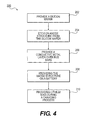
- FIG. 4 is a flowchart showing operations of providing an anode structure having lithiated silicon elements according to an example embodiment.
- FIG. 1 shows an example of a battery according to an example arrangement. Other arrangements may also be provided.
- FIG. 1 shows a battery 10 that includes an anode 12 (or anode structure) and a cathode 14 .
- the battery 10 may also include an electrolyte in a structure between the anode 12 and the cathode 14 .
- a separator may be provided between the anode 12 and the cathode 14 .
- the battery 10 may be used in an electronic device to provide stored energy to the electronic device.
- the anode or the cathode may be designed to store more energy.
- the electronic device may be any one of a mobile terminal, a mobile device, a mobile computing platform, a mobile platform, a laptop computer, a tablet, an ultra-mobile personal computer, a mobile Internet device, a smartphone, a personal digital assistant, a display device, a television (TV), etc.
- current may flow into the anode 12 (of the battery 10 ) from a power source, such as a battery charger or an AC/DC (alternate current/direct current) converter.
- the current may flow out from the cathode 14 (of the battery 10 ) in order to provide power (or energy) to other components, such as the load, of the electronic device.
- an anode or an anode structure may be made of carbon or graphite.
- the anode or the anode structure may be made of silicon. Silicon may have a much better energy absorption rate as compared to carbon or graphite. According, silicon may be used for the anode structure.
- lithium ions may be provided to the carbon structure.
- the ions may be provided between layers of the carbon, and the carbon may expand.
- lithium ions may be provided to the silicon structure.
- the ions may be incorporated into a lithium/silicon compound, and the silicon may expand at a greater rate. The expansion of the silicon may cause stress and fracture of silicon, and may lead to rapid degradation of a silicon anode as a battery cell component.
- Embodiments may provide an anode structure that may expand in a predictable manner in order to fill voids (or gaps) between silicon elements.
- the anode structure may be designed such that when the silicon elements are fully lithiated, then most of the voids may be closed out and the lithiated structure may approximate a solid block of fully lithiated silicon.
- Embodiments may provide a structure in which silicon elements may expand and contract in a predictable manner while avoiding (or reducing) fracturing.
- the battery may be “breathing” as the battery is being charged (lithium ions are inserted and the silicon elements expand) and the battery is being discharged (lithium ions extracted and the silicon elements are contracted).
- Embodiments may provide the silicon elements in a fixed pattern to form a plurality of voids in a fixed pattern.
- Embodiments may add lithium ions into a silicon structure such that the gaps or voids are filled (by expansion of the silicon or silicon elements).
- the lithium ions may be added to the silicon or silicon elements during a charging process.
- the silicon elements may expand into the voids (having the fixed pattern).
- FIG. 2 shows an anode structure having silicon elements according to an example embodiment. Other embodiments and configurations may also be provided.
- FIG. 2 shows an anode structure 120 that may correspond to the anode 12 ( FIG. 1 ).
- the anode structure 120 may include a first bus bar 52 (or first conductor) and a second bus bar 54 (or second conductor).
- the first bus bar 52 and the second bus bar 54 may be used to conduct electrons away from an anode structure.
- the first bus bar 52 may be a first metal conductor.
- the second bus bar 54 may be a second metal conductor.
- silicon elements 80 may be provided between the first bus bar 52 and the second bus bar 54 .
- the silicon elements 80 may be non-lithiated silicon.
- a tip of each portion of the silicon elements 80 may be coupled to either the first bus bar 52 or the second bus bar 54 .
- FIG. 2 shows silicon wedges that may be attached to the first or second bus bar 52 , 54 , such as a metal bar bus with a conductive metal coating.
- the silicon elements may be in a triangular shape, and may contact one of the bus bars 52 , 54 .
- FIG. 2 shows the silicon elements 80 includes first silicon element 81 , second silicon element 82 , third silicon element 83 , fourth silicon element 84 , fifth silicon element 85 , sixth silicon element 86 and seventh silicon element 87 .
- a tip of each of the first silicon element 81 , the third silicon element 83 , the fifth silicon element 85 and the seventh silicon element 87 may contact (or be coupled or attached) to the first bus bar 52 .
- a tip of each of the second silicon element 82 , the fourth silicon element 84 , and the sixth silicon element 86 may contact (or be coupled or attached) to the second bus bar 54 .
- FIG. 2 also shows that a void (or space) may be provided between the first silicon element 81 and the second silicon element 82 , a void (or space) may be provided between the second silicon element 82 and the third silicon element 83 , and a void (or space) may be provided between the third silicon element 83 and the fourth silicon element 84 .
- FIG. 2 also shows that a void (or space) may be provided between the fourth silicon element 85 and the fifth silicon element 85 , a void (or space) may be provided between the fifth silicon element 85 and the sixth silicon element 86 , and a void (or space) may be provided between the sixth silicon element 86 and the seventh silicon element 87 .
- Each of the first through seventh silicon elements 81 - 87 may be individually and separately called a silicon storage element (or silicon element).
- FIG. 3 shows an anode structure having lithiated silicon elements (or silicon) according to an example embodiment. Other embodiments and configurations may also be provided.
- FIG. 3 is intended to show that silicon elements may expand when lithiated (i.e., lithium ions are provided).
- the expansion may fill voids (or gaps) in the silicon (or silicon elements).
- the silicon elements (in the fixed pattern) may expand into the voids (in the fixed pattern).
- FIG. 3 shows an anode structure 130 that may correspond to the anode 12 ( FIG. 1 ).
- the anode structure 130 may include the first bus bar 52 and the second bus bar 54 .
- the first bus bar 52 and the second bus bar 54 may be used to conduct electrons away from the anode structure 130 .
- silicon elements may be provided between the first bus bar 52 and the second bus bar 54 , and then the silicon elements may be lithiated in order to provide lithiated silicon elements 180 between the first bus bar 52 and the second bus bar 54 .
- the silicon elements 180 may be lithiated from the silicon elements 80 of FIG. 2 .
- the lithiation of the silicon elements 80 may cause the silicon to expand and to fill the void (or space) between the respective silicon elements.
- FIG. 3 shows a reduced void (or space) between the first silicon element 181 and the second silicon element 182 , a reduced void (or space) between the second silicon element 182 and the third silicon element 183 , and a reduced void (or space) between the third silicon element 183 and the fourth silicon element 184 .
- FIG. 3 also shows that a reduced void (or space) between the fourth silicon element 184 and the fifth silicon element 185 , a reduced void (or space) between the fifth silicon element 185 and the sixth silicon element 186 , and a reduced void (or space) between the sixth silicon element 186 and the seventh silicon element 187 .
- the first through seventh silicon elements 181 - 187 may also be individually considered a silicon storage element.
- an anode structure may be obtained by etching a structure from a silicon wafer.
- a plurality of conductive bus bars may be provided as metal layers (such as the first and second conductors). The bus bars may then be protected from the lithiation by the conductive metal layer.
- the exposed anode storage elements i.e., the silicon elements
- the silicon anode may be used rather than a carbon anode.
- an array of expandable silicon elements may store the lithium ions received from the electrolyte during the charging process.
- a metal current collection (such as on right side of FIG. 1 ) may be replaced by a junction of bus bars (such as the first and second conductors 52 , 54 in FIG. 2 ).
- the bus bars at a micro level may be vertically provided, and may be joined at edges of the structure by a bus bar provided horizontally.
- FIG. 4 is a flowchart showing operations of providing an anode structure having lithiated silicon elements according to an example embodiment. Other operations, orders of operations and embodiments may also be provided.
- FIG. 4 is a flowchart 200 showing a methodology of providing a lithiation of a silicon anode structure.
- a silicon wafer may be provided.
- An anode structure (or a plurality of bus bars) may be etched in the silicon in operation 204 .
- a conductive metal layer may be provided over each of the bus bars in operation 206 .
- the anode structure may have at least two bus bars and a plurality of silicon elements.
- the anode structure and the cathode structure may be provided to form a battery in operation 208 .
- lithium ions may be provided to the silicon elements.
- the exposed silicon elements may expand into the voids based on the lithium ions. This may fill voids (or partially fill voids) between the silicon elements.
- Example 1 is an anode structure comprising: a first bus bar having a first conductive coating, a second bus bar having a second conductive coating, and a plurality of silicon elements between the first bus bar and the second bus bar with a first void between a first one of the silicon elements and a second one of the silicon elements, and at least the first one of the silicon elements to expand into the first void.
- Example 2 the subject matter of Example 1 can optionally include that the first one of the silicon elements to expand and to reduce the first void between the first one of the silicon elements and the second one of the silicon elements.
- Example 3 the subject matter of Example 1 can optionally include that the first one of the silicon elements to expand in response to receiving at least one lithium ion.
- Example 4 the subject matter of Example 1 and Example 3 can optionally include that the at least one lithium ion to be provided to the silicon elements during a charging process.
- Example 5 the subject matter of Example 1 can optionally include that the plurality of silicon elements include the second one of the silicon elements and a third one of the silicon elements with a second void between the second one of the silicon elements and the third one of the silicon elements, and the second one of the silicon elements to expand into the second void.
- Example 6 the subject matter of Example 1 and Example 6 can optionally include that the second one of the silicon elements to expand in response to receiving at least one lithium ion.
- Example 7 the subject matter of Example 1 can optionally include that the first one of the silicon elements is in a triangular shape, and the first one of the silicon elements to contact the first bus bar.
- Example 8 the subject matter of Example 1 and Example 7 can optionally include that the second one of the silicon elements is in a triangular shape, and the second one of the silicon elements to contact the second bus bar.
- Example 9 the subject matter of Example 1 and Example 7 can optionally include that the plurality of silicon elements are in a fixed pattern.
- Example 10 is a battery comprising: a cathode structure, and an anode structure including: a first bus bar, a second bus bar, and a plurality of silicon elements between the first bus bar and the second bus bar, and the plurality of silicon elements to form a first void between a first one of the silicon elements and a second one of the silicon elements, and at least the first one of the silicon elements to expand into the first void.
- Example 11 the subject matter of Example 10 and Example 3 can optionally include that the first one of the silicon elements to expand and to reduce the first void between the first one of the silicon elements and the second one of the silicon elements.
- Example 12 the subject matter of Example 10 can optionally include that the first one of the silicon elements to expand in response to receiving at least one lithium ion.
- Example 13 the subject matter of Example 10 and Example 12 can optionally include that the at least one lithium ion to be provided to the silicon elements during a charging process.
- Example 14 the subject matter of Example 10 can optionally include that the plurality of silicon elements to form a second void between the second one of the silicon elements and a third one of the silicon elements, and the second one of the silicon elements to expand into the second void.
- Example 15 the subject matter of Example 10 and Example 14 can optionally include that the second one of the silicon elements to expand in response to receiving at least one lithium ion.
- Example 16 the subject matter of Example 10 can optionally include that the first one of the silicon elements is in a triangular shape, and the first one of the silicon elements to contact the first bus bar.
- Example 17 the subject matter of Example 10 and Example 16 can optionally include that the second one of the silicon elements is in a triangular shape, and the second one of the silicon elements to contact the second bus bar.
- Example 18 the subject matter of Example 10 can optionally include that the plurality of silicon elements are in a fixed pattern.
- Example 19 is a method of a battery comprising: providing an anode structure having a first bus bar, a second bus bar, and a plurality of silicon elements with a first void between a first one of the silicon elements and a second one of the silicon elements, providing lithium ions to the silicon elements, and expanding at least the first one of the silicon elements into the first void.
- Example 20 the subject matter of Example 19 can optionally include that expanding at least the first one of the silicon elements to reduce the first void between the first one of the silicon elements and the second one of the silicon elements.
- Example 21 the subject matter of Example 19 can optionally include that expanding at least the first one of the silicon elements to occur in response to receiving at least one of the lithium ions.
- Example 22 the subject matter of Example 19 can optionally include that providing the lithium ions is to be provided during a charging process.
- Example 23 the subject matter of Example 19 can optionally include expanding at least the second one of the silicon elements into a second void between the second one of the silicon elements and a third one of the silicon elements.
- Example 24 the subject matter of Example 19 and Example 23 can optionally include that expanding at least the second one of the silicon elements to occur in response to receiving at least one of the lithium ions.
- Example 25 the subject matter of Example 19 can optionally include that the first one of the silicon elements is in a triangular shape, and the first one of the silicon elements to contact the first bus bar.
- Example 26 the subject matter of Example 19 and Example 25 can optionally include that the second one of the silicon elements is in a triangular shape, and the second one of the silicon elements to contact the second bus bar.
- Example 27 the subject matter of Example 19 can optionally include that the plurality of silicon elements are in a fixed pattern.
- Example 28 is a method of forming an anode structure, comprising: providing a silicon structure having a plurality of silicon elements with a first void between a first one of the silicon elements and a second one of the silicon elements, providing a first bus bar and a second bus bar at the silicon structure, providing a first conductive layer at the first bus bar, providing a second conductive layer at the second bus bar, and expanding at least a first one of the silicon elements into the first void between the first one of the silicon elements and the second one of the silicon elements.
- Example 29 the subject matter of Example 28 can optionally include that expanding at least the first one of the silicon elements to reduce the first void between the first one of the silicon elements and the second one of the silicon elements.
- Example 30 the subject matter of Example 28 and Example 29 can optionally include that expanding at least the first one of the silicon elements to occur in response to receiving at least one lithium ion.
- Example 31 the subject matter of Example 28 and Example 30 can optionally include that the at least one lithium ion to be provided during a charging process.
- Example 32 the subject matter of Example 28 can optionally include expanding at least the second one of the silicon elements into a second void between the second one of the silicon elements and a third one of the silicon elements.
- Example 33 the subject matter of Example 28 and Example 32 can optionally include that expanding at least the second one of the silicon elements to occur in response to receiving at least one lithium ion.
- Example 34 the subject matter of Example 28 can optionally include that the first one of the silicon elements is in a triangular shape, and the first one of the silicon elements to contact the first bus bar.
- Example 35 the subject matter of Example 28 and Example 34 can optionally include that the second one of the silicon elements is in a triangular shape, and the second one of the silicon elements to contact the second bus bar.
- Example 36 the subject matter of Example 28 can optionally include that the plurality of silicon elements are in a fixed pattern.
- Example 37 is an anode structure comprising: a first bus bar having a first conductive coating, a second bus bar having a second conductive coating, and a plurality of silicon elements provided in a fixed pattern between the first bus bar and the second bus bar to form a plurality of voids in a fixed pattern, at least a first one of the silicon elements to expand into a first one of the voids, and at least a second one of the silicon elements to expand into a second one of the voids.
- Example 38 the subject matter of Example 37 can optionally include that the first one of the silicon elements to expand and to reduce the first one of the voids, and the second one of the silicon elements to expand and to reduce the second one of the voids.
- Example 39 the subject matter of Example 37 can optionally include that the first one of the silicon elements to expand in response to receiving at least one lithium ion.
- Example 40 the subject matter of Example 37 and Example 39 can optionally include that the at least one lithium ion to be provided to the silicon elements during a charging process.
- Example 41 the subject matter of Example 37 can optionally include that the first one of the silicon elements is in a triangular shape, and the first one of the silicon elements to contact the first bus bar.
- Example 42 the subject matter of Example 37 and Example 41 can optionally include that the second one of the silicon elements is in a triangular shape, and the second one of the silicon elements to contact the second bus bar.
- any reference in this specification to “one embodiment,” “an embodiment,” “example embodiment,” etc. means that a particular feature, structure, or characteristic described in connection with the embodiment is included in at least one embodiment.
- the appearances of such phrases in various places in the specification are not necessarily all referring to the same embodiment.
Landscapes
- Chemical & Material Sciences (AREA)
- Chemical Kinetics & Catalysis (AREA)
- Electrochemistry (AREA)
- General Chemical & Material Sciences (AREA)
- Engineering & Computer Science (AREA)
- Materials Engineering (AREA)
- Manufacturing & Machinery (AREA)
- Battery Electrode And Active Subsutance (AREA)
- Secondary Cells (AREA)
- Battery Mounting, Suspending (AREA)
Abstract
Description
Claims (25)
Priority Applications (1)
| Application Number | Priority Date | Filing Date | Title |
|---|---|---|---|
| US14/142,789 US9537147B2 (en) | 2013-12-28 | 2013-12-28 | Anode structure having silicon elements |
Applications Claiming Priority (1)
| Application Number | Priority Date | Filing Date | Title |
|---|---|---|---|
| US14/142,789 US9537147B2 (en) | 2013-12-28 | 2013-12-28 | Anode structure having silicon elements |
Publications (2)
| Publication Number | Publication Date |
|---|---|
| US20150188130A1 US20150188130A1 (en) | 2015-07-02 |
| US9537147B2 true US9537147B2 (en) | 2017-01-03 |
Family
ID=53482904
Family Applications (1)
| Application Number | Title | Priority Date | Filing Date |
|---|---|---|---|
| US14/142,789 Expired - Fee Related US9537147B2 (en) | 2013-12-28 | 2013-12-28 | Anode structure having silicon elements |
Country Status (1)
| Country | Link |
|---|---|
| US (1) | US9537147B2 (en) |
Citations (8)
| Publication number | Priority date | Publication date | Assignee | Title |
|---|---|---|---|---|
| US20060115735A1 (en) * | 2003-04-23 | 2006-06-01 | Kiyotaka Yasuda | Negative electrode for nonaqueous electrolyte secondary battery, method for manufacturing same and nonaqueous electrolyte secondary battery |
| US20080122290A1 (en) | 2003-07-18 | 2008-05-29 | Li Peter T | Adapter power for mobile devices |
| US7751994B2 (en) | 2007-09-29 | 2010-07-06 | Intel Corporation | Intelligent battery safety management system configured to compare collected operational data with reference operational data |
| US7795843B2 (en) | 2007-12-28 | 2010-09-14 | Intel Corporation | Short circuit detection for batteries |
| US7852045B2 (en) | 2007-06-20 | 2010-12-14 | Intel Corporation | Battery charge management using a scheduling application |
| US20110234151A1 (en) | 2010-03-26 | 2011-09-29 | Uan-Zo-Li Alexander B | Platform with power boost |
| US8282774B2 (en) | 2005-05-02 | 2012-10-09 | International Paper Company | Ligno cellulosic materials and the products made therefrom |
| US8865345B1 (en) * | 2007-01-12 | 2014-10-21 | Enovix Corporation | Electrodes for three-dimensional lithium batteries and methods of manufacturing thereof |
-
2013
- 2013-12-28 US US14/142,789 patent/US9537147B2/en not_active Expired - Fee Related
Patent Citations (8)
| Publication number | Priority date | Publication date | Assignee | Title |
|---|---|---|---|---|
| US20060115735A1 (en) * | 2003-04-23 | 2006-06-01 | Kiyotaka Yasuda | Negative electrode for nonaqueous electrolyte secondary battery, method for manufacturing same and nonaqueous electrolyte secondary battery |
| US20080122290A1 (en) | 2003-07-18 | 2008-05-29 | Li Peter T | Adapter power for mobile devices |
| US8282774B2 (en) | 2005-05-02 | 2012-10-09 | International Paper Company | Ligno cellulosic materials and the products made therefrom |
| US8865345B1 (en) * | 2007-01-12 | 2014-10-21 | Enovix Corporation | Electrodes for three-dimensional lithium batteries and methods of manufacturing thereof |
| US7852045B2 (en) | 2007-06-20 | 2010-12-14 | Intel Corporation | Battery charge management using a scheduling application |
| US7751994B2 (en) | 2007-09-29 | 2010-07-06 | Intel Corporation | Intelligent battery safety management system configured to compare collected operational data with reference operational data |
| US7795843B2 (en) | 2007-12-28 | 2010-09-14 | Intel Corporation | Short circuit detection for batteries |
| US20110234151A1 (en) | 2010-03-26 | 2011-09-29 | Uan-Zo-Li Alexander B | Platform with power boost |
Non-Patent Citations (1)
| Title |
|---|
| Matthew T. McDowell et al.; "In Situ TEM of Two-Phase Lithiation of Amorphous Silicon Nanospheres;" Nano Letters, ACS Publications, dx.doi.org/10.1021/n13044508 /Nano Lett. XXXX, XXX, XXX-XX, pp. A-F. Received: Dec. 3, 2012, Revised Jan. 3, 2013. |
Also Published As
| Publication number | Publication date |
|---|---|
| US20150188130A1 (en) | 2015-07-02 |
Similar Documents
| Publication | Publication Date | Title |
|---|---|---|
| JP6498792B2 (en) | Battery charge limit prediction method, battery quick charge method and apparatus using the same | |
| Li et al. | Modeling the SEI-formation on graphite electrodes in LiFePO4 batteries | |
| Fan et al. | Modeling and theoretical design of next-generation lithium metal batteries | |
| Hasan et al. | Analysis of the implications of rapid charging on lithium-ion battery performance | |
| Suthar et al. | Effect of porosity, thickness and tortuosity on capacity fade of anode | |
| JP6523450B2 (en) | Battery quick charging method and apparatus | |
| Legrain et al. | Comparative computational study of the energetics of Li, Na, and Mg storage in amorphous and crystalline silicon | |
| JP5990619B2 (en) | Battery device having high energy density and high power density | |
| Hao et al. | Mesoscale analysis of the electrolyte-electrode interface in all-solid-state Li-ion batteries | |
| KR102441469B1 (en) | Battery charging method and battery charging device | |
| CN103117412B (en) | Lithium ion battery and chemical synthesizing method thereof | |
| CN105552305A (en) | Electrode for a combination of supercapacitor and battery and also process for the production thereof | |
| CN106532159A (en) | Battery charging method and device | |
| EP2789034B1 (en) | A mixture, a slurry for an electrode, a battery electrode, a battery and associated methods | |
| Ye et al. | Simulation and evaluation of capacity recovery methods for spiral-wound lithium ion batteries | |
| CN115377536B (en) | A battery charging and discharging method | |
| KR20130126344A (en) | Method for charging lithium secondary battery at low temperature | |
| US9537147B2 (en) | Anode structure having silicon elements | |
| Fu et al. | Intelligent dual-anode strategy for high-performance lithium-ion batteries | |
| US10476103B2 (en) | Electrode containing silicon and copolymer having ionic ally conductive polymer and electrically conductive polymer, and battery cell using same | |
| Cai et al. | Mathematical Modeling of a Lithium Ion Battery | |
| Pedersen et al. | The reversible lithiation of SnO: a three-phase process | |
| JP2016126949A (en) | Input/output recovery method and control system | |
| Jao et al. | Fast Discharging Stabilizes Electrochemical Interfaces: Achieving Close-to-Unity Reversibility in “Dendrite-Forming” Battery Electrodes | |
| WO2021184376A1 (en) | Method for improving battery cycle performance and electronic device |
Legal Events
| Date | Code | Title | Description |
|---|---|---|---|
| AS | Assignment |
Owner name: INTEL CORPORATION, CALIFORNIA Free format text: ASSIGNMENT OF ASSIGNORS INTEREST;ASSIGNOR:KEATES, ANDY;REEL/FRAME:032185/0716 Effective date: 20140107 |
|
| FEPP | Fee payment procedure |
Free format text: PAYOR NUMBER ASSIGNED (ORIGINAL EVENT CODE: ASPN); ENTITY STATUS OF PATENT OWNER: LARGE ENTITY |
|
| STCF | Information on status: patent grant |
Free format text: PATENTED CASE |
|
| MAFP | Maintenance fee payment |
Free format text: PAYMENT OF MAINTENANCE FEE, 4TH YEAR, LARGE ENTITY (ORIGINAL EVENT CODE: M1551); ENTITY STATUS OF PATENT OWNER: LARGE ENTITY Year of fee payment: 4 |
|
| FEPP | Fee payment procedure |
Free format text: MAINTENANCE FEE REMINDER MAILED (ORIGINAL EVENT CODE: REM.); ENTITY STATUS OF PATENT OWNER: LARGE ENTITY |
|
| LAPS | Lapse for failure to pay maintenance fees |
Free format text: PATENT EXPIRED FOR FAILURE TO PAY MAINTENANCE FEES (ORIGINAL EVENT CODE: EXP.); ENTITY STATUS OF PATENT OWNER: LARGE ENTITY |
|
| STCH | Information on status: patent discontinuation |
Free format text: PATENT EXPIRED DUE TO NONPAYMENT OF MAINTENANCE FEES UNDER 37 CFR 1.362 |
|
| FP | Lapsed due to failure to pay maintenance fee |
Effective date: 20250103 |