US9536894B2 - Non-volatile memory device - Google Patents
Non-volatile memory device Download PDFInfo
- Publication number
- US9536894B2 US9536894B2 US14/619,581 US201514619581A US9536894B2 US 9536894 B2 US9536894 B2 US 9536894B2 US 201514619581 A US201514619581 A US 201514619581A US 9536894 B2 US9536894 B2 US 9536894B2
- Authority
- US
- United States
- Prior art keywords
- memory
- channel body
- semiconductor layer
- crystal grain
- layer
- Prior art date
- Legal status (The legal status is an assumption and is not a legal conclusion. Google has not performed a legal analysis and makes no representation as to the accuracy of the status listed.)
- Active
Links
- 239000013078 crystal Substances 0.000 claims abstract description 72
- 239000004065 semiconductor Substances 0.000 claims abstract description 53
- 239000000463 material Substances 0.000 claims description 2
- 239000010410 layer Substances 0.000 description 86
- 239000011229 interlayer Substances 0.000 description 18
- VYPSYNLAJGMNEJ-UHFFFAOYSA-N Silicium dioxide Chemical compound O=[Si]=O VYPSYNLAJGMNEJ-UHFFFAOYSA-N 0.000 description 13
- 229910052814 silicon oxide Inorganic materials 0.000 description 13
- IJGRMHOSHXDMSA-UHFFFAOYSA-N Atomic nitrogen Chemical compound N#N IJGRMHOSHXDMSA-UHFFFAOYSA-N 0.000 description 8
- 229910021420 polycrystalline silicon Inorganic materials 0.000 description 7
- 229910052581 Si3N4 Inorganic materials 0.000 description 6
- 229920005591 polysilicon Polymers 0.000 description 6
- HQVNEWCFYHHQES-UHFFFAOYSA-N silicon nitride Chemical compound N12[Si]34N5[Si]62N3[Si]51N64 HQVNEWCFYHHQES-UHFFFAOYSA-N 0.000 description 6
- 239000000758 substrate Substances 0.000 description 6
- XUIMIQQOPSSXEZ-UHFFFAOYSA-N Silicon Chemical compound [Si] XUIMIQQOPSSXEZ-UHFFFAOYSA-N 0.000 description 5
- 239000012535 impurity Substances 0.000 description 5
- 238000001020 plasma etching Methods 0.000 description 5
- 229910052710 silicon Inorganic materials 0.000 description 5
- 239000010703 silicon Substances 0.000 description 5
- OKTJSMMVPCPJKN-UHFFFAOYSA-N Carbon Chemical compound [C] OKTJSMMVPCPJKN-UHFFFAOYSA-N 0.000 description 4
- 229910052799 carbon Inorganic materials 0.000 description 4
- 238000005229 chemical vapour deposition Methods 0.000 description 4
- 238000000151 deposition Methods 0.000 description 4
- 238000004519 manufacturing process Methods 0.000 description 4
- 230000004048 modification Effects 0.000 description 4
- 238000012986 modification Methods 0.000 description 4
- 229910052757 nitrogen Inorganic materials 0.000 description 4
- 238000003491 array Methods 0.000 description 2
- 239000004020 conductor Substances 0.000 description 2
- 238000005530 etching Methods 0.000 description 2
- 239000012212 insulator Substances 0.000 description 2
- 238000003860 storage Methods 0.000 description 2
- 230000005540 biological transmission Effects 0.000 description 1
- 230000007423 decrease Effects 0.000 description 1
- 230000000593 degrading effect Effects 0.000 description 1
- 238000010586 diagram Methods 0.000 description 1
- 238000003384 imaging method Methods 0.000 description 1
- 238000005468 ion implantation Methods 0.000 description 1
- 238000000034 method Methods 0.000 description 1
- 238000006467 substitution reaction Methods 0.000 description 1
- 238000003949 trap density measurement Methods 0.000 description 1
- 230000005641 tunneling Effects 0.000 description 1
Images


Classifications
-
- H01L27/11582—
-
- H01L27/1157—
-
- H—ELECTRICITY
- H01—ELECTRIC ELEMENTS
- H01L—SEMICONDUCTOR DEVICES NOT COVERED BY CLASS H10
- H01L29/00—Semiconductor devices adapted for rectifying, amplifying, oscillating or switching, or capacitors or resistors with at least one potential-jump barrier or surface barrier, e.g. PN junction depletion layer or carrier concentration layer; Details of semiconductor bodies or of electrodes thereof ; Multistep manufacturing processes therefor
- H01L29/02—Semiconductor bodies ; Multistep manufacturing processes therefor
- H01L29/04—Semiconductor bodies ; Multistep manufacturing processes therefor characterised by their crystalline structure, e.g. polycrystalline, cubic or particular orientation of crystalline planes
-
- H—ELECTRICITY
- H01—ELECTRIC ELEMENTS
- H01L—SEMICONDUCTOR DEVICES NOT COVERED BY CLASS H10
- H01L29/00—Semiconductor devices adapted for rectifying, amplifying, oscillating or switching, or capacitors or resistors with at least one potential-jump barrier or surface barrier, e.g. PN junction depletion layer or carrier concentration layer; Details of semiconductor bodies or of electrodes thereof ; Multistep manufacturing processes therefor
- H01L29/02—Semiconductor bodies ; Multistep manufacturing processes therefor
- H01L29/06—Semiconductor bodies ; Multistep manufacturing processes therefor characterised by their shape; characterised by the shapes, relative sizes, or dispositions of the semiconductor regions ; characterised by the concentration or distribution of impurities within semiconductor regions
- H01L29/10—Semiconductor bodies ; Multistep manufacturing processes therefor characterised by their shape; characterised by the shapes, relative sizes, or dispositions of the semiconductor regions ; characterised by the concentration or distribution of impurities within semiconductor regions with semiconductor regions connected to an electrode not carrying current to be rectified, amplified or switched and such electrode being part of a semiconductor device which comprises three or more electrodes
- H01L29/1025—Channel region of field-effect devices
- H01L29/1029—Channel region of field-effect devices of field-effect transistors
- H01L29/1033—Channel region of field-effect devices of field-effect transistors with insulated gate, e.g. characterised by the length, the width, the geometric contour or the doping structure
-
- H—ELECTRICITY
- H10—SEMICONDUCTOR DEVICES; ELECTRIC SOLID-STATE DEVICES NOT OTHERWISE PROVIDED FOR
- H10B—ELECTRONIC MEMORY DEVICES
- H10B43/00—EEPROM devices comprising charge-trapping gate insulators
- H10B43/20—EEPROM devices comprising charge-trapping gate insulators characterised by three-dimensional arrangements, e.g. with cells on different height levels
- H10B43/23—EEPROM devices comprising charge-trapping gate insulators characterised by three-dimensional arrangements, e.g. with cells on different height levels with source and drain on different levels, e.g. with sloping channels
- H10B43/27—EEPROM devices comprising charge-trapping gate insulators characterised by three-dimensional arrangements, e.g. with cells on different height levels with source and drain on different levels, e.g. with sloping channels the channels comprising vertical portions, e.g. U-shaped channels
-
- H—ELECTRICITY
- H10—SEMICONDUCTOR DEVICES; ELECTRIC SOLID-STATE DEVICES NOT OTHERWISE PROVIDED FOR
- H10B—ELECTRONIC MEMORY DEVICES
- H10B43/00—EEPROM devices comprising charge-trapping gate insulators
- H10B43/30—EEPROM devices comprising charge-trapping gate insulators characterised by the memory core region
- H10B43/35—EEPROM devices comprising charge-trapping gate insulators characterised by the memory core region with cell select transistors, e.g. NAND
Definitions
- Embodiments are generally related to a non-volatile memory device.
- the memory cell array having the three-dimensional structure includes multiple word lines that are stacked and a NAND string that is formed in a memory hole extending through the multiple word lines.
- erasing data is performed collectively by memory cell block. Also, it is desirable to improve the data erasing characteristics as the memory capacity is increased.
- FIG. 1 is an exemplary cross-sectional view schematically showing a memory cell array of a non-volatile memory device according to a first embodiment
- FIG. 2 is an exemplary view schematically showing a constitution of the non-volatile memory device according to the first embodiment
- FIGS. 3A to 3L are exemplary cross-sectional views schematically showing manufacturing processes of the memory cell array according to the first embodiment
- FIGS. 4A and 4B are cross-sectional views schematically showing memory cell arrays according to variations of the first embodiment
- FIGS. 5A and 5B are schematic cross-sectional views showing a channel body of the memory cell array according to the first embodiment
- FIG. 6 is an exemplary cross-sectional view schematically showing a memory cell array according to a second embodiment
- FIG. 7 is a schematic perspective view showing a memory cell array according to the third embodiment.
- FIGS. 8A and 8B are schematic cross-sectional views showing a channel body of the memory cell array according to the third embodiment.
- a non-volatile memory device includes first electrodes arranged in a first direction, a second electrode disposed on a side of the first electrodes in the first direction, a semiconductor layer extending in the first direction through the first electrodes and the second electrode, and a memory film provided between the semiconductor layer and each of the first electrodes.
- the semiconductor layer includes crystal grains and has a first portion and a second portion, the first portion being adjacent to the first electrodes, and the second portion being adjacent to at least a part of the second electrode, wherein the first portion includes a larger crystal grain than a crystal grain in the second portion.
- FIG. 1 and FIG. 2 are schematic views showing a non-volatile memory device 100 according to a first embodiment.
- FIG. 1 is a cross-sectional view showing a memory cell array 1 of the non-volatile memory device 100 .
- the memory cell array 1 includes multiple first electrodes (hereinbelow, word lines 20 ), a second electrode (hereinbelow, a selection gate 30 ), and a third electrode (hereinbelow, a selection gate 40 ) that are provided on a first interconnect (hereinbelow, a source layer 10 ).
- the selection gate 40 , the multiple word lines 20 , and the selection gate 30 are disposed to be arranged in this order in a first direction (hereinbelow, the Z-direction) perpendicular to the source layer 10 .
- a second interconnect (a bit line 50 ) is provided on the side of the selection gate 30 opposite to the word lines 20 .
- the selection gate 30 is disposed between a word line 20 a and the bit line 50 .
- the selection gate 40 is disposed between the source layer 10 and a word line 20 b .
- the word line 20 a is positioned at the end of the multiple word lines 20 on the bit line 50 side.
- the word line 20 b is positioned at the end of the multiple word lines 20 on the source layer 10 side.
- An insulating film 23 is provided between the word lines 20 adjacent to each other in the Z-direction. Also, the Insulating film 23 is provided between the word line 20 a and the selection gate 30 , between the word line 20 b and the selection gate 40 , and between the source layer 10 and the selection gate 40 . The insulating film 23 electrically insulates the multiple word lines 20 , the selection gates 30 and 40 , and the source layer 10 .
- the memory cell array 1 further includes a semiconductor layer (hereinbelow, a channel body 60 ) and a memory film 70 that extend in the Z-direction from the source layer 10 toward the selection gate 30 .
- the channel body 60 extends through the selection gate 40 , the multiple word lines 20 , and the selection gate 30 in the Z-direction.
- the memory film 70 is provided between the channel body 60 and each of the multiple word lines 20 .
- the memory film 70 extends in the Z-direction along the channel body 60 . Also, the memory film 70 extends between the selection gate 30 and the channel body 60 and between the selection gate 40 and the channel body 60 .
- the memory film 70 is provided to cover the inner wall of a memory hole 80 piercing through the multiple word lines 20 , the selection gate 30 , and the selection gate 40 .
- the channel body 60 is provided on the memory film 70 and covers the wall surface and a bottom surface 80 b of the memory hole 80 .
- the channel body 60 is electrically connected to the source layer 10 at the bottom surface 80 b of the memory hole 80 .
- a core 90 is provided in the memory hole 80 .
- the core 90 is an insulator.
- the channel body 60 is positioned between the core 90 and the memory film 70 .
- the channel body 60 includes a first portion 61 and a second portion 63 .
- the second portion 63 is provided on the first portion 61 in the Z-direction.
- the first portion 61 opposes each of the multiple word lines 20 with the memory film 70 .
- the memory film 70 is interposed between the first portion 61 and each of the multiple word lines 20 .
- the second portion 63 opposes at least a part of the selection gate 30 .
- the channel body 60 includes a boundary 60 J between the first portion 61 and the second portion 63 . Also, the boundary 60 j is positioned in a portion of the channel body 60 opposing the selection gate 30 .
- the channel body 60 is, for example, a polycrystalline semiconductor including multiple crystal grains.
- the channel body 60 is, for example, polysilicon and includes crystal grains of silicon.
- the crystal grain size of the first portion 61 is larger than the crystal grain size of the second portion 63 .
- the “crystal grain size” is the average diameter of the crystal grains included in the channel body in this specification, if there is no comment thereon.
- the crystal grain size is the diameter in the case where a crystal grain of any shape is approximated as a sphere.
- the crystal grain size may be expressed as an average crystal grain size.
- the crystal grain size of a semiconductor material such as silicon, etc. can be measured by, for example, a transmission electron microscope (TEM).
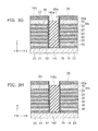
- FIGS. 5A and 5B are schematic views showing the channel body 60 , the memory film 70 and the core 90 which are embedded in the memory hole 80 .
- FIGS. 5A and 5B also are schematic cross-sectional views of the memory hole 80 in parallel with the X-Z plane.
- FIG. 5A is the cross-sectional view of a portion of the memory hole 80 that includes the second portion 63 of the channel body 60 .
- FIG. 5B is the cross-sectional view of a portion of the memory hole 80 that includes the first portion 61 of the channel body 60 .
- the channel body 60 includes crystal grains CG as shown in FIGS. 5A and 5B .
- a dashed portion of each crystal grains CG which is located outside the channel body 60 , is a hypothetical portion illustrated for imaging a crystal grain, and thus, not actually exists.
- the boundaries between the crystal grains are shown in FIGS. 5A and 5B as the grain boundary CB.
- the thickness of the channel body 60 in a second direction (e.g., an X-direction) perpendicular to the Z-direction is about 20 nanometers (nm).
- the crystal grain size RC 1 of the first portion 61 is, for example, about 200 nm; and the crystal grain size RC 2 of the second portion 63 is about 100 nm.
- the crystal grain boundaries CB of the channel body 60 are observed as discrete interfaces intersecting the Z-direction.
- the average spacing WR 1 in the Z-direction of the crystal grain boundaries of the first portion 61 is wider than the average spacing WR 2 in the Z-direction of the crystal grain boundaries of the second portion 63 .
- the channel body 60 includes a PN junction 60 j in a part of the second portion 63 that is adjacent to the select gate 30 .
- the channel body 60 includes at least one crystal boundary CB in the vicinity of the PN junction 60 J.
- the channel body 60 may include, for example, a PN junction 60 j positioned at the boundary between the first portion 61 and the second portion 63 .
- the first portion 61 has a P-type conductivity; and the second portion 63 has an N-type conductivity.
- the PN junction 60 J may be an interface between the crystal grains of the first portion 61 and the crystal grains of the second portion 63 .
- the channel body 60 may include a crystal grain boundary positioned at the vicinity of the PN junction.
- the memory cell array 1 includes multiple memory cells MC disposed in the Z-direction.
- the memory cells MC include portions of the memory film 70 and are provided between the channel body 60 and the word lines 20 .
- the memory cells MC are arranged in the extension direction (the Z-direction) of the channel body 60 .
- the number of memory cells provided in one memory hole 80 is equal to the number of stacks of word lines 20 .
- the memory film 70 extends in the Z-direction.
- the memory film 70 has, for example, a structure in which a silicon oxide film, a silicon nitride film, and a silicon oxide film are stacked in order.
- the silicon nitride film acts as, for example, a charge storage layer.
- the memory film 70 is not limited to the example recited above and may be, for example, a conductor provided between the channel body 60 and the word lines 20 and may have a structure including a charge storage layer made of a conductor disposed discretely in the Z-direction.
- the memory cell array 1 includes a selection transistor ST 1 and a selection transistor ST 2 .
- the selection transistor ST 1 includes the selection gate 30 , the channel body 60 , and the memory film 70 .
- the selection transistor ST 2 includes the selection gate 40 , the channel body 60 , and the memory film 70 .
- the selection gates 30 and 40 each act as a gate electrode.
- the channel body 60 acts as the channel of a transistor.
- the memory film 70 acts as the gate insulator film.
- the memory cell array 1 includes an interconnect layer 110 .
- the interconnect layer 110 is provided on the selection gate 30 with an inter-layer insulating film 25 interposed.
- the Interconnect layer 110 includes the bit line 50 , a contact plug 53 , and an insulating film 55 .
- the bit line 50 and the contact plug 53 are provided inside the insulating film 55 .
- the bit line 50 is electrically connected to the channel body 60 via the contact plug 53 .
- the memory cell array 1 includes a memory string in the memory hole 80 .
- the memory string includes the multiple memory cells MC disposed between the two selection transistors ST 1 and ST 2 . Also, one end of the memory string is electrically connected to the source layer 10 ; and the other end of the memory string is electrically connected to the bit line 50 .
- FIG. 2 is a block diagram showing the non-volatile memory device 100 according to the first embodiment.
- the non-volatile memory device 100 includes, for example, the memory cell array 1 , a row decoder 101 , a sense amplifier 103 , a control circuit 105 , and an interface 107 .
- the control circuit 105 controls the row decoder 101 and the sense amplifier 103 based on instructions acquired from the outside via the interface 107 .
- the control circuit 105 records information in the memory cells MC and reads the information from the memory cells MC via the row decoder 101 and the sense amplifier 103 .
- the memory cell array 1 includes multiple stacked bodies 130 .
- Each of the stacked bodies 130 includes the multiple word lines 20 and the selection gates 30 and 40 .
- the stacked bodies 130 are provided in rectangular configurations extending in the Y-direction.
- the stacked bodies 130 are disposed in the X-direction.
- Each of the stacked bodies 130 includes the multiple memory holes 80 .
- the row decoder 101 is connected to each of the multiple word lines 20 , the selection gate 30 , and the selection gate 40 and applies voltages to each.
- the sense amplifier 103 is connected to the multiple bit lines 50 and the source layer 10 , applies voltages between the source layer 10 and the bit lines 50 , and senses currents flowing between the source layer 10 and the bit lines 50 . Thereby, the sense amplifier 103 reads the data from the memory cells. Also, the sense amplifier 103 discriminates the data read from the memory cells MC and can store the data temporarily therein.
- bit line 50 extends in the X-direction and is electrically connected to the channel body 60 provided in one of the multiple memory holes 80 in each of the stacked bodies 130 .
- control circuit 105 can access one memory cell MC by selecting one word line 20 via the row decoder 101 and by selecting one bit line 50 via the sense amplifier 103 .
- control circuit 105 when erasing the data stored in the memory cells MC, the control circuit 105 erases all of the data stored in a memory block unit including multiple memory strings.
- Verase e.g., 20 V
- the source layer 10 is set to be floating.
- a GIDL current Gate Induced Drain Leak current
- the potential of the first portion 61 becomes a value near Verase.
- the electrons are removed from the memory film 70 or the holes are injected inside the memory film 70 , canceling charges that are stored in the memory cells MC inside the whole memory block. Thereby, the data of all of the memory cells in the memory block is erased.
- the density of the crystal grain boundaries is increased by reducing the crystal grain size of the second portion 63 .
- Carrier traps (inter-band levels) are formed at the crystal grain boundaries. Accordingly, the carrier trap density of the second portion 63 may be increased. For example, the density of the carrier traps are also increased at the vicinity of the PN junction provided in the second portion 63 .
- the generation of holes due to band-to-band tunneling via the carrier traps may be promoted when the PN junction is set to have a reverse bias.
- the supply of the holes to the first portion 61 can be increased by increasing the GIDL current of the selection transistor ST 1 .
- the reduction of the data erase time and the reliable data erasure of the selected memory block are realized; and thus, it is possible to improve the data erasing characteristics.
- the amount of carrier traps is suppressed by increasing the crystal grain size. Thereby, the erasing characteristics can be improved without degrading the performance of the memory cells MC.
- FIGS. 3A to 3L are schematic cross-sectional views showing an example of the manufacturing processes of the memory cell array 1 .
- the insulating film 23 and a conductive layer 121 are formed in this order on the source layer 10 .
- the insulating films 23 and conductive layers 123 are stacked alternately on the conductive layer 121 .
- Each of the multiple conductive layers 123 is stacked in the Z-direction with the insulating film 23 interposed.
- the number of stacks of conductive layers 123 is equal to the number of memory cells MC disposed in the Z-direction.
- a conductive layer 125 is formed on the insulating film 23 of the uppermost layer.
- the source layer 10 is formed on a substrate (not-shown).
- the substrate is, for example, a silicon substrate; and the source layer 10 is formed on the silicon substrate with an inter-layer insulating film interposed.
- the conductive layers 121 , 123 , and 125 are, for example, polycrystalline silicon (polysilicon) layers that have conductivity.
- the insulating films 23 are, for example, silicon oxide films.
- the source layer 10 may be formed by diffusing an Impurity, etc., into a semiconductor substrate.
- the stacked bodies 130 that have stripe configurations are formed by dividing the conductive layers 121 , 123 , and 125 by a trench 120 extending in the Y-direction (referring to FIG. 2 ).
- the conductive layers 121 , 123 , and 125 are formed into the selection gate 40 , the word lines 20 , and the selection gate 30 .
- the inter-layer insulating film 25 is formed to cover the stacked bodies 130 .
- the inter-layer insulating film 25 covers the selection gate 40 , the word lines 20 , and the selection gate 30 and fills the trench 120 .
- the inter-layer insulating film 25 is, for example, a silicon oxide film.
- to cover is not limited to the case where the “component that covers” directly contacts the “component that is covered” and includes the case where the “component that covers” covers the “component that is covered” with another component interposed.
- the memory hole 80 is made as shown in FIG. 3C .
- a through-hole is made from the upper surface of the inter-layer insulating film 25 to the source layer 10 using RIE (Reactive Ion Etching).
- RIE Reactive Ion Etching
- the memory hole 80 extends through the selection gate 40 , the multiple word lines 20 , and the selection gate 30 in the Z-direction.
- the memory film 70 that covers the inner wall of the memory hole 80 is formed.
- the memory film 70 is, for example, a stacked film including a silicon oxide film and a silicon nitride film.
- a silicon oxide film that covers the inner surface of the memory hole 80 and the upper surface of the inter-layer insulating film 25 is formed using CVD (Chemical Vapor Deposition).
- CVD Chemical Vapor Deposition
- a silicon nitride film is formed on the silicon oxide film; and another silicon oxide film is further formed on the silicon nitride film.
- the memory film 70 has, for example, a three-layer structure of the silicon oxide film/silicon nitride film/silicon oxide film.
- the memory film 70 is made conformally on the inner wall of the memory hole 80 .
- a memory film 70 a that is formed on the inter-layer insulating film 25 and a memory film 70 b that is formed on the bottom surface 80 b of the memory hole 80 are selectively removed (referring to FIG. 3D ).
- the memory films 70 a and 70 b are selectively removed using anisotropic RIE; and the portion that is formed on the wall surface of the memory hole 80 remains.
- the source layer 10 is exposed at the bottom surface 80 b of the memory hole 80 .
- a semiconductor layer 161 that covers the inter-layer insulating film 25 and the inner surface of the memory hole 80 is formed.
- the semiconductor layer 161 is, for example, a polysilicon layer formed using CVD.
- the semiconductor layer 161 includes, for example, a P-type impurity.
- the semiconductor layer 161 may be an undoped layer.
- the semiconductor layer 161 includes a portion 161 a contacting the source layer 10 exposed at the bottom surface 80 b of the memory hole 80 . Thereby, the semiconductor layer 161 is electrically connected to the source layer 10 .
- the insulating film 140 that fills the interior of the memory hole 80 is formed.
- the insulating film 140 is formed also on the inter-layer insulating film 25 .
- the insulating film 140 is, for example, a silicon oxide film.
- etch-back of the insulating film 140 is performed.
- the portion that is formed on the Inter-layer insulating film 25 and in an upper portion 80 a of the memory hole 80 is removed.
- the semiconductor layer 161 that is formed on the inter-layer insulating film 25 and the semiconductor layer 161 that is formed in the upper portion 80 a of the memory hole 80 are exposed.
- an upper surface 140 a of the insulating film 140 after the etchback is positioned at a level between an upper surface 30 a and a lower surface 30 b of the selection gate 30 .
- “level” is the position in the Z-direction and means, for example, the height from the upper surface of the source layer 10 .
- the semiconductor layer 161 that is exposed at the inter-layer insulating film 25 and the upper portion 80 a of the memory hole 80 is removed by etching.
- the first portion 61 of the channel body 60 is formed in the memory hole 80 .
- the first portion 61 extends between the insulating film 140 and the memory film 70 ; and the upper end of the first portion 61 is positioned at a level between the upper surface 30 a and the lower surface 30 b of the selection gate 30 .
- a semiconductor layer 163 that covers the inter-layer insulating film 25 and the upper portion 80 a of the memory hole 80 is formed.
- the semiconductor layer 163 is, for example, a polysilicon layer formed using CVD.
- the semiconductor layer 163 is formed so that the crystal grain size of the semiconductor layer 163 is smaller than the crystal grain size of the semiconductor layer 161 .
- carbon (C) or nitrogen (N) is doped when depositing the polysilicon. Thereby, the average crystal grain size of the semiconductor layer 163 is smaller than that of the case where carbon or nitrogen is not doped.
- an N-type impurity is doped into the semiconductor layer 163 .
- the N-type impurity may be doped when depositing the semiconductor layer 163 .
- ion implantation of the N-type impurity may be performed after depositing the semiconductor layer 163 .
- a portion 163 a that is formed on the insulating film 140 of the semiconductor layer 163 and a portion 163 b that is formed on the inter-layer insulating film 25 are selectively removed.
- selective etching is performed using anisotropic RIE (Reactive Ion Etching).
- anisotropic RIE Reactive Ion Etching
- the second portion 63 of the channel body 60 contacts the first portion 61 at the level of the upper surface 140 a of the insulating film 140 .
- the boundary between the first portion 61 and the second portion 63 is positioned at the level between the upper surface 30 a and the lower surface 30 b of the selection gate 30 .
- a PN junction is formed at the boundary between the first portion 61 and the second portion 63 .
- the crystal grains of the first portion 61 contact the crystal grains of the second portion 63 at the boundary between the first portion 61 and the second portion 63 . Accordingly, crystal grain boundaries exist at the boundary between the first portion 61 and the second portion 63 .
- the channel body 60 includes crystal grain boundaries at the vicinity of the PN junction.
- an insulating film 150 that fills the upper portion 80 a of the memory hole 80 is formed.
- the insulating film 150 is formed also on the inter-layer insulating film 25 .
- the insulating film 150 is, for example, a silicon oxide film.
- the insulating film 150 becomes a single body with the insulating film 140 to form the core 90 .
- the bit line 50 is formed on the insulating film 150 .
- the bit line 50 is electrically connected to the channel body 60 via the contact plug 53 formed inside the insulating film 150 .
- the insulating film 55 is formed on the bit line 50 .
- the insulating film 55 is an inter-layer insulating film covering the bit line 50 .
- the insulating film 55 becomes a single body with the insulating film 150 provided on the inter-layer insulating film 25 . Thereby, the memory cell array 1 is completed.
- the semiconductor layer 161 that includes a first crystal grain size and the semiconductor layer 163 that includes a second crystal grain size that is smaller than the first crystal grain size are formed in order.
- the channel body 60 that includes the first portion 61 and the second portion 63 can be formed.
- the embodiment is not limited to the example recited above. Memory cell arrays 2 and 3 according to modifications of the embodiment will now be illustrated.
- FIG. 4A is a schematic cross-sectional view showing the memory cell array 2 according to a first modification of the first embodiment.
- the memory cell array 2 includes a channel body 170 .
- the channel body 170 includes a first portion 171 and a second portion 173 .
- the second portion 173 includes a first conductivity-type unit 173 a and a second conductivity-type unit 173 b.
- the second portion 173 is provided on the first portion 171 in the Z-direction.
- the boundary between the first portion 171 and the second portion 173 is positioned at a level between the word line 20 a and the selection gate 30 .
- the word line 20 a is positioned at the end of the multiple word lines on the selection gate 30 side.
- the second conductivity-type unit 173 b is provided on the first conductivity-type unit 173 a .
- the boundary between the first conductivity-type unit 173 a and the second conductivity-type unit 173 b is positioned at a level between the upper surface 30 a and the lower surface 30 b of the selection gate 30 .
- the first conductivity type is the P-type
- the second conductivity type is the N-type.
- the position of the boundary between the first portion 171 and the second portion 173 and the position of the PN junction are different.
- the PN junction is provided in the second portion 173 having the crystal grain size that is smaller than that of the first portion 171 .
- crystal grain boundaries are included at the vicinity of the PN junction; and the GIDL current can be increased in the erasing operation of the memory cell array 2 .
- the boundary between the first portion 61 and the second portion 63 is formed to be different in the position from the PN junction.
- the PN junction is formed to be positioned inside the second portion 63 .
- FIG. 4B is a schematic cross-sectional view showing the memory cell array 3 according to a second modification of the first embodiment.
- the memory cell array 3 includes a channel body 180 .
- the channel body 180 includes a first portion 181 and a second portion 183 .
- the second portion 183 includes a first conductivity-type unit 183 a and a second conductivity-type unit 183 b .
- the core 90 is not provided.
- the second portion 183 is provided on the first portion 181 in the Z-direction.
- the boundary between the first portion 181 and the second portion 183 is positioned at a level between the word line 20 a and the selection gate 30 .
- the word line 20 a is positioned at the end of the multiple word lines 20 on the selection gate 30 side.
- the second conductivity-type unit 183 b is provided on the first conductivity-type unit 183 a .
- the boundary between the first conductivity-type unit 173 a and the second conductivity-type unit 173 b is positioned at a level between the upper surface 30 a and the lower surface 30 b of the selection gate 30 .
- the first conductivity type is the P-type
- the second conductivity type is the N-type.
- each of the first portion 181 and the second portion 183 are formed to fill a memory hole 185 .
- the memory hole 185 is filled with a first semiconductor layer used to form the first portion 181 .
- etch-back of the first semiconductor layer is performed; and a space where the second portion 183 is formed is provided in the upper portion of the memory hole 185 .
- the space of the upper portion of the memory hole 185 is filled by forming the second semiconductor layer that is used to form the second portion 183 .
- the second semiconductor layer is formed so that the crystal grain size of the second semiconductor layer is smaller than the crystal grain size of the first semiconductor layer. Also, the second semiconductor layer may be formed so that the crystal grain size of the second semiconductor layer gradually decreases in the stacking direction. For example, the amount of the carbon or nitrogen that is added is gradually increased when depositing the polysilicon.
- the carbon or nitrogen may be added while forming a portion of the second semiconductor layer in the vicinity of the PN junction.
- the crystal grain size becomes smaller in the vicinity of the PN junction, and becomes larger as increasing a distance to the PN junction.
- the position of the PN junction is different from the position of the boundary between the first portion 181 and the second portion 183 .
- the PN junction is provided in the second portion 183 having the crystal grain size that is smaller than that of the first portion 181 .
- the crystal grain boundaries are included at the vicinity of the PN junction; and the GIDL current can be increased in the erasing operation of the memory cell array 2 .
- FIG. 6 is a schematic cross-sectional view showing a memory cell array 4 according to a second embodiment.
- the memory cell array 4 includes a selection gate 190 .
- the selection gate 190 includes multiple sub-layers 191 , 193 , 195 , and 197 stacked in the Z-direction.
- the number of sub-layers included in the selection gate 190 is not limited to that of the example and may be, for example, two, three, five, or more.
- An insulating film 27 is formed between each of the sub-layers.
- the insulating film 27 is, for example, a silicon oxide film.
- the sub-layers are electrically connected to each other at not-shown portions.
- the channel body 60 includes the first portion 61 and the second portion 63 .
- the crystal grain size of the second portion 63 is smaller than the crystal grain size of the first portion 61 .
- the second portion 63 is adjacent to at least one of the multiple sub-layers. For example, the boundary 60 j between the first portion 61 and the second portion 63 is positioned at a level between the sublayer 195 and the sublayer 197 in the Z-direction.
- the first portion 61 has the N-type conductivity; and the second portion 63 has the P-type conductivity.
- the channel body 60 includes a PN junction; and the position of the PN junction matches the boundary 60 j between the first portion 61 and the second portion 63 .
- the PN junction of the channel body 60 may not match the boundary 60 j .
- the boundary 60 j may be positioned between the sub-layer 193 and the sub-layer 195 ; and the PN junction may be positioned inside the portion adjacent to the sub-layer 197 of the second portion 63 .
- the PN junction is provided in the second portion 63 having the crystal grain size that is smaller than that of the first portion 61 . Thereby, crystal grain boundaries are included at the vicinity of the PN junction; and the GIDL current can be increased in the erasing operation of the memory cell array 4 .
- FIG. 7 is a perspective view schematically showing a nonvolatile memory device 200 according to a third embodiment.
- the nonvolatile memory device 200 includes a memory cell array 5 having a three-dimensional structure.
- the nonvolatile memory device 200 includes, for example, a memory cell array 5 provided on a silicon substrate 201 with a back gate layer 203 interposed therebetween.
- the memory cell array 5 includes multiple word lines 210 and selection gates 220 stacked in the Z-direction. Also, the word lines 210 and the selection gates 220 are arranged in the X-direction. Further, the memory cell array 5 includes semiconductor pillars 230 extending through the word lines 210 and the selection gates 220 stacked in the Z-direction.
- two semiconductor pillars 230 that are adjacent to each other in the X-direction are connected by a pipe connection (PC) 240 in the back gate layer 203 . Then, one end of the semiconductor pillars 230 connected via the PC 240 is electrically connected to a bit line BL. Also, the other end of the semiconductor pillars 230 is electrically connected to a source line SL.
- PC pipe connection
- Memory cells MC are formed at the portions where the semiconductor pillars 230 extend through each of the word lines 210 . Also, selection transistors are formed between the selection gates 220 and the semiconductor pillars 230 . Thereby, a memory string MS is provided along the two mutually-adjacent semiconductor pillars 230 .
- Each semiconductor pillar 230 includes, for example, a channel body 60 , a memory film 70 and core 90 (see FIGS. 5A and 5B ).
- the channel body 60 includes a plurality of crystal grains, wherein a crystal grain size in the first portion 61 is larger than a crystal grain size in the second portion 63 .
- the first portion 61 is adjacent to the word lines 210
- the second portion 63 is adjacent to at least a part of the selection gate 220 , thereby increasing the GIDL current when erasing data in the memory cell array 5 .
- FIGS. 8A and 8B are schematic perspective views showing the channel body 60 , the memory film 70 and the core 90 which are embedded in the memory hole.
- FIGS. 8A and 8B also are schematic cross-sectional views of the memory hole in parallel with the X-Y plane.
- FIG. 8A is the cross-sectional view of a portion of the memory hole that includes the first portion 61 of the channel body 60 .
- FIG. 8B is the cross-sectional view of a portion of the memory hole that includes the second portion 63 of the channel body 60 .
- the cross sections of the channel body 60 in FIGS. 8A and 8B include the crystal grain boundaries CB.
- the crystal grain boundaries CB have distance W R1 or W R2 therebetween in FIGS. 8A and 8B respectively, which is defined as a distance along the periphery of the channel body 60 .
- the crystal grain size in the first portion 61 is larger than the crystal grain size in the second portion 63 , and thus, the average of the distance W R1 in the first portion 61 in FIG. 8B is wider than the average of the distance W R2 in the second portion 63 in FIG. 8A .
Abstract
Description
Claims (1)
Priority Applications (1)
| Application Number | Priority Date | Filing Date | Title |
|---|---|---|---|
| US14/619,581 US9536894B2 (en) | 2014-08-04 | 2015-02-11 | Non-volatile memory device |
Applications Claiming Priority (2)
| Application Number | Priority Date | Filing Date | Title |
|---|---|---|---|
| US201462032669P | 2014-08-04 | 2014-08-04 | |
| US14/619,581 US9536894B2 (en) | 2014-08-04 | 2015-02-11 | Non-volatile memory device |
Publications (2)
| Publication Number | Publication Date |
|---|---|
| US20160035741A1 US20160035741A1 (en) | 2016-02-04 |
| US9536894B2 true US9536894B2 (en) | 2017-01-03 |
Family
ID=55180841
Family Applications (1)
| Application Number | Title | Priority Date | Filing Date |
|---|---|---|---|
| US14/619,581 Active US9536894B2 (en) | 2014-08-04 | 2015-02-11 | Non-volatile memory device |
Country Status (1)
| Country | Link |
|---|---|
| US (1) | US9536894B2 (en) |
Cited By (5)
| Publication number | Priority date | Publication date | Assignee | Title |
|---|---|---|---|---|
| US10971513B2 (en) | 2018-07-16 | 2021-04-06 | Samsung Electronics Co., Ltd. | Three-dimensional semiconductor memory devices and method of manufacturing the same |
| US11114457B2 (en) | 2019-05-13 | 2021-09-07 | SK Hynix Inc. | Semiconductor device and manufacturing method of the semiconductor device |
| US11201166B2 (en) | 2019-05-31 | 2021-12-14 | Samsung Electronics Co., Ltd. | Three dimensional semiconductor device including first and second channels and buried insulation and conductive patterns and method of manufacturing the same |
| US11569263B2 (en) | 2020-05-15 | 2023-01-31 | SK Hynix Inc. | Semiconductor memory device and manufacturing method of the semiconductor memory device |
| US11974436B2 (en) | 2019-05-13 | 2024-04-30 | SK Hynix Inc. | Semiconductor device and manufacturing method of the semiconductor device |
Families Citing this family (11)
| Publication number | Priority date | Publication date | Assignee | Title |
|---|---|---|---|---|
| US10074661B2 (en) * | 2015-05-08 | 2018-09-11 | Sandisk Technologies Llc | Three-dimensional junction memory device and method reading thereof using hole current detection |
| US10014311B2 (en) * | 2016-10-17 | 2018-07-03 | Micron Technology, Inc. | Methods of forming an array of elevationally-extending strings of memory cells, methods of forming polysilicon, elevationally-extending strings of memory cells individually comprising a programmable charge storage transistor, and electronic components comprising polysilicon |
| CN108022933B (en) * | 2016-10-31 | 2020-07-28 | 中芯国际集成电路制造(上海)有限公司 | Flash memory device and method of manufacturing the same |
| KR102277560B1 (en) | 2017-04-10 | 2021-07-15 | 에스케이하이닉스 주식회사 | Semiconductor memory device and operating method thereof |
| US10276582B2 (en) * | 2017-08-21 | 2019-04-30 | Globalfoundries Singapore Pte. Ltd. | High coupling ratio split gate memory cell |
| JP7013293B2 (en) * | 2018-03-19 | 2022-01-31 | キオクシア株式会社 | Semiconductor storage device |
| EP4010930A4 (en) | 2019-08-09 | 2023-03-01 | Micron Technology, Inc. | Transistor and methods of forming transistors |
| US11024736B2 (en) | 2019-08-09 | 2021-06-01 | Micron Technology, Inc. | Transistor and methods of forming integrated circuitry |
| US10964811B2 (en) * | 2019-08-09 | 2021-03-30 | Micron Technology, Inc. | Transistor and methods of forming transistors |
| KR20220003753A (en) * | 2020-07-02 | 2022-01-11 | 삼성전자주식회사 | Semiconductor devices |
| US11637175B2 (en) | 2020-12-09 | 2023-04-25 | Micron Technology, Inc. | Vertical transistors |
Citations (6)
| Publication number | Priority date | Publication date | Assignee | Title |
|---|---|---|---|---|
| US20110186851A1 (en) * | 2010-02-02 | 2011-08-04 | Samsung Electronics Co., Ltd. | Multilayer semiconductor devices with channel patterns having a graded grain structure |
| US20110227140A1 (en) * | 2010-03-17 | 2011-09-22 | Kabushiki Kaisha Toshiba | Semiconductor memory device and method for manufacturing same |
| US20120003800A1 (en) * | 2010-07-02 | 2012-01-05 | Lee Changhyun | Methods of Forming Nonvolatile Memory Devices Having Vertically Integrated Nonvolatile Memory Cell Sub-Strings Therein and Nonvolatile Memory Devices Formed Thereby |
| US20120273790A1 (en) * | 2011-04-28 | 2012-11-01 | Tomonori Aoyama | Semiconductor device and method of manufacturing the same |
| US20130270621A1 (en) | 2012-04-16 | 2013-10-17 | Kabushiki Kaisha Toshiba | Nonvolatile semiconductor storage device and fabrication method thereof |
| US20140264547A1 (en) | 2013-03-14 | 2014-09-18 | Kabushiki Kaisha Toshiba | Nonvolatile semiconductor memory device and method of manufacturing the same |
-
2015
- 2015-02-11 US US14/619,581 patent/US9536894B2/en active Active
Patent Citations (7)
| Publication number | Priority date | Publication date | Assignee | Title |
|---|---|---|---|---|
| US20110186851A1 (en) * | 2010-02-02 | 2011-08-04 | Samsung Electronics Co., Ltd. | Multilayer semiconductor devices with channel patterns having a graded grain structure |
| US20110227140A1 (en) * | 2010-03-17 | 2011-09-22 | Kabushiki Kaisha Toshiba | Semiconductor memory device and method for manufacturing same |
| US20120003800A1 (en) * | 2010-07-02 | 2012-01-05 | Lee Changhyun | Methods of Forming Nonvolatile Memory Devices Having Vertically Integrated Nonvolatile Memory Cell Sub-Strings Therein and Nonvolatile Memory Devices Formed Thereby |
| US20120273790A1 (en) * | 2011-04-28 | 2012-11-01 | Tomonori Aoyama | Semiconductor device and method of manufacturing the same |
| US8828853B2 (en) | 2011-04-28 | 2014-09-09 | Kabushiki Kaisha Toshiba | Semiconductor device and method of manufacturing the same |
| US20130270621A1 (en) | 2012-04-16 | 2013-10-17 | Kabushiki Kaisha Toshiba | Nonvolatile semiconductor storage device and fabrication method thereof |
| US20140264547A1 (en) | 2013-03-14 | 2014-09-18 | Kabushiki Kaisha Toshiba | Nonvolatile semiconductor memory device and method of manufacturing the same |
Cited By (7)
| Publication number | Priority date | Publication date | Assignee | Title |
|---|---|---|---|---|
| US10971513B2 (en) | 2018-07-16 | 2021-04-06 | Samsung Electronics Co., Ltd. | Three-dimensional semiconductor memory devices and method of manufacturing the same |
| US11114457B2 (en) | 2019-05-13 | 2021-09-07 | SK Hynix Inc. | Semiconductor device and manufacturing method of the semiconductor device |
| US11557607B2 (en) | 2019-05-13 | 2023-01-17 | SK Hynix Inc. | Semiconductor device and manufacturing method of the semiconductor device |
| US11974436B2 (en) | 2019-05-13 | 2024-04-30 | SK Hynix Inc. | Semiconductor device and manufacturing method of the semiconductor device |
| US11201166B2 (en) | 2019-05-31 | 2021-12-14 | Samsung Electronics Co., Ltd. | Three dimensional semiconductor device including first and second channels and buried insulation and conductive patterns and method of manufacturing the same |
| US11723203B2 (en) | 2019-05-31 | 2023-08-08 | Samsung Electronics Co., Ltd. | Method of manufacturing three dimensional semiconductor device including first and second channels and buried insulation and conductive patterns |
| US11569263B2 (en) | 2020-05-15 | 2023-01-31 | SK Hynix Inc. | Semiconductor memory device and manufacturing method of the semiconductor memory device |
Also Published As
| Publication number | Publication date |
|---|---|
| US20160035741A1 (en) | 2016-02-04 |
Similar Documents
| Publication | Publication Date | Title |
|---|---|---|
| US9536894B2 (en) | Non-volatile memory device | |
| US10847533B2 (en) | Three-dimensional structured memory devices | |
| CN109148461B (en) | 3D memory device and method of manufacturing the same | |
| JP5288877B2 (en) | Nonvolatile semiconductor memory device | |
| JP5808708B2 (en) | Nonvolatile semiconductor memory device and manufacturing method thereof | |
| US9520405B2 (en) | Semiconductor device | |
| US20160071871A1 (en) | Semiconductor memory device and method for manufacturing same | |
| US10916562B2 (en) | Non-volatile memory device | |
| US9076865B2 (en) | Non-volatile memory device, method of operating the same and method of fabricating the same | |
| US10249641B2 (en) | Semiconductor memory device and method for manufacturing same | |
| JP5524632B2 (en) | Semiconductor memory device | |
| US10651185B2 (en) | Semiconductor device and method of manufacturing the same | |
| KR20130116116A (en) | Semiconductor device and manufacturing the same | |
| JP2014011389A (en) | Method for manufacturing semiconductor device, and semiconductor device | |
| JP5514172B2 (en) | Nonvolatile semiconductor memory device and manufacturing method thereof | |
| US10304851B2 (en) | Semiconductor memory device | |
| US7750393B2 (en) | Non-volatile memory device with independent channel regions adjacent different sides of a common control gate | |
| TWI691086B (en) | Semiconductor memory device | |
| US10707307B2 (en) | Semiconductor storage device | |
| WO2008041536A1 (en) | Non-volatile semiconductor storage device and method for operating the same | |
| US20160020225A1 (en) | Nonvolatile semiconductor memory device | |
| US20220302023A1 (en) | Semiconductor device and manufacturing method thereof | |
| JP2014160846A (en) | Semiconductor memory device | |
| KR20100033028A (en) | Non-volatile memory device and method of fabricating the same | |
| JP2011071240A (en) | Semiconductor storage device and method for manufacturing the same |
Legal Events
| Date | Code | Title | Description |
|---|---|---|---|
| AS | Assignment |
Owner name: KABUSHIKI KAISHI TOSHIBA, JAPAN Free format text: ASSIGNMENT OF ASSIGNORS INTEREST;ASSIGNORS:TAJIMA, HIKARI;KONDO, MASAKI;NAKAI, TSUKASA;AND OTHERS;REEL/FRAME:034947/0612 Effective date: 20150105 |
|
| STCF | Information on status: patent grant |
Free format text: PATENTED CASE |
|
| AS | Assignment |
Owner name: TOSHIBA MEMORY CORPORATION, JAPAN Free format text: ASSIGNMENT OF ASSIGNORS INTEREST;ASSIGNOR:KABUSHIKI KAISHA TOSHIBA;REEL/FRAME:043709/0035 Effective date: 20170706 |
|
| MAFP | Maintenance fee payment |
Free format text: PAYMENT OF MAINTENANCE FEE, 4TH YEAR, LARGE ENTITY (ORIGINAL EVENT CODE: M1551); ENTITY STATUS OF PATENT OWNER: LARGE ENTITY Year of fee payment: 4 |
|
| AS | Assignment |
Owner name: K.K. PANGEA, JAPAN Free format text: MERGER;ASSIGNOR:TOSHIBA MEMORY CORPORATION;REEL/FRAME:055659/0471 Effective date: 20180801 Owner name: TOSHIBA MEMORY CORPORATION, JAPAN Free format text: CHANGE OF NAME AND ADDRESS;ASSIGNOR:K.K. PANGEA;REEL/FRAME:055669/0401 Effective date: 20180801 Owner name: KIOXIA CORPORATION, JAPAN Free format text: CHANGE OF NAME AND ADDRESS;ASSIGNOR:TOSHIBA MEMORY CORPORATION;REEL/FRAME:055669/0001 Effective date: 20191001 |